Embed Size (px)
Citation preview

®
TOPSwitch-GX ForwardDesign MethodologyApplication Note AN-30
®
IntroductionThe single-ended forward converter topology is often the bestsolution for AC-DC applications that require higher powers andhigher output currents than are practical from flyback converters.The forward converter extends the power capability ofTOPSwitch-GX to greater than 200 W for high current outputs.
The feature set of TOPSwitch-GX offers the following advantagesin single-ended forward designs:
• Built-in soft-start• Built-in under-voltage lockout• Built-in adjustable current limit• Programmable duty cycle reduction to limit duty cycle
excursion at high line and transient load conditions• Higher efficiency (typically >70%)• Very good light-load efficiency• Voltage mode control for simpler loop designs with
magnetic amplifier post-regulators• Built-in remote on-off• Low component count• Improved EMI
ScopeThis application note is for engineers designing an AC-DCpower supply using TOPSwitch-GX in a single-ended forwardconverter. It addresses single input voltage 230 VAC or doubled115 VAC input, but does not address universal input (85 V to265 V) designs. The document highlights design parametersthat are fundamental to the use of TOPSwitch-GX in a single-ended forward converter. It offers a procedure to computetransformer turns, output inductance and other designparameters. This procedure enables designers to build anoperational prototype in the shortest possible time. Refinementof the prototype hardware after bench evaluation will lead to afinal design.
The design methodology presented here is sufficiently generalto cover a variety of single-ended forward designs, includingpower supplies for personal computers. It provides for multipleoutputs with coupled inductors, independent multiple outputs,and outputs with both linear or magnetic amplifier postregulators.
December 2002
U1
D L
S F
C
ACINPUT
VO
+
+
–
–
RA
Non-Doubled
Doubled
ClampDiode
SnubberOutput
Inductor
OutputCapacitor
RC CVS
RD
RB
Under-VoltageLockout Sense
PI-2817-121201
FEEDBACKCIRCUIT
CONTROLCONTROLTOPSwitch-GX
PrimaryClampCircuit
TL431 withFrequencyCompensation
VDB
VDB
+
+
–
–
VZ
+
–
2CIN
2CIN
BiasVoltage
Figure 1. Typical Configuration of TOPSwitch-GX in a Single-Ended Forward Converter.

AN-30
2 B12/02
This document does not address the design of magneticamplifiers nor linear regulators. It determines design parametersfor the transformer and the inductors, but does not giveconstruction details for those magnetic components. Suchdetails are deferred to other application notes and componentsuppliers. References [1] through [6] are good sources ofinformation for the design of transformers and inductors.Software for design of magnetic amplifiers is available from[5]. Reference [1] is also an excellent resource for otherimportant topics in power electronics.
Design Methodology OverviewThe methodology assumes the reader knows the theory ofoperation of the forward converter and the fundamentals ofpower supply design. It is a companion to the PI Expertsoftware for forward converter design (available from thePower Integrations Web site). Designers are advised to checkPower Integrations’ Web site at www.powerint.com for thelatest application information.
This presentation uses a typical combination of output optionsfor illustration of the methodology (see Figure 2). This document
+
–
+
–
PI-2818-121201
OptionalLC
Post Filter
DC Stacked or
Conventional
MAG AMPControl
MAG AMP
Linear PostRegulator
OptionalLC
Post Filter
NP
NB
ChooseConnection
OutputReturn
Input Voltage from VAUX, VMAIN, VMAINMA or VIND
Any Output VoltageLess Than Input Voltage
NAUX
NIND
LIND
ILOAD ILOAD
LMAINMA
LMAIN
VAUXREF
NMAIN
IAUX
VAUX
IMAIN
IIND
IMAINMA
VMAINMA
VIND
+
–
VMAIN
+
–
Figure 2. General Output Options for the Forward Converter Described in the Methodology.

AN-30
3B12/02
gives the basic expressions illustrating the methodology. ThePI Expert software uses more complex versions of theseexpressions containing additional parameters to account fornon-ideal effects. Thus, results from the software may notexactly match the computations from expressions in thisdocument.
This document assumes a non-doubled input configuration.PI Expert includes modified expressions for both doubler andnon-doubler input configurations. To simplify the expressions,all outputs are assumed to operate in continuous conductionmode, consistent with the worst case design at maximum load.At lower load conditions it is possible for individual outputs tooperate in discontinuous conduction mode.
The methodology begins with an explanation of the generalconverter topology. It then presents the design flow, showingthe major tasks in a high level flowchart. After a review of thenomenclature and definitions of variables, it discusses thedetails of the design procedure. Rationale, assumptions andexpressions are given to help the designer enter parameters andinterpret results. A complete list of variables used in theexpressions follows in Appendix A. Appendix B offers aprocedure for hardware verification. A worked example ispresented in Appendix C.
General Converter TopologyFigure 1 shows a typical single-ended forward converter usingTOPSwitch-GX. Detail is focused on the primary side of thetransformer because the circuits on the secondary areconventional and covered in other literature.
Resistors RA and RB set the under-voltage lockout threshold.Resistor network RA, RB , RC, and RD with capacitor CVS adjuststhe maximum duty ratio as a function of the input voltage. Thismethodology gives the procedure to determine proper valuesfor the resistors and the capacitor.
Another key element in the use of TOPSwitch-GX is theprimary clamp (CCP, D1, VR1, VR2 and VR3 in Figure 10)which resets the transformer flux and limits the maximum drainvoltage. This methodology assumes use of this Zener-capacitorclamp circuit. Guidance for selection of components for thisparticular clamp is included in this application note.
The topic of clamp circuits is deferred to a separate applicationnote. Designers may choose to use their own clamp circuitswith the restriction that resonant clamps, (for example, LCDclamps–inductor/capacitor/diode) and reset windings are notrecommended. The internal current sense of TOPSwitch-GXdoes not allow the high reset current of a resonant clamp to beexcluded from the sensed drain current.
This methodology uses an ordinary optically isolated feedback
circuit that is common in voltage mode systems with a two-poleresponse. The frequency compensation will in general requiretwo zeros and two poles to obtain the phase margin desired formost applications. While the design of the feedback circuit isa separate topic beyond the scope of this application note, thegeneral topology of the circuit is discussed.
Output OptionsSalient features of the output circuits are illustrated inFigure 2. Multiple secondary windings of the transformer maybe configured in many different ways to give several options forregulated and unregulated output voltages.
All applications will have only one main output. This is thevoltage that is regulated directly by TOPSwitch-GX through theoptically isolated feedback circuit. In general, any number ofauxiliary outputs may be derived from other secondary windingsand regulated indirectly by means of a coupled inductor thatthey share with the main output.
The secondary windings for the auxiliary outputs may beconfigured in two different ways. The conventionalconfiguration connects one side of the auxiliary winding to themain output return. This connection is used when the auxiliaryoutput is the opposite polarity of the main output. An alternativeconfiguration, sometimes known as the DC stacked connection,has one side of the auxiliary winding referenced to the mainoutput instead of the output return. It has the advantage of betterregulation of the auxiliary output voltage than the non-stackedarrangement, but is limited to outputs that are greater inmagnitude and of the same polarity as the main output voltage.
Any number of unregulated output voltages may be derivedfrom circuits that do not share an inductor with any otheroutputs. They are related to the main output only throughseparate secondary windings on the transformer. Their inductorsare independent of the others. These outputs typically arereferenced to the output return, but alternatively they may bereferenced to any potential that the isolation of the transformerwill tolerate.
Multiple tightly regulated voltages may be obtained witheither linear or switching post regulators. These externalregulators may be added to any output, including the mainoutput. They are simply additional loads on those outputvoltages.
A particularly useful type of switching post regulator is themagnetic amplifier, which uses a saturating magnetic elementas an independently controlled switching device. While amagnetic amplifier can in theory be operated from any output,this methodology restricts the connection to the main outputonly.
Since it is not possible to treat every combination of output

AN-30
4 B12/02
options in this presentation, the methodology will be restrictedto those that are typical for power supplies in personal computers.Therefore, this methodology allows the following options:
• One main output• A maximum of one auxiliary output that may be DC
stacked to the main output or referenced to output return• A maximum of one independent output• A maximum of one magnetic amplifier post regulator that
operates from the secondary winding for the main output• Any number of linear post regulators that may operate
from any output
Design FlowFigure 3 is an abbreviated flowchart of the major tasks in thedesign methodology. The important decision blocks involvethe selection of the proper TOPSwitch-GX device for theapplication, and the designer’s satisfaction with the overalldesign.
All designs begin with the definition of requirements. The nextsection discusses the parameters a designer needs to knowbefore the design can start.
Parameters for the forward converter are dominated by theoutput specifications. The designer will have to choose atopology that is appropriate for the application. An applicationthat calls for only one output is simplest, while a requirementfor several outputs with complex loading needs carefulconsideration. It may be necessary to go through severaldesigns to select the most satisfactory configuration.
Knowledge of system requirements and selection of the outputtopology allow the designer to compute the magnetic parameters.These are turns ratios for the transformer and the coupledinductor (if the design has an auxiliary output), plus values ofinductance for independent outputs and the output inductor forthe magnetic amplifier (also called mag amp). The outputinductor for the mag amp is different from the inductiveswitching element (sometimes called a saturable reactor,saturable core, or saturable choke), that is not addressed in thisnote.
The peak primary current can be computed from the turnsratios established for the transformer along with the ripplecurrent in the output inductors. This allows selection of theappropriate TOPSwitch-GX. It must have sufficient currentlimit to handle the maximum steady-state load and must haveenough additional margin to accommodate peak loads andtransients. Another consideration in the selection of theTOPSwitch-GX is power dissipation in the device. A devicethat can handle the steady-state and peak primary currents doesnot guarantee ability to meet thermal limitations – this is anindependent consideration.
Get system requirementsSelect output topologyChoose design parameters
Yes
Estimate peak primary currentSelect TOPSwitch-GX from current and power guidelines
Are parameterswithin TOPSwitch-GX
boundaries?
Design transformerCompute operational parameters
Determine control and clamp components
Evaluate prototype on bench
TOPSwitch-GXselection OK?
Determine component stressCompute output inductance
Designsatisfactory?
Performancesatisfactory?
Check AssumptionsAdjust Design parameters
Designcomplete
No
No
No
No
Start
Yes
PI-2819-121301
Yes
Yes
Figure 3. Flowchart Showing Major Tasks in the Design ofForward Converters with TOPSwitch-GX.

AN-30
5B12/02
The efficiency of the power system is an important considerationin every design. The designer should have a goal for theefficiency of the system at the start of the design, based onreasonable allowances for power lost in the specific areas of thepower supply.
The efficiency goal should take into account losses in thetransformer, inductors, output rectifiers, and clamp circuits.Most high power designs have some form of power factorcorrection (PFC). The type of PFC will affect the efficiency.For example, the voltage drop on a passive PFC (a largeinductor in series with the AC line input) will reduce theminimum input voltage at the converter, and will also reducesystem efficiency.
Total system efficiency should consider losses in the AC inputcircuit, including the EMI filter, that are not part of this designmethodology. Only a bench evaluation can determine theactual efficiency of the power supply. If the efficiency is notsatisfactory, the designer must revise the values of componentparameters or change the output topology for a repeat design.
If the requirements call for a holdup time, the designer mustdetermine the amount of bulk input capacitance that is requiredto achieve the specified holdup time from the designated inputvoltage. It is often necessary to adjust parameters by iterationto meet the objectives of the design.
PI Expert performs the calculations to allow the designer to seethe interactions of the variables immediately.
After the values of the major power components are determined,the designer needs to check voltage and current stress to selectcomponents with the proper ratings. Then the designer canchoose values for small signal components that set voltagedetection thresholds and other control parameters.
The final step is an evaluation of a prototype on the bench. Thisis the only way to confirm that the design is satisfactory, and toget necessary information to adjust the parameters if a redesignis necessary.
Definition of VariablesTable 1 gives a set of system parameters that should be knownat the start of the design. The list is general, so all the parameterswill not necessarily be relevant to all applications. Some valueswill be given by the system specification, while others are thedesigner’s choice.
The notation in this document uses descriptive subscripts tokeep track of variables. Quantities that refer to the main outputare designated with the subscript MAIN. Variables associatedwith an auxiliary output are identified by the subscript AUX, andthose related to an independent output have the subscript IND.
These conventions are used to identify voltages, currents, andcomponents.
When there is more than one output in a category, the individualmembers are distinguished by numbers appended to the subscript,as in IND1, IND2 and IND3 for three independent outputs. Quantitiesrelated to the magnetic amplifier have MA appended to thesubscript, as in MAINMA referring to the magnetic amplifier on thesecondary winding for the main output. This notation has thegenerality necessary to expand the allowable output options.
Turns ratios on magnetic components are designated by lowercase n with appropriate subscripts, while actual numbers ofturns are distinguished by upper case N with identifyingsubscripts.
There are a few other variables and notations that need definition.Figure 4 shows a section of output circuitry that identifies someimportant electrical quantities. Each output of a forwardconverter has two diodes. One is designated the forward diodeand the other is the catch diode. Associated quantities have
F or C appended to their respective subscripts.
Name Description
η Total system efficiency
fL
AC mains frequency
fS
TOPSwitch-GX switching frequency
IAUX
Current from auxiliary output
IIND
Current from independent output
IMAIN
Current from main output
IMAINMA
Current from magnetic amplifier
tH
Holdup time
VACMAX
Maximum AC input voltage
VACMIN
Minimum AC input voltage
VACNOM
Nominal AC input voltage
VACUV
AC under-voltage threshold
VAUX
Auxiliary output voltage
VAUXREF
Auxiliary output reference voltage
VDROPOUT
Lowest DC bus voltage for regulation
VDSOP
Maximum drain-to-source voltage
VHOLDUP
DC bus voltage at start of tH
VIND
Independent output voltage
VMAIN
Main output voltage
VMAINMA
Magnetic amplifier output voltage
Table 1. System Parameters Needed to Start a Design.

AN-30
6 B12/02
Voltage drops on diodes have subscripts with the prefix D for theconduction drop and PIV for the reverse blocking voltage. Theonly exception to this convention is for drain-to-source voltages,which will be obvious from context.
Figure 4 also shows series resistances that the designer caninclude to get better predictions of performance.
Detailed Design ProcedureThis methodology guides the designer through a procedure thatdetermines parameters for prototype hardware. After benchevaluation, the designer refines the parameters to meet allrequirements.
The design can start with knowledge of only the most basicsystem requirements. For example, the forward voltage dropson diodes and the resistances of transformer windings areseldom known very accurately at the beginning of a new design.Results of the design with default values will guide the designerto select particular components with known parameters.Figure 5 gives an expanded flowchart that includes the detailedsteps which follow.
Step 1. Establish system requirements.Determine the parameters in Table 1. These should be availablefrom a system specification of the power supply’s application.
The software will compute and display the maximum andminimum DC bus voltages to the converter from the AC inputs.The need to know maximum and minimum voltages is obvious.The optional nominal input voltage V
ACNOM helps determine the
turns ratios of the transformer. The goal is to set the unregulatedoutput voltages at their nominal values when the input is at itsnominal value. The designer may choose any value betweenV
ACMAX and V
ACMIN to be the nominal value.
The peak DC bus voltage (non-doubled) is
(1)
while the DC bus voltage at the valley of the ripple at theminimum steady state AC input is
(2)
where PO is the total output power, tC is the conduction time ofthe bridge rectifier, ηDC is the efficiency exclusive of losses inthe AC input circuit, and CIN is the capacitance at the input to theconverter. Use 3 ms for tC and use the total system efficiencyη for ηDC if no better estimates are available. A good initialvalue for CIN is 1 µF per watt multiplied by PO.
The designer should carefully choose the value of tC whenusing passive PFC input (a large inductor in the AC line), sincethis approach significantly increases the diode conduction time.Also, the voltage waveform will deviate from a sinusoid,causing some error in the prediction of Equations (1) and (2).
Remember to use the input voltage to linear regulators, not theregulated output voltage, to compute the total output power.The dissipation in the linear regulator is part of the load on theconverter.
The nominal DC bus voltage is defined to be
(3)
This is simply the midpoint between the peak and valley of theripple voltage on the input capacitor (non-doubled).
Step 2. Set ripple current in the output inductors.Choose the ripple current factor K∆I. Figure 6 shows how it isrelated to the average output current. K∆I is a useful parameterfor design because it directly influences the size of the outputinductor. It also affects the peak primary current and the RMScurrent in the output capacitors.
PI-2820-121301
+
–
+
+ –
–VMAINVDMAINC
VDMAINF LMAIN
NP
RP
RLMAIN
RSMAIN
NMAIN
ForwardDiode
CatchDiode
Figure 4. Output Circuit with Parameter Definitions.
V VMAX ACMAX= 2
V V
Pf
t
CMIN ACMIN
OL
C
DC IN
= −
−
2
21
22
η
V V V
Pf
t
CNOM ACNOM ACNOM
OL
C
DC IN
= + −
−
22
122
η

AN-30
7B12/02
1. Establish system requirements(specifications & output topology)
15. Calculate component values forexternal DCMAX reduction
2. Set inductor current rippleReview requirementsCheck assumptions
Adjust design parameters
Construct hardware prototypeEvaluate thoroughly on benchDetermine limits of operation
Operation withinTOPSwitch-GX guidelines?
Operation withinTOPSwitch-GX guidelines?
14. Inductor sizesatisfactory?
Is performance satisfactory?
16. Calculate resistor values foroptional external UVLO circuit
17. Choose components for clamp circuit
Design complete
18. Choose components for feedback circuit
PI-2831-020502
3. Calculate transformer turns ratios
4. Estimate primary current
5. Choose TOPSwitch-GX
6. Design transformer
No
No
Yes
Yes
No
No
7. Check peak primary current
8. Determine input capacitance
9. Calculate stress on rectifiers
10. Calculate RMS ripple current inoutput capacitors
11. Calculate parameters for coupled inductor
12. Calculate inductance for independent outputs
13. Calculate output inductance formagnetic amplifier
Yes
Yes
Figure 5. Expanded Flow Chart Showing Detailed Steps in Forward Design Methodology.

AN-30
8 B12/02
The ripple current in the inductor depends on the converter’soperating point. In general, K∆I will change with the duty ratioaccording to the relationship
(4)
where K∆I0 is the limit as the duty ratio approaches zero. Theexpression that relates K∆I0 to the inductance L for a givengeneric output is
(5)
where VD(OUTPUT)C is the voltage on the catch diode when it isconducting.
K∆I will be between 0.15 and 0.3 for most practical designs. TheK∆I corresponding to the highest input voltage is used forcalculations. All dependent quantities should then be computedfor the designer’s inspection. Since the duty ratio at the highestinput voltage will usually be very small, K∆I0 is usually a verygood approximation to the worst case K∆I.
If any outputs have nonzero minimum load, use the minimumload as a guide for the upper limit on K∆I. The best regulation
across multiple outputs at minimum load is obtained when
(6)
where IMINIMUM and IMAXIMUM are the respective minimum andmaximum average output currents.
The common K∆I at full load allows calculation of the inductance.The designer has the option to change any value of any inductorto suit particular requirements. The change in inductance willchange the K∆I for that particular inductor.
For coupled inductors, K∆I indicates the ripple component of thetotal ampere turns, not ripple current on any individual winding.
Step 3. Calculate turns ratios for the transformer.Turns ratios on the transformer are computed with respect to themain output winding. The primary-to-main turns ratio is fixedby the input and output voltages and the maximum duty ratio,which is limited by the maximum drain-to-source voltage thatis set by the designer. The maximum duty ratio to guaranteereset of the transformer is
(7)
PI-2821-121401
t
∆IK∆I =
∆I
IO
DTS
IO
(1-D) TS
TS = 1fS
I
Figure 6. Inductor Current Showing Definition of K∆I
.
K K DI I∆ ∆= −( )0 1
KV V
LI fI
OUTPUT D OUTPUT C
OUTPUT S∆ 0 =
+ ( )
KI
IIMINIMUM
MAXIMUM∆ ≤
2
DV
VMAX RESETDROPOUT
DSOP_ .≤ − ≤1 0 74

AN-30
9B12/02
from DMAX in Equation (8). In Equation (10), LMAINLK is theleakage inductance of the secondary winding of the mainoutput, IMAINSEC is the winding current required to turn off thecatch diode of the main output, and fS is the switching frequency.Note that in the DC stacked connection for the auxiliary output,the winding for the main output carries the current of the mainoutput plus the current of the stacked auxiliary outputs.
Next, compute the duty ratio DNOM that corresponds to thenominal input voltage.
(11)
This allows a better estimate of the turns ratio that will producethe desired independent output voltage.
(12)
Finally, compute the turns ratio for the bias winding so that thebias voltage is greater than eight volts. This value is theCONTROL pin voltage, 5.8 V, plus the 2.2 V saturation voltageof the optocoupler’s phototransistor at VDROPOUT.
The turns ratio for the bias winding is then
(13)
where VDROPOUT is the minimum DC bus voltage for regulationand VDB is the voltage drop on the rectifier for the bias voltage.Check that the breakdown voltage on the phototransistor of theoptocoupler is higher than the bias voltage at the highesttransient input voltage.
Step 4. Calculate the primary current.Find the peak and RMS values for the primary current. This isa preliminary estimate from the system parameters. It allowsthe designer to assess the suitability of his application forTOPSwitch-GX as early as possible.
Figure 7 shows typical primary current waveforms for forwardconverters with and without a magnetic amplifier post regulator.Figure 7(a) is without a magnetic amplifier, whereasFigure 7(b) shows the effect of one magnetic amplifier postregulator. TOPSwitch-GX determines the duty ratio D toregulate the main output, whereas the post regulator sets DMA
independently by its own local feedback to regulate the outputvoltage from the magnetic amplifier.
nV V
V VD
DV V
PDROPOUT DS
MAIN DMAINCMAX
MAXMAIN DMAINF
=−
+( ) −
+ +
1
nV V D
V VPDROPOUT DS MAX
MAIN DMAIN
=−( )+
DV V
V
nV V
NOMMAIN DMAINC
NOM
PDMAINF DMAINC
=+
− +
nV V V
V VAUXAUX DAUXC AUXREF
MAIN DMAINC
=+ −
+
δDMAINLK MAINSEC
MAINMAX S
L I
VD f=
n nV
VB PDB
DROPOUT
≥+
8 volts
nV V D V D
V V D V DINDIND DINDF NOM DINDC NOM
MAIN DMAINF NOM DMAINC NOM
=+ + −( )+ + −( )
1
1
where VDROPOUT is the DC bus voltage at the end of the holduptime and VDSOP is the maximum drain-to-source voltage on theTOPSwitch-GX during operation. The minimum recommendedvalue for VDROPOUT is 130 V, while VDSOP is usually less than thebreakdown voltage of 700 V by a comfortable safety margin. Asafety margin of 15% is typical, giving 600 V for VDSOP.
The maximum duty ratio for the converter occurs at VDROPOUT.This must be reduced as a function of line voltage from theDCMAX of TOPSwitch-GX by external circuitry in Step 15. Therecommended maximum duty ratio DMAX for the forwardconverter application depends on the operating input voltagerange. For a 3:1 operating range (VMAX:VDROPOUT) 70% is typical.As the operating range reduces so does the value of DMAX.For a 2:1 operating range a value of 50% would be selected.
First, compute the turns ratios for the primary and the auxiliarywinding. The turns ratio on the primary of the transformer is
(8a)
Where VDS is the average drain-to-source voltage during theon-time of TOPSwitch-GX:
When VDMAINF and VDMAINC are the same value VDMAIN, thisequation simplifies to:
(8b)
The turns ratio for the auxiliary winding is
(9)
Equation (8) is valid for systems where the leakage inductanceof the transformer is negligible. This is a reasonable assumptionbecause the leakage inductance must be minimized for lowpower dissipation and proper operation of the clampcircuit. Leakage inductance reduces the effective duty ratio onthe secondary circuits by delaying the turn-off of the catchdiodes. The effect can be significant in designs with very highoutput currents. To compute the turns ratio for the primarywinding when leakage inductance is a consideration, subtractthe constant
(10)
AN-30
10 B12/02
The computation is simply the reflection of peak currents in thesecondary circuits by the ideal turns ratios of the transformer.Using the principle that the sum of the ampere turns for an idealtransformer is zero, the instantaneous primary current for atransformer with W secondary windings is just
(14)
where ij is the current in the secondary winding with turnsratio nj. Thus, for a transformer with three secondary windings,the primary current would be the sum i1n1+i2n2+i3n3
divided by the turns ratio of the primary. Note that since allturns ratios are defined with respect to the main output winding,the turns ratio of the main output winding is 1. Equation (14)may also be used with the actual number of primary turns NP
substituted for the turns ratio nP, and the actual secondary turnsNj substituted for the turns ratios nj.
This estimate does not include the effect of magnetizingcurrent in the transformer, which will be determined after thetransformer is designed. The magnetization current will raisethe peak value of this estimate by typically less than 10% worstcase.
The computation in PI Expert includes the ripple current in theoutput inductors to find the peak primary current. Ripplecurrent is ignored to calculate the RMS value. The resultingerror in the RMS current is less than 1% for practical values of
inductance and current. The RMS current is computed at theduty ratio that corresponds to VACMIN because worst case steady-state resistive losses occur at that operating point.
Step 5. Choose the appropriate TOPSwitch-GX device.Select a TOPSwitch-GX according to the requirements for peakprimary current and acceptable power dissipation. For operationof the converter in continuous conduction mode it isrecommended to operate the device at no more than 80% of itscurrent limit for ordinary thermal design. To reduce devicedissipation it is possible to use a TOPSwitch-GX device that hasa lower RDS(ON) when the current limit is adjusted accordingly.Lowering ILIMIT externally (using a programming resistor to theX pin), takes advantage of the lower RDS(ON) of the larger devicewhile maintaining the same level of overload protection.
The external current limit reduction factor is
(15)
where 0.4 ≤ KI ≤ 1.0, and is set by the value of a resistorconnected between the X pin and SOURCE pin. Refer to theTOPSwitch-GX data sheet for details.
With external current limit reduction, the actual (external)current limit is
(16)
PI-2822-121401
TS = 1
IP IP
IPP
IPP
DTS (1-D) TS
(a) (b)
DTS
DMA TS
(1-D)TS
0 0 t t
fSTS = 1
fS
Figure 7. Typical Primary Current Waveforms for a Converter Without Magnetic Amplifier (a) and with a Mag Amp (b).
KI =External Current Limit
Data Sheet Current Limit
I I KXLIMIT LIMIT I=
In
i nPP
j jj
W
==∑
1
1

AN-30
11B12/02
Remember to check the maximum and minimum tolerance onILIMIT from the data sheet for the selected device. Allow marginto guarantee that the peak primary current IPP is less than theminimum value of IXLIMIT at high temperature. With minimumdevice ILIMIT, check that
(17)
Adjust the system specifications if the peak current is too highfor the largest device. While some specifications are fixed,others are adjustable at the discretion of the designer. Raisingthe minimum input voltage will give lower peak current.
Step 6. Design the transformer.The transformer design can be either completed in-house ordelegated to a qualified supplier of custom magnetics. Anoutside supplier needs to know the turns ratios and therecommended restrictions on flux density to start a design. Evenif the ultimate design will be done outside, it is beneficial to doa rough design in-house. A proposed design with actualnumbers of turns on each winding will reduce the time requiredto obtain a satisfactory transformer.
The maximum recommended flux density for this application is
(18)
and the recommended maximum change in flux density perswitching period (AC flux density) is
(19)
The constraint on BM sets the minimum number of turns for aparticular core, while the limit on BPEAK restricts the maximumtransient duty ratio. Although peak flux density under steady-state conditions can be calculated, the designer should allowsufficient margin to avoid saturation under transient conditions.
To start the design, select a core that is likely to meet the size andefficiency requirements of the application. Since the voltagesand turns ratios are determined, all that remains is to find theactual number of turns and the size of wire for each winding.
Compute the minimum turns for the main output.
(20)
where Ae is the effective area of the core. Units in the aboveexpression are volts, tesla, meter2 and hertz. Round NMAIN
upward to the next integer value.
Compute the turns for the other power windings.
(21)
Round NP downward to the next integer. Round NAUX and NIND
to the nearest integer.
Compute the turns for the bias winding.
(22)
Round NB upward to the nearest integer value.
Designers should use copper foil instead of wire for windingsof few turns that carry high current. It is very important to thesuccess of the design to minimize leakage inductance.
Compute an estimate of the peak magnetizing current.
The primary inductance in henries is
(23)
where µ0 is the permeability of free space, Ae is the effectivearea, le is the effective path length in the core and lg is the lengthof the air gap (see Zero Gap Transformer section). Thedimensionless relative permeability µr is given by
(24)
Units in the above two expressions are the SI basic units with theexception of inductance coefficient AL, which has theconventional units of nH/turn2.
With no gap, the primary inductance in henries is simply
(25)
Now the peak magnetizing current is given by
(26)
Units in the above expression are amperes, volts, henries andhertz. The magnetizing current should be less than 10% of theprimary current for reasonable power dissipation in the clampcircuit.
N n NP P MAIN=
N n NAUX AUX MAIN=
N n NIND IND MAIN=
LA N
Pe P
e
rg
=+
µ
µ
0
2
ll
µ
πrL e
e
A
A=
l
400
L A NP NO GAP L P
= ×−2 9
10
I I KPP LIMIT I≤ =0 96 1. for
I I KPP XLIMIT I≤ <0 86 1. for
BPEAK ≤ 0 3 3000. ( ) tesla gauss
IV D
L fMPMIN MAX
P S
=
BM ≤ 0 2 2000. ( ) tesla gauss
N NV
VB PDB
DROPOUT
=+
8 volts
NV V
B A fMAINMAIN DMAINF
M e s
≥+

AN-30
12 B12/02
Estimate the power lost in the core from the manufacturer’s dataon the core material, operating frequency and BM. Copper lossesmay be estimated from the resistance and RMS current in eachwinding. If the estimates indicate excessive loss, repeat thedesign with a larger core.
Zero Gap TransformersFor highest efficiency in this application with the simple Zenerclamp circuit, it is recommended that the transformer core haveno air gap. While an air gap reduces the remnant flux densityand stabilizes the primary inductance, it increases the storedenergy that must be processed by the clamp circuit.
With the use of a suitable reset scheme, transformer saturationis not a problem in the absence of an air gap. Using thismethodology and the recommended clamp scheme, the designrestricts peak flux density and the clamp circuit producesnegative magnetizing current during reset.
The negative magnetizing current during reset prevents fluxbuild-up in the transformer during successive switching periods.Even with no intentional gap in the transformer core, mechanicalimperfections will always give a finite effective gap (whencalculating with PI Expert a value of 0.02 mm is used). If an airgap is desired for other reasons, it should be as small as possible.
Step 7. Check primary current.Use the actual number of turns from the design of the transformerto compute the peak and RMS current on the primary. Primarycurrent was estimated in Step 4 with an ideal turns ratio beforethe transformer was designed. Add the peak of the magnetizingcurrent to obtain actual peak of the primary current understeady-state conditions.
Designers should be aware that the primary current observed onprototype hardware may be lower than predicted because thecircuit that resets the flux in the transformer allows a negativeaverage magnetizing current, as mentioned previously inStep 6 in the section on Zero Gap Transformers. The design,however, must allow for conditions when the magnetizingcurrent adds to the reflected secondary currents.
Step 8. Determine the input capacitance for holdup time.The holdup time must be specified at a minimum voltageVHOLDUP. This is often, but not always VMIN. For maximumflexibility, this methodology allows the designer to determinethe value of input capacitance required to obtain a given holduptime from an arbitrary input voltage.
If a DC voltage is specified to mark the beginning of the holduptime, the minimum required input capacitance is
(27)
where PO is the total output power that corresponds to theefficiency at the DC bus, ηDC and tH is the holdup time.
If an AC voltage VACHOLDUP is specified to mark the beginning ofthe holdup time, the minimum required input capacitance (nodoubler) is
(28)
where tC is the conduction time of the AC input rectifiers and fL
is the frequency of the AC power line. Again, note that tC willincrease significantly if the design has passive PFC.
The efficiency ηDC excludes losses in the AC input circuit andEMI filter. No power is dissipated in the AC input circuit duringthe holdup time because the AC input is disconnected. Thelower system efficiency η that includes the AC input losseswould give a value of CIN that is larger than required.
Compare the value from Equation (27) or (28) with the estimatefor CIN in Step 1. Adjust CIN in Step 1 and repeat the calculationsuntil the computed value is approximately the same as inStep 1.
Step 9. Calculate stress on rectifiers.PI Expert calculates voltage and current stress on rectifiers forguidance in selection of appropriate components. Therecommended derating factor for peak inverse voltage is 80%.Derating for the currents is generally not necessary.
Thus, the recommended voltage rating for the input bridgerectifier is
(29)
Current ratings for rectifiers are average values, not RMS. Thecurrent rating for the bridge rectifier is computed from
(30)
where VLL is the average DC bus voltage at the lowest steady-state line voltage (no doubler).
(31)C
P t
V VIN
O H
DC HOLDUP DROPOUT
≥−( )
22 2
η
V VPIVAC ACMAX= 1 25 2.
IP
VDAVBRO
DC LL
=η
CP
t tf
V VIN
O
DC
H CL
ACHOLDUP DROPOUT
≥−( ) +
−
22
1
22 2η
V V V
Pf
t
CLL ACMIN ACMIN
OL
C
DC IN
= + −
−
22
122
η

AN-30
13B12/02
output. The computation is based on K∆I, which considers thetotal ampere turns of the coupled inductor, not just the currentin one winding. The inductance of the winding for the mainoutput, valid for only the DC stacked configuration, is
(34)
PI Expert gives the designer the turns ratio, the total ampereturns, and the peak energy stored in the inductor. The designerhas the option to change these parameters by adjustment of theK∆I for each inductor.
These quantities assist the designer to obtain an appropriateinductor of either his own design or one from a qualifiedsupplier. Bench evaluation of the prototype will determine iffine adjustment of the turns is necessary in the final configuration.
Step 12. Calculate inductance for independent outputs.Calculation of the inductance for independent outputs isstraightforward and similar to the computation of the parametersfor the coupled inductor. Design of the component is simplifiedbecause there is no turns ratio associated with an inductor thathas only one winding. PI Expert computes the inductance andthe peak stored energy. This information is useful for selectionof magnetic cores from catalogs.
Step 13. Calculate output inductance for the magneticamplifier.PI Expert computes the output inductor for a magneticamplifier post regulator in the same way as for an independentoutput. It does not address the magnetic switching element.
Step 14. Adjust output inductors if necessary.The designer may modify the K∆I of any inductor to accommodatespecial requirements. If the value or the estimated physical sizeof the computed inductor is not satisfactory, adjust the individualK∆I to achieve the desired result.
Step 15. Calculate component values for external reductionof DC
MAX.
The maximum duty ratio (DCMAX
) of TOPSwitch-GX must berestricted to avoid saturation of the transformer during transientloading. A network of four resistors and a capacitor (R
A, R
B, R
C,
VZ, R
D and C
VS in Figure 1 and Figure 1 of Appendix B)
determines a variable upper limit on the duty ratio. Adjustmentof the maximum duty ratio with input voltage allows enoughdeviation beyond the steady-state operating point to respond totransients while maintaining enough time in every switchingcycle for the transformer to reset.
IK I
RMSI OUTPUT= ∆
2 3
N
N
N
NLMAIN
LAUX
MAIN
AUX
=
Calculations of the peak inverse voltage on the output rectifiersuse VMAX, VDSOP, and the output voltages with the turns on thetransformer windings.
Calculations of worst case average current in the catch diodesare with the duty ratio that corresponds to the maximum inputvoltage. A very good approximation to the average rectifiercurrent is then just the output current. Current in the forwarddiodes is computed with DMAX. Note that with DC stackedoutputs, the rectifiers on the main output must conduct the sumof the currents of the main and auxiliary outputs.
In general, the stress will be different for the forward diode andthe catch diode on the same output. Designers will have toconsider the one with the greater stress when choosingcomponents that contain both diodes in the same package.
Step 10. Calculate RMS ripple currents in output capacitors.Currents in the output capacitors are computed at the maximumloads. In continuous conduction mode, the RMS ripple currentis given by
(32)
where K∆I is for the particular output under consideration. Thisexpression is reliable for independent outputs and for a mainoutput with no coupled inductors. For converters with auxiliaryoutputs, Equation (32) is only an estimate. Ripple currents inthe individual windings of coupled inductors depend on magneticcoupling coefficients, parasitic voltage drops, and otherquantities in the circuit that are difficult to predict. Therefore,designers must evaluate prototype hardware on the bench toconfirm that the assumptions of the design are valid for aparticular application.
Step 11. Calculate parameters for the coupled inductor.The coupled inductor allows the auxiliary outputs to have betterregulation than independent outputs, with the penalty of increasedcomplexity of the inductor.
PI Expert allows two options for the topology of the auxiliaryoutput. The auxiliary output may be referenced to the mainoutput voltage for the best regulation or to output return whennecessary. The reference must be at output return to obtain anegative auxiliary output with a positive main output.
Turns ratios for the coupled inductor are the same as the ratiosfor the transformer. The turns ratio of a coupled inductor for aconverter that has one auxiliary output is, in terms of the actualnumber of turns,
(33)
Inductance is computed for the winding that is on the main
LV V
K I IN
Nf
MAINMAIN DMAINC
I MAIN AUXLAUX
LMAINS
=+
+ +
∆ 0 1

AN-30
14 B12/02
The resistor network also sets the threshold for line under-voltage lockout. Protection from over-voltage is generally nota concern for this topology since it uses a Zener clamp toprovide a hard limit on the drain-to-source voltage.
The resistors are matched to the capacitor to form an integratorwith an appropriate time constant to give a cycle-by-cycle dutyratio limit. The integration of the voltage on the bias windinggives the external duty ratio limit a desirable relationship to theflux in the transformer. The circuit adjusts the duty ratio limitto set an upper bound on the volt-second product, and to balancethe volt-second product during TOPSwitch-GX on and offtimes. The dynamic nature of the circuit allows greater freedomand precision in the design without interference from the lineover-voltage threshold limit.
Figure 1 shows the locations of resistors RA, R
B, R
C and R
D with
capacitor CVS
. Several important quantities related to theirvalues are illustrated in Figure 8. The broken vertical lines inFigure 8 mark the boundaries of the DC bus voltage forminimum and maximum operating voltages, the line under-voltage lockout threshold, and the lowest input voltage that willguarantee regulation of the output.
The broken horizontal line shows the maximum guaranteedduty cycle of TOPSwitch-GX. A value of 74% is recommendedfor design.
The lowest curve is the duty ratio D that corresponds to steady-state operation at a given input voltage. The straight line withnegative slope is the maximum duty ratio D
RESET that will still
guarantee reset of the transformer for a given VDSOP
. Theconverter must always operate with D less than D
RESET to avoid
saturation of the transformer. The curved line between the Dand D
RESET lines is the external duty ratio limit D
XMAX that is set
by the resistors.
The designer must choose the components to set the curve ofD
XMAX at a desired position between the boundaries of D
RESET
and D for a given set of specified voltages.
PI-Expert prompts the user to enter several parameters that areimportant to the computation of the resistor values. Someparameters are from the TOPSwitch-GX data sheet while othersare design choices. The software suggests default and typicalvalues. The designer can enter maximum and minimum valuesto check worst case situations.
The components are calculated to satisfy the constraints of fourparameters: D
XDO (external duty ratio limit at V
DROPOUT), D
XHL
(external duty ratio limit at VMAX
), VUVLO
(input voltage wherethe TOPSwitch-GX starts switching), and the maximum transientinput voltage V
OV that is greater than V
MAX.
PI-2823-121701
DLL_ACTUAL
DXMAX
DLL_RESET
DRESET
DHL_RESET
DHL_ACTUAL
VIN
DCMAX
D
74%
100%
0%
DMAX_RESET
DXDO
DMAX_ACTUAL
DXHL
VDROPOUT VUVLO VMIN VMAX
DU
TY
RA
TIO
(%
)
Figure 8. Boundaries of Voltages and Duty Ratio Related to the Selection of RA, RB, RC and RD with CVS in Figure 1.

AN-30
15B12/02
voltage, and the voltage on the L pin as shown in Figure 1. TheZener diode is chosen as required to raise the curve of D
XMAX at
the low input voltages. It may not be necessary in all applications.The Zener voltage is 6.8 V in this example.
Next, select a value for DXHL
that is between DHL_ACTUAL
andD
HL_RESET.
(40)
(41)
Find the range of permissible values for DXDO
. To compute theupper and lower bounds on D
XDO, define the intermediate
variable KXDO.
(42)
The upper bound for DXDO
is then
(43)
and the lower bound for DXDO
is
(44)
Choose an appropriate value for DXDO
between DMAX_RESET
andD
MAX_ACTUAL that also satisfies the boundaries of (43) and (44).
Next, compute the intermediate constants r1 and r
2.
(45)
While there are four resistors, only three are unknown becauseR
A and R
B are identical by definition. They are connected in
series to keep the voltage across each one below its maximumrating. The three unknown resistors and one capacitor makefour unknown quantities that are determined by the fourconstraints.
Figure 8 illustrates the general case where DXDO
is between theactual duty ratio D
MAX_ACTUAL and D
MAX_RESET at the input voltage
VDROPOUT
. If the converter is not required to respond to transientloads at the end of the holdup time, D
XDO and D
MAX_ACTUAL can
be set to DMAX_RESET
. Since response to transient loads is usuallyrequired at V
MAX, the designer will want to set D
XHL at a
comfortable margin between DHL_ACTUAL
and DHL_RESET
.
Begin with the computation of values for RA and R
B to set the
line under-voltage threshold VACUV
.
(35)
where VACUV
is the AC input voltage (non-doubled) required forthe converter to start, and I
UV is the line under-voltage threshold
current of the L pin of TOPSwitch-GX from the datasheet.Choose the nearest standard resistor value for R
A and R
B.
Define intermediate variables to make the expressions easier towrite and interpret.
(36)
(37)
(38)
(39)
In Equation (36), DIL1
and DIL2
are respectively the values ofDC
MAX at currents I
L1 and I
L2 into the L pin. Obtain these values
from the data sheet. Use the typical values at first. Then checkthat the circuit will perform properly at the high and low endsof the tolerance range.
In Equation (37), DIL
is the value of DCMAX
at current IL into the
L pin. Use the same DIL1
with IL1
or DIL2
with IL2
as inEquation (36). Either pair will give the same result. I
LD0 has a
physical interpretation that cannot be realized: if the duty ratioreduction characteristic continued along its linear slope, itwould reach zero at the current I
LD0.
The voltages VDB
, VZ and V
L are respectively the forward drop
of the rectifier in series with the Zener diode and RC, the Zener
R RV
IA BACUV
UV
= =2
2
R R RAB A B≡ +
ID
mILD
IL
ILL0 ≡ +
V V V VBZL DB Z L≡ + +
DV V
V VN
NV V
HL ACTUALMAIN DMAINC
MAX DSS
PDMAINF DMAINC
_ =+
−( ) − +
DV
VHL RESETMAX
DSOP_ = −1
K m IV
R
D
m
VN
NV
VN
NV
XDO IL LDMAX
AB
XHL
IL
DROPOUTB
PBZL
MAXB
PBZL
≡ − −
−
−
0
D m IV
RKXDO IL LD
DROPOUT
ABXDO< −
−0
D
m IV
RK
D
XDO
IL LDDROPOUT
AB
XDO
XHL
>
−
+
0
1
mD D
I IILIL IL
L L
≡−−
1 2
2 1
r
VN
NV D
IV
R
D
m
DROPOUTB
PBZL XDO
LDDROPOUT
AB
XDO
IL
1
0
≡
−
− −

AN-30
16 B12/02
Figure 9. External Under-Voltage Lockout Circuit.
PI-2824-121701
TOPSwitch-GXCONTROL Pin
TOPSwitch-GXX Pin
TOPSwitch-GXSOURCE Pin
RemoteON/OFF
RUVC
RUVA
5 K
3.3 K
Q1 2N3906
VIN VB
RUVB
r
VN
NV D
IV
R
D
m
MAXB
PBZL XHL
LDMAX
AB
XHL
IL
2
0
≡
−
− −
Rr r
D DDXDO XHL
=−−
1 2
R r D RC XDO D= −1
VI
R RACUVUV
A B= +( )2
Dv v v v
vMAXB B A C
A
=+ +
24
2
vR
mAD
IL
=
v V I RR
mV
R
R
N
NB BZL LD DC
ILIN
D
AB
B
P
= + − − +
0
v R IV
RC C LDIN
AB
= −
0
D D m I IXOV IL IL OV L= − −( )
C
IV
RD T t
K I RVS
OVOV
ABXOV S R ON
OVHYS OVHYS D
=
−
−( ) −( )( )1
(50)
where
(51)
(52)
(53)
Now choose an appropriate value for the capacitor. Properchoice of the capacitor allows the converter to operate safelywith transient input voltages greater than V
MAX. The line
overvoltage feature of TOPSwitch-GX is not used in theconventional fashion in this application. The circuit operates inan over-voltage mode that reduces the maximum duty ratiofurther by reduction of the switching frequency. The value ofthe capacitor C
VS is chosen to give the desired behavior in the
over-voltage mode.
Select an input voltage VOV
greater than VMAX
that marks theonset of over-voltage operation. Then compute the maximumduty ratio D
XOV that corresponds to the specification in the
TOPSwitch-GX data sheet for the Line Over-Voltage ThresholdCurrent I
OV.
(54)
Here DIL
, mIL
and IL are the same as in Equations (36) and (37).
Finally, compute the capacitor value as
(55)
where
TS is the switching period 1/f
S in normal operation
tR(ON)
is the Remote ON DelayI
OVHYS is the hysteresis of the IOV threshold
KOVHYS
is a constant selected by the designer.
The first three parameters are taken from the data sheet. Theconstant K
OVHYS is selected to provide sufficient ripple voltage
(46)
Compute the values for the resistors RD and R
C.
(47)
(48)
Select the nearest standard resistor values for RC and R
D.
Verify that the parameters are within the desired range with theactual component values.
(49)
This is the AC input voltage (non-doubled) where the converterwill begin to operate.
The external duty ratio limit at any DC bus voltage VIN
may becomputed from the expression

AN-30
17B12/02
resistor that can dissipate PRUVA watts.
(61)
A typical resistor for this purpose will have a power rating ofPRUVA = 125 mW. Choose the nearest standard value for RUVA.
Then compute RUVB and RUVC.
(62)
(63)
Choose the nearest standard values for RUVB and RUVC. Thencheck VACUVL and VACUVX with the actual resistor values.
on the capacitor for reliable operation of the circuit. Therecommended range for K
OVHYS is 3 to 5. Choose the nearest
standard value for capacitor CVS
.
These expressions to compute the component values have beensimplified for ease of presentation. Some variables related toparasitic elements have been ignored.
If any of the results are not satisfactory, choose differentstandard values for the resistors or a different voltage for theZener diode. Gross deviations from the desired results mayrequire different values for the parameters chosen at thebeginning of this step, since some sets of parameters may not becompatible.
Step 16. Calculate values for resistors in optional externalunder-voltage lockout circuit.The resistor network that determines the characteristics of theexternal duty ratio limit sets the minimum voltage where theconverter begins to operate. The contributions of current fromthe bias voltage create too much hysteresis for the circuit to beuseful as an under-voltage detector after the converter begins tooperate. Therefore, the external under-voltage circuit inFigure 9 is recommended for applications where a positive turn-off threshold is desired.
Choose a value VACUVL for the turn-off threshold and a valueVACUVX that is approximately midway between VACUVL andVACUV:
(56)
The corresponding DC bus voltages (non-doubled) are
(57)
(58)
(59)
Define the intermediate variable v1 that considers the voltageVC(SHUNT) on the CONTROL pin and the base-emitter voltage onthe transistor.
(60)
Compute the approximate value of RUVA to meet the constraintof maximum power dissipation. Assume a 50% derating for a
Figure 10. Recommended Clamp Circuit.
PI-2825-121701
D
S
CCONTROLCONTROL
TOPSwitch-GX
NMAIN
D1
VR1
CCP
RCS CCS
NP
VIN
VR2
VR3
Primary Return
V VUVX ACUVX= 2
V V VACUVL ACUVX ACUV< <
v V VC SHUNT BEQ1 1= −( )
R R
N
NV v
V VUVB UVA
B
PUVL
UVX UVL
=−
−
1
R Rv
VUVC UVAUVX
=
1
RV
PUVAMAX
RUVA
=2
2
V VUVX ACUV= 2
V V
Pf
t
CUVL ACUVL
OL
C
DC IN
= −
−
2
21
22
η

AN-30
18 B12/02
(64)
(65)
(66)
If VACUVL and VACUVX are not satisfactory, adjust the values ofthe resistors.
Step 17. Choose components for the clamp circuit.Figure 10 shows connections for the elements of a Zener clampcircuit that is suitable for many applications. Capacitor CCP,diode D1 and the string of Zener diodes are on the primary sideof the transformer. Resistor RCS and capacitor CCS are on thesecondary side of the transformer.
This arrangement limits the voltage on the drain of theTOPSwitch-GX to approximately the sum of the voltages of thestring of Zener diodes. It also recovers most of the energy fromleakage inductance and magnetization inductance, and returnsit to the input or delivers it to the output.
Select the Zener diodes to limit the drain voltage to VDSOP.Choose the voltage, size and number of diodes in the string toachieve the desired VDSOP and to handle the power dissipation.This arrangement is adequate for applications where the clampcircuit dissipates less than 5 W.
Capacitor CCP supplements the natural stray capacitance on thedrain node to absorb energy that comes mostly from the leakageinductance. The value must be selected empirically because itis difficult to predict natural stray capacitance and leakageinductance accurately enough to calculate a proper value.Energy not absorbed by the capacitance will be dissipated in theZener string, so CCP cannot be too small. If CCP is too large, itsvoltage will change too slowly to allow the transformer to resetduring transients. Typical values for CCP are in the neighborhoodof 2 nF.
Diode D1 must be a slow recovery type such as a 1N5407. Therecovery of D1 removes enough charge from CCP to stabilize itsvoltage and to discharge some of its stored energy into theprimary of the transformer. This energy returns to the input onthe next switching cycle.
PI-2826-121901
R5 R6
R7
R1
R3
R4C2
R2
C1
RTN
VMAIN
VAUX
NMAINNP
U2
CF
LF
U1TL431
Figure 11. General Configuration of Feedback Circuit for Forward Converter with TOPSwitch-GX.
V
vR
RR
R
N
N
UVL
UVB
UVC
UVB
UVA
B
P
=
+
+
1 1
VV
Pf
t
CACUVLUVL
OL
C
DC IN
= +
−
2
2
12
η
Vv R
RACUVXUVA
UVC
= +
1
21

AN-30
19B12/02
The remaining components are connected across the forwarddiode on the main output. Energy from leakage inductance onthe secondary and magnetization inductance of the transformercharges CCS when the TOPSwitch-GX turns off. The energyfrom CCS is delivered to the output during the next switchingcycle. Resistor RCS provides damping for oscillations thatwould otherwise occur from the resonance of CCS with strayinductance.
Typical values are in the neighborhood of 0.1 µF for CCS and1 Ω for RCS. The resistor must dissipate power that correspondsto the charge and discharge of CCS each cycle. It typically willdissipate less than 1 watt. Proper values must be determinedempirically from evaluation of prototype hardware.
Step 18. Choose components for the feedback circuit.The pulse width modulator in TOPSwitch-GX sets the dutyratio according to the current into the CONTROL pin.TOPSwitch-GX senses the drain current for protection only, anddoes not use it for control purposes. Thus, forward converterswith TOPSwitch-GX operate with a voltage-mode control thatmodulates the converter’s duty ratio directly according to anerror signal from the regulated output voltage. Voltage modecontrol provides sufficient loop bandwidth and is fully able tomeet all the specifications for PC Main and other high powerapplications.
The general configuration of the feedback circuit for a forwardconverter with TOPSwitch-GX is illustrated in Figure 11. Itshows a typical connection of a TL431 voltage regulator withan optocoupler and components for frequency compensation.There is an optional connection to VAUX to improve the regulationof the auxiliary output by sharing regulation with the mainoutput. This general technique is common in all types ofmultiple output regulators.
While the design of the feedback loop is beyond the scope ofthis application note, it is useful to consider the general circuitof Figure 11. The components are chosen to provide regulationof output voltages and to shape the frequency characteristics ofthe control loop. Proper design of the feedback components isimportant not only for the stability of the system, but also fortransient response of the output.
Inductor LF with capacitor CF reduces high frequency noise onthe main output. As such, it introduces phase shift in the smallsignal response that would make loop compensation difficult ifthe only feedback for the main output were taken from thevoltage on CF. To avoid difficulties with the feedback loop,information about the main output is taken from two places.
Low frequency information that is most important to the DCregulation comes mainly through the path formed by resistordivider of R5, R6 and R7. The voltage on R7 is the reference
voltage of the TL431 when VMAIN and VAUX are at their desiredvalues.
High frequency information that is most important in thetransient response comes through the path formed by theoptocoupler’s diode and R2. This same technique is commonlyused with TOPSwitch-GX in flyback converter applications.
The values of R1, R3, R4, C1 and C2 are chosen to shape thefrequency response. The choices are influenced by thecomponents on the CONTROL pin and equivalent seriesresistance of the output capacitor, which can be importantfeatures of the loop gain. Designers must make propermeasurements of loop gain and transient response on prototypehardware to confirm that the converter performs as desiredunder all specified conditions.
Evaluation of Prototype HardwareThe design that results from the steps of the previous sectioncontains the uncertainties of the initial assumptions. Performancemust be validated with measurements on prototype hardwarebefore the design is complete.
At this stage in the procedure, the designer will have enoughinformation to build a circuit that will operate at nominalconditions for evaluation on the bench. The designer must testthe circuit at all the limits of specified performance.Measurements will indicate which changes to the originalassumptions are necessary. A successful design is obtainedafter repetition of the procedure with parameters adjusted frommeasurements on the hardware.
The evaluation should include observation of the drain-to-source voltage on TOPSwitch-GX under steady state operationand transient conditions. Apply power to the converter slowlywith minimum loads. Then exercise the loads on the outputs indifferent combinations, first at the nominal input voltage andthen at the extremes of input voltage.
Observe the behavior at various static loads before going totransient loading. Check for excessive power dissipation in theclamp circuit. A useful technique is to monitor the averagecurrent in the string of Zener diodes in the clamp circuit with alow value resistor in series. A capacitor in parallel with theresistor will develop a voltage proportional to the averagecurrent through the diodes. The product of this voltage and theclamp voltage gives an indication of the power dissipation in theZener diodes.
Monitor the drain current when the output has steady-stateoverload and during transient loading. The waveform willprovide important information about the operation of theconverter and the limits of the design. Check that the current

AN-30
20 B12/02
´
limit of the TOPSwitch-GX is sufficient for all the specifiedconditions.
Check that the transformer does not saturate under all steady-state combinations of line and load. Verify the proper design ofthe circuit to limit maximum duty ratio with the procedure inAppendix B.
Check the ripple on all the output voltages with severalcombinations of input voltage and output loading, particularlyif the design uses a coupled inductor. Verify that the under-voltage thresholds are within design limits for startup and forshutdown.
Key Design ConsiderationsWhile the design of forward converters with TOPSwitch-GXhas much in common with designs that use discrete transistorsand controllers, some important differences must be considered.Attention to these items will significantly reduce the time toarrive at a successful design.
• A proper clamp circuit is required to control the maximumdrain voltage. Resonant clamp circuits are not recommended.While the example clamp circuit in this document is suitablefor moderate power levels, the circuit will need modificationto adapt to applications that require the dissipation of morepower.
• Leakage inductance of the transformer affects the powerdissipation in the clamp circuit. High leakage inductancewill prohibit the use of simple clamp circuits. Be aware thata magnetic amplifier post regulator will greatly increase theeffective leakage inductance of the transformer.
• The primary inductance of the transformer affects the powerdissipation in the clamp circuit. Maximize the primaryinductance to reduce the magnetizing current and the energythat must be processed by clamp circuit.
• Use a slow diode for the rectifier D1 in the clamp circuit. Afast diode will greatly increase the amount of energy that theclamp must dissipate.
• Remember that the components RCS and CCS on the secondaryare important components of the clamp circuit. Failure toinclude this network will cause excessive power dissipationin the clamp components on the primary.
• Confirm in bench evaluations that CCP in the clamp circuit onthe primary is not too large. Perform transient load tests atlow and high input voltages. Monitor the drain voltagewaveform for volt-second balance to be certain that thetransformer does not saturate.
• Check the temperature of the Zener diodes VR1, VR2 andVR3 in the clamp circuit under maximum load at low inputvoltage and with repetitive transient loading. If the powersupply does not have a latching shutdown for fault conditions,check it under a sustained short circuit on the output. Therecould be excessive heating if CCP is too small, the primaryinductance of the transformer is too low, or if the leakageinductance it too high.
• Match the current limit to the load. Use the X pin to programthe current limit lower, especially if a larger TOPSwitch-GXis selected for thermal or efficiency reasons.
References[1] R. W. Erickson and D. Maksimovic, Fundamentals ofPower Electronics, Second Edition. Kluwer AcademicPublishers, 2001. ISBN 0-7923-7270-0.
[2] Colonel Wm. T. McLyman, Transformer and InductorDesign Handbook, Second Edition. Marcel Dekker, Inc., 1988.ISBN 0-8247-7828-6.
[3] Colonel Wm. T. McLyman, Magnetic Core Selection forTransformers and Inductors, A User’s Guide to Practice andSpecification, Second Edition. Marcel Dekker, Inc, 1997.ISBN 0-8247-9841-4.
[4] Colonel W. T. McLyman, Designing Magnetic Componentsfor High Frequency dc-dc Converters. Kg Magnetics, Inc.,1993. ISBN 1-883107-00-8.
[5] Micrometals Inc., 5615 E. La Palma Avenue, Anaheim, CA92807 USA; www.micrometals.com.
[6] MAGNETICS, P.O. Box 391, Butler, PA 16003-0391 USA,www.mag-inc.com.

AN-30
21B12/02
Appendix ATable of Nomenclature
Name in AN-30 Description
Difference between actual and effective duty ratio that results from leakage inductance inthe transformer.Total system efficiency (lower case Greek letter eta).Efficiency excluding losses in AC input circuit and EMI filter. Used in computation of inputcapacitance required for holdup time. ηDC ≥ η.
Permeability of free space (4π x 10-7 H/m).
Relative permeability of ferrite core material (lower case Greek letter mu). Dimensionless.
Effective cross-sectional area of transformer core.
Inductance coefficient of ungapped transformer core.
Maximum AC flux density in transformer core.
Maximum flux density in the power transformer.
Total bulk capacitance at the DC input to the converter.Capacitor in circuit for external reduction of DCMAX.
Diode in primary clamp circuit.
Duty ratio of TOPSwitch-GX at a given operating point.
Duty ratio at the highest operational DC input voltage VMAX.
Maximum duty ratio to guarantee reset of the transformer at DC input voltage VMAX.Maximum duty ratio at current IL.
The DCMAX at current IL1 into the L pin of TOPSwitch-GX.The DCMAX at current IL2 into the L pin of TOPSwitch-GX.Duty ratio at lowest steady state DC input voltage VMIN.
Maximum duty ratio to guarantee reset of the transformer at DC input voltage VMIN.
The duty ratio of the magnetic amplifier.
The maximum duty of TOPSwitch-GX at the lowest operational DC input voltage VDROPOUT.Actual duty ratio of TOPSwitch-GX at the lowest operational DC input voltage VDROPOUT.
Maximum duty ratio to guarantee reset of the transformer at DC input voltage VDROPOUT.This is less than maximum duty cycle DCMAX.
Duty ratio at nominal input voltage.Maximum duty ratio to guarantee reset of the transformer at a given operating point.Highest maximum duty cycle as set by current into the L pin of TOPSwitch-GX with externalcomponents. Occurs at DC input voltage VDROPOUT.The lowest maximum duty cycle as set by current into the L pin of TOPSwitch-GX withexternal components at DC input voltage VMAX.
The maximum duty ratio that corresponds to IOV.
Maximum default duty cycle of TOPSwitch-GX (see Data Sheet).
AC line frequency.TOPSwitch-GX switching frequency.Instantaneous current in secondary winding j of the transformer.Output current of the auxiliary output
Current rating for the bridge rectifier.
Current into the L pin of TOPSwitch-GX.
δD
η
ηDC
µ0
µr
Ae
AL
BM
BPEAK
CIN
CVS
D1
DDHL_ACTUAL
DHL_RESET
DIL
DIL1
DIL2
DLL_ACTUAL
DLL_RESET
DMA
DMAX
DMAX_ACTUAL
DMAX_RESET
DNOM
DRESET
DXDO
DXHL
DXOV
DCMAX
fL
fS
ijIAUX
IDAVBR
IL

AN-30
22 B12/02
Name in AN-30 Description
Current into the L pin of TOPSwitch-GX to give DCMAX of DIL1.Current into the L pin of TOPSwitch-GX to give DCMAX of DIL2.Intermediate variable to compute values of components in circuit for external reduction ofDCMAX.
Output current of the main output.
Output current of the magnetic amplifier on the secondary winding for the main output.Current in the secondary winding of the main output required to stop conduction of the maincatch diode.Maximum average output current for a specific output.Minimum average output current for a specific output.
Peak value of the magnetizing current of the transformer referred to the primary winding.Output current of the independent output.Average current on a given output.Line over-voltage threshold current for the L pin of TOPSwitch-GX (see data sheet).Hysteresis of the IOV threshold (see data sheet).
Instantaneous current in the primary of the transformer.Peak current in the primary of the transformer.RMS current in an output capacitor. .
Hysteresis in line under-voltage threshold current (see data sheet).TOPSwitch-GX current limit with external current limit reduction.
External current limit reduction factor.Maximum theoretical value of the ripple current factor for an output inductor, approached asD goes to zero.Ripple current factor for an output inductor at a given operating point.Constant used to compute value of capacitor in circuit for external reduction of DCMAX.Intermediate variable to compute values of components in circuit for external reduction ofDCMAX.
Effective path length of transformer core.
Length of air gap in transformer core.
Inductance of the coupled inductor measured at the winding for the main output with otherwindings open.Leakage inductance of the transformer on the secondary winding for the main output.
Output inductor in the magnetic amplifier regulator on the secondary winding for the mainoutput.
Maximum Duty Cycle Reduction Slope (a positive number).
Inductance of the primary of the transformer with all other windings open.Turns ratio of the auxiliary output winding with respect to the main output winding.Turns ratio of the independent output winding with respect to the main output winding.Turns ratio of secondary winding j of the transformer with respect to the main output winding.Turns ratio of the primary winding with respect to the main output winding.
Actual number of turns for secondary winding j on the transformer.
Number of turns for the auxiliary winding on the transformer.Number of turns for the bias winding on the transformer.Number of turns for the independent winding on the transformer.Number of turns for the main output winding on the transformer.
IL1
IL2
ILD0
IMAIN
IMAINMA
IMAINSEC
IMAXIMUM
IMINIMUM
IMP
IIND
IOUTPUT
IOV
IOVHYS
IP
IPP
IRMS
IUVHYS
IXLIMIT
KI
K∆I0
K∆I
KOVHYS
KXDO
le
lg
LMAIN
LMAINLK
LMAINMA
mIL
LP
nAUX
nIND
nj
nP
Nj
NAUX
NB
NIND
NMAIN

AN-30
23B12/02
NP
PO
PRUVA
r1
r2
RA
RAB
RB
RC
RD
RLMAIN
RP
RSMAIN
RUVA
RUVB
RUVC
tC
tH
tR(ON)
TS
v1
vA
vB
vC
VACHOLDUP
VACMAX
VACMIN
VACNOM
VACUV
VACUVL
VACUVX
VAUX
VAUXREF
VBZL
VDAUXC
VDB
VDINDC
VDINDF
VDMAIN
Name in AN-30 Description
Number of turns for the primary winding on the transformer.
Total output power of the power supply.Power dissipation in the resistor RUVA.
Intermediate variable to compute values of components in circuit for external reduction ofDCMAX.Intermediate variable to compute values of components in circuit for external reduction ofDCMAX.
Resistor in the network that sets the line under-voltage threshold VACUV.
Intermediate variable to compute values of components in circuit for external reduction ofDCMAX.
Resistor in the network that sets the line under-voltage threshold VACUV.
Resistor in circuit for external reduction of DCMAX.
Resistor in circuit for external reduction of DCMAX.
Resistance of the winding of the output inductor for the main output.
Resistance of the primary winding of the transformer.
Resistance of the secondary winding for the main output.
Resistor in optional external under-voltage lockout circuit.
Resistor in optional external under-voltage lockout circuit.
Resistor in optional external under-voltage lockout circuit.
Conduction time of the bridge rectifier.Holdup time.
Remote ON Delay of TOPSwitch-GX. (See data sheet).Switching period of TOPSwitch-GX, equal to 1/fS.
Intermediate variable to compute resistors in optional external under-voltage lockout circuit.Intermediate variable to compute values of DXMAX.
Intermediate variable to compute values of DXMAX.
Intermediate variable to compute values of DXMAX.Steady state AC input voltage that corresponds to the beginning of the holdup time.
Maximum steady-state AC input voltage.Minimum steady-state AC input voltage.AC input voltage where independent output voltages should be at their nominal values.Minimum AC input voltage where converter must start.
AC input voltage where the converter shuts off with optional external UVLO circuit.AC input voltage where the optional external UVLO circuit enables the TOPSwitch-GX wheninput voltage is rising from zero.
Voltage on the auxiliary output.Reference voltage for the auxiliary output in the DC stacked topology. This is usually VMAIN.
Intermediate variable in the computation of components for DCMAX reduction circuit.
Voltage drop on the catch diode of the auxiliary output when the diode is conducting.
Voltage drop on the diode of the bias winding when the diode is conducting.Voltage drop on the catch diode of the independent output when the diode is conducting.
Voltage drop on the forward diode of the independent output when the diode is conducting.Voltage drop on the catch diode and the forward diode of the main output when the two areidentical.

AN-30
24 B12/02
VDMAINC
VDMAINF
VDROPOUT
VDS
VDSOP
VHOLDUP
VIN
VIND
VL
VLL
VMAX
VMAIN
VMAINMA
VMIN
VNOM
VPIVAC
VUVH
VUVL
VUVLO
VUVX
VZ
W
Name in AN-30 Description
Voltage drop on the catch diode of the main output when the diode is conducting.
Voltage drop on the forward diode of the main output when the diode is conducting.
Lowest DC input voltage that will guarantee a regulated output.Average drain-to-source voltage on the TOPSwitch-GX during its on-time.
Maximum drain-to-source voltage on the TOPSwitch-GX during operation.DC input voltage that marks the beginning of the holdup time tH.
Voltage on the bulk input capacitance CIN.
Voltage on the independent output.Voltage on the L pin of TOPSwitch-GX with positive current.Average DC input voltage at VACMIN.Maximum DC input voltage, equivalent to the peak value of VACMAX.
Regulated DC voltage on the main output.Regulated DC voltage from the magnetic amplifier derived from the secondary winding for themain output.Valley of the rectified AC input voltage at VACMIN.Nominal DC input voltage. Midpoint between peak and valley of the ripple voltage on CIN
when the AC input voltage is VACNOM.
Recommended voltage rating for the bridge rectifier.
DC input voltage corresponding to VACUV.DC input voltage corresponding to VACUVL.
Minimum DC input voltage for TOPSwitch-GX to start, set by resistor on from DC inputvoltage to L pin.DC input voltage corresponding to VACUVX.
Voltage of the Zener diode in the DCMAX reduction circuit.
Number of secondary windings on the transformer.

AN-30
25B12/02
Appendix BProcedure for Verifying Duty RatioReduction CircuitPredictions from analytic expressions are only as accurate astheir inputs. It is always advisable to confirm the desiredoperation of circuits with actual hardware before they arereleased to production. Reduction of the maximum duty ratioof TOPSwitch-GX is particularly important in the forwardconverter application. Therefore, users are strongly advised tofollow this simple procedure to confirm the correct operation ofthe circuit to reduce the maximum duty ratio.
Add the circuits and instrumentation as shown in Figures B1and B2 to the forward converter under evaluation as describedin the steps below. This setup allows independent adjustment
of the input voltage and the regulated main output voltage whilemonitoring the current into the L pin.
1. Connect the AC input section in the non-doublingconfiguration. Add enough extra bulk capacitance in parallelwith C
IN to make the ripple voltage negligible. Alternatively,
the converter may be operated from a high voltage DCpower supply instead of from the AC source. Insert theparallel combination of a 100 Ω resistor and a 0.1 µFcapacitor in series with the L pin. Monitor the voltage acrossthe resistor with a digital voltmeter. Place a 1 kΩ resistor ineach lead of the voltmeter to avoid interference from common
Figure B1. Setup to Measure Current into LINE-SENSE (L) Pin.
L pin Current Monitor Circuit(190 µA is 19 mV)
Digital Voltmeter
1 kΩ
100 Ω
To On/OffCircuit
Monitor Drain Current with Oscilloscope to Determine Duty Ratio
0.1 µF 50 V
1 kΩ
Added Bulk Cap
1800 µF 400 V
RC
NP
NB
RD VZ
CVS
RB
CCP
VIN
D L
S X F
CCONTROLCONTROL
PI-2845-112102
U1TOP247Y
RTN
To PWMRegulatorCircuit
RA
CIN

AN-30
26 B12/02
Figure B2. Circuit to Adjust Main Regulated Output Voltage to Higher Value.
V
V I RR
D
N
N RR
R
D
IN
BZL L DC
IL
B
P ABD
C
IL
=
+ +
+ +
1
mode noise. Monitor the current in the DRAIN pin ofTOPSwitch-GX with a current probe and an oscilloscope.Connect an adjustable low voltage DC power supply to thefeedback circuit as shown in Figure B2.
2. Set the oscilloscope to read the duty ratio from the waveformof the TOPSwitch-GX drain current. Most digitaloscilloscopes will provide a direct readout of the numericalvalue.
3. Adjust the low voltage DC power supply to 15 V.
4. Operate the converter at full load. Adjust VIN
to the valuethat corresponds to the duty ratio limit specified in the datasheet for a device at the low end of the tolerance range. TheDC input voltage for these conditions is given by
(B1)
where DIL
is the minimum DCMAX
at the IL of 190 µA, and
the other terms are as they are defined in the text andAppendix A.
5. Adjust the duty ratio to DIL
by forcing the main output toregulate at a higher voltage. To do this, reduce the voltageof the bench power supply from 15 V until the duty ratiomeasured from the drain current is D
IL.
6. Verify that the current into the L pin is within 5% of IL. The
voltmeter should read 19 mV when IL is 190 µA.
If it is not possible to adjust the circuit to meet these conditions,the circuit is not guaranteed to operate properly with all devicesin the specified range of tolerance. Repeat the design withrevised parameters.
Added Network to AdjustRegulated Output
TL431
RTN
OPTO
1N4148 3.3 kΩ
3.3 kΩ
0 VDC to +15 VDCAdjustable Power Supply
VMAIN
+
_
Start with the adjustable power supply at 15 V. By lowering the output of the external supply a threshold will be reached where the diode will become forward biased. Lowering the adjustable supply further will force the main output to a higher regulation voltage.
Main Output Regulator
PI-2846-041502

AN-30
27B12/02
Appendix CIntroductionThis appendix describes a worked example that shows how to use the TOPSwitch-GX forward design spreadsheet, to calculatevalues for key components, such as the input capacitance, transformer number of turns and duty cycle reduction circuitry, usedon the EP-12 145 W doubled mains prototype board. The design spreadsheet can be found in the PIXls utility as part of thePI Expert design tool version 4.0.3 and above.
The worked example and spreadsheet uses the same design equations as presented in the design methodology. However, ratherthan following the flow chart in the methodology, the worked example follows the order of the spreadsheet. Thus step (a) inworked example does not correspond to step 1 from AN-30, and so on.
Since the EP-12 has a doubler input stage, the calculations within this document address the design in the doubled mode.
Note that both AN-30 and the design spreadsheet assume single input voltage ranges. Universal input designs are not supported.
Step by Step Example for EP-12Note: All user inputs are in column B and all calculated results are in column F of the spreadsheet.
Step (a). Enter the Power supply Output specifications: VMAIN
, IMAIN
, VMAINMA
, IMAINMA
, VAUX1
and IAUX1
Enter the mainwindingoutputvoltage VMAIN = 5 V (VMAIN, B3)
Enter the main winding full load current IMAIN = 12 A (IMAIN, B4)
Enter the mag-amp winding output voltage VMAINMA = 3.3 V (VMAINMA, B5)
Enter the mag-amp winding full load current IMAINMA = 12 A (IMAINMA, B6)
Enter the auxiliary winding output voltage VAUX1 = 12 V (VAUX1, B7)
Enter the auxiliary winding full load current IAUX1 = 4 A (IAUX1, B8)
Step (b). Define system requirements: VACMAX
, VACMIN
, fL, f
S , V
O , P
O , η, t
H
Set minimum AC input voltage = 90 V. (VACMIN, B14)Set maximum AC input voltage = 132 V (VACMAX,B15)Line frequency f
L = 50 Hz (fL, B19)
Power supply Efficiency Estimate: If no better value available use 75%. (EFF, B22)Hold-up time t
H = 16 ms (th, B21)
Set bridge rectifier conduction time.If no better value available use default value t
C = 3 ms (tc, B20)
Step (c). Calculation of Minimum and Maximum DC input voltages: VMIN
, VMAX
The spreadsheet calculates the maximum DC input voltage, VMAX
, at AC high line and minimum DC input voltage VMIN
, at AClow line for which the supply remains in regulation under steady state operating conditions.
For the EP-12 prototype, these values are calculated as followsV
MAX = 373 V (VMAX, F17)
VMIN
= 188 V (VMIN, F16)
Step (d). Determine dropout voltage: VDROPOUT
The dropout voltage determines the point where the converter looses regulation, at the end of holdup time, due to reachingmaximum duty cycle.
The dropout voltage, VDROPOUT
, and maximum duty cycle are linked. For a higher dropout voltage the designer has to enter alower value for D
MAX_GOAL and for a lower dropout voltage the designer should entger higher value of D
MAX_GOAL. This ensures the
operating duty-cycle is within an acceptable range.

AN-30
28 B12/02
As an initial estimate for a 3:1 operating range (VMAX
: VDROPOUT
), DMAX_GOAL
= 0.7 and for a 2:1 operating range, DMAX_GOAL
= 0.5.
In EP-12 prototype the dropout voltage is low, to maximize holdup time, so a relatively high value for DMAX_GOAL
has beenselected. (Operating range is 373 V to 132 V or 2.8:1).Set dropout voltage V
DROPOUT = 132 V (VDROPOUT, F24)
Set the maximum duty-cycle DMAX_GOAL
= 0.7 V (DMAX_GOAL, F25)
Step (e). Determine the bulk capacitance: CIN
The spreadsheet checks for the input capacitance value based on hold-up time and output power. The user should decide on ahold-up time first and then try different values of input capacitance such that no warnings are shown. This indicates that with thechosen capacitor value, it is possible to meet the desired hold-up time.
Assume 1µF/W for doubled mains applications as a starting point. We thus haveC
IN = 1µF/W x 147.6 W = 147.6 µF
Select next larger standard value.
Note: The EP-12 design has a double input configuration. A doubler circuit has two capacitors in series, each of which have avalue which is twice that calculated above.
Selecting the next larger standard value for twice 147.6 µF, we have 2 x CIN
= 330 µF, 200 V
The actual value entered in the spreadsheet is CIN
= 165 µF (CIN, B18)
Step (f). Selection of Rectifier diode drops (Vf): VDMAIN
, VDMAINMA
, VDAUX1
, VDB
The spreadsheet automatically selects the type of rectifier (ultra-fast or Schottky) based on the output voltage. Thecorresponding diode drops are listed as follows:The voltage drop on main winding rectifier diode V
DMAIN = 0.5 V (VDMAIN, F41)
The voltage drop on mag-amp rectifier diode VDMAINMA
= 0.5 V (VDMAINMA, F42)The voltage drop on auxiliary winding diode V
DAUX1 = 0.7 V (VDAUX1, F43)
The voltage drop on bias winding rectifier VDB
= 0.7 V (VDB, F45)
The values calculated by the spreadsheet may be overridden by entering the desired voltage drop in column B (B41 to B45).
Step (g). Selection of Bridge Rectifier Diode based on peak inverse voltage and average rectifier current: VPIVAC
, I
DAVBR
The recommended voltage rating for input bridge rectifier is given in Equation (29).V
PIVAC = 467 V (VPIVAC, F49)
Current ratings for rectifiers have average values not RMS values. The current rating for the bridge rectifier can be calculatedfrom Equation (30) in AN-30.I
DAVBR = 0.714 A (IDAVBR, F50)
Step (h). Selection of Ripple current factor: K∆I
K∆I
is defined in AN-30. It is a ratio of the ripple in the output current to the average current in the output inductor. This determinesthe size of the output inductor. As recommended in AN-30 choose K
∆I between 0.15 and 0.3.
For the EP12 design, this value was selected as K∆I
= 0.15 (KDI, B27)
Step (i). Selection of TOPSwitch-GX and related parameters: IP
, K
I , RX,
VDS
The operating peak drain current is calculated as IP = 2.45 A (IP, F84)
Select an appropriate TOPSwitch according to peak primary current as well as for power dissipation.
The TOP247Y was selected and has a minimum current limit of 3.34 A. Current limit should be externally programmed toapproximately 8-12% above the operating peak drain current, that is I
XLIMIT = I
P x 1.11 = 2.45 x 1.11 = 2.712 A.

AN-30
29B12/02
The external current-limit reduction factor is given by Equation (15) in AN-30
KI = = 0.81
Set external current limit reduction factor KI = 0.81 (KI, B35)
The external current limit is reduced from 3.34 A to 2.712 A using a current limit-program resistor. The external current limitresistor is calculated by the spreadsheet as RX = 7.78 kΩ (RX, F36)TOPSwitch switching frequency fs = 132 kHz (FS, D34)
On the prototype board an 8.3 kΩ resistor was used. The larger value was required to compensate for the additional voltage dropcaused by the remote on-off circuit.
The spreadsheet also estimates the ON state drain to source voltage drop.VDS = 8.1 V (VDS, F38)
Step (j). Selection of the “R-FACTOR”The R-Factor is an estimate of percentage of power lost in the transformer windings, diode and PC board trace resistance.Typically this value is less than 10% for most well designed power supplies. Use this value if no better data are available.R-Factor = 9% (RFACTOR, B61)
Step (k). Selection of number of turns for transformer windings: NMAIN
, N
P , N
AUX1, N
B
The number of turns for all outputs are calculated by the spreadsheet. In EP-12 these values are as follows:Number of turns on main winding N
MAIN = 3 (NMAIN, F64)
Number of turns on Primary winding NP = 45 (NP, F67)
Number of turns on auxiliary winding NAUX1
= 4 (NAUX1, F69)Number of bias winding turns N
B = 6 (NB, F68)
Check all outputs on prototype hardware to conform that they are within acceptable limits.
Step (l). Selection of Optocoupler and Transformer Core Parameters.Selection of Optocoupler: V
CEO
The bias winding should provide a minimum of 8 V on the collector of the photo transistor at the lowest operating voltage.
When no external under-voltage circuit is used the lowest operating voltage may be much lower than expected.Increase bias turns to increase minimum bias voltage.
At higher input voltages the collector voltage should not exceed VCEO
, the collector to emitter breakdown voltage. Thespreadsheet calculates this maximum blocking voltage imposed on the optocoupler as:V
CEO = 49.8 (VCEO OPTO, F120)
Select an optocoupler with a high blocking voltage. Typically a 60 V (VCEO
) optocoupler is used.
Transformer core parameters: M, L, BM, BPSet safety margin M. Use 3 mm for margin wound with 115 VAC doubled input. Set to zero if triple insulated secondarywindings are used. In the EP-12 prototype 3 mm margin is selected.
Enter margin M = 3 mm (M, B62)
Calculate the number of primary layers. Start with 1 layer, and check for warnings. The spreadsheet calculates the primary sidewire cross sectional areas based on number of layers, number of turns and bobbin winding width. In the EP-12 prototype 1 layercorresponds to a wire size of AWG 26, but due to skin effect is not fully utilized. Using 0.8 layers, does not fill up the bobbinentirely, but has an acceptable winding resistance and current density.
Enter number of layers L = 0.8 (L, B63)
2.7123.34

AN-30
30 B12/02
The spreadsheet also calculates the wire gauge as (AWG-28).
Maximum operating flux density, BM, is the flux density under conditions of full load, and high line. The spreadsheet calculatesand returns this value. Check that this value is less than 2000 gauss.
BM = 1816 gauss (BM, F74)
Peak flux density is the maximum allowable flux density in the core under transient conditions. This value is also calculated bythe spreadsheet. Check that this value does not exceed 3000 gauss.
BP = 2884 gauss (BP, F75)
Step (m). Transformer design parameters:Verify that the maximum and minimum limits of the TOPSwitch-GX duty-cycle reduction parameters for both high-end and low-end tolerance parts lie within the reset and regulating limits for any given input voltage.
Reset parameters: DMAXRESET
, DLL
RESET , DHL
RESET
Referring to the curve in Figure 8 these three parameters define the core-reset curve for the transformer.DMAX
RESET = 0.79 (DMAX RESET, F145)
DLLRESET
= 0.63 (DLL RESET, F152)DHL
RESET = 0.36 (DHL RESET, F157)
Max duty-ratio (Low-end Tolerance part) parameters: DXDOMIN
, DXLL
MIN , DXHL
MIN
To ensure correct operation with devices at the higher and lower ends of the maximum duty-ratio, the spreadsheet providescalculations assuming tolerance limits.
Referring to Figure 8, the parameters with MIN correspond to the parameters for the low-end tolerance part. Duty-ratioscorresponding dropout voltage, low-line input voltage and high line input voltages are listed. These duty-ratios at thecorresponding voltages define the lower limit curves for the maximum duty-cycle reduction circuit. This curve should be abovethe D
ACTUAL curve.
DXDOMIN
= 0.70 (DXDO MIN, F146)DXLL
MIN = 0.55 (DXLL MIN, F150)
DXHLMIN
= 0.24 (DXHL MIN, F155)
Max duty ratio (High-end tolerance part) parameters: DXDOMIN
, DXLLMIN
, DXHL
MIN
Again, referring to Figure 8, the parameters with subscripts MAX correspond to the parameters for the high-end tolerance part.Duty-ratios corresponding dropout voltage, low-line input voltage and high line input voltages are listed. These duty-ratios at thecorresponding voltages define the higher limit curves for the maximum duty-cycle reduction circuit. This curve should be belowthe D
RESET curve.
DXDOMAX
= 0.79 (DXDO MAX, F147)DXLL
MAX = 0.67 (DXLL MAX, F151)
DXHLMAX
= 0.35 (DXHL MAX, F156)
To guarantee smooth operation, these 4 curves namely the regulation duty cycle (DACTUAL
) curve, the low-end tolerance part(D
MIN) curve, the high-end tolerance part (D
MAX ) curve and the core reset (D
RESET) curve should never intersect each other. This
guarantees that the power supply will not drop out of regulation and also ensures that there will be no transformer saturation. Inthe EP-12 example, the parameter DXDO
MAX exceeds parameter DMAX
RESET. This could POSSIBLY cause transformer saturation
ONLY during load transients or during shut down of the converter, which is NOT hazardous.
Regulating duty-ratio parameters: DMAXACTUAL
, DLL
ACTUAL, DHL
ACTUAL
Referring to Figure 8, these three parameters correspond to the operating duty-ratio at dropout, low line input and high line inputrespectively.DMAX
ACTUAL = 0.69 (DMAX ACTUAL, F144)
DLLACTUAL
= 0.40 (DLL ACTUAL, F149)DHL
ACTUAL = 0.23 (DHL ACTUAL, F154)

AN-30
31B12/02
Step (n)-Step (p). Calculation of RMS Ripple currents in output capacitors, parameters for the coupled inductor and stresseson the rectifier diodes.
Calculations of RMS Ripple currents in output capacitors: IRMS
MAIN
, I
RMS MAINMA, I
RMS AUX1
The RMS currents in the output capacitors, for each individual output is calculated by the spreadsheet. The values for EP-12supply are as follows:I
RMS MAIN = 0.52 A (IRMSMAIN, F108)
IRMS MAINMA
= 0.52 A (IRMSMAINMA, F109)
IRMS AUX1
= 0.17 A (IRMSAUX1, F110)
For the auxiliary output this ripple current calculation is only an estimate. This value varies with the coupling co-efficient,parasitic voltage drops and other quantities which are difficult to predict.
Choose output capacitors to meet the above ripple current requirements.
Parameters for the coupled output inductor, and mag-amp inductance: LMAIN
, LMAINMA
The turn’s-ratio for the coupled choke is the same as that of the transformer.
=
The inductor is computed by the spreadsheet L MAIN
= 10.1 µH (LMAIN, F68)
An inductor value of 10.2 µH was tried in the EP-12 design. Bench evaluation of the prototype for fine adjustment led tosatisfactory performance with this value for the inductor.
The mag-amp inductance is calculated by spreadsheet. This is calculated as 12.4 µH .
LMAINMA = 12.4 µH (LMAINMA, B90)
First select the closest standard value. If performance is not satisfactory, a more accurate inductor should be wound. For theEP-12 design a standard 15 µH inductor was found to be satisfactory.
PIV stress on Rectifier diodes: VPIVMAIN, VPIVMAINMA, VPIVAUX1, VPIVBThe spreadsheet calculates the peak inverse voltage that is imposed on the rectifier diodes.Main output rectifier peak inverse voltage = 29.5 V (VPIVMAIN, F114)MagAmp output rectifier peak inverse voltage = 29.5 V (VPIVMAINMA, F115)Auxiliary output rectifier peak inverse voltage = 34.9 V (VPIVAUX1, F116)Bias winding output rectifier peak inverse voltage = 102.1 V (VPIVB, F118)
Choose rectifier diodes with PIV ratings typically 120% of the ratings calculated above.
NLMAIN
NLAUX
34

AN-30
32 B12/02
Optional Under-Voltage Lockout Circuit: RUVA, RUVB , RUVC
The external under-voltage lockout circuit is shown in Figure 9. The circuit sets the minimum input voltage that should bepresent before the TOPSwitch-GX is enabled. The circuit also sets the voltage at which the converter is shut off during powerdown.
Step (q). Selection of RUVA
RUVB
& R
UVC:
Under worst-case input voltage conditions power dissipation in RUVA
must not exceed 150 mW. The spreadsheet calculates thevalue of this resistor. In EP-12 this resistor is:
RUVA
= 2.23 MΩ (RUVA, F126)
Choose closest standard value; RUVA
= 2.2 MΩ, 0.5 W
Choose VACUVL
and VACUV
and select RUVB
& RUVC
:Choose a value for V
ACUVL and V
ACUV such that
VACUVL
<VACUVX
<VACUV
where VACUVX
is the voltage at which the external under-voltage lockout circuit enables the TOPSwitch-GX during start-up. Thisvalue is automatically calculated by the spreadsheet.
Set the voltage at which the converter shuts off with the external UVLO circuit, VACUVL
= 67 V.
Enter the voltage at which the converter should begin its steady state operation VACUV
= 80 V.
This means that the voltage at which the external UVLO circuit enables the TOPSwitch-GX while the input voltage is rising,V
ACUVX must lie within the limits 67 V <V
ACUVX < 80 V.
The spreadsheet returns a value for voltages VACUVX
and VACUVL
. Check that these values are within acceptable limits.
The spreadsheet returns the following values for resistors RUVB
& R
UVC.
RUVB
= 523.73 kΩ (RUVB, F127)R
UVC =
75.91 kΩ (RUVC, F128)
If the calculated value of the resistors is unavailable, use closest available standard values. Back calculate for VACTUAL
and VACUVX
and check that they are within acceptable limits.
For EP-12 the values of resistors are as followsR
UVB = 560 kΩ
RUVC
= 75 kΩBack calculating to check for V
ACUVL and V
ACUVX we have
VACUVL
= 67.5 V (VACUVL ACTUAL, F130)V
ACUVX = 70.36 V (VACUVX ACTUAL, F131)
both within reasonable limits.

AN-30
33B12/02
Circuit for Reduction of Maximum Duty Ratio
Figure C1 shows the external circuit for limiting the maximum duty cycle of the TOPSwitch-GX.
Figure C1: Components that make up external duty-ratio limiting circuit.
Step (r). Selection of duty-cycle limiting circuit components: RA, R
B, R
C, R
D, V
Z, C
VS
Selection of RA, R
B
These resistors provide L pin current that is proportional to the input voltage. The calculation formula for these resistors is as inEquation (35) of AN-30. R
A = R
B = 2.25 MΩ.
Selecting closest standard values:Select R
A = 2.26 MΩ, 0.5 W (RA, F137)
Select RB = 2.26 MΩ, 0.5 W (RB, F138)
Selection of Zener: VZ
The Zener diode increases the dynamic range of operation by allowing the low line duty-ratio to be a higher value, while stillavoiding saturation.
The Zener diode should be used only in designs that operate over a very wide range of duty-cycle. Whenever needed, a 4 V-9 VZener diode should be used. In EP-12 this value is set at 6.8 V, as this is the maximum value of the Zener that avoids coresaturation at low line, while allowing extended operating range. Choose any standard low power (500 mW) Zener diode.
Choose 6.8 V Zener diode BZX79-C6V8, VZ = 6.8 V (VZ F134)
Selection of Duty-Ratio limits: DXDO
, D
XHL
Note that the spreadsheet takes default inputs corresponding to DXDO
and DXHL
. These values are based on the low-end parts. Itcan be seen by looking at the curves for core saturation (D
RESET) and the operating duty cycle (D), that the attempt here is to place
the maximum limiting duty-ratio (DMAX
) curve approximately mid-way these two limit curves.
Figure C2 shows an example curve taken from the design spreadsheet where the DRESET
limit is violated. Figure C3 shows anexample where the regulation limit, D
ACTUAL is violated.
Selection of Overvoltage onset level VOVThis determines the voltage at which frequency reduction commences. In EP-12 the default value was used.VOV = 380 (VOV, F135)
RA
CVS
RB
BiasWinding
TOPSwitch-GXL-Pin
TOPSwitch-GXSOURCE -Pin
From DC Bus
RDRC
VZ6.8 V
PI-2888-061302
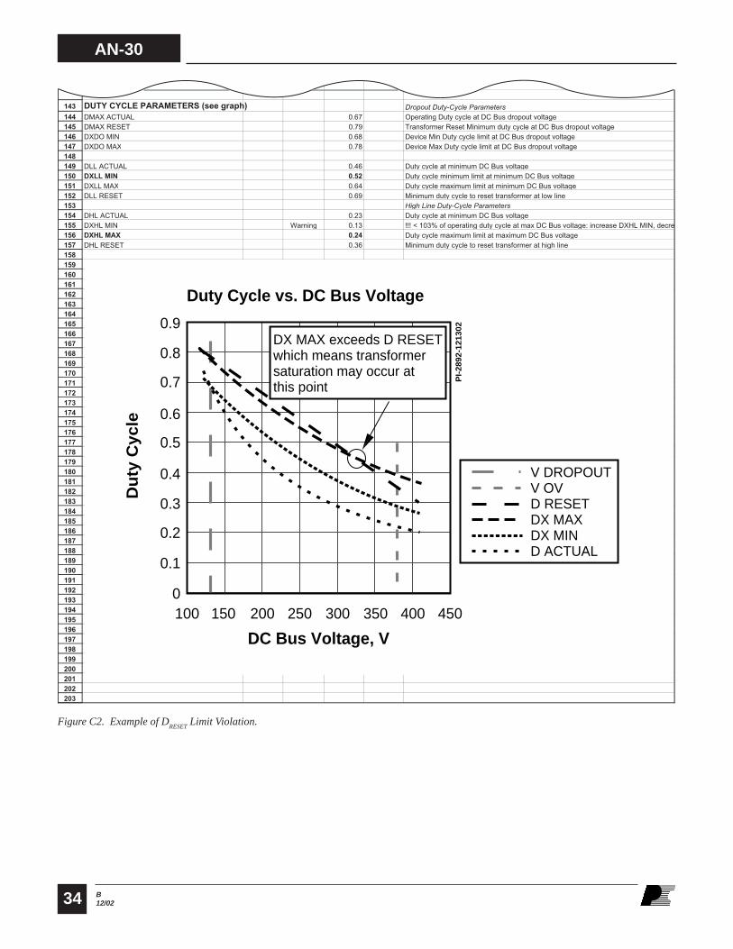
AN-30
34 B12/02
143
144
145
146
147
148
149
150
151
152
153
154
155
156
157
158
159
160
161
162
163
164
165
166
167
168
169
170
171
172
173
174
175
176
177
178
179
180
181
182
183
184
185
186
187
188
189
190
191
192
193
194
195
196
197
198
199
200
201
202
203
DUTY CYCLE PARAMETERS (see graph) Dropout Duty-Cycle Parameters
DMAX ACTUAL 0.67 Operating Duty cycle at DC Bus dropout voltage
DMAX RESET 0.79 Transformer Reset Minimum duty cycle at DC Bus dropout voltage
DXDO MIN 0.68 Device Min Duty cycle limit at DC Bus dropout voltage
DXDO MAX 0.78 Device Max Duty cycle limit at DC Bus dropout voltage
DLL ACTUAL 0.46 Duty cycle at minimum DC Bus voltage
DXLL MIN 0.52 Duty cycle minimum limit at minimum DC Bus voltage
DXLL MAX 0.64 Duty cycle maximum limit at minimum DC Bus voltage
DLL RESET 0.69 Minimum duty cycle to reset transformer at low line
High Line Duty-Cycle Parameters
DHL ACTUAL 0.23 Duty cycle at minimum DC Bus voltage
DXHL MIN Warning 0.13 !!! < 103% of operating duty cycle at max DC Bus voltage: increase DXHL MIN, decre
DXHL MAX 0.24 Duty cycle maximum limit at maximum DC Bus voltage
DHL RESET 0.36 Minimum duty cycle to reset transformer at high line
0.0
0.1
0.2
0.3
0.4
0.5
0.6
0.7
0.8
0.9
100 150 200 250 300 350 400 450
DC Bus Voltage, V
D_ACTUAL D_RESET DX_MIN DX_MAX V_OV V_DROPOUT
Duty Cycle vs DC Bus Voltage
0.9
0.6
0.5
0.8
0.7
100 150 200 250 300 350 400 450
DC Bus Voltage, V
Duty Cycle vs. DC Bus Voltage
Du
ty C
ycle
PI-
2892
-121
302
0
0.3
0.2
0.1
0.4
DX MAX exceeds D RESETwhich means transformersaturation may occur at this point
V DROPOUTV OVD RESETDX MAXDX MIND ACTUAL
Figure C2. Example of DRESET
Limit Violation.

AN-30
35B12/02
Figure C3. Example of DACTUAL
(Regulation) Limit Violation.
143
144
145
146
147
148
149
150
151
152
153
154
155
156
157
158
159
160
161
162
163
164
165
166
167
168
169
170
171
172
173
174
175
176
177
178
179
180
181
182
183
184
185
186
187
188
189
190
191
192
193
194
195
196
197
198
199
200
201
202
203
DUTY CYCLE PARAMETERS (see graph) Dropout Duty-Cycle Parameters
DMAX ACTUAL 0.67 Operating Duty cycle at DC Bus dropout voltage
DMAX RESET 0.79 Transformer Reset Minimum duty cycle at DC Bus dropout voltage
DXDO MIN 0.69 Device Min Duty cycle limit at DC Bus dropout voltage
DXDO MAX 0.78 Device Max Duty cycle limit at DC Bus dropout voltage
DLL ACTUAL 0.46 Duty cycle at minimum DC Bus voltage
DXLL MIN 0.56 Duty cycle minimum limit at minimum DC Bus voltage
DXLL MAX 0.66 Duty cycle maximum limit at minimum DC Bus voltage
DLL RESET 0.69 Minimum duty cycle to reset transformer at low line
High Line Duty-Cycle Parameters
DHL ACTUAL 0.23 Duty cycle at minimum DC Bus voltage
DXHL MIN 0.30 Duty cycle minimum limit at maximum DC Bus voltage
DXHL MAX Warning 0.39 !!! > reset duty cycle at VMAX : decrease DXHL MAX, increase VDSOP
DHL RESET 0.36 Minimum duty cycle to reset transformer at high line
0.0
0.1
0.2
0.3
0.4
0.5
0.6
0.7
0.8
0.9
100 150 200 250 300 350 400 450
DC Bus Voltage, V
D_ACTUAL D_RESET DX_MIN DX_MAX V_OV V_DROPOUT
Duty Cycle vs DC Bus Voltage
0.9
0.6
0.5
0.8
0.7
100 150 200 250 300 350 400 450
DC Bus Voltage, V
Duty Cycle vs. DC Bus Voltage
Du
ty C
ycle
PI-
2891
-121
302
0
0.3
0.2
0.1
0.4
D ACTUAL exceeds DX MIN curve - hence low tolerance device will cause supply todrop out of regulation
V DROPOUTV OVD RESETDX MAXDX MIND ACTUAL

AN-30
36 B12/02
Selection of RC
The value of RC
is calculated by the spreadsheet. In EP-12 this value is calculated as:R
C = 40.26 kΩ (RC, F139)
Choose closest standard available value, RC
= 43.2 kΩ, 0.125 W
Selection of RD
The value of RD is automatically calculated by the spreadsheet. In EP-12 this value is calculated as:
RD = 126.70 kΩ (RD, F143)
Choose closest standard available value, RD = 130 kΩ, 0.125 W
Selection of Capacitor CVS
The capacitor CVS
is also estimated by the spreadsheet. For EP-12, the value from the equation is approximately 93 pF.
If the calculated value is unavailable choose next higher standard available value.Choose C
VS = 100 pF, 100 V (CVS, F141)

AN-30
37B12/02
Spreadsheet
A B D F G I
1
2
3
4
5
6
7
8
9
10
11
12
13
14
15
16
17
18
19
20
21
22
23
24
25
26
27
28
29
30
31
32
33
34
35
36
37
38
39
40
41
42
43
44
45
46
47
48
49
50
51
52
53
54
55
56
57
58
59
60
61
62
63
64
65
66
67
68
69
70
71
72
73
74
75
76
77
ACDC_TOPGXForward_Rev_1.03_061802
Copyright Power Integrations Inc. 2002
INPUT INFO OUTPUT UNIT
ACDC_TOPGXFwd_061802_r103.xls: TOPSwitch-GX Forward Transformer
Design Spreadsheet
OUTPUT VOLTAGE AND CURRENTEP12 PC Main power supply
VMAIN 5 Volts Main output voltage
IMAIN 12 Amps Main output current
VMAINMA 3.3 Volts Magamp output voltage
IMAINMA 12 Amps Magamp output current
VAUX1 12 Volts Auxiliary output voltage
IAUX1 4 Amps Auxiliary output current
VIND1 Volts Independant output voltage
IND1 Amps Independent output current
PO 147.6 Watts Total output power
ENTER APPLICATION VARIABLES
VACMIN 90 AC volts Minimum AC input voltage. Input voltage doubler circuit is assumed.
VACMAX 132 AC volts Maximum AC input voltage. Input voltage doubler circuit is assumed.
VMIN 188 Volts Minimum DC Bus voltage at low line input
VMAX 373 Volts Maximum DC Bus voltage at high line input
CIN 165 uFarads Equivalent bulk input capacitance. Input voltage doubler circuit is assumed.
fL 50 Hz Input AC line frequency
tc 3.0 mSeconds Estimate input bridge diode conduction time
th 16.0 mSeconds Minimum required hold-up time from VDROPOUT to VHOLDUP
EFF 0.75 Efficiency estimate to determine minimum DC Bus voltage
VHOLDUP 188 Volts DC Bus voltage at start of hold-up time (default VMIN)
VDROPOUT 132 132 Volts DC Bus Voltage at end of hold-up time
DMAX GOAL 0.7 0.70 Maximum duty cycle at DC dropout voltage
VDSOP 580 Volts Maximum operating drain voltage
KDI 0.15 Maximum output current ripple factor at maximum DC Bus voltage
REF AUX1 1 DC Stack Enter one ('1') for DC stacked , zero ('0') Independent winding
ENTER TOPSWITCH VARIABLES
TOPSwitch top247 Universal Doubled 115V/230V
Chosen Device TOP247 Power Out - 165W
ILIMIT 3.348 3.852 Amps From TOPSwitch-GX datasheet
fS 124000 132000 Hertz From TOPSwitch-GX+H76 datasheet
KI 0.81 Ilimit reduction (KI=1.0 for default ILIMIT, KI <1.0 for lower ILIMIT)
RX 7.78 kOhm Maximum current limit resistance to ensure KI >= 0.81 setting
ILIMITEXT 2.712 Amps External current limit
VDS 8.1 Volts TOPSwitch-GX average on-state Drain to Source Voltage
DIODE Vf SELECTION
VDMAIN 0.5 Volts Main output rectifiers forward voltage drop (Schottky)
VDMAINMA 0.5 Volts Magamp output rectifiers forward voltage drop (Schottky)
VDAUX1 0.7 Volts Auxiliary output rectifiers forward voltage drop (Ultrafast)
VDIND1 0 Volts Independent output rectifiers forward voltage drop (Schottky)
VDB 0.7 Volts Bias output rectifier conduction drop
BRIDGE RECTIFIER DIODE SELECTION
VPIVAC 467 Volts Maximum voltage across Bridge rectifier diode
IDAVBR 0.773 Amps Average Bridge Rectifier Current
TRANSFORMER CORE SELECTION
Core Type eer28l
Core EER28L P/N: PC40EER28L-Z
Bobbin EER28L_BO P/N: BEER-28L-1112CPH
AE 0.814 cm^2 Core Effective Cross Sectional Area
LE 7.55 cm Core Effective Path Length
AL 2520 nH/T^2 Ungapped Core Effective Inductance
BW 21.8 mm Bobbin Physical Winding Width
LG MAX 0.02 mm Maximum actual gap when zero gap specified
R FACTOR 9% 9% % Percentage of total PS losses lost in transformer windings; default 10%
M 3.0 mm Transformer margin
L 0.80 Transformer primary layers
NMAIN 3 Main rounded turns
TRANSFORMER DESIGN PARAMETERS
NP 45 45 Primary rounded turns
NB 6 Bias turns to maintain 8V minimum input voltage, light load
NAUX1 4 Auxiliary rounded turns (DC stacked on Main winding)
VAUX1 ACTUAL 11.63 Volts Approx. Aux output voltage with NAUX1 = 4 Turns and DC stack
NIND1 0 Independent rounded turns (separate winding)
VIND1 ACTUAL 0.00 Volts Approximate Independent output voltage with NIND1 = 0 turns
BM 1816 Gauss Maximum operating flux density at minimum switching frequency
BP 2884 Gauss Maximum peak flux density at minimum switching frequency
LP MIN 3.419 mHenries Minimum primary magnetizing inductance (assumes LGMAX=20um)
IMAG 0.189 Amps Peak magnetizing current at minimum input voltage

AN-30
38 B12/02
A B D F G I
78
79
80
81
82
83
84
85
86
87
88
89
90
91
92
93
94
95
96
97
98
99
100
101
102
103
104
105
106
107
108
109
110
111
112
113
114
115
116
117
118
119
120
121
122
123
124
125
126
127
128
129
130
131
132
133
134
135
136
137
138
139
140
141
142
143
144
145
146
147
148
149
150
151
152
153
154
155
156
157
OD_P 0.33 mm Primary wire outer diameter
AWG_P 28 AWG Primary Wire Gauge (rounded to maximum AWG value)
CURRENT WAVESHAPE PARAMETERS
IP 2.451 Amps Maximum peak primary current at maximum DC Bus voltage
IPRMS 1.460 Amps Maximum primary RMS current at minimum DC Bus voltage
INDUCTOR OUTPUT PARAMETERS
LMAIN 10.0 uHenries Main / Auxiliary coupled output inductance (referred to Main winding)
WLMAIN 2286 uJoules Main / Auxiliary coupled output inductor full-load stored energy
KDIMAIN 0.150 Current ripple factor of combined Main and Aux1 outputs
LMAINMA 12.3 uHenries Magamp output inductance
WLMAINMA 888 uJoules Magamp output inductor full-load stored energy
KDIMAINMA 0.150 Current ripple factor for Magamp output
LIND1 0.0 uHenries Independent output inductance
WLIND1 0.0 uJoules Independent output inductor full-load stored energy
KDIIND1 0.000 Current ripple factor for Independent output
SECONDARY OUTPUT PARAMETERS
ISMAINRMSLL 15.61 Amps Maximum transformer secondary RMS current (DC Stack)
ISAUX1RMSLL 2.42 Amps Maximum transformer secondary RMS current (DC Stack)
ISIND1RMSDLL 0.00 Amps Maximum transformer secondary RMS current
IDAVMAIN 12.3 Amps Maximum average current, Main rectifier (single device rating)
IDAVMAINMA 9.3 Amps Maximum average current, Magamp rectifier (single device rating)
IDAVAUX1 3.1 Amps Maximum average current, Auxiliary rectifier (single device rating)
IDAVIND1 0.0 Amps Maximum average current, Independent rectifier (single device rating)
IRMSMAIN 0.52 Amps Maximum RMS current, Main output capacitor
IRMSMAINMA 0.52 Amps Maximum RMS current, Magamp output capacitor
IRMSAUX1 0.17 Amps Maximum RMS current, Auxiliary output capacitor
IRMSIND1 0.00 Amps Maximum RMS current, Independent output capacitor
DIODE PIV No derating
VPIVMAIN 29.5 Volts Main output rectifiers peak-inverse voltage
VPIVMAINMA 29.5 Volts Magamp output rectifiers peak-inverse voltage
VPIVAUX1 34.9 Volts Auxiliary output rectifiers peak-inverse voltage
VPIVIND1 0.0 Volts Independent output rectifiers peak-inverse voltage
VPIVB 102.1 Volts Bias output rectifier peak-inverse voltage
Optocoupler
VCEO OPTO 49.8 Volts Maximum optocoupler collector-emitter voltage
UNDER-VOLTAGE LOCKOUT CIRCUIT PARAMETERS
VACUVL 68 AC volts AC undervoltage lockout voltage; On-Off transition
VACUV 78 AC volts AC undervoltage lockout voltage; Off-On transition
VACUVX 68
RUVA 2.23 MOhm Resistor RUVA value
RUVB 523.73 kOhm Resistor RUVB value
RUVC 75.91 kOhm Resistor RUVC value
VACUVL ACTUAL 67.50 AC volts Actual AC undervoltage lockout voltage; On-Off transition
VACUVX ACTUAL 70.36 AC volts Actual AC undervoltage lockout voltage; Off-On transition
DUTY CYCLE LIMIT CIRCUIT PARAMETERS
VZ 6.80 Volts Zener voltage used within DLIM circuit
VOV 380 Volts Approximate frequency reduction voltage (determines CVS value)
RA 2.20 MOhm Resistor RA value
RB 2.20 MOhm Resistor RB value
RC 40.26 kOhm Resistor RC value
RD 126.70 kOhm Resistor RD value
CVS 92.98 pF Capacitor CVS value
DUTY CYCLE PARAMETERS (see graph) Dropout Duty-Cycle Parameters
DMAX ACTUAL 0.69 Operating Duty cycle at DC Bus dropout voltage
DMAX RESET 0.79 Transformer Reset Minimum duty cycle at DC Bus dropout voltage
DXDO MIN 0.70 Device Min Duty cycle limit at DC Bus dropout voltage
DXDO MAX Caution 0.79 !!! >DMAXRESET from VMIN to VDROPOUT. NOT hazardous
DLL ACTUAL 0.47 Duty cycle at minimum DC Bus voltage
DXLL MIN 0.55 Duty cycle minimum limit at minimum DC Bus voltage
DXLL MAX 0.67 Duty cycle maximum limit at minimum DC Bus voltage
DLL RESET 0.69 Minimum duty cycle to reset transformer at low line
High Line Duty-Cycle Parameters
DHL ACTUAL 0.23 Duty cycle at minimum DC Bus voltage
DXHL MIN 0.24 Duty cycle minimum limit at maximum DC Bus voltage
DXHL MAX 0.35 Duty cycle maximum limit at maximum DC Bus voltage
DHL RESET 0.36 Minimum duty cycle to reset transformer at high line

AN-30
39B12/02
A B D F G I
158
159
160
161
162
163
164
165
166
167
168
169
170
171
172
173
174
175
176
177
178
179
180
181
182
183
184
185
186
187
188
189
190
191
192
193
194
195
196
197
198
199
200
201
202
203
0.0
0.1
0.2
0.3
0.4
0.5
0.6
0.7
0.8
0.9
100 150 200 250 300 350 400 450
DC Bus Voltage, V
D_ACTUAL D_RESET DX_MIN DX_MAX V_OV V_DROPOUT
Duty Cycle vs DC Bus Voltage
0.9
0.6
0.5
0.8
0.7
100 150 200 250 300 350 400 450
DC Bus Voltage, V
Duty Cycle vs. DC Bus VoltageD
uty
Cyc
le
PI-
2890
-121
302
0
0.3
0.2
0.1
0.4 V DROPOUTV OVD RESETDX MAXDX MIND ACTUAL

AN-30
40 B12/02
SINGAPOREPower Integrations, Singapore51 Goldhill Plaza #16-05Republic of Singapore 308900Phone: +65-6358-2160Fax: +65-6358-2015e-mail: [email protected]
WORLD HEADQUARTERSAMERICASPower Integrations, Inc.5245 Hellyer AvenueSan Jose, CA 95138 USAMain: +1 408-414-9200Customer Service:Phone: +1 408-414-9665Fax: +1 408-414-9765e-mail: [email protected]
For the latest updates, visit our Web site: www.powerint.comPower Integrations reserves the right to make changes to its products at any time to improve reliability or manufacturability.Power Integrations does not assume any liability arising from the use of any device or circuit described herein, nor does it conveyany license under its patent rights or the rights of others.
The products and applications illustrated herein (including circuits external to the products and transformer construction) may becovered by one or more U.S. and foreign patents or potentially by pending U.S. and foreign patent applications assigned to PowerIntegrations. A complete list of Power Integrations’ patents may be found at www.powerint.com.
The PI Logo, TOPSwitch, TinySwitch, LinkSwitch and EcoSmart are registered trademarks of Power Integrations, Inc.PI Expert is a trademark of Power Integrations, Inc. ©Copyright 2002, Power Integrations, Inc.
TAIWANPower IntegrationsInternational Holdings, Inc.17F-3, No. 510Chung Hsiao E. Rdl,Sec. 5,Taipei, Taiwan 110, R.O.C.Phone: +886-2-2727-1221Fax: +886-2-2727-1223e-mail: [email protected]
CHINAPower IntegrationsInternational Holdings, Inc.Rm# 1705, Bao Hua Bldg.1016 Hua Qiang Bei LuShenzhen Guangdong, 518031ChinaPhone: +86-755-8367-5143Fax: +86-755-8377-9610e-mail: [email protected]
EUROPE & AFRICAPower Integrations (Europe) Ltd.Centennial CourtEasthampstead RoadBracknellBerkshire, RG12 1YQUnited KingdomPhone: +44-1344-462-300Fax: +44-1344-311-732e-mail: [email protected]
KOREAPower IntegrationsInternational Holdings, Inc.Rm# 402, Handuk Building649-4 Yeoksam-Dong, Kangnam-Gu,Seoul, KoreaPhone: +82-2-782-2840Fax: +82-2-782-4427e-mail: [email protected]
JAPANPower Integrations, K.K.Keihin-Tatemono 1st Bldg.12-20 Shin-Yokohama 2-ChomeKohoku-ku, Yokohama-shi,Kanagawa 222-0033, JapanPhone: +81-45-471-1021Fax: +81-45-471-3717e-mail: [email protected]
INDIA (Technical Support)Innovatech#1, 8th Main RoadVasanthnagarBangalore, India 560052Phone: +91-80-226-6023Fax: +91-80-228-9727e-mail: [email protected]
APPLICATIONS HOTLINE APPLICATIONS FAXWorld Wide +1-408-414-9660 World Wide +1-408-414-9760