Embed Size (px)
Citation preview

Design, Fabrication and Measurement ofIntegrated Bragg Grating Optical Filters
by
Thomas E. Murphy
B.S. Electrical Engineering, Rice University (1994)B.A. Physics, Rice University (1994)
S.M. Electrical Engineering, Massachusetts Institute of Technology (1997)
Submitted to the Department of Electrical Engineering and ComputerScience in partial fulfillment of the requirements for the degree of
Doctor of Philosophy
at the
MASSACHUSETTS INSTITUTE OF TECHNOLOGY
February, 2001
c© Massachusetts Institute of Technology, 2001. All rights reserved
Author . . . . . . . . . . . . . . . . . . . . . . . . . . . . . . . . . . . . . . . . . . . . . . . . . . . . . . . . . . . . . . . . . . . . . . . . . . . . . . . . . .Department of Electrical Engineering and Computer Science
November 6, 2000
Certified by. . . . . . . . . . . . . . . . . . . . . . . . . . . . . . . . . . . . . . . . . . . . . . . . . . . . . . . . . . . . . . . . . . . . . . . . . . . . . .Henry I. Smith
Keithly Professor of Electrical EngineeringThesis Supervisor
Accepted by . . . . . . . . . . . . . . . . . . . . . . . . . . . . . . . . . . . . . . . . . . . . . . . . . . . . . . . . . . . . . . . . . . . . . . . . . . . . .Arthur C. Smith
Chairman, Deparment Committee on Graduate Students


Design, Fabrication and Measurement ofIntegrated Bragg Grating Optical Filters
by
Thomas E. Murphy
Submitted to the Department of Electrical Engineering and Computer Science onNovember 6, 2000, in partial fulfillment of the requirements for the degree of
Doctor of Philosophy
Abstract
The subject of this thesis is the design, analysis, fabrication, and characterization of in-tegrated Bragg grating optical filters. We begin by describing the design and analysis ofthree essential building blocks needed for integrated Bragg grating filters: waveguides,directional couplers and Bragg gratings. Next, we describe and implement a flexible fabri-cation methodology for building integrated Bragg gratings filters in two important mate-rial systems: doped-glass channel waveguides and silicon-on-insulator ridge waveguides.Finally, we evaluate the performance of the fabricated directional couplers and Bragg grat-ings, comparing experimental results with theoretical predictions.
Thesis Supervisor: Henry I. SmithTitle: Keithly Professor of Electrical Engineering

Acknowledgments
First and foremost, I would like to thank Prof. Hank Smith who supported and advisedme throughout my time MIT. The goal of a Ph.D. program is not only to accomplish spe-cific research goals but also to train one as a scientist. More than anyone else, Hank hascontributed to this second goal. He has given me a tremendous amount of freedom toset my own goals and seek my own solutions to problems, but at the same time he hasalways been approachable and encouraging when I got stuck. Perhaps one of the mostvaluable skills I have acquired (hopefully) under Hank’s tutelage is the ability to writeclearly and present my work effectively. To the extent that the reader finds this work clearand understandable, I am deeply indebted to Hank.
For many professors, the role of academic adviser unfortunately entails little morethan signing forms and reminding graduate students of upcoming deadlines. I have beenextremely fortunate to have an academic adviser who has done much more than this.Terry Orlando has been a great source of guidance and advice, both professional and per-sonal. He has gone out of his way to make himself available outside of the usual biannualregistration-day meetings. I would like to thank Terry for always taking the time to listento me, for giving me honest and unbiased advice, and for encouraging me at a time whenI really needed encouragement.
In the spring of 1999, I had the unique opportunity to work as a teaching assistant withProf. Greg Wornell. This semester proved to be one of the most rewarding and stimulatingduring my time as a graduate student. I’m grateful to Greg for giving me ample teachingresponsibilities that I wouldn’t have found in other courses.
I have benefited from many stimulating conversations with Prof. Hermann Haus, andI have great esteem for his unrivaled enthusiasm and physical insight. I would also liketo acknowledge Dr. Brent Little, who provided the original underlying theory for mywork on insensitive couplers. Brent has also been a valuable source of practical knowledgeon optical physics and electromagnetics. I’m grateful to Prof. Erich Ippen, Prof. LionelKimerling, and Anu Agarwal who agreed to serve on my thesis committee.
MIT has been a wonderful place to conduct research, mostly because of the talentedstudents who have worked alongside me. I am especially indebted to the members ofthe optics subgroup, who directly contributed to this work. Jay Damask was one of myfirst mentors at MIT, and the person who first introduced me to the world integrated op-tics. Much of my intuition and a great deal of my research style can be traced back toJay. I couldn’t possibly enumerate the ways in which Mike Lim has helped me out in thelab; many of the lithographic feats presented in this work could not have been accom-plished without Mike’s helpful advice and assistance. Juan Ferrera was for years the resi-dent electron beam lithography expert in our lab, and he is responsible for developing thetechnique of adding alignment marks to interference-lithography-generated x-ray masks.He also provided invaluable help with the interference lithography system. Additionally,Juan taught me much of what I know about UNIX network administration. I’m gratefulto Vince Wong, who was very generous with his time even when he was extremely busy.

Todd Hastings has been exceptionally helpful with electron-beam lithography and metrol-ogy. When I have new ideas, Todd is usually one of the first people I run them by. JalalKhan has been a great officemate, and a valuable source of advice on optics modeling.Oliver Stolz worked very diligently with me for several months to investigate birefrin-gence in silicon waveguides. I truly enjoyed working with him on this project, and myown research has benefited directly from his careful measurements and calculations.
Outside of the optics team, I would like to thank the other students and staff of theNanoStructures Lab. Maya Farhoud has been a wonderful officemate, and more impor-tantly a great friend. The past five years would not have been nearly as much fun withouther companionship. Mark Mondol performed much of the electron-beam lithography forme, and more generally he has also been an outstanding advocate for the students in ourgroup. I have truly enjoyed working with Mark, and I will miss his sense of humor andhis exceptional patience. Jim Daley deserves almost all the credit for keeping the lab upand running. Jim Carter has been a very valuable source of technical assistance in almostall areas of laboratory work. I would like to thank Mike Walsh, who developed the Lloyd’smirror lithography system, and spent the time to teach me how to use it. Mike has alsocontributed very valuable software which I used to model the reflection from multilayerstacks. Minghao Qi has greatly assisted me with the tasks of network administration, andDario Gil has helped me out by taking over the job of maintaining our website. I wouldalso like to thank Tim Savas, Keith Jackson, James Goodberlet, and Dave Carter for theirhelpful advice. I have also enjoyed many stimulating conversations about electromagneticsimulation with Rajesh Menon. Mark Schattenburg has been a tremendous source of ad-vice on topics ranging from interference lithography to x-ray absorption. Cindy Lewis alsodeserves recognition for handling all of the administrative tasks of the group.
Several individuals outside of my research group have also helped to make my job atMIT easier. Desmond Lim deserves credit for teaching me the art of polishing waveguidefacets. I’ve enjoyed sharing both lab space and ideas with J. P. Laine. Dave Foss, the localcomputer and networking guru, has been a tremendously helpful resource when we’vehad computer failures. Peggy Carney helped to straighten out my stipend on numerousoccasions during my first three years as a fellowship student. Marilyn Pierce has helpedwith everything from selecting an oral exam comittee to registering for courses. I’d like tothank the folks over at the ATIC lab for all of their useful advice on more effectively usingspeech recognition software. I’m grateful to Alice White and Ed Laskowski at Bell Labs forall of the technical advice they’ve give me on waveguide technology, and for the dozens ofglass waveguide substrates that they generously provided for this work.
Erik Thoen shared an apartment with me for five of my years at MIT, and he’s beenone of my most trusted friends. I’m grateful to Erik for helping me to always see thelighter side of life. Ii-Lun Chen has patiently stood by my side through some of the mostdifficult and strenuous times of my Ph.D. work. She has been a deep source of warmthand inspiration in my life, and a constant source of moral support.
I would like to thank the National Science Foundation for supporting me during myfirst three years as a graduate student, and DARPA for supporting my work as a researchassistant in the latter years. I’m grateful to the MIT-Lemelson foundation and Unisphere

Corp., for recognizing and supporting our accomplishments.
Finally, I would like to acknowledge my family for their tireless love and support overthe years. A special word of thanks goes to my aunt Roseanne Cook: having made itthrough her own Ph.D. program, her words of encouragement were especially under-standing and empathetic. I would like to thank my parents, John and Josephine Murphy,for working hard to provide me with the best educational opportunities, for supporting allof my decisions, and for serving as the shining examples of how to live a rewarding andmeaningful life.

Contents
1 Introduction 11
2 Theory and Analysis 172.1 Modal Analysis of Waveguides . . . . . . . . . . . . . . . . . . . . . . . . . . 18
2.1.1 Eigenmode Equations for Dielectric Waveguides . . . . . . . . . . . . 182.1.2 Normalization and Orthogonality . . . . . . . . . . . . . . . . . . . . 232.1.3 Weakly-Guiding Waveguides . . . . . . . . . . . . . . . . . . . . . . . 242.1.4 Finite Difference Methods . . . . . . . . . . . . . . . . . . . . . . . . . 252.1.5 Computed Eigenmodes for Optical Waveguides . . . . . . . . . . . . 33
2.2 Coupled Waveguides . . . . . . . . . . . . . . . . . . . . . . . . . . . . . . . . 332.2.1 Variational Approach . . . . . . . . . . . . . . . . . . . . . . . . . . . 372.2.2 Exact Modal Analysis . . . . . . . . . . . . . . . . . . . . . . . . . . . 432.2.3 Real Waveguide Couplers . . . . . . . . . . . . . . . . . . . . . . . . . 462.2.4 Results of Coupled Mode Analysis . . . . . . . . . . . . . . . . . . . . 492.2.5 Design of Insensitive Couplers . . . . . . . . . . . . . . . . . . . . . . 50
2.3 Bragg Gratings . . . . . . . . . . . . . . . . . . . . . . . . . . . . . . . . . . . 582.3.1 Bragg Grating Basics . . . . . . . . . . . . . . . . . . . . . . . . . . . . 592.3.2 Contradirectional Coupled Mode Theory . . . . . . . . . . . . . . . . 612.3.3 Spectral Response of Bragg Grating . . . . . . . . . . . . . . . . . . . 672.3.4 Calculation of Grating Strength . . . . . . . . . . . . . . . . . . . . . . 722.3.5 Apodized and Chirped Bragg Gratings . . . . . . . . . . . . . . . . . 78
2.4 Transfer Matrix Methods . . . . . . . . . . . . . . . . . . . . . . . . . . . . . . 842.4.1 Multi-Waveguide Systems . . . . . . . . . . . . . . . . . . . . . . . . . 842.4.2 Transfer Matrices and Scattering Matrices . . . . . . . . . . . . . . . . 862.4.3 Useful Transfer Matrices . . . . . . . . . . . . . . . . . . . . . . . . . . 882.4.4 The Integrated Interferometer . . . . . . . . . . . . . . . . . . . . . . . 91
2.5 Summary . . . . . . . . . . . . . . . . . . . . . . . . . . . . . . . . . . . . . . . 99
3 Fabrication 101
7

8 CONTENTS
3.1 Fabrication of Waveguides and Couplers . . . . . . . . . . . . . . . . . . . . 1023.1.1 Integrated Waveguide Technology . . . . . . . . . . . . . . . . . . . . 1023.1.2 Pattern Generation and Waveguide CAD . . . . . . . . . . . . . . . . 1083.1.3 Glass Channel Waveguides and Couplers . . . . . . . . . . . . . . . . 1113.1.4 SOI Waveguides . . . . . . . . . . . . . . . . . . . . . . . . . . . . . . 114
3.2 Lithographic Techniques for Bragg Gratings . . . . . . . . . . . . . . . . . . . 1203.2.1 Interference Lithography . . . . . . . . . . . . . . . . . . . . . . . . . 1203.2.2 X-ray Lithography . . . . . . . . . . . . . . . . . . . . . . . . . . . . . 1253.2.3 Electron-Beam Lithography . . . . . . . . . . . . . . . . . . . . . . . . 1293.2.4 Phase Mask Interference Lithography . . . . . . . . . . . . . . . . . . 1303.2.5 Other Techniques for Producing Bragg Gratings . . . . . . . . . . . . 131
3.3 Multilevel Lithography: Waveguides with Gratings . . . . . . . . . . . . . . 1333.3.1 Challenges to Building Integrated Bragg Gratings . . . . . . . . . . . 1333.3.2 Prior Work on Integrated Bragg Gratings . . . . . . . . . . . . . . . . 1363.3.3 Bragg Gratings on Glass Waveguides . . . . . . . . . . . . . . . . . . 1373.3.4 Bragg Gratings on Silicon Waveguides . . . . . . . . . . . . . . . . . . 151
3.4 Summary . . . . . . . . . . . . . . . . . . . . . . . . . . . . . . . . . . . . . . . 162
4 Measurement 163
4.1 Glass Waveguide Measurements . . . . . . . . . . . . . . . . . . . . . . . . . 1634.1.1 Summary of Device Design . . . . . . . . . . . . . . . . . . . . . . . . 1634.1.2 Measurement Technique . . . . . . . . . . . . . . . . . . . . . . . . . . 1654.1.3 Measurement Results . . . . . . . . . . . . . . . . . . . . . . . . . . . 169
4.2 Silicon-on-Insulator Waveguide Measurements . . . . . . . . . . . . . . . . . 1764.2.1 Loss Characterization . . . . . . . . . . . . . . . . . . . . . . . . . . . 1764.2.2 Measurement of Integrated Bragg Gratings . . . . . . . . . . . . . . . 181
4.3 Summary . . . . . . . . . . . . . . . . . . . . . . . . . . . . . . . . . . . . . . . 189
5 Conclusions 1935.1 Summary . . . . . . . . . . . . . . . . . . . . . . . . . . . . . . . . . . . . . . . 1935.2 Future Work . . . . . . . . . . . . . . . . . . . . . . . . . . . . . . . . . . . . . 194
A Finite Difference Modesolver 197A.1 Vector Finite Difference Method . . . . . . . . . . . . . . . . . . . . . . . . . . 197A.2 Finite Difference Boundary Conditions . . . . . . . . . . . . . . . . . . . . . . 202A.3 Finite Difference Equations for Transverse H Fields . . . . . . . . . . . . . . 206A.4 Semivectorial Finite Difference Method . . . . . . . . . . . . . . . . . . . . . 207
B Waveguide Pattern Generation Software 217

CONTENTS 9
C Phase Distortion in Bragg Gratings 221C.1 Evidence of Chirp in Bragg Gratings . . . . . . . . . . . . . . . . . . . . . . . 221C.2 Sources of Distortion . . . . . . . . . . . . . . . . . . . . . . . . . . . . . . . . 226C.3 Measurements of Distortion . . . . . . . . . . . . . . . . . . . . . . . . . . . . 231C.4 Summary . . . . . . . . . . . . . . . . . . . . . . . . . . . . . . . . . . . . . . . 234
References 236

10 CONTENTS

Chapter 1
Introduction
During the past decade, the world has seen an explosive growth in optical telecommuni-cations, fueled in part by the rapid expansion of the Internet. Not only are optical telecom-munications systems constantly improving in their performance and capacity [1, 2], butthe deployment of optical systems is spreading deeper into the consumer market. Tenyears ago, optical systems were primarily used in point-to-point long distance links [3, 4].In the future, fiber-optic networks will be routed directly into neighborhoods, households,and even to the back of each computer [5, 6]. In the more distant future, it is possible thateven the signals bouncing between the different components inside the computer will betransmitted and received optically [7]. As optical fiber gradually replaces copper cables, itwill become necessary for many of the electronic network components to be replaced byequivalent optical components: splitters, filters, routers, and switches.
In order for these optical components to be compact, manufacturable, low-cost, andintegratable, it is highly desirable that they be fabricated on a planar surface. The in-tegrated circuit revolution of the 1960s (which continues today) clearly demonstrated thetremendous potential afforded by planar lithographic techniques. Bragg gratings offer onepossible solution for constructing integrated optical filters [8].
This thesis concerns the design, construction, and measurement of integrated opticalfilters based on Bragg gratings. The general objective of this thesis is to better understandhow Bragg gratings work, to develop a flexible fabrication scheme for building Bragg grat-ings filters, and to evaluate the performance of fabricated devices.
Figure 1.1a depicts the structure of an integrated Bragg grating filter. A fine-periodcorrugation etched into the surface of an otherwise uniform waveguide creates a coupling
11

12 CHAPTER 1. INTRODUCTION
between the forward- and backward-traveling light in the structure. The Bragg grating isanalogous to the dielectric stack mirror depicted in Fig. 1.1b. The grating reflects light in anarrow wavelength range, centered at the so-called Bragg wavelength. As such, the Bragggrating forms a convenient implementation of an integrated optical bandpass filter.
Fiber Bragg gratings are widely used in optical telecommunications systems, for appli-cations ranging from dispersion compensation to add/drop filtering. The integrated Bragggratings considered here offer several advantages over their fiber counterparts. First, theintegrated Bragg gratings described in this work are formed by physically corrugating awaveguide, and therefore they do not rely upon a photorefractive index change. This al-lows us to build Bragg gratings in materials which are not photorefractive (e.g. Si or InP),and it potentially allows stronger gratings to be constructed since the grating strength isnot limited by the photorefractive effect. Second, the integrated Bragg gratings can bemade smaller, and packed closer together than fiber-optic devices. Third, the planar fabri-cation process gives better control over the device dimensions. For example, the beginningand end of the Bragg grating can be sharply delineated rather than continuously tapered,abrupt phase shifts can be introduced at any point in the grating, and precise period controlcan be achieved – the integrated Bragg grating can be engineered on a tooth-by-tooth ba-sis. Finally, multiple levels of lithography can be combined, with precise nano-alignmentbetween them, allowing the Bragg gratings to be integrated with couplers, splitters, andother electronic or photonic components.
Figure 1.2 illustrates schematically the hierarchy of integrated optical devices whichwill be discussed in this thesis, beginning with the simplest structure: the integrated wave-guide.
Figure 1.2b depicts a slightly more complicated device: the integrated directional cou-pler, which is designed to transfer power from one waveguide to another. Figure 1.2cdepicts a more advanced version of the integrated directional coupler, which provideswavelength-, and polarization-insensitive performance.
Figure 1.2d depicts the simplest form of an integrated Bragg grating filter. In this struc-ture, the filtered signal is reflected back into the input port of the device. Figure 1.2e depictsa more sophisticated Bragg grating filter, in which the grating is apodized, or windowed inorder to provide a more optimal spectral response. One drawback of this topology is thatfurther processing is required to separate the reflected filtered signal from the input signal.This can be accomplished using an optical circulator [9], but the circulator is an expensivedevice which cannot be easily integrated.

13
...
n1
n2
n1
n2
n1
n2
n1
n2
n1
Λ
R T
R TΛ
Integrated Waveguide
(a)
(b)
Figure 1.1: (a) Diagram of an integrated optical Bragg grating. The fine-periodcorrugation introduces a coupling between the forward and backward travelingmodes of the waveguide. (b) The dielectric stack mirror depicted here is analogousto the integrated Bragg grating. (figs/1/grating-dielectric-stack.eps)

14 CHAPTER 1. INTRODUCTION
R
R
R
R T
T
T
T
(a)
(b)
(c)
(d)
(e)
(f)
(g)
Waveguide
Bragg Grating
Apodized Grating
Integrated Add/Drop Filter
Apodized Add/Drop Filter
Directional Coupler
Improved Coupler
Figure 1.2: A hierarchy illustrating the type of devices which will be consideredin this work, ranging from simple waveguides to complex combinations of direc-tional couplers and gratings. (figs/1/device-types.eps)
15
By combining Bragg gratings and directional couplers, as depicted in Fig. 1.2f, it ispossible to construct an integrated device which separates the reflected signal from theincident signal. This device can be further improved by replacing the gratings with higher-performance apodized gratings, and replacing the directional couplers with broadbandpolarization-insensitive couplers, as depicted in Fig. 1.2g.
Designing, building, and testing all of the structures depicted in Fig. 1.2 is an ambitioustask, some of which will be carried out by future students. It is my hope that this thesiswill lay the groundwork for this effort. Specifically, the analytical techniques described inthis thesis will cover all of the devices depicted in Fig. 1.2. Additionally, the fabricationtechniques described should provide the basic tools for constructing any of the devicesdepicted in Fig. 1.2, in more than one material system. Finally, we will describe completedmeasurements of waveguides, directional couplers, and integrated Bragg gratings of thetype depicted in Fig. 1.2a-d.
This thesis is separated into three principal chapters describing respectively the design,fabrication, and measurement of Bragg gratings filters.
Chapter 2 will detail the design and analysis of waveguides, directional couplers andBragg gratings filters. The purpose of this segment of the work will be to (1) illustratethe types of filters that can be constructed using Bragg gratings, and (2) describe howsuch grating filters can be designed, specifically how the waveguide and grating geometryshould be selected in order to achieve a desired spectral response.
Chapter 3 will describe the development and implementation of a flexible fabricationtechnique for building Bragg gratings on integrated optical waveguides. The principalcontribution from this portion of the work will be to identify the critical fabrication chal-lenges presented by Bragg grating structures, and to develop fabrication techniques specif-ically designed to address these challenges.
Finally, in Chapter 4, measurements of integrated waveguides, directional couplers,and Bragg gratings are described. By comparing the spectral response with theoreticalpredictions, we will assess the device performance and the integrity of the fabrication tech-niques utilized.

16 CHAPTER 1. INTRODUCTION
Chapter 2
Theory and Analysis
This chapter is devoted to a theoretical analysis of integrated waveguides and Bragg grat-ings. There are entire textbooks written on this subject of integrated waveguides [10, 11, 12,13], and this work is not intended to replace those excellent sources. Instead, this chapteris intended to provide a practical and relatively comprehensive summary of the theoreti-cal and numerical techniques which are necessary for designing and building integratedBragg grating devices.
We will begin in Section 2.1 by deriving the basic equations which describe the eigen-modes of dielectric waveguides. Since most integrated optical waveguides of interest havemodal solutions which cannot be expressed analytically, we will describe flexible numeri-cal techniques for computing the eigenmodes of integrated waveguides.
In Section 2.2, we turn to the topic of coupling between proximate waveguides. Thissection will describe how to accurately and efficiently model the transfer of power whichoccurs when two waveguides are brought close together.
In Section 2.3, we extend the coupled-mode theory to model the interaction between aforward-propagating mode and a backward-propagating mode in the presence of a Bragggrating. Included here is a description of a technique for modeling non-uniform gratings,including apodized gratings and chirped gratings.
The final portion of the chapter describes the transfer matrix method, a powerful tech-nique which allows one to model arbitrary sequences of gratings and couplers by simplymultiplying the transfer matrices of each constituent segment.
17

18 CHAPTER 2. THEORY AND ANALYSIS
2.1 Modal Analysis of Waveguides
The dielectric waveguide is the most essential connective element in integrated optics: thewaveguide is to optics what the wire is to electrical circuits. All of the theory presentedin the remainder of this chapter is built up from an analysis of a simple dielectric wave-guide. Therefore, this first portion of the chapter describes methods for computing theelectromagnetic modes and propagation constants of dielectric waveguides.
2.1.1 Eigenmode Equations for Dielectric Waveguides
Loosely speaking, a dielectric waveguide is formed when a region with high index of re-fraction is embedded in (or surrounded by) a region of relatively lower index of refraction.Under these conditions, light can be confined in the central region by total internal reflec-tion at the boundary between the high and low index materials.
Waveguides come in many shapes and sizes, but any dielectric waveguide can be math-ematically described by a refractive index profile (often simply called the “index profile”),n(x, y). The index profile is related to the dielectric constant ε by:
ε(x, y) = ε0n2(x, y), (2.1)
where ε0 is the permittivity of free space. In this work, we will assume that the refractiveindex profile is real everywhere. Materials which have gain or loss can easily be modeledby adding an imaginary component to the refractive index profile. As indicated in Fig. 2.1,we have chosen to orient our coordinate axes such that the waveguide points in the z direc-tion, and therefore the index profile depends only upon the two transverse coordinates xand y, or equivalently upon r and φ. The index profile n(x, y) can be a piecewise-constantfunction, as depicted in Fig. 2.1, or it can be a smoothly-varying function in the x-y plane.Throughout this thesis we restrict our attention to dielectric waveguides, i.e. we assumethat the materials comprising the waveguide are non-magnetic:
µ(x, y) = µ0 . (2.2)
The eigenmodes of an optical waveguide are found by applying Maxwell’s Equations, withappropriate boundary conditions, to the index profile specified by Eq. 2.1.

2.1. MODAL ANALYSIS OF WAVEGUIDES 19
x
z
y
Index Profile
n(x,y):n0
n1
n2
n0
y
x
Figure 2.1: Schematic diagram of an optical waveguide. The waveguide is de-scribed by a refractive index profile n(x, y). The coordinate axes have been ori-ented such that the waveguide points in the z-direction. In this example, thewaveguide is comprised of homogeneous regions such that n(x, y) is piecewise-constant. Other waveguides have smoothly-varying index profiles. (figs/2/waveguide-
diagram.eps)

20 CHAPTER 2. THEORY AND ANALYSIS
Maxwells equations for a dielectric waveguide are expressed as: 1
∇× E = −µ0∂
∂tH (2.3)
∇× H = n2ε0∂
∂tE (2.4)
∇ · (n2E) = 0 (2.5)
∇ · (H) = 0 (2.6)
The above equations govern the electric and magnetic fields in an optical waveguide withno current sources or free charge (J = σ = 0). The boundary conditions which must besatisfied at the interface between two different dielectric materials, designated 1 and 2, aresummarized below:
(E1 − E2)× n = 0(H1 − H2)× n = 0
(n21E1 − n2
2E2) · n = 0(H1 − H2) · n = 0
(2.7)
In words, all components of the magnetic field are continuous across a dielectric inter-face, as are the tangential components of the electric field. The normal components of theelectric field are discontinuous, in such a way that (n2e · n) is continuous.
Next, we assume that all field components have a time-dependence of ejωt,
E(x, y, z, t) = ReE(x, y, z)ejωt (2.8)
H(x, y, z, t) = ReH(x, y, z)ejωt (2.9)
and we rewrite Eq. 2.3–2.6 in terms of the complex field quantities E and H.
∇× E = −jkη0H (2.10)
∇× H = jk1η0n2E (2.11)
∇ · (n2E) = 0 (2.12)
∇ · (H) = 0 (2.13)
1Throughout this work, we shall use the following typeface conventions: (1) Real-valued electromagneticvector fields are symbolized by bold, capital letters (e.g., E). (2) Complex vector fields which have an assumedtime dependence of ejωt are denoted with an underbar (e.g., E). (3) Complex vector fields which for which thespatial z-dependence has been factored out, are symbolized by lowercase boldfaces letters (e.g., e). These con-ventions can be summarized by the following equation: E(x, y, z, t) = ReE(x, y, z)ejωt = Ree ej(wt−βz).

2.1. MODAL ANALYSIS OF WAVEGUIDES 21
In the above equations, k denotes the free-space wave vector, which is proportional to theoptical frequency and has dimensions of inverse length,
k ≡ ωc
(2.14)
and η0 is the free-space wave impedance,
η0 ≡√ε0µ0
377Ω . (2.15)
The full-vector eigenvalue equation can be derived from Maxwell’s equations, as de-scribed in [14]. First, one computes the curl of Eq. 2.10
∇×∇× E = −jkη0∇× H = k2n2E , (2.16)
which can be simplified via the vector identity,
∇×∇× E = ∇(∇ · E)−∇2E . (2.17)
Then we rewrite the divergence equation as
∇ · (n2E) = ∇(n2) · E + n2∇ ·E = 0 (2.18)
∇ ·E = − 1n2
∇(n2) · E (2.19)
Combining Eq. 2.17 and Eq. 2.19 yields the full vector wave equation for the complexelectric field E:
∇2E +∇(
1n2
∇(n2) · E)+ n2k2E = 0 (2.20)
Note that only two components of the electric field are required. If the transverse com-ponents ex and ey are known, the longitudinal component may be calculated by applyingEq. 2.12. Therefore, it makes sense to separate the electric field into transverse and longi-tudinal components, and assume a z-dependence of e−jβz .
E(x, y, z) = (et + zez)e−jβz (2.21)
H(x, y, z) = (ht + zhz)e−jβz (2.22)
with this substitution, the full-vector wave equation can be written in terms of the trans-

22 CHAPTER 2. THEORY AND ANALYSIS
verse components, et,
∇2et +∇(
1n2
∇(n2) · et)+ n2k2et = β2et (2.23)
As mentioned above, the longitudinal component ez can be computed from et using thedivergence relation:
jβez = ∇ · et + 1n2
∇(n2) · et (2.24)
Eq. 2.23 can be written more succinctly if we express it in terms of the two transverse fieldcomponents ex and ey . After some algebra, Eq. 2.23 becomes [15, 16],
[Pxx Pxy
Pyx Pyy
][ex
ey
]= β2
[ex
ey
](2.25)
where Pxx . . . Pyy are differential operators defined as:
Pxxex =∂
∂x
[1n2
∂(n2ex)∂x
]+∂2ex∂y2
+ n2k2ex (2.26)
Pyyey =∂2ey∂x2
+∂
∂y
[1n2
∂(n2ey)∂y
]+ n2k2ey (2.27)
Pxyey =∂
∂x
[1n2
∂n2ey∂y
]− ∂
2ey∂x∂y
(2.28)
Pyxex =∂
∂y
[1n2
∂n2ex∂x
]− ∂
2ex∂y∂x
(2.29)
Notice that although the transverse components of the electric field need not be contin-uous across dielectric interfaces, each of the differentiated terms in Eq. 2.25 is continuous.
Eq. 2.25 is a full-vector eigenvalue equation which describes the modes of propaga-tion for an integrated waveguide. The two coupled transverse field components ex andey taken together are the eigenfunction, and the corresponding eigenvalue is β 2. The fourremaining field components can be easily derived from these two transverse componentsby applying Maxwell’s equations. The non-zero diagonal terms Pxy and Pyx reveal thatthe two field components ex and ey are coupled, that is, the eigenvalue equation cannot bedivided into two independent eigenvalue equations which can be solved separately for exand ey . Because of this coupling, the eigenmodes of an optical waveguide are usually notpurely TE or TM in nature, and they are often referred to as hybrid modes [11]. Neverthe-less, often one of the two transverse field components is much larger than the other, and
2.1. MODAL ANALYSIS OF WAVEGUIDES 23
the mode can be treated as approximately TE or TM in nature.
As with most eigenvalue equations, there can be more than one eigenpair which satis-fies Eq. 2.25. For this reason, the eigenvalue equation is often written with subscripts onex, ey , and β, but we have chosen to omit the subscripts here for clarity. Most integratedoptical devices are designed to be “single-mode” waveguides, meaning that Eq. 2.25 hasonly one eigenmode for each polarization state.
Eq. 2.25 describes the eigenmodes of a waveguide in terms of the transverse electricfield et, however it is important to realize that equivalent eigenvalue relations can be de-rived for the other field components. In particular, some prefer to express the eigenvalueequations in terms of the two longitudinal components hz and ez [14]. Likewise, a set ofequations similar to Eq. 2.25 can be derived for the transverse magnetic field ht[16]. In anycase, only two components of the electromagnetic fields are required to completely specifythe optical mode; the remaining components can be derived from Maxwell’s equations.
2.1.2 Normalization and Orthogonality
One of the characteristics of eigenfunctions is that they can only be determined up to ascalar multiplicative constant, i.e. if the modal solutions ex and ey are scaled by any fac-tor they will still satisfy the eigenvalue equation. To remove this ambiguity, it is oftenconvenient to normalize the mode so that it it has unity power. The time-averaged elec-tromagnetic power transmitted by a propagating mode of a waveguide is described by thePoynting vector, integrated over the x-y plane,
P =14
∫∫(e × h∗ + e∗ × h) · z dx dy . (2.30)
Thus, if we require that P = 1, we can easily determine the magnitude of the constantwhich multiplies ex and ey. Note however that the phase of this constant remains unde-termined, because the field components enter Eq. 2.30 in complex-conjugate pairs. Thisambiguity is resolved by arbitrarily choosing the transverse components et to be purelyreal quantities. It can be seen from Maxwell’s equations that this choice of phase impliesthat the two longitudinal components hz and ez are purely imaginary, and the transversemagnetic field components are likewise real quantities. Of course, the complex natureof the electromagnetic fields is nothing more than a ramification of the ejωt time depen-dence assumed in Eq. 2.8. The fact that the transverse field components are real and thelongitudinal components are imaginary should therefore be understood to mean that thelongitudinal components lead (or lag) the transverse components in time by π/2.
24 CHAPTER 2. THEORY AND ANALYSIS
One further ambiguity is that the propagation constant β is only determined up to asign. This is to be expected, because the waveguide can support forward- and backward-traveling modes. We adopt the convention that positive values of β correspond to forward-traveling modes, while negative values correspond to backward-traveling modes.
Another characteristic of eigenvalue equations is that eigenfunctions which correspondto different eigenvalues are in orthogonal. For optical waveguides, the orthogonality con-dition between two discrete modes labelled m and n can be stated as:
14
∫∫(en × h∗
m + e∗m × hn) · z dx dy = δmn , (2.31)
where δmn is the Kroneker delta function, and we have assumed unit-power normalizationfor the modes, as described above.
2.1.3 Weakly-Guiding Waveguides
For many waveguides, the refractive index profile varies by only a small fractional amountover the waveguide cross-section. That is, often the index of refraction for the central coreregion is only slightly higher than that of the surrounding cladding region. For example, ina standard optical fiber the difference in refractive index between the core and cladding isonly about 0.3%. These types of waveguides are often referred to as weakly-guiding wave-guides. The term weakly-guiding does not mean that the light leaks out of the waveguide(indeed, optical fiber has replaced copper as a transmission medium precisely becauselight does not leak out); rather it means only that the relative refractive index contrast issmall.
For weakly-guiding waveguides, the modal analysis can be greatly simplified by re-placing the full-vector eigenvalue equation by a simple scalar eigenvalue equation for asingle field component. Examining the differential operators in Eq. 2.25, we see that whenthe refractive index profile is constant, the off-diagonal terms Pxy and Pyx vanish, leadingto decoupled eigenvalue equations for ex and ey :
[Pxx 00 Pyy
][ex
ey
]= β2
[ex
ey
](2.32)
Eq. 2.32 is known as the semivectorial eigenvalue equation. The polarization-dependentcontinuity relations for the two transverse field components are maintained in this equa-tion, but the coupling between the two transverse components is ignored.

2.1. MODAL ANALYSIS OF WAVEGUIDES 25
The semivectorial eigenmode equation can be further simplified by replacing the dif-ferential operators Pxx and Pyy with a simplified second-order Laplacian operator:
Pxx Pyy P =∂2
∂x2+∂2
∂y2+ n2k2 (2.33)
Pφ(x, y) = β2φ(x, y) (2.34)
Where φ(x, y) can represent either transverse field component. Again, this simplification isonly valid for weakly-guiding waveguides for which variations in the refractive index aresmall. The field φ(x, y) in Eq. 2.33 is assumed to be continuous at all points, even acrossdielectric interfaces. The scalar eigenmode equation described in Eq. 2.33 does not ac-count for any polarization-dependence, and therefore cannot distinguish between TE andTM polarized modes. However, for many weakly-guiding waveguides the polarization-dependence arises primarily because of stress and strain in the material layers comprisingthe device, and not because of modal birefringence. The scalar mode equation is oftensufficiently accurate for modeling weakly-guiding waveguides.
One way to think about the scalar approximation is to imagine light trapped inside ofthe waveguide core by total internal reflection. Recall that in order for light to be totallyinternally reflected the angle of incidence must exceed the critical angle. The critical anglefor total internal reflection depends upon the index difference between the internal andexternal layers and when the index contrast is small, only light at grazing incidence willbe totally internally reflected. Thus, for weakly-guiding waveguides, the confined lightmay be regarded as approximately TEM in nature.
2.1.4 Finite Difference Methods
Now that we have established the eigenmode equations for dielectric waveguides, weturn to the more practical matter of how to calculate the electromagnetic modes for anintegrated waveguide. There are a few waveguides for which the eigenmodes can be com-puted analytically. For example, when the index profile consists of stratified layers ofhomogeneous dielectric materials, the eigenmode equations can be reduced to a simpleone-dimensional problem which can be solved analytically by matching boundary condi-tions at all of the dielectric interfaces. The cylindrical optical fiber is another example of aproblem which can be solved exactly; because of its cylindrical symmetry, the problem canbe reduced to an equivalent one-dimensional eigenvalue equation.
Integrated waveguides, by contrast, are usually rectangular structures which confine

26 CHAPTER 2. THEORY AND ANALYSIS
the light in both transverse directions. Because they do not have planar or cylindricalsymmetry, the eigenmodes of these structures cannot be computed analytically. Instead,numerical techniques must be used to solve the eigenvalue equations. There are manydifferent numerical techniques for solving partial differential equations, including finiteelement methods [17, 18], finite difference methods [15, 19, 20, 16, 21], and boundary inte-gral techniques [22]. Each of these techniques has its own advantages and disadvantages.In this section and in Appendix A, we will describe a finite-difference technique for dis-cretizing the eigenvalue equation.
In the finite difference technique, differential operators are replaced by difference equa-tions. As a simple example, the first derivative of a function f(x) could be approximatedas
f ′(x) f(x+∆x)− f(x)∆x
. (2.35)
This is a very intuitive approximation. In fact, most elementary calculus textbooks definethe first derivative of a function to be just such a finite-difference in the limit that ∆x→ 0.As we will show later, similar finite-difference equations can be developed to approximatehigher-order derivatives and mixed derivatives. Of course, Eq. 2.35 fails entirely if thefunction f(x) is discontinuous in the interval x→ x+∆x. Moreover, Maxwells equationspredict that the normal components of the electric field are discontinuous across abruptdielectric interfaces. Therefore in order to develop an accurate model for the eigenmodesof an optical waveguide, we must construct a finite difference scheme which accounts forthe discontinuities in the eigenmodes. We will later show how such a finite differencescheme can be derived.
Once the difference equations have been described, the partial-differential equationcan be translated into an equivalent matrix equation. The functions ex(x, y) and ey(x, y)are replaced by vectors representing the value of the functions at discrete points. Thedifferential operatorsPxx, Pyx, Pxy and Pyy , are replaced by sparse, banded matrices whichdescribe sums and differences between adjacent samples. With this substitution, Eq. 2.25becomes a conventional matrix eigenvalue equation.
Figure 2.2 illustrates a typical finite difference mesh for a ridge waveguide. The re-fractive index profile has been broken up into small rectangular elements or pixels, of size∆x×∆y. Over each of these elements, the refractive index is constant. Thus, discontinu-ities in the refractive index profile occur only at the boundaries between adjacent pixels.Because the index profile is symmetric about the y-axis, only half of the waveguide needsto be included in the computational domain. The computational window must extend far

2.1. MODAL ANALYSIS OF WAVEGUIDES 27
∆x
x
∆y
y
Figure 2.2: A typical finite difference mesh for an integrated waveguide. The re-fractive index profile n(x, y) has been divided into small rectangular cells overwhich n(x, y) is taken to be constant. For symmetric structures, such as this one,only half of the waveguide needs to be included in the computation window.(figs/2/fdmesh.eps)
enough outside of the waveguide core in order to completely encompass the optical mode.
The finite-difference grid points, i.e., the discrete points at which the fields are sam-pled, are located at the center of each cell. Some finite difference schemes instead chooseto locate the grid points at the vertices of each cell rather than at the center. This approachworks well for finite-difference schemes involving the magnetic field h which is continu-ous across all dielectric interfaces [20, 19]. However, the normal component of the electricfield is discontinuous across an abrupt dielectric interface, which leads to an ambiguity ifthe grid points are placed at the cell vertices.
It is worth pointing out that the finite difference method described here can also beused to develop beam-propagation models. The structure of the sparse matrices remainsunchanged, but the problem becomes one of repeatedly solving a sparse system of linearequations to simulate mode propagation, rather than computing eigenvalues [16, 23, 24,25].

28 CHAPTER 2. THEORY AND ANALYSIS
Scalar Finite Difference Equations
We will begin by deriving the finite difference equations for the scalar eigenmode approx-imation. Recall that in this approximation the coupled full-vector eigenmodes equations(Eq. 2.25) have been replaced by a single scalar eigenmode equation for one of the trans-verse field components denoted φ(x, y) (Eq. 2.33). This approximation is valid for so-called“weakly-guiding” waveguides in which the refractive index contrast is small. We repeatthe scalar eigenvalue equation here for reference:
∂2
∂x2+∂2
∂y2− n2(x, y)k2
φ(x, y) = β2φ(x, y) (2.36)
In order to translate this partial differential equation into a set of finite difference equa-tions, we must approximate the second derivatives in terms of the values of φ(x, y) atsurrounding gridpoints. We shall use the subscripts N , S, E andW , to indicate the valueof the field (or index profile) at grid-points immediately north, south, east and west of thepoint under consideration, P . This labeling scheme is illustrated in Fig. 2.3.
One of the most straightforward techniques for deriving finite difference approxima-tions is Lagrange interpolation[26]. The Lagrange interpolant is simply the lowest orderpolynomial which goes through all of the sample points. The derivatives can then be easilycomputed from the polynomial coefficients of the interpolating function. For example, toapproximate the second derivative of φ with respect to x at point P , ∂2φ
∂x2 |P , we simply fit aquadratic equation to the three points φE , φP , and φW :
φ(x) = A+Bx+ Cx2, (2.37)
Where the three coefficients A, B and C are determined by the matching the function φ(x)at the three adjacent gridpoints, i.e.,
φ(−∆x) = φW , φ(0) = φP , φ(+∆x) = φE . (2.38)
Notice that for convenience we have arbitrarily chosen to place the origin of our localcoordinate system (x = 0) at point P . The second derivative is related to the x2 coefficient,
∂2φ
∂x2|P ∂
2φ
∂x2= 2C . (2.39)
Solving the three equations of Eq. 2.38, we arrive at the following finite difference approx-

2.1. MODAL ANALYSIS OF WAVEGUIDES 29
∆x
∆y
NW N NE
W P E
SW S SE
Figure 2.3: Labeling scheme used for the finite difference model. The subscriptsP , N , S, E, W , NE, NW , SW and SE are used to label respectively the gridpoint under consideration, and its nearest neighbors to the north, south, east, west,north-east, north-west, south-west, and south-east. (figs/2/nsew-label.eps)

30 CHAPTER 2. THEORY AND ANALYSIS
imations:
∂2φ
∂x2|P 1
(∆x)2(φW − 2φP + φE) (2.40)
∂φ
∂x|P 1
2∆x(φE − φW ) . (2.41)
These approximations can also be derived by performing a second order Taylor expansionof the field about the point P . However, we have chosen to derive the finite-differenceequations via polynomial interpolation because this approach is easily adaptable to non-uniform grid sizes, and more importantly it can be extended to account for predictablediscontinuities in the field φ. Similar finite difference approximations apply in the verticaldirection:
∂2φ
∂y2|P 1
(∆y)2(φS − 2φP + φN ) (2.42)
∂φ
∂y|P 1
2∆y(φN − φS) . (2.43)
With these approximations, the differential operator P may be replaced with its finite dif-ference representation to arrive at the following discretized difference equation:
φW(∆x)2
+φE
(∆x)2+φN
(∆y)2+φS
(∆y)2+(n2Pk
2 − 2(∆y)2
− 2(∆x)2
)φP = β2φP (2.44)
The finite difference operator, which we shall denote P , can be more conveniently repre-sented by the following diagram which illustrates the coefficients which multiply each ofthe adjacent sample-points.
P :
01
(∆y)2 0
1(∆x)2
n2Pk
2− 2(∆y)2
− 2(∆x)2
1(∆x)2
01
(∆y)2 0
(2.45)
As we will describe in Appendix A, the finite difference equations must be slightlymodified for points which lie on the boundary of the computation window. If we applyEq. 2.45 for each point in the computation window, we obtain an M -dimensional eigen-value problem, where M is the total number of grid-points, i.e., M = nxny. Figure 2.4illustrates the structure of the eigenvalue equation for a simple grid with nx = 4 andny = 3. As is customary, we have chosen to number of grid points from left to right and

2.1. MODAL ANALYSIS OF WAVEGUIDES 31
bottom to top, which results in a block tridiagonal matrix structure as shown in the lowerportion of Fig. 2.4.
Vector Finite Difference Equations
As noted earlier, the scalar eigenvalue equation is only applicable in cases where the re-fractive index contrast is small. The polynomial interpolation process seems reasonablefor describing continuous functions, but not all components of the electric field are con-tinuous at dielectric interfaces. When the refractive index differences are small, the fieldsmay be treated as continuous without significantly affecting the accuracy of the solution.For problems which do not meet this criterion, a more accurate finite difference model isrequired. Appendix A describes how the finite-difference equations can be modified toaccount for such index discontinuities.
Computation of Eigenvalues
As described above, the finite difference method essentially translates a partial differentialeigenvalue equation into a conventional matrix eigenvalue equation. The partial differen-tial operators have been replaced by large sparse matrices, and the eigenfunctions havebeen replaced by long vectors representing a sampling of the eigenfunctions at discretegrid-points.
Once we have set up this matrix equation, we must solve for the eigenvalues and eigen-vectors. Naturally, since the matrix is of dimensionM = nxny, there should beM eigen-pairs. However, we are only interested in computing the largest few eigenvalues. Thesmaller eigenvalues correspond to unphysical eigenmodes.
There are many routines available for computing a few selected eigenvalues of largesparse matrices. The most common technique is the shifted inverse power method [27].Unfortunately, this technique proves to be relatively slow and it is only capable of comput-ing one eigenfunction at a time. A complete review of the available routines for computingeigenvalues of sparse matrices is given in [28]. One of the most promising algorithms isthe implicitly restarted Arnoldi method [29]. This method allows one to simultaneouslycompute a few of the largest eigenvalues of the sparse matrix. For this work, we used thebuilt-in Matlab function eigs, which implements a variant of the Arnoldi method.

32 CHAPTER 2. THEORY AND ANALYSIS
1 2 3 4
5 6 7 8
9 10 11 12
∆x
nx = 4
ny =
3∆y
• •• • •
• • •• •
••
••
••
••
• •• • •
• • •• •
••
••
••
••
• •• • •
• • •• •
φ1
φ2
φ3
φ4
φ5
φ6
φ7
φ8
φ9
φ10
φ11
φ12
= β2
φ1
φ2
φ3
φ4
φ5
φ6
φ7
φ8
φ9
φ10
φ11
φ12
Figure 2.4: Structure of the eigenvalue equation for the finite difference problem,applied to a simple 4 × 3 index mesh. The partial differential operator P has beenreplaced by its finite difference matrix equivalent, and the eigenfunction φ(x, y) isreplaced by samples at discrete grid points. The grid points are numbered sequen-tially from left to right, and bottom to top, which results in the block tridiagonalmatrix structure shown. The •’s in this equation represent nonzero elements of thematrix. (figs/2/matrix-shape.eps)

2.2. COUPLED WAVEGUIDES 33
2.1.5 Computed Eigenmodes for Optical Waveguides
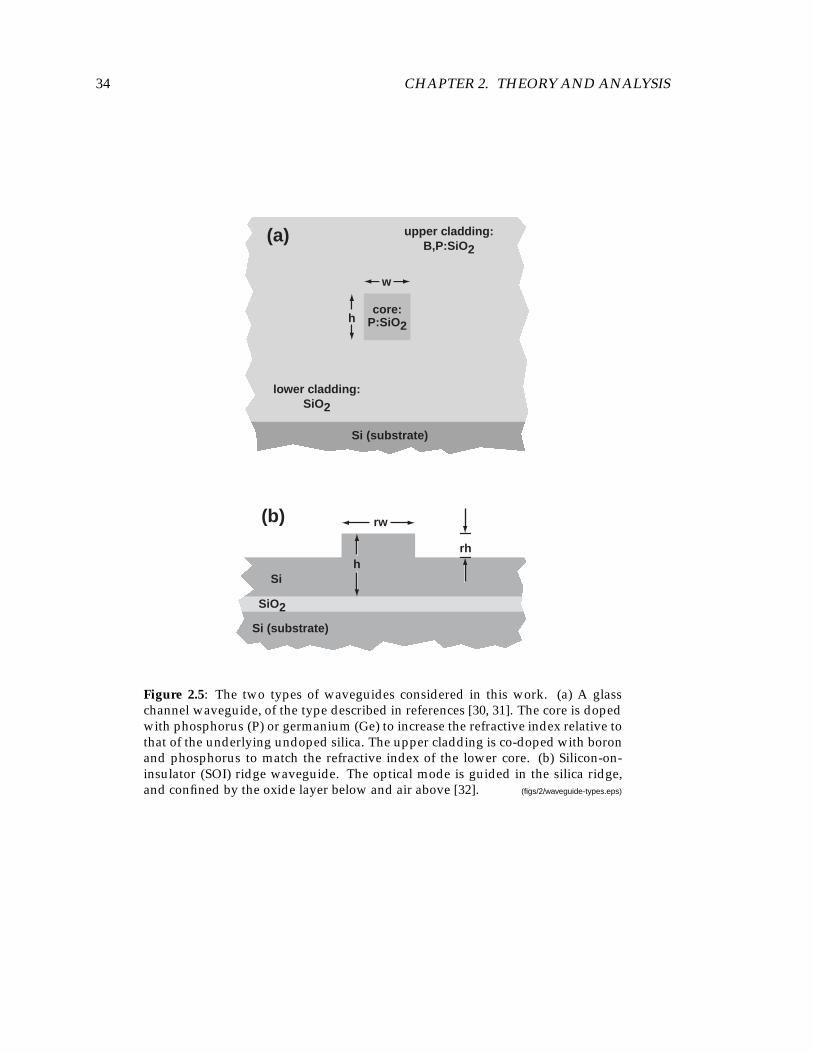
The two types of dielectric waveguides considered in this work are illustrated in Fig. 2.5.The first is a doped-glass channel waveguides, whose index profile and mode shape aredesigned to match well with that of an optical fiber [30, 31]. The second type of waveguidethat will be analyzed is a silicon-on-insulator (SOI) ridge waveguide [32, 33].
The doped-glass waveguide consists of a rectangular core region surrounded by acladding region with slightly lower index of refraction. The lower cladding layer is fusedsilica (SiO2). By doping the core region with phosphorus or germanium, the index of re-fraction can be raised slightly with respect to the underlying silica. The top cladding layeris co-doped with both boron and phosphorus in order to match the refractive index of thelower cladding. The index contrast for this type of waveguide typically ranges from 0.3%to 0.8%, and can be adjusted by varying the dopant concentration in the core layer. Fig-ure 2.6 plots the calculated mode profile for a Ge-doped glass channel waveguide withan index contrast of 0.8%. The waveguides measure six microns on each side, which in-sures that the structure only supports one bound mode for each polarization state. Noticethat because of the rectangular symmetry of the structure, only one quadrant of the modeneeds to be included in the calculation.
In the silicon-on-insulator ridge waveguide, the light is confined in the silicon ridgestructure which sits on top of an oxide separation layer. Provided the oxide layer is thickenough, the light will remain confined in the silicon layer without escaping into the siliconsubstrate. By choosing the ridge height appropriately, the structure can be made to haveonly one bound mode per polarization state, even for relatively large mode sizes [34, 35].Because the structure requires no top cladding layer (the air above the waveguide formsthe top cladding), this structure avoids some of the challenging problems of material over-growth. Figure 2.7 plots the calculated mode profiles for an SOI ridge waveguide. For thisstructure, the core height is 3 µm, and the ridge width is 4 µm.
2.2 Coupled Waveguides
In the preceding section, we described techniques for describing the modes of propagationfor an optical waveguide. In analyzing the waveguide, we assumed that the structure canbe described by a z-invariant refractive index profile n(x, y) which extends infinitely inthe transverse directions. Such a waveguide performs no real optical function except totransmit a light signal from one point to another. In this section, we investigate a slightly
34 CHAPTER 2. THEORY AND ANALYSIS
Si
Si (substrate)
SiO2
rw
rhh
h
w
Si (substrate)
upper cladding:B,P:SiO2
P:SiO2core:
lower cladding:SiO2
(b)
(a)
Figure 2.5: The two types of waveguides considered in this work. (a) A glasschannel waveguide, of the type described in references [30, 31]. The core is dopedwith phosphorus (P) or germanium (Ge) to increase the refractive index relative tothat of the underlying undoped silica. The upper cladding is co-doped with boronand phosphorus to match the refractive index of the lower core. (b) Silicon-on-insulator (SOI) ridge waveguide. The optical mode is guided in the silica ridge,and confined by the oxide layer below and air above [32]. (figs/2/waveguide-types.eps)

2.2. COUPLED WAVEGUIDES 35
-5dB -10dB -15dB -20dB -25dB 30dB
0 1 2 3 4 5 6 7 8 9
9
0
1
2
3
4
5
6
7
8
y(µ
m)
x(µm)
SiO2n = 1.46
dopedSiO2
∆n/n = 0.8%
∆x = ∆y = 0.05 µmnx = 180, ny = 180
Parameters:
λ0 = 1550 nm
TE Mode (ex plotted)neff = 1.46645
3 µm
Figure 2.6: Mode profile for an integrated channel waveguide in silica. For thesimulation, the index contrast was taken to be 0.8%, which could be achieved bydoping the core of region with germanium. The dimensions of the waveguideare 6 µm × 6 µm. Plotted here is the transverse electric field component ex for thefundamental TE mode. The orthogonal field component ey (not plotted) is approx-imately 30-40 dB lower than ex. Note that because of the rectangular symmetry ofthe waveguide, only one quadrant was included in the computational window.The fundamental TE and TM modes are degenerate, because the waveguide isperfectly square. (figs/2/glass-wg-modeprofile.eps)

36 CHAPTER 2. THEORY AND ANALYSIS
2 µm
1 µm
air
Si
SiO2
n = 1
n = 3.63
n = 1.46
2 µm
00
1
2
3
4
5
0
1
2
3
4
5
1 2 3 4 5 6 7
TM Mode (ey plotted)neff = 3.61764
TE Mode (ex plotted)neff = 3.61842
-5dB
-5dB
-10dB
-10dB
-20dB
-20dB
-30dB
-30dB
-40dB
-40dB
y(µ
m)
y(µ
m)
x(µm)
∆x = ∆y = 0.05 µmnx = 140, ny = 100
λ0 = 1550 nm
Figure 2.7: Mode profile for an integrated silicon-on-insulator (SOI) ridge wave-guide. The upper portion of this plot depicts the principal field component exfor the fundamental TE mode of the structure, and the lower portion of the plotdepicts the principal field component ey for the TM mode of the structure. (figs/2/soi-
wg-modeprofile.eps)

2.2. COUPLED WAVEGUIDES 37
Input P1
P2
L
Figure 2.8: The structure of a typical integrated directional coupler. Two wave-guides, initially separated, are brought together so that power may transfer fromone to the other. The path of approach and length of interaction must be carefullyengineered to achieve the desired amount of power transfer. (figs/2/simple-coupler-
schematic.eps)
more complicated structure consisting of two (or more) interacting waveguides in closeproximity. Such a structure, which we call a waveguide coupler, performs the importanttask of transferring light from one waveguide to another. Waveguide couplers are impor-tant components in Mach-Zehnder interferometers, power splitters, and a variety of otherintegrated optical devices.
Figure 2.8 illustrates schematically the type of structure which we wish to describe.Two waveguides, labeled 1 and 2, which are initially separated are slowly brought closeto one another over some interaction length L. The waveguide separation and interactionlength must be selected in order to achieve the desired amount of power transfer.
2.2.1 Variational Approach
We begin by simplifying the problem to the analysis of two parallel waveguides, as de-picted in Fig. 2.9, ignoring for the moment the gradual approach and separation at eitherend of the device. We shall denote the electromagnetic modes of waveguides 1 by e1 andh1, and those of waveguide 2 by e2 and h2.
n21(x, y) → e1(x, y), h1(x, y)
n22(x, y) → e2(x, y), h2(x, y) ,
(2.46)

38 CHAPTER 2. THEORY AND ANALYSIS
where n1(x, y) denotes the index profile of waveguide 1 in the absence of waveguide 2,and n2(x, y) is the index profile of waveguide 2 in the absence of waveguide 1.
Next, we attempt to describe the electromagnetic fields of the coupled waveguide sys-tem as a superposition of the modes of waveguides 1 and 2.
E(x, y, z) = a1(z)e1(x, y) + a2(z)e2(x, y)
H(x, y, z) = a1(z)h1(x, y) + a2(z)h2(x, y)(2.47)
In the above equation, a1(z) and a2(z) are scalar functions of zwhich represent respectivelythe mode amplitude in waveguide 1 and the mode amplitude in waveguide 2. When thetwo waveguides are very far apart, i.e. when d is large compared to the mode size, thetwo optical modes should propagate independently without interaction as described inSection 2.1. In this case, the solution for ai(z) is:
a1(z) = a1(0) exp(−jβ1z)
a2(z) = a2(0) exp(−jβ2z)(2.48)
Eq. 2.48 can be viewed as the solution to the following differential equation:
d
dz
[a1(z)a2(z)
]=
[−jβ1
−jβ2
][a1(z)a2(z)
](2.49)
The goal of this section is to derive a new differential equation which describes the evolu-tion of a1(z) and a2(z) when the two waveguides are brought close together. Essentially,we seek to replace Maxwells equations by a system of two coupled differential equationsfor the scalar mode amplitudes. This analysis comes under the rubric of coupled modetheory[36].
Before proceeding, we should point out that the mode expansion of Eq. 2.47 is onlya convenient approximation. While for a single isolated waveguide, the electromagneticfields may be accurately described as a superposition of the orthogonal modes, the modesof the two constituent waveguides in a coupler do not comprise an orthonormal basis set.Nevertheless, it seems reasonable to use the expansion of Eq. 2.47 as a trial function. Amore rigorous analysis of the waveguide coupler will be presented in Section 2.2.2.
One of the most complete methods for analyzing coupled waveguides is the variationalapproach described in reference [37], which we summarize here. The variational method

2.2. COUPLED WAVEGUIDES 39
n2(x,y)
n1(x,y)2
n2(x,y)
2
(a)
(b)
(c)
d
Figure 2.9: (a) Cross-sectional diagram of two parallel waveguides (ridge wave-guides in this example) separated by a center-to-center distance d. (b) Refractiveindex profile for waveguide 1 in the absence of waveguide 2. (c) Refractive indexprofile for waveguide 2 in the absence of waveguide 1. (figs/2/parallel-waveguides.eps)

40 CHAPTER 2. THEORY AND ANALYSIS
begins with an integral expression for the propagation constant β.
β =
j
4
∫∫ (∇t × h− jk
η0n2e) · e∗ − (∇t × e − jkη0h) · h∗
dx dy
14
∫∫(et × h∗
t + e∗t × ht) · z dx dy(2.50)
In the above equation, the integration is performed of the entire x-y plane, and n2 refersto the complete refractive index profile, including both waveguides. The fields e and h
and propagation constant β likewise refer to the eigenmodes of the coupled waveguidesystem considered as a whole. (Note that we have assumed a z-dependence of e−jβz forthe field quantities of Eq. 2.50.) Of course, we could apply the techniques of Section 2.1to rigorously solve for the modes of the aggregate structure, but for now, we will treat thequantities e, h and β as unknown eigenmodes which we wish to approximate in terms ofthe modes of the constituent waveguides considered separately.
As shown in [37], Eq. 2.50 is a variational expression for the propagation constant β.This means that if the electromagnetic fields e and h are perturbed slightly, i.e.,
e → e + δe
h → h+ δh, (2.51)
the value of the integral of Eq. 2.50 changes only to second-order in δe and δh.
β → β +∫∫ [
α2|δe|2 + γ2|δh|2] dx dy (2.52)
Therefore, one way to determine the two fields e and h is to find the two vector functionswhich minimize the value of the integral given in Eq. 2.50. 2
Clearly, it is unreasonable to minimize Eq. 2.50 over all continuous vector functions ofx and y. In the variational approach, we instead perform a constrained minimization inwhich we assume that the fields e and h are described by the superposition of the isolatedwaveguide modes.
e(x, y) = a1e1(x, y) + a2e2(x, y)
h(x, y) = a1h1(x, y) + a2h2(x, y)(2.53)
The above equation is idential to Eq. 2.47 except that we have factored out the e−jβz de-pendence from E, H, and ai(z). We have added a tilde to the fields e and h to distinguish
2In fact, a similar minimization principle forms the basis for all finite-element mode solvers [17, 38].

2.2. COUPLED WAVEGUIDES 41
them from the exact solutions e and h. Rather than minimizing Eq. 2.50 over the space of allcontinuous functions, we instead minimize over a two-dimensional subspace consisting ofall possible linear combinations of the two isolated waveguide modes.
We shall use β to denote the minimal value achieved by Eq. 2.50 under the linearsuperposition constraint. This optimal value should closely approximate the real prop-agation constant β of the coupled waveguide structure. Likewise, the fields which mini-mize Eq. 2.50 should closely approximate the actual electromagnetic mode of the aggregatestructure:
β β, e e, h h (2.54)
In fact, the error between the actual fields e and h and the optimal linear superposition eand h can easily be shown to be orthogonal to any function in the subspace over which theminimization is performed. (By “orthogonal”, we refer to the inner product described inEq. 2.31.)
If the trial functions of Eq. 2.53 are substituted into Eq. 2.50, the resulting integral ex-pression for β can be cast into the following form:
β =a†Haa†Pa
, (2.55)
where a is a two-dimensional vector of mode amplitudes and H and P are Hermitianmatrices defined below.
a =
[a1
a2
](2.56)
Pij =14
∫∫(ej × h∗
i + e∗i × hj) · z dx dy (2.57)
Hij = Pijβj +k
4η0
∫∫ [(n2 − n2
j)ej · e∗i]dx dy (2.58)
All of the integrals in the above equations are taken over the entire x-y plane. However,notice that the integrand involved in Hij vanishes for points outside of waveguide i andtherefore the range of this integral may be restricted to waveguide i.
Minimizing Eq. 2.55 with respect to the two components of a leads to the followingequation:
βPa = Ha . (2.59)

42 CHAPTER 2. THEORY AND ANALYSIS
The above equation can be seen to be a generalized eigenvalue equation, with eigenvectorsa. Because we know that β describes the propagation constant of the fields, we can obtainthe coupled mode equations by simply replacing β with j d
dz in Eq. 2.59:
[P11 P12
P21 P22
]d
dz
[a1(z)a2(z)
]= −j[H11 H12
H21 H22
][a1(z)a2(z)
]. (2.60)
Eq. 2.60 is a coupled two-dimensional linear differential equation which describes theevolution of the coefficients a1(z) and a2(z) for the parallel waveguide system. The diag-onal elements of P represent the modal power carried by each of the two isolated wave-guide modes separately. The off-diagonal elements of P describe the extent to which thetwo isolated waveguide modes are not orthogonal to each other.
We will now examine the solution to this system of equations, in the case where the twowaveguides under consideration are identical (we shall let β1 = β2 ≡ β0). For identicalwaveguides, Eq. 2.60 can be cast into the following form:
[1 x
x 1
]d
dz
[a1(z)a2(z)
]= −j[
1 x
x 1
][β0 00 β0
]+
[∆ µ
µ ∆
][a1(z)a2(z)
](2.61)
where the constants x, ∆, and µ are defined by,
x ≡ 14P
∫∫(e1 × h∗
2 + e∗2 × h1) · z dx dy (2.62)
∆ ≡ 14Pk
η0
∫∫guide 2
e1 · e∗1 dx dy (2.63)
µ ≡ 14Pk
η0(n2
core − n2clad)∫∫
guide 1/2
e1 · e∗2 dx dy (2.64)
By inverting the matrix on a left-hand side of Eq. 2.61, the coupled mode equations sim-plify to:
d
dz
[a1(z)a2(z)
]= −j[β′0 µ′
µ′ β′0
][a1(z)a2(z)
], (2.65)

2.2. COUPLED WAVEGUIDES 43
where the quantities β ′0 and µ′ are given by
β′0 ≡ β0 +∆− µx1− x2
(2.66)
µ′ ≡ µ− x∆1− x2
(2.67)
Notice that the diagonal elements of the Jacobian matrix in Eq. 2.65 are not equal to β0,the propagation constant of the isolated waveguides. This means that the presence of thenearby waveguide in fact changes the propagation constant slightly.
Eq. 2.65 can easily be solved by eigenvalue decomposition. The solution for a1(z) anda2(z) can be written as a transfer matrix:
[a1(z)a2(z)
]= ejβ
′0z
[cos(µ′z) −j sin(µ′z)
−j sin(µ′z) cos(µ′z)
][a1(0)a2(0)
](2.68)
If, at z = 0 light is launched into waveguide 1, the relative power in the two waveguidesas a function of z is: ∣∣∣∣a2(z)a1(0)
∣∣∣∣2
= sin2(µ′z),∣∣∣∣a1(z)a1(0)
∣∣∣∣2
= cos2(µ′z) . (2.69)
The above equation illustrates the fact that for two coupled identical waveguides thepower slowly sloshes back and forth between them at a rate described by µ ′. Interestingly,full power transfer from waveguide 1 to waveguide 2 can be achieved even for weaklycoupled waveguides (with arbitrarily small µ′), provided the interaction length z is suffi-ciently long.
Henceforth, we will drop the prime from the quantities β ′0 and µ′ in Eq. 2.68. We referto µ as the “coupling constant” for the structure. It has dimensions of inverse length, anddescribes the spatial rate at which power transfers between the two waveguides.
2.2.2 Exact Modal Analysis
In Section 2.2.1, we described a variational technique in which we approximated the elec-tromagnetic fields of the parallel waveguide system in terms of a linear superposition ofthe modes of each constituent waveguide. In principle, it is possible to rigorously com-pute the electromagnetic modes for the coupled waveguide system using the techniquesdescribed in Section 2.1.

44 CHAPTER 2. THEORY AND ANALYSIS
The variational technique gives valuable insight into the structure of the eigenmodesfor the coupled waveguide system. If we consider the case of identical waveguides, theeigenvalue equation (Eq. 2.59) simplifies to:
[β0 µ
µ β0
][a1
a2
]= β
[a1
a2
], (2.70)
where the quantities β0 and µ are defined in Eqs. 2.66 - 2.67 and β represents an eigenvalueof the system of equations. The eigenvalues and corresponding normalized eigenvectorsof this equation are,
βs = β0 + µ, as =1√2
[+1+1
](2.71)
βa = β0 − µ, aa =1√2
[+1−1
](2.72)
Thus, the approximate eigenmodes of the coupled waveguide system are symmetric andantisymmetric linear combinations of the isolated waveguide modes. 3 The symmetricmode has a propagation constant which is slightly higher than the antisymmetric mode.This gives rise to another physical interpretation of the coupling constant µ: µ describes thesplitting between the symmetric and antisymmetric modes of propagation for the parallelwaveguide system.
µ =12(βs − βa) (2.73)
In fact, a more rigorous way to analyze the coupling between parallel waveguides isto directly compute the symmetric and antisymmetric modes. Figure 2.10 illustrates thesymmetric and antisymmetric TE modes for two coupled SOI ridge waveguides, of thetype depicted in Fig. 2.7.
The coupled mode theory presented earlier agrees very well with the more rigorous di-rect solution method described here, especially when the waveguide separation becomeslarge [39]. Moreover, the coupled mode approach has a few advantages over directly solv-ing for symmetric and antisymmetric modes. One limitation of the direct solution methodis that the simulations must be repeated if the waveguide separation changes. For the
3If the two waveguides comprising the coupler are not identical, then the eigenmodes of the coupled sys-tem will not have definite symmetry. Nevertheless, the two lowest order modes may be approximated bylinear combinations of the isolated waveguide modes according to the eigenvalue equation.

2.2. COUPLED WAVEGUIDES 45
0
0
1
2
3
4
5
1 2 3 4 5 6 7 8 9 10
y(µ
m)
0
1
2
3
4
5
y(µ
m)
x(µm)
air
Si
SiO2
n = 1
n = 3.63
n = 1.46
Symmetric TE Mode (ex plotted)neff = 3.61855
Antisymmetric TE Mode (ex plotted)neff = 3.61829
λ0 = 1550 nm
3 µm
1 µm
2 µm
4 µm
∆x = ∆y = 0.05 µmnx = 200, ny = 100
-5dB-10dB -20dB
-30dB
-40dB
-5dB-10dB -20dB -30dB
-40dB
Figure 2.10: Symmetric and antisymmetric TE modes for an SOI ridge waveguide.Note that because of the symmetry, only half of the structure needs to be includedin the computation. (figs/2/symmetric-antisymmetric.eps)

46 CHAPTER 2. THEORY AND ANALYSIS
coupled mode approach, the isolated waveguide mode only needs to be computed once– different waveguide separations can be analyzed by simply changing the regions of in-tegration for the calculation. Also, the direct calculation of symmetric and antisymmetricmodes proves to be numerically challenging as the waveguide separation increases. Themethod relies on accurately computing the difference between two similar propagationconstants (βs and βa), which leads to numerical inaccuracies when the two numbers aresubtracted. By contrast, the coupled mode approach computes the coupling constant µ byway of an overlap integral which is not susceptible to these problems.
2.2.3 Real Waveguide Couplers
Thus far, we have discussed the problem of parallel waveguides without considering thegradual approach and separation of the two waveguides at the input and output of thecoupler. Because most waveguides cannot be bent at a sharp angle without incurring sig-nificant loss, any realistic coupler must include a gradual approach and separation. Inorder to design a coupler with the desired splitting ratio, one must account for the powertransfer which occurs in these curved regions.
If the bending of the waveguide is very gradual in comparison to the coupling rate,i.e., if the waveguide separation changes slowly over a length scale of 1/µ, the effectsof bending may be modeled by simply replacing µ by µ(z) in Eq. 2.68. This conditionis known as the adiabatic condition. In this case, the solution to the coupled system ofdifferential equations is:
[a1(z)a2(z)
]= ejβ0z
[cosφ(z) −j sinφ(z)
−j sinφ(z) cosφ(z)
][a1(0)a2(0)
](2.74)
φ(z) ≡∫ z
0µ(z) dz (2.75)
The above equation is identical to Eq. 2.68, with the exception that µz has been replacedby an integral over the length of the coupler.
A more rigorous analysis of the problem of nonparallel waveguides is given in refer-ences [40, 41, 42]. The authors show that when the waveguide dimensions or separationchange with position, the couple mode equations of Eq. 2.60 should be replaced by thefollowing modified differential equation:
Pdadz
+12dPdz
a = −jHa (2.76)

2.2. COUPLED WAVEGUIDES 47
θ
R
d0
z
x
slope = tan(θ)
d(z)
L0
Figure 2.11: Schematic of a more realistic directional coupler, in which two identi-cal waveguides approach each other over a curved path with radius R. (figs/2/real-
coupler-schematic.eps)
where the matrices P and H are the same as those described earlier, but they are nowunderstood to be slowly varying functions of z. Most couplers have a plane of symmetrysuch that with the proper choice of origin the elements of P and H are even functions of z.In this case, the dP
dz terms are odd functions of z and therefore integrate to zero when theentire coupler is considered. Therefore, provided the structure is symmetric, Eq. 2.74 canbe used to describe the coupling.
Figure 2.11 depicts the geometry of a typical integrated waveguide coupler. Two wave-guides initially approach each other along a sloped path. The waveguides gradually be-come parallel as they traverse an arc of radius R and angle θ, and remain parallel for alength L0. Then, the waveguides gradually separate, following a symmetric path. Fig-

48 CHAPTER 2. THEORY AND ANALYSIS
L0
d0
z0 z1-z0-z1
d(z)
z
Rsin(θ)
d0 + 2R(1 - cos θ)
Figure 2.12: Waveguide center-to-center separation as a function of z for the cou-pler depicted in Fig. 2.11. (figs/2/d-vs-z.eps)
ure 2.12 plots the waveguide separation as a function of separation d for this structure.The waveguide separation can be described mathematically by the following piecewisefunction:
d(z) =
d0 |z| < L0
2
d0 + 2R− 2√R2 − (|z| − L0
2
)2 L02 < |z| < L0
2 +R sin θ
d0 + 2R(1− cos θ) + 2(|z| − L0
2 −R sin θ)tan θ L0
2 +R sin θ < |z|(2.77)
For the purposes of this analysis, we assume that d(z) continues to grow linearly to ∞outside of the coupling region. In practice, the coupling constant µ becomes negligiblysmall as the waveguide separation increases and therefore the exact functional form ofd(z) outside of the principal coupling region is unimportant.
One way to treat the structure depicted in Fig. 2.11 is to simply compute the integratedcoupling numerically, using Eq. 2.75 along with the calculated coupling constants as afunction of d. For example, the coupler may be divided into short segments over whichthe coupling is approximately constant, and then the integral of Eq. 2.75 could be approx-imated by a discrete summation.
However, as described below, by making a few simplifying assumptions, one can de-

2.2. COUPLED WAVEGUIDES 49
rive a simple analytical approximation for the total integrated coupling.
In most cases, the coupling constant µ falls exponentially with increasing waveguideseparation d. This occurs because the electromagnetic mode decays exponentially outsideof the core, and therefore so does the overlap integral of Eq. 2.64. It is often very accurateto model this relationship with the following simple functional form [39, 30]:
µ(d) = A exp(d
d
), (2.78)
where the coefficient A represents the extrapolated coupling at d = 0, and d represents the1/e decay length.
Next, we assume that the waveguide separation in the non-parallel regions can be mod-eled as a quadratic function:
d(z) d0 |z| < L0
2
d0 +1R(z − L0
2)2 L0
2 < |z|(2.79)
The above equation can be derived by simply performing a Taylor expansion of Eq. 2.77.When this approximation is combined with the exponential decay approximation of Eq.2.78, the total integrated coupling can be computed analytically:
∫ +∞
−∞µ(z) dz = µ(d0)
(L0 +√πdR)
(2.80)
Thus, under certain conditions, the coupling between the two non-parallel waveguidescan be treated as if the coupler were comprised of two parallel waveguides separated byd0 with an effective coupling length given by
Leff = L0 +√πdR (2.81)
as described in [39], this approximation is valid under the following condition:
R
dsin2 θ 1 (2.82)
2.2.4 Results of Coupled Mode Analysis
Figure 2.13 plots the coupling constant µ as a function of waveguide separation d for thedoped-glass channel waveguide structure considered in this work. Notice that the rela-

50 CHAPTER 2. THEORY AND ANALYSIS
tionship between µ and d is approximately exponentially decreasing, as evidenced by thelinear slope of the curves when plotted on semilogarithmic axes. There is a slight deviationfrom the exponential decay when the waveguides are very close together.
Also, it is worth pointing out that there is a slight discrepancy between the TE and TMcoupling constants, but the difference is too small to be visible in Fig. 2.13.
Figure 2.14 plots the coupling constant µ as a function of waveguide separation for thesilicon-on-insulator ridge waveguide considered in this work. Notice that because of thestronger index contrast between the core and cladding, the SOI waveguide has a muchmore severe polarization dependence than the doped-glass channel waveguide.
2.2.5 Design of Insensitive Couplers
So far, we have described the coupling between parallel waveguides, and explained howto accurately treat the coupling between nonparallel waveguides. Together with the eigen-mode analysis of Section 2.1, these techniques allow one to design an integrated couplerwith the desired power splitting ratio. However, these calculations can only accuratelypredict the coupling at one specific wavelength and for one polarization state. If thewavelength and polarization change, the eigenmodes of the waveguides also change, andtherefore so does the coupling constant µ. It is often impossible to achieve broadbandpolarization-insensitive performance, especially in planar integrated devices.
Figure 2.15 depicts the calculated power splitting ratio for an integrated glass wave-guide coupler, as a function of wavelength. This particular coupler was designed to havea power splitting ratio of 50% at a free-space wavelength of 1550 nm, but over a span of100 nm the calculated coupling varies from 40 to 60%.
Even in applications where the wavelength and polarization are well-defined and care-fully controlled, small deviations or nonuniformities in the fabrication process, materialproperties, or device operating conditions can significantly alter the power splitting ratio.
We now describe an improved design for a directional coupler which yields a powersplitting ratio that is insensitive to wavelength, polarization, and fabrication parameters.
Others have achieved wavelength-insensitive performance by using tapered wave-guide couplers [43, 44] or asymmetric waveguide couplers [45, 46, 47]. Although theseapproaches can greatly reduce the wavelength dependence, they do not explicitly accountfor polarization and fabrication uncertainties. Another approach to achieving insensitive

2.2. COUPLED WAVEGUIDES 51
10-2
10-3
10-4
10-5
10-6
6 8 10 12 14 16 18 20
TE/TM
d (µm)
µ (
µm
-1)
Figure 2.13: Coupling constant µ(z) as a function of d for a doped-glass channelwaveguide. These data were calculated using the variational theory describe ear-lier. (figs/2/mu-vs-d-glass.eps)

52 CHAPTER 2. THEORY AND ANALYSIS
4 4.5 5 5.5 6 6.5 7 7.5 8 8.5 9
10-2
10-3
10-4
10-5
TE
TM
d (µm)
µ (
µm
-1)
Figure 2.14: Coupling constant µ(z) as a function of d for an SOI ridge waveguide(figs/2/mu-vs-d-soi.eps)

2.2. COUPLED WAVEGUIDES 53
1500 1520 1540 1560 1580 160035
40
45
50
55
60
65
wavelength (nm)
Po
wer
Sp
litti
ng
Rat
io (
%)
Figure 2.15: Calculated splitting ratio as a function of wavelength for an integrateddoped-glass waveguide coupler. The coupler was designed to have a power split-ting ratio of 50% at a free-space wavelength of 1550 nm. (figs/2/coupler-dispersion.eps)

54 CHAPTER 2. THEORY AND ANALYSIS
φ1
φ2
2θ
Figure 2.16: Structure of a parameter-insensitive directional coupler: two con-ventional couplers are cascaded in a Mach-Zehnder configuration, with a relativephase shift introduced between them. (figs/2/mz-coupler-structure.eps)
performance is to use adiabatic couplers [48], but this approach can require very longstructures, and the application to couplers with arbitrary splitting ratio is not obvious.
Another method for achieving wavelength insensitive performance is to use a cascadeof two similar couplers in a Mach-Zehnder configuration [49, 50, 51]. Using numerical opti-mization techniques in combination with empirically determined wavelength-dependencedata, researchers at NTT have employed this technique to build broadband 20% couplers[51]. By contrast, we describe here a simple set of universal design rules for constructingparameter-insensitive cascaded couplers with any desired splitting ratio.
Figure 2.16 depicts the structure of the parameter-insensitive coupler. The device con-sists of a cascade of two conventional couplers, with an intervening phase shift. The di-mensionless quantities φ1 and φ2 represent the total integrated coupling of the two con-stituent directional couplers,
φ1 ≡∫(1)
µ(z) dz, φ2 ≡∫(2)
µ(z) dz (2.83)
and 2θ is the relative phase difference between the two arms of the structure. This phaseshift can be achieved by making one arm slightly longer than the other, or through someother thermo-optic or electro-optic effect.
The cascaded coupler depicted in Fig. 2.16, can be analyzed using a transfer matrixapproach, which will be described completely in Section 2.4. For now, we will simply givethe result for the power splitting ratio. The splitting ratio, defined as the fractional amount

2.2. COUPLED WAVEGUIDES 55
of power transferred from guide 1 to guide 2, is given by [52, 51]:
S = cos2 θ sin2(φ1 + φ2) + sin2 θ sin2(φ1 − φ2) (2.84)
each of the three parameters used in Eq. 2.84 implicitly depends on the wavelength, polar-ization, material properties and dimensions of the device. However, the deviations in φ1
and φ2 are usually highly correlated with each other. By connecting the couplers with anappropriate phase shift, these variations can be made to counteract each other such thatthe resulting power splitting ratio remains unchanged.
Compared with other methods of achieving wavelength-insensitive performance, thisapproach has the advantage that it is easily adaptable to any waveguide geometry. Ratherthan attempting to numerically model the coupling dispersion or polarization dependence,as was done in reference [51], this technique instead treats all potential variations as frac-tional changes in φ1 and φ2. Accordingly, the device should be capable of compensatingfor any uncontrolled variation (structural or optical) which affects both constituent cou-plers proportionately. The variations in φ1 and φ2 tend to be more severe than variationsin θ because of the evanescent nature of the waveguide coupling.
As described in a previous work [52], insensitive performance can be achieved bychoosing the three parameters in the following way:
φ1 =3π8
(1 +
1N
), φ2 =
3π8
(1− 1N
)(2.85)
cos2 θ = sin(
3π2N
)[N + sin
(3π2N
)]−1
(2.86)
where N is a dimensionless real parameter larger than 3 which can be chosen to give anydesired splitting ratio as described in (2.84). Figure 2.17 shows how to select the threeparameters in order to achieve a prescribed splitting ratio. In the particularly importantcase where 50% splitting is desired, we choose φ1 = π/2, φ2 = π/4, and θ = π/3.
Figure 2.18 illustrates how the coupler compensates for fractional changes in φ1 andφ2. For these calculations, φ1, φ2 and θ were nominally chosen so as to give 50% splitting.Along the y-axis, we plot the actual power splitting ratio as a function of the fractionalchange ∆φ/φ. Clearly, for the cascaded Mach-Zehnder structure, the first order depen-dence of splitting ratio on ∆φ/φ has been eliminated.
Having specified φ1, φ2 and θ, the device structure must be selected to achieve thedesired accumulated coupling and phase shift. This task is no more complicated than the

56 CHAPTER 2. THEORY AND ANALYSIS
0 5 10 15 20 25
Splitting Ratio (%)
θ, φ
1, φ2 (
rad
ian
s)
(deg
rees)
30 35 40 4545
50
55
60
65
70
75
80
85
90
50
π2
π3
π4
φ1
φ2
θ
Figure 2.17: Plot describing how the three dimensionless parameters φ1, φ2 and θof the coupler should be selected in order to achieve insensitive performance forany desired splitting ratio. (figs/2/insensitive-coupler-parameters.eps)

2.2. COUPLED WAVEGUIDES 57
70
65
60
55
50
45
40
35
30-20 -15 -10 -5 0 5 10 15 20
Fractional Change (%)∆φφ
Sp
litti
ng
Rat
io (
%)
π4
π2
2π3
π4
Figure 2.18: Plot comparing a conventional directional coupler to the improvedMach-Zehnder structure. Along the vertical axis, we plot the power splitting ratio,and horizontal axis represents a fractional change in the parameters φ1 and φ2.(figs/2/insensitive-coupler-theory.eps)

58 CHAPTER 2. THEORY AND ANALYSIS
design of a conventional directional coupler.
2.3 Bragg Gratings
In the previous section, we developed a theory to describe the interaction between twocopropagating modes of adjacent waveguides. We now turn to the problem of contradirec-tional coupling, the coupling between forward-traveling and backward-traveling modes.By introducing a periodic modulation in a waveguide, it is possible to create an interactionbetween the otherwise decoupled forward-traveling and backward-traveling modes of anoptical waveguide.
Wave propagation in a periodic medium is a well studied phenomenon in the field ofsolid-state physics. The electronic bandgap which exists in semiconductors arises becausethe electrons move in a periodic medium defined by the crystal lattice. The diffraction ofx-rays by a crystal lattice is another example of wave propagation in a periodic structure[53]. The problem of electromagnetic propagation in a periodic waveguide is a similarphenomenon, with the exception that the light is confined in the transverse directions sothat the interactions occur only in one dimension.
There are many ways to induce a periodic modulation in an integrated waveguide. Insome cases, it is possible to directly modulate the refractive index of the guiding layer,by illuminating the waveguide with ultraviolet light[54, 55, 56], or by utilizing acousto-optical or electro-optical effects. These techniques, however, can only be used in materialswhich have photorefractive, acousto-optic, or electro-optic properties. A more flexible wayof introducing a periodic modulation is to physically corrugate the waveguide structureusing the techniques of lithography and pattern transfer. This is the approach consideredin this thesis.
Before proceeding, let us clarify the relationship between forward-traveling modes andbackward-traveling modes. Recall that the eigenmode equation for an optical waveguide,derived in Section 2.1, has eigenvalues which are β2, the propagation constant squared.Positive values of β correspond to forward-traveling modes, while negative values cor-respond to backward-traveling modes. That the eigenvalue equation depends only uponβ2 seems to indicate that the electromagnetic mode profiles are identical for forward- andbackward-traveling modes. However, the eigenmode equations derived earlier only gov-ern two components of the transverse electromagnetic field. The remaining four field com-ponents can be derived from these two transverse components, but the resulting expres-

2.3. BRAGG GRATINGS 59
sions depend upon the sign of β. The relationship between the n th forward-traveling modeand corresponding backward-traveling mode can be expressed as:
e−nt = ent h−nt = −hnt (2.87)
e−nz = −enz h−nz = hnz . (2.88)
We conventionally use negative subscripts to indicate backward-traveling modes and pos-itive subscripts to indicate forward-traveling modes. It is easy to verify that although thetransverse electric field components are identical for the forward and backward modes,the two modes are orthogonal,
∫∫(e∗+ × h− + e− × h∗
+) · z dx dy = 0 . (2.89)
2.3.1 Bragg Grating Basics
Figure 2.19 depicts the type of structure which we seek to analyze. For most of the exam-ples presented in this chapter, we will consider rectangular grooves etched into the surfaceof an optical waveguide 4, although the analytical techniques can be applied to any peri-odic modulation.
The Bragg grating may be thought of as a one-dimensional diffraction grating whichdiffracts light from the forward-traveling mode into the backward-traveling mode. Thecondition for diffraction into the reverse traveling mode is called the Bragg condition. Inorder for light to be efficiently diffracted in the opposite direction, the reflections fromsubsequent periods of the grating must interfere constructively. This means that the Braggperiod Λ must be related to the free space wavelength λ0 by:
Λ =λ0
2neff, (2.90)
where neff is the effective index of refraction of the structure, which depends upon thematerials comprising the waveguide. Generally speaking, for fiber-optic networks the de-sired operating wavelength is approximately 1550 nm. Table 2.1 lists the appropriate Bragggrating periods for a few common waveguide materials.
Eq. 2.90 assumes that the phase accumulation between reflections from adjacent grat-
4Most lithographic techniques produce gratings with such a rectangular profile, because of the directionaletching processes used.

60 CHAPTER 2. THEORY AND ANALYSIS
Λ
Figure 2.19: A diagram illustrating the type of Bragg grating considered in thiswork. A grating, with spatial period Λ is formed by physically corrugating onesurface of the waveguide. The Bragg grating acts as a one-dimensional diffrac-tion grating which reflects light from forward-traveling mode into the backward-traveling mode. (figs/2/rectangular-grating.eps)
Material Si InP/InGaAsP SiO2
n (refractive index) 3.5 3.17 1.46Bragg grating period Λ 220 nm 245 nm 535 nm
Table 2.1: Bragg periods Λ for some common waveguide materials, assuming afree-space operating wavelength of 1550 nm.

2.3. BRAGG GRATINGS 61
ing teeth is precisely one wavelength. This is the condition for a first-order Bragg grating.It is also possible to utilize higher-order diffraction to couple to the forward and backwardmodes. The more general condition for constructive interference is that the phase accu-mulation between subsequent reflections must be an integral number of wavelengths. TheBragg condition for anmth-order Bragg grating is:
Λ =mλ0
2neff. (2.91)
In this work, we consider only first-order (m = 1) Bragg gratings, because the diffractionefficiency (and hence the contradirectional coupling strength) is generally strongest for thefirst diffracted order. Nevertheless, some people build higher-order Bragg gratings simplybecause the required grating pitch is substantially larger, which simplifies the fabricationprocess.
2.3.2 Contradirectional Coupled Mode Theory
We now turn to the practical question of how to theoretically model a Bragg grating. Themost common way of analyzing Bragg gratings is to use a coupled mode formulation [57,8, 36, 58]. In this approach, the grating is modeled as a small perturbation which producesa coupling between the forward and backward modes of an unperturbed waveguide. Itis important to realize, however, that Bragg grating structures do not have characteristiceigenmodes in the same way that a waveguide does. A better description of the physicsof Bragg gratings is to describe the electromagnetic fields as Bloch waves or Floquet modes,a technique similar to that used to describe electron propagation in a crystal lattice. Afew authors have used this approach to describe wave propagation in a Bragg grating[59, 60, 61]. The analysis of B. E. Little et al. clarifies the relationship between the Floquetanalysis and the more simple coupled mode analysis [60]. There are others who haveanalyzed Bragg gratings using a rigorous full-wave numerical analysis.
Often the periodic modulation in the waveguide can be accurately treated as a smallperturbation of an otherwise z-invariant structure. Figure 2.20 illustrates how a corrugatedwaveguide can be separated into a z-invariant structure with well-defined modes plus aperiodic perturbation. The goal of coupled mode theory is to express the electromagneticfields of the complete structure as a superposition of the fields of the unperturbed wave-guide.
To begin, we shall denote the refractive index profile for the complete structure byn2(x, y, z), and the refractive index profile of the unperturbed waveguide by n2
0(x, y).

62 CHAPTER 2. THEORY AND ANALYSIS
n2(x,y,z) δε(x,y,z)n0(x,y)
ncore2
nclad2
ncore2
nclad2ng
2
z
z
x x x
z z
z z
yyy
yyy
Λ
DΛ (1–D)Λ
2
Figure 2.20: The Bragg grating corrugation may be modeled as a perturbation of anotherwise z-invariant waveguide, as shown in this diagram. n2(x, y, z) representsthe full refractive index profile of the structure, n2
0(x, y) represents the unperturbedz-invariant waveguide, and δε(x, y, z) is the perturbation function. Notice that theperturbation δε(x, y, z) is non-zero only within the grating region. (figs/2/grating-
perturbation.eps)

2.3. BRAGG GRATINGS 63
n2(x, y, z) and n20(x, y) are related by
n2(x, y, z) = n20(x, y) + δε(x, y, z) , (2.92)
where the quantity δε(x, y, z) is a periodic function of z which represents the corrugation.This function is nonzero only within the grating cross-section.
Likewise, we denote the electromagnetic fields of the complete structure by E(x, y, z)and H(x, y, z), and the electromagnetic fields of the unperturbed waveguide by E0 (x, y, z)and H0(x, y, z):
n20(x, y, z) −→ E0(x, y, z), H0(x, y, z) (2.93)
n2(x, y, z) −→ E(x, y, z), H(x, y, z) . (2.94)
The fields E, H, E0, and H0, satisfy Maxwells equations in their respective index profiles,i.e.,
∇× E = −jkη0H ∇× E0 = −jkη0H0 (2.95)
∇× H = jk1η0n2E ∇× H0 = jk
1η0n2
0E0 . (2.96)
Now consider the vector quantity S, defined as
S ≡ E∗0 ×H + E × H∗
0 . (2.97)
Computing the divergence of S, using Eqs. 2.95-2.96 gives
∇ · S = −jkη0δεE∗
0 · E . (2.98)
If we integrate Eq. 2.98 over a volume V , and apply the divergence theorem to the left-handside, we obtain, ∫∫
∂V
S · dA = −jkη0
∫∫∫V
δεE∗0 ·E dV . (2.99)
This relationship is known as the Lorentz reciprocity theorem. The integral on the left-handside is a surface integral, where dA points in the outward direction. If we take the volumeV to be an infinitesimally thin slab of width dz which spans the entire x-y plane, Eq. 2.99

64 CHAPTER 2. THEORY AND ANALYSIS
becomes:
d
dz
∫∫S · z dA = −jk
η0
∫∫δεE∗
0 · E dA , (2.100)
where now both integrals are taken over the x-y plane. To simplify the subsequent analy-sis, we shall use brackets to indicate integration over the x-y plane:
〈f(x, y)〉 ≡∫∫f(x, y) dx dy . (2.101)
At this point, no approximations have been made. The Lorentz reciprocity theorem de-scribed in Eq. 2.100 forms the basis for coupled-mode theory, as we shall describe below.
Now, we attempt to express the electromagnetic fields of the complete structure as alinear superposition of the modes of the unperturbed waveguide.
E(x, y, z) = A+(z)e+(x, y) +A−(z)e−(x, y) (2.102)
H(x, y, z) = A+(z)h+(x, y) +A−(z)h−(x, y) (2.103)
The electromagnetic fields e±(x, y) and h±(x, y) represent the modes of the unperturbedwaveguide at the optical frequency of interest. The goal of coupled mode theory is toreplace Maxwells equations for E and H by a set of coupled ordinary linear differentialequations which describe the evolution of the scalar coefficients A±(z). The Lorentz reci-procity relation of Eq. 2.100 provides the necessary link between the electromagnetic fieldsand the expansion coefficients.
First, let us take E0(x, y, z) and H0(x, y, z) in Eq. 2.100 to be the forward-traveling modeof the unperturbed waveguide, i.e.,
E0(x, y, z) = e+(x, y)e−jβ0z, H0(x, y, z) = h+(x, y)e−jβ0z . (2.104)
Substituting these fields into Eqs. 2.100, along with the mode expansion of Eqs. 2.102-2.103,leads to the following differential equation for A+(z):
d
dzA+(z) = −j
[β0 +
k
4Pη0〈δε e∗+ · e+〉
]A+(z) − jk
4Pη0〈δε e∗+ · e−〉A−(z) , (2.105)
where P denotes the time-averaged power carried by the forward-traveling mode,
P ≡ 14〈(e+ × h∗
+ + e∗+ × h+) · z〉 . (2.106)

2.3. BRAGG GRATINGS 65
A similar equation may be derived for A−(z) by taking E0(x, y, z) and H0(x, y, z) to be thereverse-traveling mode. We omit the details and merely present the result:
d
dzA−(z) = +j
[β0 +
k
4Pη0〈δε e∗− · e−〉
]A−(z) +
jk
4Pη0〈δε e∗− · e+〉A+(z) . (2.107)
Eq. 2.105 and Eq. 2.107 constitute a pair of coupled linear differential equations whichrelate the forward- and backward- mode amplitudes. The terms inside angle brackets aresimple overlap integrals of the mode with the grating perturbation δε. Note, however, thateven though these integrals are taken over the x-y plane, the integrand is proportional toδε, which is a periodic function of z.
The coupled-mode equations can be simplified by expanding δε(x, y, z) as a Fourierseries in z. The Fourier series expansion for δε is:
δε(x, y, z) =∑m
δεm(x, y)e−j2mπz/Λ . (2.108)
Each Fourier coefficient in Eq. 2.108 is a function of x and y only. Eq. 2.108 can be invertedto obtain an expression for the Fourier coefficients in terms of δε(x, y, z):
δεm(x, y) =1Λ
∫ z0+Λ
z0
δε(x, y, z)ej2mπz/Λ dz . (2.109)
Provided the periodic perturbation is real-valued, the Fourier coefficients are related byδε−m = δε∗m.
Substituting the expansion of Eq. 2.108 into the coupled mode equations yields:
d
dzA+(z) = −j
[β0 +
k
4Pη0〈δε0 e∗+ · e+〉
]A+(z)
− jk
4Pη0〈δε1 e∗+ · e−〉e−j2πz/ΛA−(z) + . . .
(2.110)
d
dzA−(z) = +j
[β0 +
k
4Pη0〈δε0 e∗− · e−〉
]A−(z)
+jk
4Pη0〈δε−1 e∗− · e+〉e+j2πz/ΛA+(z) + . . .
(2.111)
In the above equation, we have only retained those terms which are phase-matched. Specif-ically, we have omitted terms from the Fourier expansion which have a spatial periodicitymuch different from the accompanying terms in the equations. For example, when thefunction A−(z) is multiplied by the m = 1 Fourier coefficient, δε1, the resulting product

66 CHAPTER 2. THEORY AND ANALYSIS
has roughly the same periodicity as A+(z). Likewise, when the function A+(z) is multi-plied by the m = −1 Fourier coefficient the resulting function has the same spatial peri-odicity as A−(z). The omitted Fourier expansion terms do not meet the phase-matchingcondition, meaning they oscillate with spatial frequencies which are much different frome±jπz/Λ. When the coupled-mode equations are solved by integrating over z, these rapidly-oscillating terms quickly average to zero, whereas the retained terms do not.
As shown in Eq. 2.110, for a first-order Bragg grating only the m = 0 and m = ±1Fourier coefficients enter into the coupled-mode equations. The m = 0 term induces achange in the propagation constant, i.e. it modifies the diagonal elements of the couplingmatrix, while the m = ±1 terms couple the forward and backward modes. We may castthe coupled mode equations into a simpler form by defining two parameters β and κ, eachinvolving overlap integrals between the unperturbed waveguide modes and the gratingperturbation:
β ≡ β0 +k
4Pη0〈δε0 e∗± · e±〉 (2.112)
κ ≡ − jk
4Pη0〈δε1 e∗+ · e−〉 . (2.113)
With these definitions, the coupled mode equations can be summarized in matrix form:
d
dz
[A+(z)A−(z)
]=
[−jβ κe−j2πz/Λ
κ∗e+j2πz/Λ jβ
][A+(z)A−(z)
]. (2.114)
The magnitude of the complex coupling constant κ describes the rate at which power trans-fers between the forward and backward modes. κ is often described as the “reflectivityper unit length” of the grating. The phase of κ is directly related to the phase of δε1. Fora grating which is symmetric about z = 0, all of the Fourier coefficients will be real, andtherefore κ will be purely imaginary. Even for gratings which do not have this symmetry,the coupled mode equations are of the form given in Eq. 2.114, provided the refractiveindex perturbation is real. 5
By choosing the unperturbed waveguide appropriately, the m = 0 Fourier coefficientcan be eliminated. This is accomplished by choosing n2
0(x, y) to be the z-averaged value of
5If the grating includes a modulation in the optical gain or loss, the perturbation can no longer be modeledby a real-valued function, and the coupled mode equations will be different from those given in Eq. 2.114.[62, 63, 64]

2.3. BRAGG GRATINGS 67
n2(x, y, z):
n20(x, y) =
1Λ
∫ Λ
0n2(x, y, z) dz . (2.115)
It is easy to verify that with this choice, δε0(x, y) = 0, and there is no change in the propa-gation constant as a result of the perturbation.
If we consider the limit as κ → 0, the equations decouple and the solutions for A±(z)are of the form e∓jβz, as expected. Often, it is more convenient to factor out these rapidoscillations fromA±(z) to obtain coupled-mode equations for the slowly-varying envelopefunctions. The rapid oscillations are removed by making the following change of variables:
A±(z) = a±(z)e∓jπz/Λ . (2.116)
With this substitution, the coupled mode equations simplify to
d
dz
[a+(z)a−(z)
]=
[−jδ κ
κ∗ jδ
][a+(z)a−(z)
], (2.117)
where δ is a measure of the deviation from the Bragg condition, given by
δ ≡ β − πΛ
. (2.118)
2.3.3 Spectral Response of Bragg Grating
Bragg gratings are useful because of their frequency-dependent nature. We will now ex-amine this frequency dependence by solving the coupled mode equations which were de-veloped in the previous section.
In the analysis presented earlier, we tacitly assumed that all field quantities were os-cillating at the same optical frequency ω = kc. The quantity β0 and the associated fieldse±, and h± were understood to be the propagation constant and electromagnetic modesfor the unperturbed waveguide at the optical frequency ω. We now asked the question, whathappens when the optical frequency changes?
Strictly speaking, the eigenfunctions and propagation constants must be recomputedusing the new value for k. Then, the overlap integrals in Eqs. 2.112 - 2.113 must be re-computed using the new modes. In order to numerically compute the spectral responsefor a Bragg grating, this process must be repeated for each optical frequency to be consid-

68 CHAPTER 2. THEORY AND ANALYSIS
ered. While this is possible for simple one-dimensional problems, it becomes impracticalfor more realistic waveguides. Fortunately, in most cases the mode profiles do not changesubstantially over the bandwidth of interest. Thus, it is usually sufficient to neglect thesmall change in the electromagnetic modes and simply treat the change in frequency as achange in the propagation constant β. If we Taylor-expand the propagation constant β(ω)to first order about a central frequency ωc, we obtain 6:
β0(ω) = β0(ωc) +dβ0
dω|ωc(ω − ωc)
= β0(ωc) +1vg
(ω − ωc), (2.119)
where vg is the group-velocity of the unperturbed waveguide. Using this relationship,the quantity δ may be expanded to first-order in terms of the deviation from the centralfrequency ωc:
δ(ω) = β(wc)− πΛ +1vg
(ω − ωc) . (2.120)
In the above equation, we have assumed that the unperturbed waveguide geometry hasbeen selected as described in Eq. 2.115 so that there is no first-order change in the prop-agation constant. Usually, the center frequency ωc is chosen to coincide with the Braggfrequency, i.e. β(ωc) = π/Λ, which leads to
δ(ω) =1vg
(ω − ωc) . (2.121)
The expression for the coupling coefficient κ also depends upon ω, both through theelectromagnetic fields which appear in the overlap integrals and through a proportionalityconstant which depends on k(= ω/c). However, these variations are small and can usuallybe neglected over the bandwidth of interest. Therefore, we shall take κ to be a frequency-independent parameter which is calculated at the center frequency ωc.
Thus, we can calculate the spectral response of the Bragg grating by solving the coupledmode equations, treating δ as a variable which measures the deviation from the Braggcondition as described in Eq. 2.121.
The pair of coupled mode equations in Eq. 2.117 comprise a 2 × 2 system of linear
6Notice that to avoid confusion, we had used the subscript c to refer to the central frequency (the opticalfrequency at which the electromagnetic modes were computed.) In contrast, the subscript 0 refers to theunperturbed waveguide geometry.

2.3. BRAGG GRATINGS 69
homogeneous differential equations. The standard technique used to solve such a systemof differential equations is eigenvector decomposition [65]. Applying this technique, thesolution to the coupled mode equations is:
[a+(z)a−(z)
]= [v1 v2]
[eγ1z 00 eγ2z
][v1 v2]
−1
[a+(0)a−(0)
], (2.122)
where v1 and v2 are the eigenvectors of the coupling matrix and γ1 and γ2 are the corre-sponding eigenvalues. The eigenvalues and associated eigenvectors are given by:
γ1 = +γ, v1 =
[γ − jδκ∗
](2.123)
γ2 = −γ, v2 =
[−κγ − jδ
], (2.124)
where the quantity γ is defined as:
γ ≡√
|κ|2 − δ2 . (2.125)
Substituting the eigenvalues and eigenvectors from Eq. 2.123 into Eq. 2.122, we obtain ananalytical solution to the coupled mode equations:
[a+(z)a−(z)
]=
[cosh(γz) − j δγ sinh(γz) κ
γ sinh(γz)κ∗γ sinh(γz) cosh(γz) + j δγ sinh(γz)
][a+(0)a−(0)
]. (2.126)
The above equation gives the solution to the coupled mode equations in transfer matrixform. If the forward and backward mode amplitudes are known at z = 0, they can becalculated at any other location z by simply multiplying by the transfer matrix given anEq. 2.126.
Often, the boundary conditions on a+ and a− at z = 0 are not simultaneously known.Consider, for example, a grating which begins at z = 0 and extends to a length L. Nowimagine injecting light into the left-hand side of the grating. We wish to calculate the re-flection and transmission of the grating. We further assume that no light enters the gratingfrom the right hand side. Substituting these boundary conditions into the transfer-matrixequation gives:
[t
0
]=
[cosh(γL)− j δγ sinh(γL) κ
γ sinh(γL)κ∗γ sinh(γL) cosh(γL) + j δγ sinh(γL)
][1r
], (2.127)

70 CHAPTER 2. THEORY AND ANALYSIS
where r and t represent the reflection and transmission coefficients of the Bragg grating.The second equation in Eq. 2.127 can be directly solved for r, giving:
r(δ) =
κ∗
γtanh(γL)
1 + jδ
γtanh(γL)
, (2.128)
where γ is a function of δ as described in Eq. 2.125. Similarly, the amplitude transmissionfunction t can be shown to be7:
t(δ) =sech(γL)
1 + jδ
γtanh(γL)
. (2.129)
The peak reflectivity of a uniform Bragg grating occurs when δ = 0,
Rmax = |r(δ = 0)|2 = tanh2(κL) . (2.130)
Figure 2.21 plots the calculated reflection spectral response for five different Bragg grat-ings with increasing lengths. From this figure, we can identify two different operatingregimes. When the product κL is small compared to 1, the spectral response of the Bragggratings can be accurately approximated as the Fourier transform of the grating shape.Since the grating begins and ends abruptly and extends for a length L, the spectral re-sponse has a characteristic “sinc” shape whose bandwidth is inversely proportional to thegrating length L. In this limit, the spectral response can be shown to approach:
r(δ) = jκ∗
δsin(δL) . (2.131)
We refer to gratings with κL < 1 as weak Bragg gratings, because in general they onlyreflect a fraction of the incident light. The peak reflectivity in this regime depends uponthe value of κ, but the overall spectral shape and bandwidth is determined only by thegrating length.
A weak Bragg grating does not make a suitable add/drop filter, because it only par-tially reflects the input signal. However, there are cases where the “sinc”-shaped spectralresponse of a weak grating is desirable. In many binary communications systems, the en-coded signal has precisely at the same “sinc”-shaped spectral response. Thus, the weak
7If the transmission function is defined in terms of A± instead of the slowly-varying envelope functionsa±, there is an additional phase term in the expression for t(δ)

2.3. BRAGG GRATINGS 71
-15κ -10κ -5κ 0
1
0.5
0
1
0.5
0
1
0.5
0
1
0.5
0
1
0.5
0
5κδ ( = ∆ω/vg)
|r(δ)
|2|r(
δ)|2
|r(δ)
|2|r(
δ)|2
|r(δ)
|2
10κ 15κ
κL = 0.5(weak bragg grating)
(strong bragg grating)
κL = 1
κL = 2
κL = 4
κL = 8
|r(δ)|2 = |κ|2sin2(δL)
δ2
bandwidth = 2κ
|r(δ = 0)|2 = tanh2(κL)
Figure 2.21: Calculated reflection spectral response from five different Bragg grat-ings, with increasing lengths. (figs/2/kappa-various-l.eps)

72 CHAPTER 2. THEORY AND ANALYSIS
Bragg grating provides a convenient implementation of an all-optical matched filter, whichshould provide the optimal signal-to-noise ratio for detecting the signal in the presence ofwhite background noise [66, 67, 68].
For gratings where the product κL exceeds 1, the spectral response has a plateau-likeshape, as shown in the lower portion of Fig. 2.21. In this regime, the grating has a veryhigh reflectivity within a band of frequencies called the stopband. The spectral width of thestopband is proportional to the grating strength κ:
∆f =κc
πng, (2.132)
where ∆f is the bandwidth and c/ng is the group velocity. Outside of the stopband, thespectral response shows a series of ripples or sidelobes. The sidelobes quickly decay aswe move away from the Bragg condition until the structure is effectively transparent 8.If the grating is made longer without changing the value of κ, the bandwidth remainsunchanged, but the peak reflectivity rises closer to 1, the spectrum becomes more square,and the sidelobes get closer together.
2.3.4 Calculation of Grating Strength
In the previous section, we solved the coupled mode equations to obtain the spectral re-sponse for a Bragg grating. The grating strength κ defines the so-called stopband of theBragg grating, which (for strong gratings) is directly related to the bandwidth of the spec-tral response. We now turn to a more detailed discussion of how this grating strength iscalculated for typical waveguide structures.
As described earlier, we choose the unperturbed waveguide structure such that thereis no 0th Fourier coefficient in the grating perturbation. For a grating comprised of rect-angular teeth with a fixed duty cycle, this means that when constructing the unperturbedwaveguide, the grating should be modeled as a homogeneous slab whose index lies some-where in between the core and cladding indices. We define the duty cycle D to be thefraction of the grating period which is occupied by a tooth of core material. This geometryis illustrated in Fig. 2.20. With this definition, the refractive index profile of the unper-
8In fact, it can be shown that for points well outside of the stopband, the reflectivity of the grating can againbe approximated by Eq. 2.131.

2.3. BRAGG GRATINGS 73
turbed waveguide is:
n20(x, y) =
Dn
2core + (1−D)n2
clad in the grating region
n2(x, y) elsewhere. (2.133)
With this choice, it can easily be verified that δε0(x, y) = 0, as desired. The remainingFourier coefficients can be computed using Eq. 2.109,
δεm(x, y) =
(n
2core − n2
clad)sin(mπD)mπ
in the grating region
0 elsewhere. (2.134)
Note that we have arbitrarily chosen the position of the z = 0 origin to coincide with thecenter of a grating tooth, and consequently all of the Fourier coefficients are real. For first-order Bragg gratings, we are only interested in the first Fourier coefficients. Substitutingthe m = 1 coefficients from Eq. 2.134 into Eq. 2.113, we obtain following equation for thecoupling constant κ:
κ =k
4πPη0(n2
core − n2clad) sin(πD)
∫∫(grating)
e∗+ · e− dx dy . (2.135)
In the above equation, we have omitted the arbitrary phase of κ, recognizing that the phaseis determined by the relative position of the z = 0 origin.
The integrand in Eq. 2.135 can be expanded using the relationships between the for-ward and backward traveling modes given in Eq. 2.87:
e∗+ · e− = |et|2 − |ez|2 (2.136)
The finite difference techniques described in Section 2.1.4 allow one to calculate the trans-verse electric fields et. The longitudinal field component ez and magnetic field h may becomputed from the two transverse components, using Maxwells equations. In most casesof interest, the longitudinal field component is much smaller than the transverse compo-nents, and the equation for κ can be simplified by neglecting the ez terms. In many casesit is also possible to neglect one of the transverse electric field components and simplyuse a semivectorial technique to calculate the principal field component. In the context ofthe semi-vectorial method, the overlap integrals can be re-expressed in terms of one scalarfield quantity representing the principal transverse electric field component (either ex or

74 CHAPTER 2. THEORY AND ANALYSIS
ey),
∫∫(grating)
e∗+ · e− dx dy ∫∫
(grating)
|φ(x, y)|2 dx dy (2.137)
4Pη0 2βk
∫∫|φ(x, y)|2 dx dy , (2.138)
where we have used the symbol φ(x, y) to represent ex for TE modes and ey for TM modes.With this simplification, the expression for the grating strength κ becomes:
κ =k2
2πβ(n2
core − n2clad) sin(πD)Γ . (2.139)
The quantity Γ in Eq. 2.139 is a dimensionless number less than 1 which describes theextent to which the electromagnetic mode overlaps with the grating region.
Γ ≡
∫∫(grating)
|φ(x, y)|2 dx dy∫∫
|φ(x, y)|2 dx dy. (2.140)
Figure 2.22 plots the calculated coupling constant κ as a function of duty cycle D, forvarious grating depths, for the doped glass channel waveguide.
In Fig. 2.23, we plot the coupling constant as a function of duty cycle for various gratingdepths for the silicon-on-insulator ridge waveguide. One interesting effect which is seenin this plot is that the strongest grating strength occurs when the duty cycle is larger than50%. Even though the first Fourier coefficient is maximized by choosing D = 0.5, themode overlap integral increases substantially with duty cycle, leading to the skewed plotspresented in Fig. 2.23. Notice that there is also a significant polarization dependence inthe data presented in Fig. 2.23 – the calculated grating strength for TM-polarized light issubstantially smaller than for TE-polarized light for the same grating edge depth and dutycycle.
Fiber Bragg Gratings
It is instructive to evaluate the strength of a Bragg grating in a waveguide in comparisonto that of a fiber Bragg grating. In a fiber Bragg grating, the periodic modulation is cre-ated by illuminating a photosensitive fiber with a periodic UV standing-wave. Typically,

2.3. BRAGG GRATINGS 75
0 0.1 0.2 0.3 0.4 0.5
gh = 100 nm
gh = 200 nm
gh = 300 nm
gh = 400 nm
gh = 500 nm
0.6 0.7 0.8 0.9 10
0.5
1
1.5
2
2.5
3
3.5
DΛgh
Λ
Duty Cycle (D)
κ (c
m-1
)
0
1
2
3
equ
ivalent ∆
n ( x 10
-4)
κ vs D for TE and TM modes(Doped-Glass Waveguide)
Figure 2.22: Calculated grating strength κ vs. duty cycleD for a doped-glass chan-nel waveguide. The results are indistinguishable for TE and TM polarizations. Thegrating strength is calculated for five different grating etch depths ranging from100 to 500 nm. (figs/2/kappa-glass.eps)

76 CHAPTER 2. THEORY AND ANALYSIS
0 0.1 0.2 0.3 0.4 0.5 0.6
gh = 50 nm
gh = 100 nm
gh = 150 nm
gh = 200 nm
gh = 250 nm
gh = 50 nm
gh = 100 nm
gh = 150 nm
gh = 200 nm
gh = 250 nm
0.7 0.8 0.9 1
0 0.1 0.2 0.3 0.4 0.5
Duty Cycle (D)
0.6 0.7 0.8 0.9 1
0
1
2
3
4
5
6
7
8
9
10
0
1
2
3
4
0
1
2
3
4
5
6
7
8
9
10
κ (c
m-1
)κ
(cm
-1)
DΛgh
Λ
κ vs D for TE modes(SOI Ridge Waveguide)
κ vs D for TM modes(SOI Ridge Waveguide)
0
1
2
3
4
equ
ivalent fib
er ∆n
( x 10-4)
equ
ivalent fib
er ∆n
( x 10-4)
Figure 2.23: Calculated grating strength κ vs. duty cycleD for an SOI ridge wave-guide. The upper plot applies for the TE polarization, while the lower plot corre-sponds to TM polarization. In each case, the grating strength is calculated for fivedifferent grating edges ranging from 50 to 250 nm. (figs/2/kappa-soi.eps)

2.3. BRAGG GRATINGS 77
the fiber core is photorefractive, meaning that its index of refraction can be permanentlychanged by exposing the fiber to UV radiation. In contrast to the integrated Bragg grat-ings discussed so far, a fiber Bragg grating has no physical corrugation – there is simplya small modulation in the refractive index of the core. The amount by which the index ofrefraction can be changed via UV illumination depends upon the composition of the coreand the wavelength of exposure. Many techniques have been developed for enhancingthe photosensitivity of fibers[69], but generally the maximum attainable refractive indexchange in an untreated fiber seldom exceeds 1×10⁻³ [70].
The coupled mode analysis described earlier can also be applied to fiber Bragg gratings.The periodic perturbation δε(x, y, z) for a fiber Bragg grating with a peak-to-peak refractiveindex modulation of ∆n is:
δε(x, y, z) =
n∆n cos(2πz/Λ), inside core
0, outside core, (2.141)
where we have assumed that ∆n/n is small. For the fiber Bragg grating, the periodicperturbation is a pure sinusoid9 which means that the Fourier decomposition of δε(x, y, z)only has two nonzero coefficients:
δε±1 =
n∆n2, inside core
0, outside core. (2.142)
We can now apply the same procedure described earlier for corrugated Bragg gratings,using Eq. 2.142 for the first Fourier coefficient of the grating. The resulting expression forκ is:
κ =k2
4βn∆nΓ , (2.143)
where Γ is, as before, a dimensionless number less than 1, but it now describes the fractionof the modal power which resides in the waveguide core. (In comparison with the cor-rugated Bragg grating, the fiber Bragg can achieve a larger value for Γ because the indexmodulation covers the entire core region.)
For the sake of comparison, we shall evaluate Eq. 2.143 using some values which are
9The sinusoidal index approximation assumes that the UV-induced refractive index change is proportionalto the intensity pattern formed by a superposition of two plane waves of equal amplitude. This is only a con-venient approximation of what really occurs when a fiber Bragg grating is fabricated. Reference [71] describesa technique for measuring the actual refractive index modulation in a fiber Bragg grating.

78 CHAPTER 2. THEORY AND ANALYSIS
typical for the strong fiber Bragg gratings. Specifically, we assume that the peak-to-peakindex modulation amplitude is ∆n = 1×10⁻³, the free-space wavelength is taken to be 1550nm, and the overlap factor Γ is taken to be 90%. With these numbers, the equivalent gratingstrength is approximately κ = 18 cm-1. If we assume that the group index is approximately1.46 (typical for fiber), this corresponds to a stopband spectral width of approximately 120GHz.
2.3.5 Apodized and Chirped Bragg Gratings
So far, we have assumed that the Bragg grating is a perfectly periodic structure whichhas a sharply-defined beginning and endpoint. Often, either by design or because of thefabrication techniques used, the Bragg grating will deviate somewhat from this perfect pe-riodic structure. If the pitch of the Bragg grating changes slowly along the length of thegrating, we say that there is a chirp. More generally, even when the grating is perfectlyperiodic, if the waveguide itself has some slow variation in its propagation constant acrossthe length of the device, the structure will exhibit chirp-like properties. When the ampli-tude of the grating constant κ changes with position, we say that the grating is apodized.In both of these cases, the coupled mode equations must be modified to account for thenonuniformity in the periodic structure. We now describe how to generalize the coupledmode equations to treat apodized and chirped gratings.
First, we recall the coupled mode equations for A±(z) derived earlier for uniform grat-ings. The relevant equations are repeated here for reference:
d
dz
[A+(z)A−(z)
]=
[−jβ κe−jkgz
κ∗e+jkgz jβ
][A+(z)A−(z)
], (2.144)
where kg is the grating spatial frequency, defined by:
kg ≡ 2πΛ
, (2.145)
Now imagine that the grating slowly changes with z. Strictly speaking, the Fourier analy-sis of the grating perturbation no longer applies when the grating is aperiodic. Neverthe-less, provided the grating changes slowly with z, the coupled-mode analysis can still beapplied locally.
The effect of grating apodization can be included by simply letting κ in Eq. 2.144 be aslowly varying function of z. The way to account for grating chirp is to replace the product

2.3. BRAGG GRATINGS 79
kgz by a more general integral∫kg(z) dz. 10 Thus, the generalized coupled mode equations
for nonuniform gratings are:
d
dz
[A+(z)A−(z)
]=
[−jβ(z) κ0(z)e−jφ(z)
κ0(z)∗e+jφ(z) jβ(z)
][A+(z)A−(z)
](2.146)
where φ(z) ≡∫ z
0kg(z′) dz′ . (2.147)
Note: in the above equation, we have also allowed the propagation constant β to varywith z, to account for any slow change in the structure or composition of the waveguideitself, which is indistintuishable from grating chirp. We shall assume that the function κ0
is a real-valued function which describes the magnitude of the grating perturbation. Thegrating phase φ(z) includes all of the information about the chirp and phase of the Bragggrating. For a uniform Bragg grating, this term is a linear function of z, but for nonuniformgratings it not a strictly linear function. The first derivative of φ(z) is the local k-vector ofthe grating.
As before, we often wish to rewrite Eq. 2.146 in terms of the slowly-varying amplitudefunctions a±(z). But now, since there is no well-defined grating periodicity to factor out ofthe equations, we simply choose an arbitrary reference point, βr ,
A±(z) = a±(z)e∓jβrz , (2.148)
Substituting the above equation into the coupled mode equations leads to the followingset of differential equations for the slowly-varying amplitude functions:
d
dz
[a+(z)a−(z)
]=
[−jδ(z) κ(z)κ(z)∗ jδ(z)
][a+(z)a−(z)
], (2.149)
where the functions κ(z) and δ(z) are defined as:
δ(z) = β(z) − βr (2.150)
κ(z) = κ0(z) exp [j(2βrz − φ(z))] . (2.151)
Eq. 2.149 is identical to Eq. 2.117, with the exception that the matrix elements are slowly-varying functions of z. The effect of grating chirp it is to introduce a slow variation inthe phase of κ(z). And the effect of apodization is to introduce a slow variation in the
10One might be tempted to account for grating chirp by simply replacing kg in Eq. 2.144 by a slowly-varyingfunction of z, but this leads to an inconsistent interpretation of kg as the local spatial frequency of the grating.

80 CHAPTER 2. THEORY AND ANALYSIS
magnitude of κ(z).
Because the coefficients of the coupling matrix are no longer constants, the coupledmode equations for nonuniform gratings can no longer be solved in closed form. Thedifferential equation can be solved numerically by simple integration. Again, we are facedwith the problem that the boundary conditions are not completely specified at either endof the structure. For light incident from the left-hand side of the grating, the easiest way tocompute the reflection and transmission coefficients is integrate backwards from right toleft. At the right hand side of the grating, we assume that there is no light impinging fromthe right, and we arbitrarily choose the output amplitude to be 1. Therefore, the boundaryconditions at the end of the grating are:
a(L) =
[a+(L)a−(L)
]=
[10
]. (2.152)
With this as our starting point, we integrate the differential equation from z = L back toz = 0,
a(0) = a(L) +∫ 0
LM(z) a(z) dz , (2.153)
where M(z) is the 2 × 2 coupling matrix in Eq. 2.149. The reflection and transmissioncoefficients are then given by:
r =a−(0)a+(0)
, t =1
a+(0). (2.154)
In Section 2.4, we describe how the numerically computed reflection and transmissioncoefficients can be used to construct the full 2 × 2 transfer matrix for the nonuniformgrating.
If only the reflection coefficient is sought, the problem may be simplified by deriving anew differential equation for the local amplitude ratio r(z), defined as
r(z) ≡ a−(z)a+(z)
. (2.155)
Computing the derivative of Eq. 2.155 with respect to z and using the coupled mode equa-

2.3. BRAGG GRATINGS 81
tions, we obtain the so-called Ricatti differential equation:
d
dzr(z) =
1a+
da−dz
− a−a2+
da+dz
= κ∗(z) + 2jδ(z)r(z) − κ(z)r2(z). (2.156)
As before, this equation can be numerically integrated from right to left to obtain the re-flection coefficient of the Bragg grating.
A simpler approach to the analysis of nonuniform gratings is to simply divide the grat-ing into short segments, over which δ, κ, and Λ are approximately constant. The transfermatrix for the entire structure can then be obtained by simply multiplying the transfer ma-trices for each short segment. Essentially, this technique amounts to performing a prim-itive numerical integration of the differential equations. Transfer matrix methods will befurther discussed in the following section.
Example 1: Apodized Bragg Grating
As an example of how these techniques can be applied, we demonstrate how the spectrumof an apodized grating is computed. As illustrated in Fig. 2.21, the reflection spectrumfrom a Bragg grating typically has a series of sidelobes on either side of the stopband.Were we to use such a grating to filter one wavelength channel from a multi-wavelengthsystem, the sidelobes could lead to crosstalk if they overlap with the adjacent wavelengthchannels. The sidelobes can be substantially reduced by apodizing the grating [72, 73]. Asa simple example, we consider a Bragg grating where the grating strength κ has a raised-cosine profile:
κ(z) = κ0 cos2(πz
L) , (2.157)
where the grating extends from −L/2 to +L/2. Figure 2.24 plots the computed spectralresponse for such an apodized Bragg grating. In computing this spectrum, the indices ofrefraction were taken to be 1.46, the peak value of κ was chosen to be 2 cm-1, and the to-tal length of the structure is 5 cm. For comparison, we also plot the reflection spectrumfrom an equivalent uniform Bragg grating with the same length and peak reflectivity. No-tice that the apodized structure exhibits greatly reduced sidelobes levels, and a broaderbandwidth.

82 CHAPTER 2. THEORY AND ANALYSIS
-20 -15 -10 -5 0 5 10 15 20
-20 -15 -10 -5 0 5 10 15 20
-50
-40
-30
-20
-10
0
0
0.2
0.4
0.6
0.8
1
frequency(GHz)
Ref
ecti
on
(d
B)
Ref
ecti
on
apodized
unapodized
(Linear Plot)
(Semilog Plot)
Unapodized Grating:κ = 1 cm-1, L = 5 cm
Apodized Grating:κ = κ0cos2(πz/L)κ0 = 2 cm-1, L = 5 cm
Figure 2.24: Calculated reflection spectrum from an apodized Bragg grating, witha raised-cosine apodization profile, in comparison to a uniform Bragg grating withthe same peak reflectivity. The following parameters were used in calculating thespectra presented here: neff = ng = 1.46,
∫κ(z) dz = 5, κ0 = 2 cm-1 (peak κ for the
apodized structure), and κuniform = 1 cm-1. (figs/2/apodized-spectrum.eps)

2.3. BRAGG GRATINGS 83
Example 2: Linearly-Chirped Bragg Grating
In the previous example, we investigated the effect apodization. We now provide an ex-ample which illustrates how to calculate the spectral response of a linearly chirped grating.To begin, we assume that the grating period Λ is a linear function of z:
Λ(z) = Λ0 +Az , (2.158)
where A is a dimensionless constant (typically given in units of pm/cm) describing therate of chirp. The grating phase φ(z) is computed by integrating the k-vector over z:
φ(z) =
z∫0
2πΛ0 +Az′
dz′ (2.159)
=2πA
ln(1 +Az
Λ0
). (2.160)
Provided the term Az/Λ0 is small compared to one, we can accurately approximate Eq.2.159 with a Taylor series:
φ(z) =2πΛ0z − πA
Λ20
z2 +O(Az
Λ0
)3
. (2.161)
The linear term in the above equation corresponds to the linear phase progression of auniform grating with period Λ0. The quadratic term arises because of the grating chirp. Ifwe choose βr = π/Λ0 in Eq. 2.150, the linear term drops out and we obtain the followingcoupled mode parameters:
δ ≡ β − π
Λ0(2.162)
κ(z) ≡ κ0 exp[+jπA
Λ20
z2]
. (2.163)
Notice that a linear chirp in the grating period gives rise to a quadratic term in the gratingphase φ(z).
One application of chirped Bragg gratings is to compensate for signal dispersion (pulsespreading) which occurs during transmission over a long distance of fiber [74, 75]. How-ever, for the types of filters discussed in this work, grating chirp adversely affects the de-vice performance. Figure 2.25 plots the calculated reflection and transmission functions fora chirped Bragg grating with κ = 1 cm−1, L = 5 cm, and A = 10pm/nm. Notice that thechirp significantly broadens the spectral response, raises the sidelobe levels, and changes

84 CHAPTER 2. THEORY AND ANALYSIS
the peak rejection ratio from -37 dB to -15 dB.
2.4 Transfer Matrix Methods
The previous two sections describe how Maxwells equations can be simplified to a set ofcoupled differential equations which govern the mode amplitudes. When solving coupledmode equations, the solutions have always be expressed in the form of a transfer matrix.That is, the mode amplitudes at some position z are written as a linear combination of themode amplitudes at z = 0 or some other reference location. Although it might seem coin-cidental that the solutions can always be expressed in this form, it is a direct consequenceof the linearity of the differential equations.
Eq. 2.68 gives the transfer matrix for a codirectional coupler, and Eq. 2.126 the transfermatrix for a Bragg grating. The transfer matrix for a more complex structure can easilybe computed by simply multiplying the transfer matrices for its constituent parts. Section2.4.4 gives an example of how this is done.
2.4.1 Multi-Waveguide Systems
There is one important difference between the transfer matrix of a directional coupler andthe transfer matrix of a Bragg grating. In the case of a directional coupler, the transfermatrix given in Eq. 2.68 only applies to the forward-propagating mode amplitudes of thetwo waveguides. In contrast, the transfer matrix of a Bragg grating describes the forwardand backward mode amplitudes of a single waveguide.
We must recognize, however, that if the directional coupler is operated in the reversedirection, it also provides coupling between the two backward-traveling modes. Becausethere are two waveguides in a directional coupler, a simple 2 × 2 coupling matrix cannotcompletely describe the system. A more complete transfer matrix solution for the direc-tional coupler would be:
a1+(z)a2+(z)a1−(z)a2−(z)
=
cos(φ) −j sin(φ) 0 0−j sin(φ) cos(φ) 0 0
0 0 cos(φ) +j sin(φ)0 0 +j sin(φ) cos(φ)
a1+(0)a2+(0)a1−(0)a2−(0)
, (2.164)
φ ≡ µz . (2.165)

2.4. TRANSFER MATRIX METHODS 85
-20 -10 0 10 20
-20
-25
-15
-10
-5
0
-40
-30
-20
-10
0
frequency(GHz)
Tran
smis
sio
n (
dB
)R
efle
ctio
n (
dB
)
chirped
chirped
unchirped
unchirped
Grating Parametersκ0 = 1 cm-1, L = 5 cmn = 1.46 (ie, glass)chirp = 10 pm/nm
Figure 2.25: Calculated spectral response from a chirped Bragg grating with thefollowing parameters: κ = 1 cm−1, L = 1 cm, and A = 10pm/cm. (figs/2/linear-chirp-
spectrum.eps)

86 CHAPTER 2. THEORY AND ANALYSIS
In the above equation, we have stacked all 4 mode amplitudes into a single vector. Thetransfer matrix consists of block 2 × 2 matrices, and there is no interaction between theforward-traveling modes and backward-traveling modes. 11
Generally, for a system consisting of N waveguides, the mode amplitudes will form avector of length 2N , and the transfer matrices will be 2N × 2N . Conventionally, the firstN elements of the amplitude vector are taken to be the forward-traveling mode ampli-tudes, while the last N elements represent the corresponding backward-traveling modeamplitudes. The general form of a transfer matrix is:
[a+(z)a−(z)
]=
[T11 T12
T21 T22
][a+(0)a−(0)
], (2.166)
where a± are each length-N vectors, and T11 . . . T22 are N ×N matrices.
2.4.2 Transfer Matrices and Scattering Matrices
When we solved for the spectral response of a Bragg grating in Section 2.3.2, we pointedout that in most cases the forward and backward mode amplitudes are not simultaneouslyknown at z = 0. In treating this kind of problem, it is often more useful to express thesolution in terms of a scattering matrix. Whereas a transfer matrix describes the modeamplitudes at z > 0 in terms of the mode amplitudes at z = 0, a scattering matrix relatesthe light emerging from a structure to the light impinging on the structure. The generalform of a scattering matrix is given below:
[a−(0)a+(z)
]=
[S11 S12
S21 S22
] [a+(0)a−(z)
], (2.167)
where the quantities a± are, as before, length-N vectors, and the Sij are N ×N matrices.
With a little algebraic manipulation, it is possible to relate the elements of the scatteringmatrix to the elements of the corresponding transfer matrix:
[S11 S12
S21 S22
]=
[−T−1
22 T21 T−122
(T11 − T12T−122 T21) T12T−1
22
]. (2.168)
Similarly, it is possible to write the transfer matrix elements in terms of the scattering ma-
11is also possible to expand the transfer matrix approach to include both orthogonal polarization states andhigher-order modes (if they exist).

2.4. TRANSFER MATRIX METHODS 87
trix elements: [T11 T12
T21 T22
]=
[(S21 − S22S−1
12 S11) S22S−112
−S−112 S11 S−1
12
]. (2.169)
Because the scattering matrix describes the outputs in terms of the inputs, one mightask why transfer matrices are used at all. The benefit of the transfer matrix is that complexstructures can be analyzed by simply multiplying the transfer matrices of each segment.Needless to say, scattering matrices cannot be cascaded in this manner.
Lossless Systems
For structures which do not have any optical gain or loss, there are additional constraintsplaced on the transfer matrix and scattering matrix by the requirements of power conser-vation and time reversal symmetry. Power conservation simply means that the net amountof power flowing into the device must be 0. Time reversal symmetry means that for everyvalid solution to Maxwell’s equations, another solution may be obtained by replacing t by−t, β by −β, E by E∗ and H by −H∗[76]. This time-reversed solution is similar to playinga movie of the system backwards. Clearly, systems with loss do not have the same timereversal symmetry since the backwards-running solutions would exhibit gain.
Consider first the scattering matrix for a lossless linear system with inputs x and out-puts y:
y = Sx . (2.170)
Power conservation means that the magnitude of the vector on the right hand side is thesame as the magnitude of the vector on the left-hand side. Thus, for lossless systems,multiplication by a scattering matrix is a norm-preserving operation. Mathematically, therequirement of power conservation can be stated as:
x†x = y†y = x†S†Sx . (2.171)
This equation can only be satisfied if:
S†S = I , (2.172)
where S† is the complex-conjugate transpose of the scattering matrix. Matrices with this

88 CHAPTER 2. THEORY AND ANALYSIS
property are referred to as unitary matrices.
For lossless systems, time reversal symmetry provides a similar relationship betweenthe matrix elements. The time reversed solution to a problem is obtained from the forward-running solution by making the following substitutions:
x → y∗ , y → x∗ (2.173)[a+(0)a−(z)
]→[
a∗−(0)a∗
+(z)
],
[a−(0)a+(z)
]→[
a∗+(0)
a∗−(z)
](2.174)
By taking the complex conjugate of Eq. 2.170, and substituting a the time-reversed solu-tions of Eq. 2.173, we arrive at the following additional constraint on the scattering matrix:
S∗S = I . (2.175)
Eq. 2.175, when combined with Eq. 2.172, can only be satisfied if the scattering matrix S issymmetric:
S = ST . (2.176)
Similarly, by taking the complex conjugate of Eq. 2.166, and substituting the time-reversed solutions of Eq. 2.174, we obtain the following relationships between the the ele-ments of the transfer matrix:
T22 = T∗11, T21 = T∗
12 . (2.177)
Therefore, only two elements of the transfer matrix are needed to completely describea lossless system. It is easy to verify that the transfer matrices given earlier for Bragggratings and directional couplers satisfy Eq. 2.177 12.
2.4.3 Useful Transfer Matrices
We now present a summary of useful transfer matrices for integrated optical devices.
12For directional couplers, Eq. 2.177 applies to the complete 4 × 4 transfer matrix of the system, i.e. thatgiven in Eq. 2.164. It does not apply to the simple 2 × 2 submatrix describing only forward-traveling modes.

2.4. TRANSFER MATRIX METHODS 89
Uniform Waveguide (with Loss)
The transfer matrix for a lossless waveguide with propagation constant β is simply:
T =
[e−jβz 00 e+jβz
]. (2.178)
The above equation expresses what we learned earlier in Section 2.1, forward travelingwaves propagate with wavevector β and backward traveling waves propagate with wave-vector −β. If the waveguide has loss or gain, the appropriate transfer matrix is:
T =
[e−(α+jβ)z 0
0 e+(α+jβ)z
], (2.179)
where positive values of α correspond to loss and negative values correspond to gain.
Partial Reflector
When an integrated waveguide reaches the end of a chip, and the light emerges into freespace, there will be some reflection at the chip facet simply because of the refractive indexchange. More generally, anytime there is an abrupt change in the waveguide, some reflec-tion can occur. If the electromagnetic modes are reasonably well matched on both sides ofthe discontinuity, the effect can often be modeled using the simple Fresnel reflection equa-tions. The transfer matrix describing Fresnel reflection at a dielectric interface between twomaterials with indices n1 and n2 is:
T =1
2√n1n2
[n1 + n2 n2 − n1
n2 − n1 n1 + n2
]. (2.180)
This transfer matrix relates the mode amplitudes immediately to the right of the interfaceto those immediately to the left.
More generally, the transfer matrix for a partially reflecting surface (such as a beam-splitter) can be always be cast in the following form:
T =j√
1− r2
[1 r
r 1
], (2.181)
where r a real number representing the amplitude reflection coefficient.

90 CHAPTER 2. THEORY AND ANALYSIS
Directional Coupler
The complete transfer matrix for a symmetric directional coupler is given by:
T =
[M 00 M∗
], (2.182)
where the submatrix M is a simple 2 × 2 matrix described by:
M ≡ e−jβz[
cosφ −j sinφ−j sinφ cosφ
], φ ≡
∫ z
0µ(z′) dz′ . (2.183)
Note: to simplify the mathematics, the ejβz phase terms are often omitted, as was donein Eq. 2.164. This simplification is valid as long as the two waveguides which make upthe coupler are mirror images of each other. If the two waveguides differ, the transfermatrix must be modified to keep track of the phase difference between the two guides.Also, if the coupler is placed within a Fabry-Perot cavity (for example, a cavity formed bythe polished facets of the chip), the spectral response of the complete structure cannot becalculated without including this phase term.
Bragg Grating
The transfer matrix for a Bragg grating of length L and grating strength κ is:
T =
[e−jkgz 0
0 e+jkgz
][cosh(γL)− j δγ sinh(γL) κ
γ sinh(γL)κ∗γ sinh(γL) cosh(γL) + j δγ sinh(γL)
], (2.184)
where the quantities κ, δ, and γ are defined in Section 2.3.2. Again,the phase term in frontof Eq. 2.184 can often be omitted.
In Section 2.3.5, we also describe how to calculate the reflection and transmission froma nonuniform Bragg grating, that is, a grating which has chirp and/or apodization. Thecomplete 2 × 2 transfer matrix for such a nonuniform grating can be expressed in terms ofthe numerically calculated reflection and transmission coefficients r and t:
T =1t∗t
[t −tr∗
−t∗r t∗
], (2.185)
The above equation can be derived from the time-reversal symmetry properties of transfer

2.4. TRANSFER MATRIX METHODS 91
beam-splitter
mirror
mirror
Coupler
Identical Gratings
(b)
(a)
Figure 2.26: A diagram of the Michelson interferometer, as an integrated opticaldevice (a) and as a free-space structure (b). The integrated device depicted in (a)is functionally equivalent to the free-space device depicted in (b). The integrateddirectional coupler takes the place of the beam splitter, and the integrated Bragggratings act as wavelength-selective mirrors. (figs/2/michelson-schematic.eps)
matrices given in Eq. 2.177.
2.4.4 The Integrated Interferometer
The transfer matrix techniques described above provide all of the tools needed to analyzealmost arbitrary combinations of couplers and gratings. We now describe how to use thesetechniques to analyze an integrated form of the Michelson interferometer.
Figure 2.26a depicts schematically the structure which we wish to consider. On theleft-hand side is a conventional directional coupler which is nominally designed to pro-vide 50% power splitting between the upper and lower waveguides. On the right handside, there are two identical Bragg gratings formed in opposite arms of the interferometer.Fig. 2.26b depicts the equivalent free-space Michelson interferometer. In the integrated

92 CHAPTER 2. THEORY AND ANALYSIS
Tc Tg
a1+(0)a1−(0)
a2+(0)a2−(0)
a1+(z)a1−(z)
a2+(z)a2−(z)
Figure 2.27: The transfer matrix method can be applied to the Michelson interfer-ometer by simply multiplying the transfer matrices for each segment of the device.We depict here the shape of the transfer matrices for the directional coupler andfor the identical Bragg gratings. (figs/2/michelson-matrices.eps)
device, the directional coupler serves the same purpose as the beam splitter, and the Bragggratings serve as wavelength-selective mirrors.
Figure 2.27 illustrates how the transfer matrix approach can be applied to the integratedMichelson interferometer. Because there are two waveguides in the device, each of whichcan support a forward and backward mode, four mode amplitudes are needed to describethe system. As described earlier, the mode amplitudes are collected as a vector of fourquantities:
a(z) =
a1+(z)a2+(z)a1−(z)a2−(z)
. (2.186)
The 4 × 4 transfer matrix representing the directional coupler is given in Eq. 2.182, butrepeated here for reference:
Tc =
[M 0
0 M∗
], M = e−jβLc
[cosφ −j sinφ
−j sinφ cosφ
]. (2.187)

2.4. TRANSFER MATRIX METHODS 93
where Lc is the total path length of either arm of the directional coupler. The 2 × 2 matrixM is a symmetric, unitary matrix which has the following properties:
M∗ = M† = M−1 . (2.188)
The 4 × 4 transfer matrix representing the identical Bragg gratings can be expressed inthe following general form:
Tg =1t∗t
[tI −tr∗I
−t∗rI t∗I
], (2.189)
where I is the 2 × 2 identity matrix and the quantities r and t represent respectively thereflection and transmission coefficients of the Bragg gratings when light is incident fromthe left-hand side. For a uniform grating, these quantities would be given by Eqs. 2.128 and2.129. For a nonuniform grating, they can be numerically computed using the techniquesdescribed in Section 2.3.5.
The complete transfer matrix for the integrated Michelson interferometer is found bysimply multiplying the 4 × 4 transfer matrices for each portion of the device, in the reverseorder:
T = TgTc (2.190)
=1t∗t
[tI −tr∗I
−t∗rI t∗I
][M 00 M∗
](2.191)
=1t∗t
[tM −tr∗M∗
−t∗rM t∗M∗
]. (2.192)
Using Eq. 2.168, this transfer matrix can be converted into an equivalent scattering matrix.The resulting scattering matrix for the structure depicted in Fig. 2.27 is:
S =
rM2 tM
tM − tt∗r∗I
. (2.193)
Of particular interest is the case where no light is launched into the waveguides fromthe right hand side. Using the scattering matrix given in Eq. 2.193, it is easy to solve forthe reflected and transmitted mode amplitudes. For example, the signal emerging from

94 CHAPTER 2. THEORY AND ANALYSIS
the left edge of the device is given by:
a−(0) = rM2a+(0) (2.194)[a1−(0)a2−(0)
]= re−j2βLc
[cos 2φ −j sin 2φ
−j sin 2φ cos 2φ
][a1+(0)a2+(0)
]. (2.195)
The factor r in the above equation is no more than the reflection spectral response of theidentical Bragg gratings. The 2 × 2 matrix (with the phase term) is equivalent to the trans-fer matrix for a directional coupler with twice the effective length of the original coupler.Signals which enter the device from the left pass once through the directional coupler andare then reflected by the Bragg gratings. The reflected signals once again pass through thecoupler. Thus, the result of Eq. 2.194 could almost be predicted without using the transfermatrix methods: the signal passes through the directional coupler twice (which accountsfor the factor of 2 in the matrix terms of Eq. 2.194), and the filtering action of the Bragggrating is contained entirely in the first factor.
Usually, the directional coupler is designed so that after two passes the light is com-pletely transferred from one waveguide to the other. (This is accomplished by selectingφ = π/4.) With this choice, if light enters the device in the upper waveguide, the reflectedsignal will emerge from the lower waveguide. In this way, the Michelson interferometerprovides a way of spatially separating the incident input light from the reflected outputlight.
Any light which is not reflected by the Bragg grating emerges in the two waveguideson the right side of the device:
a+(z) = tMa+(0), (2.196)[a1+(z)a2+(z)
]= te−jβLc
[cosφ −j sinφ
−j sinφ cosφ
][a1+(0)a2+(0)
]. (2.197)
Notice that in transmission, the light only passes through the coupler once, and thereforethe emerging light is typically divided between the two waveguides.
Mach-Zehnder Interferometer
The transmitted light can be recombined by adding an additional coupler to the structure,as depicted in Fig. 2.28. The structure is the integrated form of a Mach-Zehnder interfer-ometer. The analysis described above can be extended to obtain the transfer matrix for the

2.4. TRANSFER MATRIX METHODS 95
Tc TcTg
a1+(0)a1−(0)
a2+(0)a2−(0)
a1+(z)a1−(z)
a2+(z)a2−(z)
Figure 2.28: Diagram of an integrated Mach-Zehnder interferometer. This deviceis similar to the Michelson interferometer, but a second coupler has been addedon the right hand side to recombine the signals transmitted by the Bragg gratings.(figs/2/mach-zehnder-matrices.eps)
Mach-Zehnder interferometer. The transfer matrix for the device is now the product of the3 transfer matrices representing the right coupler, the gratings, and the left coupler:
T =1t∗t
[M 00 M∗
][tI −tr∗I
−t∗rI t∗I
][M 00 M∗
]. (2.198)
which simplifies to:
T =1t∗t
[tM2 −tr∗I−t∗rI t∗[M∗]2
]. (2.199)
As before, we can use Eq. 2.169 to compute the corresponding scattering matrix:
S =
rM2 tM2
tM2 − tt∗r∗M2
. (2.200)

96 CHAPTER 2. THEORY AND ANALYSIS
When there is no light entering the device from the right hand side, the signals reflectedout the left-hand side can be written as,
a−(0) = rM2a+(0), (2.201)[a1−(0)a2−(0)
]= re−j2βLc
[cos 2φ −j sin 2φ
−j sin 2φ cos 2φ
]. (2.202)
and signals transmitted to the right hand side are given by,
a+(L) = tM2a+(0), (2.203)[a1+(L)a2+(L)
]= te−j2βLc
[cos 2φ −j sin 2φ
−j sin 2φ cos 2φ
]. (2.204)
If the directional couplers are designed appropriately (with φ = π/4), the Mach-Zehnderinterferometer provides full power transfer from one waveguide to the other in both re-flection and transmission.
Interferometer with Imbalanced Arms
The interferometer devices considered in this section are, like all interferometers, phase-sensitive. That is, they require that the optical path lengths be equal in the upper andlower arms of the device. If there is some difference in path length, the signals which arereflected by the Bragg gratings will not properly recombine in the desired port. We willnow show how the effect of unequal path lengths can be easily calculated using transfermatrices.
Figure 2.29 depicts the structure of an imbalanced Michelson interferometer. The struc-ture is identical to that of Fig. 2.27, with the exception that the upper arm of the device hasbeen made longer by an amount ∆L. (Of course, a phase imbalance could also be achievedby changing the refractive indices in one arm of the device.) The phase imbalance betweenthe upper and lower arms can be modeled with the following transfer matrix:
Tθ =
[D 00 D∗
], D ≡
[e−jθ 00 1
], (2.205)
where θ represents the total phase difference between the two arms. If the phase imbalanceis achieved by making one arm longer than the other, as illustrated in Fig. 2.29, θ is given

2.4. TRANSFER MATRIX METHODS 97
Tc Tθ Tg
a1+(0)a1−(0)
a2+(0)a2−(0)
a1+(z)a1−(z)
a2+(z)a2−(z)
∆L
Figure 2.29: A diagram of a Michelson interferometer with mismatched arms. Theeffect of differing arm lengths can be included in the model by inserting a thirdtransfer matrix which represents the phase difference between the upper and lowerarms. (figs/2/mismatched-michelson-matrices.eps)

98 CHAPTER 2. THEORY AND ANALYSIS
by:
θ = β∆L . (2.206)
The transfer matrix for the imbalanced Michelson interferometer is found by multiply-ing three transfer matrices for the grating, phase discrepancy, and coupler:
T = TgTθTc (2.207)
=1t∗t
[tI −tr∗I
−t∗rI t∗I
][D 0
0 D∗
][M 0
0 M∗
](2.208)
=1t∗t
[tDM −tr∗D∗M∗
−t∗rDM t∗D∗M∗
]. (2.209)
The corresonponding scattering matrix is,
S =
rMDDM tDM
tMD − tt∗r∗I
. (2.210)
As before, we can use the scattering matrix to compute the reflected mode amplitudes interms of the incident mode amplitudes (again, assuming no light enters the structure fromthe right hand side.)
a−(0) = rMDDMa+(0) (2.211)
Once again, this result could almost be deduced by inspection. The incident signal passesthrough the coupler once, and then through the phase shift twice (once forward and oncebackward), and then goes back through the coupler again. This accounts for the matrixfactor MDDM in Eq. 2.211. The reflectivity of the Bragg grating is entirely encompassedin the first factor r. Expanding Eq. 2.211 gives:
[a1−(0)a2−(0)
]= re−j(2βLc+θ)
[cos 2φ cos θ − j sin θ −j sin 2φ cos θ
−j sin 2φ cos θ cos 2φ cos θ + j sin θ
][a1+(0)a2+(0)
]
(2.212)
If we further assume that light is launched into the upper waveguide (waveguide 1), thenthe relative power reflected in the lower waveguide is described by:
∣∣∣∣a2−(0)a1+(0)
∣∣∣∣2
= |r|2 sin2 2φ cos2 θ . (2.213)

2.5. SUMMARY 99
The above equation shows that in order to completely divert the reflected signal to thelower waveguide, two conditions must be satisfied: (1) the directional coupler must pro-vide 50% coupling, i.e., φ = π/4, and (2) the optical path lengths must be matched, ormismatched by an integral number of half-wavelengths, i.e., θ = nπ.
2.5 Summary
The design of integrated optical devices is a hierarchical process, and the organization ofthis chapter was meant to follow this hierarchy. We began with Maxwells equations, andderived some of the fundamental properties of propagating electromagnetic modes. Fromthere, we proceeded to describe how Maxwells equations can be simplified using coupledmode theory. Coupled mode theory replaces Maxwells equations by a set of coupled dif-ferential equations for the mode amplitudes. The electromagnetic analysis of waveguidemodes is critical to coupled mode theory, because the coupling coefficients depend uponthe electromagnetic modes through overlap integrals. The solution to the coupled modeequations can always be expressed in terms of transfer matrices. In the final portion of thischapter, we described how to analyze interconnected waveguides, gratings, and couplersusing transfer matrices.

100 CHAPTER 2. THEORY AND ANALYSIS

Chapter 3
Fabrication
The previous chapter provided all of the theoretical background needed to understand, de-sign, and analyze waveguides, couplers, and Bragg gratings. This chapter marks a turningpoint from theory to practice. The following sections describe the fabrication techniqueswhich we have developed to build integrated Bragg grating devices described in Chap-ter 2.
Many of the fabrication techniques commonly used in building integrated optical de-vices are borrowed, or adapted from the semiconductor industry. Indeed, many inte-grated optics research group specifically select materials, waveguides, and processingtechniques which are compatible with existing semiconductor-processing equipment, andmany groups cite compatibility with current processing techniques as a selling point fortheir technology [30, 31]1. As we will show, the fabrication of integrated optical devicespresents several unique challenges that are quite different from those encountered in elec-tronic devices. Throughout this chapter, we hope to illuminate these challenges and de-scribe some innovative solutions.
Section 3.1 begins by describing waveguide technology. We will summarize prior workon passive integrated optical devices and describe the processing techniques developed tobuild waveguides and couplers.
In Section 3.2, we will shift our focus from waveguides to Bragg gratings, for whichthe feature sizes are generally about one order of magnitude finer. We will describe anddemonstrate a host of lithographic techniques which can be used to pattern the fine-period
1Often this equipment is handed down from semiconductor facilities after upgrades, as is the case withmany of the tools used to build the devices described in this work.
101

102 CHAPTER 3. FABRICATION
Bragg gratings required for this work, and discuss the benefits and shortcomings of eachmethod.
Section 3.3 addresses the question of how waveguides and gratings can be combinedto build integrated Bragg gratings. Specifically, we will describe the implementation of aflexible lithographic technique for patterning gratings atop relatively tall waveguides. Ad-ditionally, we will describe techniques for ensuring accurate alignment of the waveguidesand gratings. Finally, we will discuss the critical problem of maintaining the grating in-tegrity during subsequent overgrowth steps.
3.1 Fabrication of Waveguides and Couplers
This section is devoted to the fabrication techniques for waveguides and directional cou-plers. We have grouped waveguides and couplers together because the lithographic tech-niques used to build them are almost identical. Generally, a waveguide or coupler canbe built using a single patterning step, i.e., only one layer of photolithography is needed.Alignment, if it is needed at all, can easily be accomplished using standard lithographicalignment techniques. We will first provide a summary of the many different waveguidecompositions, structures, and fabrication techniques reported in the literature. Next, wewill specifically describe the techniques which were used to build integrated waveguidesand couplers in doped-SiO2, and silicon-on-insulator (SOI) ridge waveguides.
3.1.1 Integrated Waveguide Technology
There are a number of candidate material systems for building integrated optical wave-guides, each with advantages and disadvantages. One might be led to believe, from theanalysis of Section 2.1, that the only required feature of an integrated waveguide is a high-index core material surrounded by low-index cladding. In practice, there are many ad-ditional criteria which determine how useful a waveguide technology is. Some of thedesirable properties of optical waveguides are:
• Single-mode operation
• Efficient coupling to optical fiber
• Low propagation loss

3.1. FABRICATION OF WAVEGUIDES AND COUPLERS 103
• Low bending loss (or equivalently, tight bending radius)
• Low birefringence and low polarization-dependent loss
• Easy to integrate
Single-mode operation means that there is only one electromagnetic mode for the wave-guide. In a multi-mode waveguide, each electromagnetic mode propagates with a differentspeed, which leads to undesirable signal dispersion if the waveguide is used to transmitdata. For this reason, most integrated waveguides of interest support only one boundmode for each polarization state.
Optical fiber is currently the medium of choice for transmitting optical signals. Onemight argue that it is only because of the dominance of optical fiber that integrated opticsis such an active field of research. Although many people envision futuristic integratedoptical circuits consisting of complex interconnected devices, at present most integratedoptical devices are single elements inserted between optical fiber. As such, one of the mostimportant criteria in selecting an optical waveguide is how well one can couple light toand from a standard optical fiber. There are two requirements for efficient coupling to anoptical fiber: (1) the optical mode of the integrated waveguide must have a similar sizeand shape to that of the optical fiber, and (2) the effective refractive index of the integratedwaveguide must be close to that of the optical fiber. The coupling efficiency can be esti-mated using a simple overlap integral between the mode of the optical fiber and that ofthe integrated waveguide [11, 30, 39]:
η =
∣∣∣∣∫∫φ0(x, y)φ1(x, y) dx dy
∣∣∣∣2
∫∫|φ0(x, y)|2 dx dy ·
∫∫|φ1(x, y)|2 dx dy
(3.1)
where φ0 represents the electromagnetic mode of the fiber and φ1 is that of the waveguide.(For an optical fiber, the mode φ0 can be well represented by a single scalar quantity asdescribed in Section 2.1. This is often the case for integrated waveguides, too, especiallyfor integrated waveguides which are designed to match to an optical fiber.) Additionally,many also insert a factor in front of Eq. 3.1 to account for Fresnel reflection when the re-fractive indices are not matched. Although many researchers have developed novel tech-niques for improving coupling efficiencies [77, 78, 79], the problem of getting light from afiber into waveguide remains one of the critical challenges to integrate optical devices.
Clearly, one wants to minimize the amount of propagation loss for an optical wave-guide. Propagation loss has several sources. If the materials comprising the waveguide

104 CHAPTER 3. FABRICATION
are not optically transparent, the waveguide will exhibit propagation loss. Also, even ifthe materials are completely transparent, any roughness or inhomogeneity incurred dur-ing lithographic processing can scatter light out of the waveguide, leading to additionalloss. The latter form of loss generally increases in proportion to the core-clad index dif-ference. Of course, the amount of loss which is tolerable depends upon the overall size ofthe structure. For long waveguides, the propagation loss must be kept low whereas fortightly-confined compact microoptic devices higher propagation loss can often be toler-ated.
Bending loss refers to the leakage of light from the waveguide as it bends in a curvedtrajectory. There are many excellent models for calculating bending loss in optical wave-guides [80, 81, 82, 83]. Generally, the amount of bending loss decreases exponentially withincreasing radius of curvature. Also, waveguides with high index contrast (core-clad in-dex difference) exhibit lower bending loss than waveguides with low index contrast. Thus,the desire for low bending loss often competes with the desire for high coupling efficiencyto an optical fiber.
Birefringence and polarization-dependent loss simply refer to the difference in propaga-tion constant and loss between the fundamental TE and TM modes. Again, the desire forlow polarization dependence stems from the prevalence of optical fiber as a transmissionmedium. Because the optical fiber has no preferred polarization axis, an integrated opticaldevice should ideally provide polarization independent performance as well.
Finally, integrability simply refers to the ease with which a waveguide can be integratedwith other optical or electronic components.
Depending upon the application, there are other desirable characteristics in addition tothose discussed here including, for example, photosensitivity and acoustooptic sensitivity.
Commonly Used Waveguide Systems
One of the earliest systems used for integrated optical devices is a combination of SiO2
and Si3N4. One advantage of this material system is that it can be easily integrated ona silica substrate. The structure typically begins with a lower buffer (cladding) layer ofSiO2, grown by high-pressure thermal oxidization, wet oxidization, or plasma enhancedchemical vapor deposition (PECVD). The core layer of Si3N4 is typically deposited usinglow-pressure chemical vapor deposition (LPCVD) or via nitridation of the oxide in an am-monia atmosphere [84, 85, 86, 87]. A protective top layer of SiO2 can be deposited, although

3.1. FABRICATION OF WAVEGUIDES AND COUPLERS 105
it is not essential. Because of the high refractive index difference (n 2 for Si3N4, vs n =1.46 for SiO2), the core layer must be relatively thin in order to ensure single-mode oper-ation. Typical core thicknesses range from 100-200 nm. Longitudinal confinement can beachieved either by directly etching a shallow ridge directly on the nitride layer, or by form-ing a ridge in the upper oxide cap layer. The thickness of the underlying oxide buffer layermust be large enough to ensure that the optical mode remains well confined in the oxide-nitride layers and does not leak into the high-index silicon substrate. Waveguides basedupon this geometry have been reported with propagation losses as low as 0.3 dB/cm [85].Unfortunately, because of the small core-thickness and high index contrast these devicesare not well matched to an optical fiber. Moreover, they exhibit significant polarizationdependence.
Many researchers have sought to build integrated waveguides in polymers [88]. Al-though there have been reports of low-loss propagation in polymers, the minimum loss at-tainable in polymers is typically much higher than that of dielectric waveguides. Anothersignificant problem with polymer waveguides is the difficulty in patterning them. Mostlithographic techniques involve coating the substrate with a photosensitive resist, and of-ten the solvents used in the resist are incompatible with polymeric layers. To circumventthis problem, some have actually used the photoresist itself as a waveguide which can beconveniently patterned via lithography[89]. Other approaches include using lithographictechniques to directly modulate the refractive index of the polymer [90].
Compound semiconductors are often used in integrated optical components, becausethey can be conveniently integrated with active elements such as lasers, and photodetec-tors. The materials most commonly used for constructing such integrated waveguides areAl1 − xGaxAs and In1 − xGaxAs1 − yPy. The index of refraction can be controlled by adjust-ing the mole fraction (x,y) of the atomic constituents. For most III-V compound semicon-ductors, the refractive indices range from 3.1–3.5. Because of this, it is difficult to buildIII-V waveguides which couple efficiently to an optical fiber.
Lithium niobate is an attractive material for fabrication of optical waveguides becauseof its acoustooptic and electrooptic properties [91]. These properties make LiNbO3 ideal forconstructing optical modulators and switches. Unfortunately, LiNbO3 loses these valuableproperties when it is not grown in single crystal form, which makes it difficult to integrateLiNbO3 on a Si substrate. Waveguides can be formed in crystaline LiNbO3 by a processof proton exchange, or metal diffusion, but these methods typically yield a graded-indexprofile which cannot be controlled to the same degree as an etched waveguide structure.
Glass or silica (SiO2) are often used as the raw material for fabricating passive optical

106 CHAPTER 3. FABRICATION
waveguides. One advantage of these materials is that they are very similar to the mate-rials which make up optical fibers. Because of the close match in index of refraction, it ispossible to couple efficiently from fiber into a glass waveguide. As evidenced by the verylow propagation loss of optical fibers, glass is intrinsically low loss compared with otherwaveguide materials. Although the attenuation in planar glass waveguides is still ordersof magnitude higher than for optical fiber, it is still much lower than in most other dielec-tric, semiconductor, or polymer waveguides. Glass waveguides are typically fabricated onSi substrates, which are readily available in large sizes and are less expensive than III-Vsemiconductor substrates.
Researchers at LETI, in France, have fabricated SiO2 channel waveguides using plasma-enhanced chemical vapor deposition (PECVD) and reactive-ion etching [84, 92]. They be-gin with an 8-15 µm thick lower cladding layer of SiO2. A core layer, doped with phospho-rus, is formed by including phosphine in the gas mixture during deposition. The refractiveindex of the core can be controlled by adjusting the amount of phosphorus doping. Themaximum reported refractive index for phosphorus-doped glass was 1.53 (compared with1.46 for undoped SiO2.) However, in order to achieve optimal coupling to a fiber, thecore should have an index of refraction that is only 0.3-0.8% higher than the surroundingcladding, which corresponds to a phosphorus content of less than 1% by weight. One of thechallenges to PECVD deposition is controlling the phosphorus concentration and unifor-mity in this low ∆n regime. Using these techniques, the LETI group achieved propagationlosses ranging from 0.1–0.2 dB/cm.
Researchers at Bell Labs, employ a similar procedure to construct glass optical wave-guides [30, 93]. In their work, the lower cladding of SiO2 is deposited using a high-pressurethermal oxidization (HiPOX). This process is limited to an oxide thickness of approxi-mately 15 µm, because the oxidation rate decreases rapidly as the SiO2 layer gets thicker.The core layer is formed using CVD, again with phosphorus doping to increase the refrac-tive index relative to the underlying oxide. The typical core composition is approximately7% P2O5 by weight, which corresponds to a refractive index contrast of 0.6%. The coreis then patterned and etched using photolithography with a tri-layer resist and reactive-ion etching. A top cladding layer is deposited using LPCVD (TEOS) with both boron andphosphorus dopants. This borophosphosilicate glass can be made to have a refractive in-dex which is matched to SiO2, but a lower glass transition temperature than the underlyinglayers. This enables the top cladding to be deposited without softening the core layer. Thecomposition of the top BPTEOS letter is approximately 2.5% P2O5 by weight and 5% B2O3
by weight.
Researchers at NTT and elsewhere developed a process for constructing glass wave-

3.1. FABRICATION OF WAVEGUIDES AND COUPLERS 107
guides using flame hydrolysis deposition [31, 94, 95, 96, 97, 98]. The process of flame hy-drolysis is also used to generate the glass preforms from which optical fiber is drawn. Inflame hydrolysis deposition, gaseous SiCl4 is burned in an oxygen/hydrogen torch, whilethe flame is traced over a substrate. This produces a porous layer of “soot” comprised offine SiO2 particles on the substrate. When this layer is heated in a furnace, it flows to forma solid, high-quality optical layer. The index of refraction and flow temperature of the de-posited layer can be adjusted by introducing TiCl4 or GeCl4 into the gas mixture. Usingthis technique, researchers at NTT demonstrated channel waveguides with propagationlosses as low as 0.01 dB/cm [99, 97], and fiber-coupling losses of only 0.05 dB [96].
Doped glass waveguides typically require relatively thick oxide cladding layers in or-der to isolate the mode from the high-index Si substrate. One way to alleviate this prob-lem is to use an antiresonant structure consisting of a Si/SiO2 multilayer stack as a lowercladding. Duguay et al. describe successful fabrication of such an antiresonant reflect-ing optical waveguide (ARROW)[100]. Unfortunately, because this approach relies onthe polarization-dependent reflection from the Si/SiO2 interface, the waveguides are onlytransparent for one polarization.
Another useful platform for integrated optical waveguides is silicon-on-insulator, orSOI. Silicon, although reflective at visible wavelengths, is transparent to infrared light.Moreover, it is clearly well-suited to integration with electronic devices. However, in or-der to build a silicon waveguide, a low-index cladding material must be positioned be-tween the waveguide and the substrate in order to prevent the optical mode from leakingout. Fortunately, the semiconductor industry has developed many techniques for form-ing a buried oxide insulator on a silicon substrate. The simplest technique for formingsilicon-on-insulator (SOI) involves implanting oxygen ions directly into the crystalline sil-icon. This technique can be used to form relatively thin silicon layers. For thicker layers, abond-and etchback technique can be used [101], or the silicon layer thickness can be aug-mented by epitaxy after the oxygen implant [102, 32]. Although the high index contrastbetween silicon and oxide/air seems to imply a small mode size, relatively large opticalmodes can be confined in silicon ridge waveguides without sacrificing single-mode oper-ation [34]. Single-mode waveguides with propagation loss as low as 0.1 dB/cm have beenachieved using this method [33]. Although silicon-on-insulator is a relatively new plat-form for integrated optics, there are now commercial companies which base their productline on this promising technology [103].

108 CHAPTER 3. FABRICATION
3.1.2 Pattern Generation and Waveguide CAD
The waveguides and couplers described in this work typically consist of long, gentlycurved structures which gradually approach and separate as they traverse a chip. Thistype of pattern contrasts sharply with the dense patterns of horizontal and vertical lineswhich define, for example, a silicon microchip. Moreover, in order for a device to achievethe proper coupling and phase, the waveguide separations and path lengths must be care-fully controlled over the entire length of the device. Because of this requirement, mostlithographic CAD packages are unsuitable for generating waveguide patterns. One of thechallenges in constructing waveguide devices is to translate these complex geometricalshapes into a sequence of simple shapes that can be written onto a photomask.
Specifically, the electron-beam lithography systems which are used to write photo-masks require that the pattern be organized into rectangular shapes which lie on a Carte-sian grid. The minimum addressable size is called the grid-size or address unit. In design-ing a photomask for optical waveguides, the complicated curved and sloped waveguidesmust be approximated by a series of rectangular shapes lying on this Cartesian grid.
To simplify this task, we have developed specialized flexible software routines whichwill construct the quantized representation of a device based upon a high-level descriptionof the device geometry. We will outline the organization of the software to illustrate howit can be used (and extended) to construct relatively complex waveguide geometries.
Figure 3.1a depicts the structure of a simple integrated coupler, with all of the relevantdimension specified. The 7 labeled parameters, d1, d0, w, Lc, R, θ, and L, are sufficientto completely specify the geometry of the structure. These parameters are provided tothe software through an input text file, along with the few general parameters such as thedesired address unit. Dimensions of length can be specified in any of the standard SI units;when the input file is processed, the software automatically converts all dimensions intoaddress units. Appendix B gives an example of an input file used by the layout program.
The first level of processing that the program performs is to break down the device intoa series of primitive segments, as shown in Fig. 3.1b. Although customized segment typescan be easily designed by the user, most patterns can be adequately described in terms ofjust two segment types: lines and arcs. The segments which make up each waveguide areordered into an array which describes where they are placed and how they are connected.A device is described by one or more of these segment arrays.
In the final level of processing, the program sequentially steps through each segment

3.1. FABRICATION OF WAVEGUIDES AND COUPLERS 109
(a)
(b)
θ
radius R
L
Lc
d0w
d1
Figure 3.1: (a) Diagram of an integrated directional coupler, with all of the neces-sary dimensions labeled. (b) The coupler may be broken down into a sequence ofprimitive “segments”. In this example, the segments are either straight waveguidepieces or arcs. (figs/3/coupler-segments.eps)

110 CHAPTER 3. FABRICATION
Grid/Pixel Size
Figure 3.2: The quantized representation of a curved waveguide segment. Themathematically defined arc is approximated by a series of rectangular boxes whichlie on a fixed Cartesian grid. Where possible, adjacent boxes are combined in or-der to most efficiently describe the pattern with the minimum number of boxes.(figs/3/quantized-coupler.eps)

3.1. FABRICATION OF WAVEGUIDES AND COUPLERS 111
and generates a series of Cartesian boxes to approximate the mathematically-defined struc-ture. Figure 3.2 illustrates the pattern of quantized boxes used to approximate a curvedwaveguide with a width of 20 address units. Notice that where possible, adjacent boxesare combined in order to most efficiently describe the structure with the smallest numberof boxes. The output file is formatted as a KIC/CIF file, which can be viewed and editedby a freely-available CAD program called KIC, or converted to GDSII or MEBES formatfor mask generation. To assist with the layout, the program can also optionally generatean encapsulated PostScript (EPS) representation of the segments, which can be printed orviewed with a number of common software products.
One benefit of this organization is that it allows the waveguide designer to easily con-struct new device types without rewriting the core software routines. The only portion ofcode which must be provided is a high-level routine which instructs the program how togenerate the appropriate series of arcs and lines based upon a few user-specified geomet-rical parameters. It also makes it relatively easy to refine or adjust waveguide parameterssuch as waveguide width or grid size without starting over.
3.1.3 Glass Channel Waveguides and Couplers
In our initial experiments with glass waveguides, we used germanium-doped SiO2 struc-tures deposited via flame hydrolysis. These materials are now commercially available in avariety of core thicknesses and compositions. For our devices, the wafers provided by themanufacturer consist of a 20 µm-thick lower cladding layer of undoped SiO2, topped witha 6.6 µm thick core layer of germanium doped SiO2, as shown in Fig. 3.3a. The nominalindex difference was 0.3%, which corresponds to a Ge mole fraction of approximately 3%.The process of flame hydrolysis only deposits glass on one side of the wafer, which canlead to significant stress and bowing when the wafer is cooled after annealing. To mini-mize this effect, the suppliers use 1 mm thick 4” silicon wafers. (Quartz substrate waferscan also be used.)
The waveguides were formed by selectively etching away the core material using re-active-ion etching, as depicted in Fig. 3.3. In order to fully removes the core layer, a rela-tively deep (6-7 µm) edge is needed. Although plasma etching of oxides is a well studiedprocess in semiconductor processing, the oxide layer’s used in electronic devices are typi-cally an order of magnitude thinner than those used for optical waveguides.
The most suitable plasma chemistries for etching SiO2 and other doped glasses areCHF3 or a mixture of CF4 and H2 [104, 105, 106]. The masking material can be photoresist,

112 CHAPTER 3. FABRICATION
Si (substrate)
SiO2 (cladding)
Ge:SiO2 (core)
codoped SiO2
(top cladding)
Si hardmask resist
20 µm
6.6 µm
6.6 µm
30 µ
m
(a) (b)
(c) (d)
Deposit 1.1 µm Sihardmask over core.
Photolighography and RIEof Si layer in Cl2 plasma
RIE in CHF3 plasma, toetch through core region
to form waveguides
Strip Si etch mask,deposit top cladding
Figure 3.3: Outline of the process used to pattern channel waveguides and cou-plers in doped-glass. (figs/3/glass-wg-process.eps)

3.1. FABRICATION OF WAVEGUIDES AND COUPLERS 113
metal, or a material such as silicon [106, 30, 31].
Because of the deep etch required to form the waveguides, even thick photoresistmasks typically do not hold up well, resulting in sloped sidewalls and increased edgeroughness [106]. Researchers at Lucent use a tri-layer process to pattern the etch mask. Theinitial layer consist of about 2-3 µm of photoresist which is hardened by a high-temperaturebake. Onto this a thin oxide interlayer is deposited, followed by a normal photoresist imag-ing layer. After exposing and developing the top imaging layer, the pattern is transferred,first to the oxide interlayer and then through the thick photoresist layer.
Metals can also be used for the etch mask, but they often prove problematic because ofthe difficulty in patterning thick metallic layers. In a conventional RIE system, it is difficultto achieve SiO2:metal etch selectivities higher than about 20:1. Thus, the metal thicknessmust be at least 300 nm in order to withstand a 7 µm SiO2 etch. Such thick metallic layersoften have high stress which can lead to problems with adhesion. In our initial attempts atwaveguide fabrication, we used a tungsten hard mask formed via sputter deposition. Thewaveguide patterns were transferred to this tungsten mask using photolithography andwet etching. The etching selectivity was found to be 15:1, but the process of wet etchingled to poor control of the feature size and unacceptable roughness in the waveguide edges[39].
Researchers at NTT use a silicon layer as the hard mask. Silicon has the advantage thatrelatively thick silicon layers can be patterns using dry etching in Cl2 or SF6 plasmas. Also,reasonably high SiO2:Si selectivities can be obtained by etching in CHF3. For these reasons,we chose to use silicon as a hard mask when etching the waveguides and couplers.
Returning to Fig. 3.3, a uniform layer of amorphous silicon deposited initially usingRF sputter deposition in an argon plasma. We used an MRC sputtering system with 10mT pressure and 200 W of RF power for a duration of 90 min., which gives a silicon filmthickness of approximately 1.2 µm at the center of a 4 inch wafer, and 0.9 µm near thewafer perimeter. Next, we spin on a layer of AZ5214 photoresist to a thickness of 1 µm andexpose the waveguide patterns using ultraviolet contact lithography. (Note, for a positive-working resist this step requires a clear-field photomask.)
The waveguide pattern is then transferred to the silicon by reactive-ion etching in achlorine (Cl2) plasma. For this process, we used a modified Perkin Elmer system with achamber pressure of 20 mT and an RF power of 75 W, which results in a silicon etch rateof 50-60 nm/min.. The chlorine plasma exhibits extremely high Si:SiO2 selectivity, hencethe patterns can be substantially over etched without significantly etching the underly-

114 CHAPTER 3. FABRICATION
ing glass. This degree of tolerance is important because the silicon film thickness is notcompletely uniform across the wafer, nor is the plasma etch rate. It is relatively easy todetermine whether the silicon has completely cleared using optical microscopy: when thesilicon film is etched entirely it is possible, by decreasing the working distance, to see asecond image of the silicon hard mask reflected by the silicon substrate 26 µm below.
After patterning the silicon hard mask, the sample is ready for etching the waveguides.If desired, the residual photoresist can be removed, to obtain an unambiguous measure-ment of the silicon film thickness. The waveguides are etched in a PlasmaTherm RIE sys-tem, with a flowrate of 20 sccm of CHF3, a chamber pressure of 20 mT, and an RF power of250 W. With these parameters, the DC bias voltage is observed to fall slowly over the du-ration of the etch. As long as the bias voltage remains between 100 and 300 V, the etch rateremains approximately 50-55 nm/min., and the SiO2:Si selectivity is about 9-12. It is be-lieved that the changing bias voltage is associated with the formation of a polymer coatingon the walls of the etching chamber. If the bias voltage falls below 100 V, the etch profile isobserved to degrade substantially, and the chamber should be cleaned before proceeding.Figure 3.4 illustrates a 7 µm deep waveguide etched into doped glass using the processdescribed above.
After etching the waveguides, the samples are cleaned in a hot solution of 1:3 H2O2:H2SO4 (piranha) to remove the thin polymer layer deposited on the silicon. A standardRCA clean will also remove this polymer, but it slowly etches the SiO2 and should there-fore be avoided if possible. The silicon hard mask is removed in a hot (80 C) solution oftetramethyl ammonium hydroxide (20% by weight in water.) At elevated temperatures,TMAH will etch silicon but not SiO2. Typically, the remaining hard mask can be removedin about 3-5 minutes, depending upon the temperature. While the silicon substrate isslightly etched during this process, the effect is not noticeable.
After the waveguides are formed, the wafers are returned to the vendor where the finalglass cladding layer is deposited, again via flame hydrolysis deposition. Figure 3.5 is anoptical micrograph showing the cross-section of the completed waveguide. In obtainingthis micrograph, the chip was illuminated from the rear which causes the waveguides toappear brighter as a result of the guided light from back illumination.
3.1.4 SOI Waveguides
The fabrication of ridge waveguides in silicon-on-insulator (SOI) is much more straightfor-ward than the fabrication of glass channel waveguides. The etching techniques for silicon

3.1. FABRICATION OF WAVEGUIDES AND COUPLERS 115
SiO2
a-Sihardmask
1 µm
7 µ
m
~500 nm
Figure 3.4: Scanning electron micrograph showing a doped glass waveguideetched to a depth of 7 µm. The silicon hard mask has not yet been removed.(figs/3/glass-wg-etch-sem.eps)

116 CHAPTER 3. FABRICATION
Si (substrate)
Air
Waveguide(back-illuminated)
10 µm
SiO2
codopedSiO2
Figure 3.5: An optical micrograph showing the edge of a chip containing inte-grated glass channel waveguides. The chip is illuminated from the rear, whichcauses the waveguides to glow brightly when viewed in transmission. (figs/3/glass-wg-
facet.eps)

3.1. FABRICATION OF WAVEGUIDES AND COUPLERS 117
are very well-established in the semiconductor industry, the typical ridge heights requiredare not prohibitively deep (0.5-1.5 µm), and no top cladding layer is needed.
There are several reported techniques for fabricating SOI ridge waveguides. Schmidt-chen et al. start with SIMOX wafers with an epitaxially grown silicon layer and form thewaveguides by anisotropic chemical etching using an SiO2 mask [32]. Rickman et. al. like-wise use epitaxially regrown SIMOX, but they instead form the waveguides with reactive-ion etching using CH3Br with a photoresist mask[102]. Trinh at all start with bonded andetched-back SOI (BESOI) and form the waveguides using reactive-ion etching in SF6/O2
with an SiO2 mask [107, 108]. Fischer et. al. likewise use BESOI, but describe an isotropicwet etching procedure which uses HNO3, HF, and CH3COOH. They also report using anevaporated Si3N4 antireflective coating on the end facets to reduce Fresnel reflection [33].
For the SOI waveguides, which are relatively new to our repertory, we have not yetdesigned an optical photomask with couplers and waveguides. Instead, we patterned aseries of prototype waveguides using a VS2A electron-beam lithography system.
The raw materials used in this work were commercially available ELTRAN SOI wafersprovided by Canon. They use a novel combination of epitaxy and selective back etching toachieve smooth, high-quality silicon on insulator with excellent uniformity. The ELTRANfabrication sequence is illustrated in Fig. 3.6[109, 110]. The process begins by depositingporous silicon and, followed by an epitaxial silicon where which will ultimately becomeour waveguide core. The top surface of the silicon and is then oxidized to the desireddepth, forming the lower cladding. This structure is then flip-bonded to another wafer andseparated at the porous silicon layer. Separation is achieved either by grinding away thetop wafer or by blasting the interface with a high-pressure water jet. The remaining poroussilicon and is removed via a selective with chemical etch which stops abruptly on theepitaxial silicon. Finally, the structure is annealed in a hydrogen environment which hasthe effect of polishing the silicon to a smooth surface. This process has several advantagesfor integrated optical devices. First, in comparison to SIMOX (implanted) wafers, the oxidelayer can be grown to almost any desired thickness of which allows for a high degree ofoptical isolation between the waveguide and the substrate. Second, the Si/SiO2 interfaceis very sharply defined. Third, the film thicknesses (both Si and SiO2) are controlled viaepitaxy and selective wet etching, rather than by chemical-mechanical polishing, whichleads to superior thickness uniformity. For the devices reported in this work, the oxidethickness was 1 µm, and silicon thickness was 3 µm.
Figure 3.7 outlines the process steps used to pattern SOI ridge waveguides. First, a 400nm thick layer of polymethyl methacrylate (PMMA) is deposited by a spin-coating. A thin

118 CHAPTER 3. FABRICATION
Si (substrate) Si (substrate)
porous SiEpitaxial Si
SiO2
Epitaxial Si
SiO2
Si (substrate)
Si (substrate)
porous Si
Si (substrate)
Si (substrate)
Flip Bond Wafers
Flip Bond Epi Waferto Second Wafer
Grow porous Si, Epitaxial Si, and SiO2
Grind away top waferto porous Si section
Wet-etch porous Si, H2 Anneal surface
Figure 3.6: Diagram of process used by Canon to produce ELTRAN SOIwafers[109, 110]. (figs/3/eltran-process.eps)

3.1. FABRICATION OF WAVEGUIDES AND COUPLERS 119
Si
Si (substrate)
SiO2
4 µm
800 nm
3 µm
Si
Si (substrate)
SiO2
Si
Si (substrate)
SiO2
Si
Si (substrate)
SiO2
PMMA
Ni
Expose 400 nmPMMA via e-beam
lithography
Liftoff 150 nm Ni hardmask
Etch waveguide(CF4/O2 RIE)
Completed structure:
Figure 3.7: Outline of process used to form ridge waveguides in SOI. (figs/3/soi-wg-
process.eps)

120 CHAPTER 3. FABRICATION
(5 nm) layer of chromium is evaporated over the surface to prevent charging during thee-beam exposure. The waveguides were written with a beam currents of 520 pA and anareal dose of xxx µC/cm2. We biased the waveguides patterns down by about 200 nm toaccount for anticipated feature broadening due to the finite beam size.
After removing the chromium layer via wet etching, we developed samples in a solu-tion of 60:40 IPA:MIBK for 60 seconds. A 150 nm thick layer of nickel was next depositedand lifted off in a heated solution of NMP. The final nickel feature width was 4 µm.
The waveguides were etched in a PlasmaTherm reactive-ion etching system, using thenickel as a hard mask. The etching parameters were 18 and 6 sccm of CF4 and O2, respec-tively, at a chamber pressure of 15 mT, an RF power of 250 W and a corresponding DC biasvoltage of 260 V. The approximate etch rate achieved with these parameters is 21 nm/min.The waveguides could also the etched using Cl2, as described earlier.
Following the waveguide etch the nickel is stripped in a hot solution of 1:3 H2O2:H2SO4
(piranha), completing the process. Figure 3.8 is an electron micrograph illustrating a com-pleted SOI ridge waveguides. This sample was cleaved in cross-section for microscopy,but typically the facets are die-sawed and polished in order to more accurately define thefacet orientation.
3.2 Lithographic Techniques for Bragg Gratings
The previous section described the methods for constructing integrated waveguides andcouplers. We now turn to the more challenging task of fabricating Bragg gratings. Asshown in Table 2.1, the periodicity of Bragg gratings ranges from 220 – 530 nm, whichplaces them just beyond the reach of conventional photolithography. The purpose of thissection is to summarize high-resolution lithography techniques which are suitable for pat-terning Bragg gratings.
3.2.1 Interference Lithography
Interference lithography is the cornerstone for most integrated Bragg gratings devices. Theprinciple behind interference lithography is simple and appealing: two coherent planewaves which overlap in space form a standing wave which is recorded in a photoresist orother photosensitive material, as depicted in Fig. 3.9. It is relatively easy to compute the

3.2. LITHOGRAPHIC TECHNIQUES FOR BRAGG GRATINGS 121
SiO2(n = 1.46)
Si(n = 3.6)
air(n = 1)
Si (substrate)
3 µm
4 µm
800 nm
Figure 3.8: Scanning electron micrograph showing the cross-section of a ridgewaveguide in silicon-on-insulator (SOI). (figs/3/soi-wg-sem.eps)

122 CHAPTER 3. FABRICATION
λ2 sin(θ)
λ
Λ =
2θ
substrate
standing wave
plan
e w
ave plane w
ave
Figure 3.9: In interference lithography, two plane waves (or more accurately large-radius spherical waves) intersect forming a region of standing wave. This standingwave can be used to expose a photosensitive material on the substrate. The periodof the resultant standing wave is related to the illuminating wavelength and theangle of intersection. (figs/3/interfering-plane-waves.eps)
periodicity of the standing wave:
Λ =λIL
2 sin θ, (3.2)
where λIL is the lithography wavelength of the illuminating source (not to be confusedwith the infrared free-space wavelength at which the device operates) and θ is the half-angle between the two interfering plane waves. In principle, the standing wave shouldform a perfectly periodic pattern which is spatially coherent. By spatial coherence we meanthat by knowing the position of one local maximum in the standing wave, one could pre-dict the positions of all the other peaks. The spatial coherence of the standing wave is ofcourse related to the spatial and temporal coherence of the interfering beams, which is inturn related to the bandwidth and spatial character of the illuminating source.
Figure 3.10 illustrates the structure of one of the interference lithography systems usedat MIT[111, 112]. The illumination source is an argon ion laser operating at a wavelengthof 351 nm. The beam is split into two arms, focused through a pinhole spatial filter, and

3.2. LITHOGRAPHIC TECHNIQUES FOR BRAGG GRATINGS 123
2θ
BEAMSPLITTER 351 nm LASER
MIRROR
SUBSTRATE
SPATIALFILTER
SPATIALFILTER
MIRROR
Figure 3.10: Diagram of the conventional interference lithography system used atMIT. Two beams from an Ar ion laser are interfered on the substrate to create astanding wave interference pattern. The lens and spatial filter assembly create adiverging beam which can be approximated as a spherical wave. Not depicted:there is a fringe-locking feedback mechanism which guarantees that the interfer-ence pattern remains stationary even over relatively long exposure times. (figs/3/il-
conventional.eps)
interfered on the surface of the sample to be exposed. Similar systems have been used toexpose Bragg gratings in photosensitized optical fiber [113, 114]. When exposing opticalfiber, a series of lenses are typically used to expand and collimate the beam before it reachesthe fiber. A cylindrical lens is also used to concentrate the illumination on the fiber core.
Figure 3.11 depicts a variant of this system, which is based upon a Lloyd’s mirror.In this system there is only one arm, but a mirror mounted perpendicular to the samplefolds half of the beam back onto itself creating a region of interference. For the Lloyd’smirror system, the illuminating source is a He:Cd laser with wavelength of 325 nm. SimilarLloyd’s mirror systems are used for exposing Bragg gratings in optical fiber [115, 116].
Under certain assumptions, the Lloyd’s mirror system can be thought of as functionally

124 CHAPTER 3. FABRICATION
θ
SUBSTRATE
MIR
RO
R
SPATIALFILTER
θ
VIRTUALSOURCE
(a)
(b)
Figure 3.11: (a) A variant of the conventional interference lithography system,based on a Lloyd’s mirror. The mirror is mounted perpendicular to the surfaceof the substrate, which causes half of the expanded beam to fold back on itselfcreating a standing wave at the substrate. (b) The Lloyd’s mirror system can bethought of as equivalent to the conventional two-beam interference lithographysystem. The effect of the mirror can be modeled by placing a virtual point sourceopposite to the pinhole behind the mirror. (figs/3/il-lloyds-mirror.eps)
3.2. LITHOGRAPHIC TECHNIQUES FOR BRAGG GRATINGS 125
equivalent to the conventional two-beam interference lithography system, as shown inFig. 3.11b. If we regard the spatial filter as an idealized point source and we further assumethat the mirror is perfectly flat, then the effect of the mirror can be likened to having topoint source placed symmetrically with respect to the mirror plane.
One important limitation faced by both of these systems is that the interfering wavesare not plane waves; they are more accurately described as spherical waves [117]. Al-though interfering spherical waves produce a predictable (and hence spatially coherent)interference pattern, the resultant grating will not have a perfectly periodic structure. Aswe will discuss in Chapter 4, these distortions can easily affect the performance of a Bragggrating device. One way to fix this problem is to use lenses to collimate the illuminatingbeams to form plane waves (or more specifically, extremely wide beams with virtually flatwavefronts.) [113, 114] Another promising approach is to instead focus the beam to a smallspot on the substrate while scanning the substrate on a precision controlled stage.
One of the potential problems with interference lithography (and with all other formsof photolithography) is that the light reflected by the wafer from the interfering beams cancreate another standing wave in the orthogonal direction. This can lead to undesirableripples in the resist edges after development, and poor linewidth control. To minimizethis effect, we typically use an antireflective coating beneath the resist to suppress theunwanted reflection from the substrate.
Figure 3.12 illustrates an example of a grating exposed in resist using interference li-thography. The underlying antireflective coating layer is designed to reduce substratereflection, and the thin oxide interlayer allows one to reliably transfer the grating patternthrough the ARC using a simple two-step reactive-ion etching process. The complete pro-cess for transferring this pattern to the substrate will be discussed in Section 3.3.
3.2.2 X-ray Lithography
Although interference lithography is in many ways an ideal system for making Bragg grat-ings, it has some limitations. One disadvantage is that it is difficult to achieve alignmentbetween the interference fringes and existing patterns on the substrate. Moreover, thepresence of existing features on the substrate (e.g. metal layers under the resist) could in-terfere with the exposure. Perhaps most seriously, the distortion map of an interferencelithography exposure depends sensitively upon how all of the optics in the system arealigned with respect to the surface. Consequently it is difficult to achieve exactly the samedistortion map between two samples.

126 CHAPTER 3. FABRICATION
Λ = 223 nm
resi
st
oxide
ARC
Figure 3.12: A 220 nm period grating exposed in resist using interference litho-graphy. The underlying antireflective coating (ARC) is needed to suppress unde-sirable reflections from the substrate. (figs/3/grating-from-il.eps)

3.2. LITHOGRAPHIC TECHNIQUES FOR BRAGG GRATINGS 127
Mask
Substrate
High vacuum
Cu A
node
Helium atmosphere
Cu-L x rays (933 eV)
SiNx vacuum window
High energy e-beam
Figure 3.13: Diagram of an electron-bombardment x-ray source. (figs/3/x-ray-schematic.eps)
These problems can be mitigated by combining interference lithography with x-raylithography. In this approach, interference lithography is used once to pattern an x-raymask, which can be used repeatedly to transfer the patterns to substrates.
Figure 3.13 depicts the x-ray lithography system used at MIT [118]. The x-rays are gen-erated by focusing a beam of electrons onto a copper target. The electrons are boiled offof a tungsten filament and deflected to a high-voltage copper anode (which is held at 8 kVwith respect to the filament and chamber walls.) The impinging electrons generate x-rayscharacteristic of the copper-L transition, with energy of 933 eV. Also, there is a broadbandbackground of bremstrahlung x-ray emission associated with the deceleration of the elec-trons. The emitted x-rays typically emerge from the vacuum system through a thin nitride

128 CHAPTER 3. FABRICATION
membrane(optical flat)
mesa
siliconPyrex ring(optical flat)
~1 µm
Au Absorber
200 nm Au
SiNx membrane
Figure 3.14: Diagram of an x-ray mask. A pattern of gold lines on a silicon nitridemembrane defines a Bragg grating which can be transferred to the substrate viax-ray lithography. (figs/3/x-ray-mask-detail.eps)
membrane window and illuminate the mask and sample.
Figure 3.14 depicts the structure of an x-ray mask. A 1 µm thick membrane (which is50% transparent to the 933 eV x-rays) supports a pattern of 200 nm thick gold lines whichdefine the Bragg grating (or other pattern.)
In addition to its superior resolution, x-ray lithography benefits from the very differentway that x-rays interact with materials. In contrast to optical and ultraviolet light, whichis easily reflected by metal and dielectric surfaces, almost all materials are absorbing atx-ray wavelengths. For the x-ray wavelengths typically used in lithography, the indices ofrefraction for most materials lie slightly below 1. Consequently, x-rays are not reflected,except at grazing incidence. This greatly simplifies the lithographic processing, becauseantireflective layers are not needed, and the process of exposing gratings is not sensitiveto the presence of underlying patterns. As an example, Fig. 3.15 shows a grating exposedin PMMA using x-ray lithography. Notice that in comparison with the structure shown in

3.2. LITHOGRAPHIC TECHNIQUES FOR BRAGG GRATINGS 129
PM
MA
Λ = 245 nm
Si substrate
Figure 3.15: Scanning electron micrograph of a 244 nm period grating exposed inPMMA using x-ray lithography. (figs/3/grating-from-xray.eps)
Fig. 3.12, this exposure did not require the use of an antireflective coating.
3.2.3 Electron-Beam Lithography
One of the most flexible high-resolution lithography tools is scanning-electron-beam li-thography, which we alluded to earlier when we described pattern generation for photo-masks. In an electron-beam lithography system, a focused e-beam is traced over a surfaceto define almost any prescribed pattern. A combination of electromagnetic beam deflec-tion and interferometrically controlled stage motion allows one to write patterns over arelatively large area.
One of the limitations of e-beam lithography is throughput. Because each pixel com-prising the pattern must be exposed separately and sequentially, direct e-beam exposuresare typically time-consuming. For this reason, e-beam lithography is primarily used forbuilding prototype devices and for generating masks which can be used repeatedly in a

130 CHAPTER 3. FABRICATION
higher throughput system such as optical photolithography or x-ray lithography.
A more serious limitation of e-beam lithography is the difficulty in achieving accuratepattern placement. In most e-beam systems, large area patterns are formed by stitchingtogether a mosaic of small fields or stripes. The area within each field is accessed by de-flecting the focused beam, while successive fields are written by moving the substrate.Accurate placement of patterns requires very well controlled stage motion in tandem withwell-calibrated field deflection. Many factors, including for example thermal expansion,charging, beam current and focus drift, conspire to make this a difficult task. Often, thereare small abrupt discontinuities, called stitching errors, at the boundary between adjacentfields. Sometimes the field deflection itself acquires distortion, especially at the edges andcorners of the field.
Distortion and stitching errors are especially problematic for Bragg grating devices.Even relatively short Bragg grating devices typically span several electron-beam fields,and therefore it is impossible to avoid the problem of field stitching. Reflection from aBragg grating is a coherent effect in which the small reflections from each period interfereconstructively to create a high reflectivity over a narrow bandwidth. Stitching errors anddistortion in the Bragg grating spoil the coherence of the device. Even relatively smallrandom stitching errors can quickly degrade the optical performance of a device [119].
One approach to solving this problem is to somehow place a pattern on the substrateprior to writing which will act as a guide for pattern placement. An ongoing project inthe NanoStructures Lab called spatial-phase-locked electron-beam lithography (SPLEBL)seeks to implement this technique using interference-lithography-generated gratings orgrids on the substrate [120]. In SPLEBL, the sample to be exposed is first exposed in in-terference lithography, which generates a spatially-coherent reference pattern that can beviewed or sampled by the e-beam system. Then, as the e-beam system writes the desiredpatterns, the reference grating is periodically (or even continuously) viewed in order to as-sess the beam position. By “locking” the electron beam deflection to the reference pattern,stitching errors and field distortion can be significantly reduced [121, 122].
3.2.4 Phase Mask Interference Lithography
One of the most common techniques for patterning Bragg gratings is to use a variant ofinterference lithography based upon a diffractive phase mask[123, 124]. Figure 3.16 de-picts the most common configuration for phase mask photolithography. Light impingingnormally from above the phase mask is diffracted into three (or possibly more) orders.

3.2. LITHOGRAPHIC TECHNIQUES FOR BRAGG GRATINGS 131
The phase mask is carefully designed to suppress the 0th diffracted order. The +1 and −1diffracted orders interfere, leading to a standing wave pattern. It is relatively easy to verifythat the periodicity of the resulting standing wave is half the period of phase grating onthe mask.
Λ =P
2. (3.3)
This result applies regardless of the wavelength of illumination (provided the illumi-nating wavelength is short enough to produce ±1 orders.) This means that, in contrast tothe interference lithography systems discussed earlier, phase mask lithography does notrequire narrowband conherent illumination to produce a grating.
Furthermore, phase mask lithography systems are typically more stable than conven-tional interference lithography systems. In a conventional interference lithography sys-tem, the split beams traverse two relatively long paths before interfering on the substrate,whereas in a typical phase mask system the mask is usually held rigidly against the sub-strate (e.g. by vacuum contact.) Provided the phase mask and substrate are rigidly con-nected, the illuminating source can be scanned over the phase mask to expose the desiredarea. For these reasons, phase mask lithography is the method of choice for patterningfiber Bragg gratings.
One disadvantage of phase mask lithography is that the period of the exposed gratingcannot be changed without replacing the phase mask. That is, the system is not tunable.Furthermore, phase mask lithography does not solve the problem of how to constructthe phase mask itself. Typically, phase masks are either made using e-beam lithography(which is often prone to stitching errors) or one of the interference lithography techniquesdescribed in Section 3.2.1. Another limitation is that it is difficult to completely eliminatethe 0th order.
3.2.5 Other Techniques for Producing Bragg Gratings
The methods described above are the most common ways of patterning Bragg gratings.However, there are many other nanolithography techniques which could be used, two ofwhich we briefly mention here.
Deep UV contact photolithography is a technique in which a 1× flexible mask is pulledinto intimate contact with a surface and exposed with UV illumination. If the mask andresist structures are designed appropriately, near field optical effects enable one to pattern

132 CHAPTER 3. FABRICATION
P2
λ
Λ =
phase mask
+1 d
iffra
ctio
n–1 diffraction
P
0th order(suppressed)
Figure 3.16: Diagram of a phase-mask interference lithography system (sometimesalso called near-field holography.) Light incident on the phase mask is diffractedinto at least three orders (0, ±1). The phase mask is designed to minimize (as muchas possible) the 0th diffracted order. The ±1 orders interfere, creating a stand-ing wave whose period is half the period the phase mask grating. The standingwave can be used to expose a resist or other photosensitive material (not depicted.)(figs/3/phase-mask-il.eps)

3.3. MULTILEVEL LITHOGRAPHY: WAVEGUIDES WITH GRATINGS 133
features which would normally lie beyond the resolution limit of the illuminating optics[125].
Nanoimprint lithography is another novel technique which can be used pattern Bragggratings. In nanoimprint lithography, the grating patterns would be pressed or stampedinto a polymer coating on the substrate, forming a relief structure [126]. There are vari-ants of this method which use UV curable polymers and various combinations of flexiblesubstrates and flexible stamps.
Both of these techniques require a 1× grating mask, which must be patterned with oneof the other methods described in this section.
3.3 Multilevel Lithography: Waveguides with Gratings
In Section 3.1 we described the techniques of making integrated waveguides and in Sec-tion 3.2 we described the lithographic techniques for patterning Bragg gratings. In thisfinal section, we focus on the problem of combining waveguides and gratings to build afunctional Bragg grating filter.
3.3.1 Challenges to Building Integrated Bragg Gratings
One of the principal challenges to building the integrated Bragg gratings required for thiswork is that the devices call for fine-period Bragg gratings patterned over relatively tallwaveguides. For the doped-glass waveguides, the Bragg grating period is 10× smallerthan the desired waveguide height. For the silicon-on-insulator ridge waveguides, thegrating period is 2-5× smaller then the ridge height. The nanolithography techniquesdescribed in Section 3.2 often rely upon a planar substrate. Figure 3.17 illustrates schemat-ically the difficulty in patterning resist over a waveguide structure; conventional spin-coating techniques lead to extremely uneven resist coverage. Although it is sometimespossible to pattern gratings in such uneven resist [87], it becomes more difficult for tallerwaveguides.
Another challenge to building integrated Bragg gratings is ensuring that the Bragggrating is properly aligned to the underlying waveguide. Microelectronic devices oftenhave dozens of lithographic layers, all of which must be aligned to one another. However,microelectronic devices are typically manufactured entirely with projection photolithog-raphy; alignment can be easily achieved by placing complementary alignment mark sets

134 CHAPTER 3. FABRICATION
Substrate with topography
uneven resistcoverage
Figure 3.17: Schematic diagram illustrating the problem with performing litho-graphy over topographic features. When the features are substantially taller thanthe desired thickness of the photoresist, achieving uniform resist coverage is prob-lematic. Moreover, when patterning fine-period structures the resist cannot bemade arbitrarily thick. (figs/3/uneven-resist.eps)
on each of the photomasks. The specialized high-resolution lithography techniques de-scribed in Section 3.2 are not all amenable to such simple alignment schemes. Moreover,the feature size of Bragg gratings are far too small to be seen with the alignment optics inan optical lithography system.
Figure 3.18a depicts a single waveguide with a misaligned grating. In this figure thegrating lines are not oriented perpendicular to the waveguide. The first effect of misalign-ment is that the grating period seen by the devices increased by a trigonometric factor:
Λ =Λ0
cos θ Λ0(1 +
12θ2) , (3.4)
where θ is the angular misalignment. This is a second-order effect which can slightly mod-ify the Bragg frequency. If the misalignment is too severe, the grating may actually diffractlight out of the waveguide core leading to radiation.
The requirements of angular alignment are more stringent for the Michelson interfer-ometer device illustrated in Fig. 3.18b. Recall from the analysis of Section 2.4.4, in orderfor this device to completely transfer the reflected signal from one waveguide to the other,the optical path length must be matched in the opposing arms of the device. More specif-ically, the optical path length mismatch must be an integral number of half-wavelengths.Since the Bragg grating period is precisely 1/2 wavelength, this condition can be conve-niently restated that the arms must be matched to within an integral number of Bragg

3.3. MULTILEVEL LITHOGRAPHY: WAVEGUIDES WITH GRATINGS 135
R
R T
T(a)
(b)
θ
Figure 3.18: (a) Diagram of an integrated waveguide with a misaligned grating.The angle of the grating is not properly aligned perpendicular to the waveguideaxis, which leads to a lengthening of the effective period seen by the waveguide.(b) Diagram of an integrated Michelsen interferometer with angularly misalignedgratings. In this case, the angular misalignment can cause the reflected light to bedirected to the wrong output port. (figs/3/angular-misalignment.eps)

136 CHAPTER 3. FABRICATION
periods 2. This will always be satisfied if the gratings are angularly aligned with respect tothe waveguides. Even if one arm has a few more grating teeth then the other, the deviceshould function correctly provided the k-vector of the grating is angularly aligned to thewaveguide axis.
3.3.2 Prior Work on Integrated Bragg Gratings
One of the earliest places where integrated gratings have been used is in distributed feed-back (DFB) and distributed Bragg reflector (DBR) semiconductor lasers [127, 128, 129].Loosely speaking, in DFB and DBR lasers the reflective facets or mirrors which providefeedback into the laser cavity have been replaced with Bragg gratings. A conventionaldiode laser with a Fabry-Perot cavity typically lases over several longitudinal modes,whereas in a DFB/DBR laser the Bragg gratings have a wavelength-dependent reflectiv-ity which favors one mode. The true benefit of a Bragg grating in semiconductor lasersis that it allows for single-mode oscillation 3. The linewidth of the light emerging froma DFB/DBR laser is governed more by the peak reflectivity of the Bragg grating than itsspectral width. Consequently, DFB lasers typically use a much higher grating strength κthan one would find in a passive filter. The Bragg gratings in lasers are often patternedover a large area of substrate and overgrown with guiding active regions, as in reference[129]. Sometimes the Bragg corrugations are chemically etched to form smooth sawtooth-shaped gratings which are better suited to overgrowth [127].
Researchers at Bell laboratories have fabricated Bragg gratings on SiO2/Si3N4 rib wave-guides [57, 131]. In this work, the waveguide was formed by etching a 8 nm ridge into theSi3N4 core prior to depositing the top cladding layer of SiO2. Bragg gratings were thenetched to a depth of about 60 nm into the top air-SiO2 interface. Because of the almostplanar geometry of the waveguide, they could use conventional interference lithographytechniques to pattern the grating. Members of our group at MIT later developed a processfor patterning Bragg gratings on similar rib waveguides [87]. In this work, the layer struc-ture is identical but the waveguides were formed by a rib etched into the top SiO2 layer.We described a self-alignment procedure that automatically confines the Bragg gratings tothe top of the rib waveguides. Because of the relatively shallow waveguide features, thegratings could be patterned over the waveguides via x-ray lithography.
2This argument applies only when the waveguides comprising the device are mirror-images of one another.3For uniform grating structures, there are actually two degenerate lasing modes placed symmetrically with
respect to the Bragg stopband. This degeneracy can be lifted by placing a λ/4 phase shift in the Bragg grating,whereupon the lasing mode will be shifted to the center of the stopband [130].

3.3. MULTILEVEL LITHOGRAPHY: WAVEGUIDES WITH GRATINGS 137
Motivated by the tremendous success of fiber Bragg gratings, many groups havesought to construct similar photorefractive gratings in integrated glass channel wave-guides. Maxwell et al. report one of the earliest demonstrations of a photo-induced Bragggrating in an integrated Ge:SiO2 Channel waveguide[132]. Since then, several groups havereported similar results, and much research has been devoted to achieving increased pho-tosensitivity in doped-SiO2 and other types of glass waveguides [133, 55, 134, 135, 136]. Inall of these cases, the process of forming the Bragg grating is essentially identical to thatused to construct fiber Bragg gratings: typically phase mask interference lithography isused to expose a grating through the transparent cladding of the completed waveguide.
Kashyap et al. were the first to apply this technique to form matched gratings in op-posite arms of an integrated Mach-Zehnder interferometer [137]. Again, the gratings werephoto imprinted in the core using phase mask lithography. Because of the difficulty inaligning to gratings they used a post-exposure laser trimming procedure to balance thearms of the interferometer. Hibino et al. from NTT described a similar device which usesheating elements placed above the waveguides to balance or imbalance the path lines inthe two arms [56, 138]. Researchers at Bell Labs were the first to construct an integratedMach-Zehnder interferometer with identical Bragg gratings in the arms without any post-exposure trimming or adjustment [54, 139]. In part because of the difficulty in achievingangular alignment, they were unable to completely transfer power from one waveguide tothe other. As pointed out in this work, another challenge to successfully implementing theintegrated Mach-Zehnder interferometer is achieving perfectly matched gratings.
Our group in MIT has developed a dual-hardmask process for constructing integratedquarter-wave-shifted Bragg gratings on InP/InGaAsP channel waveguides [140]. In thefollowing sections, we will describe a similar technique which has been developed forglass waveguides and silicon waveguides.
3.3.3 Bragg Gratings on Glass Waveguides
Figure 3.19 outlines the process we have developed to form Bragg gratings on glass wave-guides. This sequence, which we call the dual-hard-mask process, effectively solve theproblem of patterning gratings over relatively tall waveguide features. We will later de-scribe each of these steps in detail, but first we will summarize the process in general termsin order to clearly identify the advantages of the process.

138 CHAPTER 3. FABRICATION
Chromium Grating
amorphous Si
Chromium Grating
Doped SiO2
(a) (b)
(c) (d)
(e) (f)
Figure 3.19: Overview of the process used to form Bragg gratings on integratedglass waveguides. The gratings are patterned first, but etched last. The sequenceensures that all lithography steps are performed over a surface free of significanttopography. (figs/3/dual-hardmask-glass.eps)

3.3. MULTILEVEL LITHOGRAPHY: WAVEGUIDES WITH GRATINGS 139
Overview of Process
We begin with an optical substrate consisting of a lower cladding and core layer. Onto thecore, we pattern the fine-period Bragg gratings using one of the lithography techniquesdescribed in Section 3.2. The gratings are not yet etched into the core, rather they are pat-terned in a thin metallic masking layer which sits on top of the core layer. The secondmasking layer defining the waveguides is then formed on top of the gratings, using thetechniques described in Section 3.1.3. After the waveguide hard mask is patterned, thedevice is formed by a series of etching steps. First, the excess grating is removed from theregions outside the waveguides. Next, the waveguides are etched to the desired depth,and the waveguide hard mask is stripped, revealing the underlying grating mask. Finally,the gratings are etched and the grating mask removed. The device is completed by confor-mally depositing a top layer of cladding over the structure.
The first benefit of this process is that the most critical nanolithography step (that inwhich the Bragg gratings are formed) is performed over an essentially planar surface. Be-cause the grating hard mask can be made relatively thin, the second level of lithographylikewise has very little surface topography to contend with. A second benefit is that thegratings can be made wider than the waveguides, allowing for relaxed placement toler-ance when patterning the waveguides: when the excess grating is stripped, the remaininggrating lines are automatically confined to the tops of the waveguides.
Lithographic Alignment
So far, we have not specifically described the lithographic sequence used to pattern theBragg gratings and waveguides. Three lithographic exposures are required to pattern thetwo hard masks. The three lithographic masks are depicted in Fig. 3.20. The first mask isan optical photomask which defines large rectangular regions where the gratings shouldbe placed. The second mask is an x-ray mask covered with fine-period Bragg gratings, andthe third mask is an optical photomask defining the waveguides. All of these layers mustbe aligned with respect to one another.
It is relatively straightforward to include alignment marks on the two optical masks inorder to allow for alignment of the grating windows with the waveguides. The x-ray maskis fabricated using a combination of interference lithography and e-beam lithography, asshown in Fig. 3.21 [117]. Interference lithography is used to pattern a 535 nm period grat-ing on an x-ray mask. However, before the grating pattern is developed a second optical

140 CHAPTER 3. FABRICATION
(a) Grating Window Mask(optical)
(c) Waveguide Mask(optical)
(b) Grating Mask(x-ray)
Defines the regionsover the waveguideswhere the gratings are to be.
A uniform gratinggenerated with interferometric lithography
Defines the optical waveguide patterns.
Figure 3.20: An overview of the three masks used to pattern the Bragg gratingsand waveguides. The first mask defines rectangular regions where the gratingswill reside. The second mask contains fine-period Bragg gratings, and the thirdmask contains the waveguide features. (figs/3/mask-overview.eps)

3.3. MULTILEVEL LITHOGRAPHY: WAVEGUIDES WITH GRATINGS 141
exposure is performed, exposing two large areas at the top and bottom of the mask. Afterthe x-ray mask is developed and the pattern transferred through the antireflective coat-ing, a gold absorber is electroplated. In this way, the areas which were exposed opticallybecome opaque regions on the mask. The x-ray mask is then replicated (or daughtered)onto a second x-ray mask, a process that reverses the polarity of the pattern. After thedaughter mask is developed and electroplated, it has two transparent regions at the topand bottom. It is in these regions that the alignment marks are to be written. The daughtermask is recoated with PMMA and loaded into an electron-beam lithography system. Thee-beam system is then used to examine the grating pattern and write a pair of alignmentmarks at the top and bottom of the mask which are precisely aligned with the grating. Itis possible to follow a single grating line over several centimeters on the mask in orderto accurately achieve angular alignment between the alignment marks and the grating.The PMMA is then developed and electroplated. It should be pointed out that in orderfor the e-beam system to write alignment marks which are lined up with the grating, it isnecessary to scan the e-beam over a portion of the gratings, which will cause the PMMAin these regions to be exposed. We have developed a process which allows us to protectthese exposed regions during the subsequent electroplating step so that the gratings arenot affected.
The procedure described above places a pair of conventional alignment marks on thex-ray mask which are angularly aligned to the grating. Later, when the waveguide mask isused it can be aligned with these marks, ensuring that the grating lines are perpendicularto the waveguide direction. Based upon the distance between the alignment marks andthe accuracy with which we can align lithography layers, we estimate that the waveguidesare angularly aligned to the gratings to within 0.006 deg.. If the arms of the interferometerare separated by 75 µm, this means that the optical path lengths in the opposite arms ofthe interferometer should be matched to within about 7 nm. This figure is more thanfive times better than the best reported results in the literature for lithographically alignedMach-Zehnder interferometers[139]. Moreover, this figure could be further improved byincreasing the separation between the alignment marks or by decreasing the separationbetween the waveguides.
Patterning the Two Hard Masks
The gratings are transferred to the substrate with a double-exposure lithography process.First, the substrate is coated with 250 nm of PMMA. The grating windows are then exposedand developed using UV contact photolithography. The grating window mask is transpar-

142 CHAPTER 3. FABRICATION
Optical ExposureInterferenceLithography
After interferometric and optical exposures. mask is developed and electroplated. ThisForms a master mask with opaqueregions at top and bottom
Electron beam lithography is then usedto write a pair of alignment marks on the daughter mask. These marks areangularly aligned with the grating onthe mask.
Master mask is "daughtered" or replicated,with an x-ray exposure in PMMA onto a
second similar mask. The replicationprocess reverses the polarity of the mask
Figure 3.21: Procedure for adding alignment marks to an interferometrically gen-erated x-ray mask. This process combines the advantages of interference litho-graphy with the flexibility of electron-beam lithography. The resulting maskhas an interferometrically generated grating which is free of stitching errors,with precisely-placed alignment marks that are angularly aligned to the gratings.(figs/3/add-marks-to-mask.eps)

3.3. MULTILEVEL LITHOGRAPHY: WAVEGUIDES WITH GRATINGS 143
15.6
µm
511 nm chrome
oxide
gratingwindows
(a)
(b) (c)
Chromium Grating
Doped SiO2
Figure 3.22: A series a scanning electron micrographs illustrating the results of thedual exposure process. We used two sequential exposures (one optical, one x-ray)to confine Bragg gratings to well-defined rectangular regions. (figs/3/grating-window-sem.eps)
ent outside of the grating region, so that after development the PMMA only remains in theregions designated for gratings. The x-ray mask is then used to expose gratings in theremaining PMMA. The grating window mask and x-ray mask are designed with a pairof complementary alignment marks which allow them to be aligned with respect to eachother. After the double exposure and development, 40 nm of chromium is evaporated andlifted off in a heated NMP solvent. Figure 3.22 is a series of top-down micrographs show-ing the completed grating patterns. Since the resist must be developed twice, this processcannot be used with chemically amplified photoresists that require post-exposure bakingor flood exposure prior to development. However, the process can be easily modified bysimply performing two liftoff steps rather than just one.
After the gratings are formed, the waveguide mask is patterned using the techniques
144 CHAPTER 3. FABRICATION
described in Section 3.1.3. First, an amorphous silicon hard mask layer is deposited viaRF sputtering, and this layer is patterned via conventional contact photolithography andreactive-ion etching. A second pair of complementary alignment marks are included onthe x-ray mask and the waveguide mask allowing for alignment between the waveguidesand gratings. We have found that it is not necessary to protect the alignment marks on thesubstrate when the amorphous silicon layer is deposited. Because the sputter depositionprocess does not produce a completely conforming layer, it is usually possible to see thealignment marks as relief patterns in the top surface of the deposited silicon. Figure 3.23 isa micrographs showing the waveguide hard mask pattern on top of the grating hard mask.
Etching Sequence
Next, the excess grating outside of the waveguid is removed. Initially, we used a wetchemical etch to remove the chromium, but we found that this approach had problemswith undercutting. In order to entirely remove the large areas of unpatterned chrome, thegratings had to be severely overetched, leading to undercutting. We solved this problemby instead removing the chrome by reactive ion etching. The chrome was etched in thesame systems used to etch the silicon layer. We used a mixture of 34 sccm of Cl2 and 6sccm of O2, with a chamber pressure of 20 mT, at an RF power of 100 W. With this process,the chromium layer can be removed in approximately 3 min.. Unfortunately, this dryetching process is not very efficient, and it partially transfers the grating pattern into theunderlying oxide via physical sputtering. However, the undesired grating features aresmoothed out during the subsequent deep waveguide etch.
The waveguides were next etched using RIE as described in Section 3.1.3. After etch-ing the waveguides, the silicon mask is removed in hot TMAH. Figure 3.24 is a scanningelectron micrograph showing an etched waveguide after the silicon hard mask has beenremoved. As shown in this figure, the chromium grating lines are not affected by theTMAH. Finally, the gratings are etched to the desired depth using the chrome as a mask,and the chrome is removed using a wet etch. Figure 3.25 depicts the completed structurewith gratings over waveguides.
Overgrowth
One of the most challenging tasks to forming Bragg gratings on channel waveguides isthe deposition of the top cladding layer. There are three requirements for this deposition.First, the top layer must conform to the underlying structure, completely filling the gaps

3.3. MULTILEVEL LITHOGRAPHY: WAVEGUIDES WITH GRATINGS 145
Chromium grating
amorphous Silicon
Si
Cr
511 nm
SiO2
Figure 3.23: Scanning electron micrographs showing a patterned amorphous sili-con hard mask on top of a thin chromium grating pattern. (figs/3/si-over-cr-sem.eps)

146 CHAPTER 3. FABRICATION
Cr grating
~ 4 µmSiO2
Figure 3.24: Scanning electron micrograph showing an etched waveguide after theamorphous silicon masking layer is removed in TMAH. Notice that the fine-periodchromium lines remain intact under the silicon layer. (figs/3/cr-over-wg-sem.eps)

3.3. MULTILEVEL LITHOGRAPHY: WAVEGUIDES WITH GRATINGS 147
2 µm
~4 µm511 nm
Figure 3.25: Micrographs depicting an almost-completed structure, immediatelyprior to overgrowth. The dual-hard-mask process described in this section allowsus to pattern the fine-period gratings on top of relatively tall waveguides, as shownhere. (figs/3/gr-on-glass-wg-sem.eps)

148 CHAPTER 3. FABRICATION
between grating teeth and the spaces between waveguides without forming voids (oftencalled keyholes because of their distinctive shape.) Second, the shape of the underlying fea-tures must be preserved through the deposition and annealing of the top layer. Third, theindex of refraction (at infrared wavelengths) of this top layer must be very well matchedto that of the lower cladding. If the index of the top cladding layer is too large, even by afraction of a percent, the waveguide will lose its ability to confine the light. Conversely, ifthe index is slightly too low, the waveguide can easily become multimode.
In our first attempt at overgrowth, we sent our samples to a commercial supplier (PIRIInc.), who deposited the top layer by flame hydrolysis. From prior work with integratedwaveguides and couplers, we knew that the deposition process used by the supplier couldconformally cover large waveguide patterns and that the index of the top layer was wellmatched to the lower cladding (cf. Fig. 3.5.) In order to test the overgrowth process onfine features, we patterned the wafer with a large area of uniform grating. Specifically,we etched a 511 nm-period grating into the core layer to a depth of 250 nm (such that theteeth had an aspect ratio of approximately 1:1.) To allow for easier inspection, we did notinclude waveguides beneath the gratings. After overgrowth, we inspected the overgrowngratings using several techniques.
First, we visually inspected the wafer with an intense white light source, looking for therainbow diffraction pattern usually produced by gratings of this period. This test failed toconfirm the presence of a grating. We postulated that because of the small refractive indexdifference, the diffraction might be too difficult to see with the naked eye. Therefore, wenext tried to detect a grating by carefully measuring the diffraction of a He:Ne laser. In thisexperiment we mounted an un-cladded grating next to the overgrown grating and mea-sured the relative intensity of the diffracted beam with a lock-in detector. Unfortunately,we were unable to detect any diffracted beam from the overgrown sample. As a furthertest, we polished the samples to a smooth facet parallel to the grating lines and coupledlight into the edge of the sample directly from a cleaved optical fiber. The opposite edgewas observed on an infrared CCD camera while the wavelength of the input light wasslowly tuned over the accessible 1.55 µm band. In this test, we were looking for a darkspot in transmission indicating reflection of the incident light at certain well-defined an-gles, but again we were unable to see any evidence of a Bragg grating. Finally, we cleavedand polished the sample in the direction perpendicular to the gratings and examined thecross-section using atomic force microscopy and scanning electron microscopy. A shortHF etch was performed in an attempt to differentiate between the three layers. After thistest, we concluded that the Bragg grating had been destroyed during the overgrowth orannealing process.

3.3. MULTILEVEL LITHOGRAPHY: WAVEGUIDES WITH GRATINGS 149
The flame hydrolysis process used by PIRI in the final cladding layer uses at least twodopants (Ti and Ge) to control the refractive index and glass transition temperature Tg ofthe layer. Our experiments indicate that although the deposition process does not destroythe waveguides, the fine-period structures are smoothed out. For most single-level wave-guide devices, this smoothing of the underlying features is beneficial, because it removesany undesired roughness from the edges of the waveguide which would otherwise lead toscattering loss.
Another possible explanation of our observations is that during the deposition andanneal, some of the dopant species interdiffuse at the junction between the two layers.Depending upon the temperature and duration of the anneal, the diffusion depth couldbe significantly larger than the Bragg grating features. Finally, we point out that the high-temperature anneal used in flame hydrolysis deposition serves the dual purpose of consol-idating the deposited glass “soot” and annealing the consolidated film. It is possible thatthis process requires a higher temperature and longer duration than would be required forfilms deposited by other means (e.g. sputter deposition or CVD.)
For our second attempt at achieving overgrowth on top of Bragg gratings, we soughtthe assistance of the silica waveguide fabrication team at Bell Labs. As discussed earlierin Section 3.1.1, the Bell Labs group uses CVD techniques rather than flame hydrolysis todeposit the waveguide layers. The bottom layer is a thick SiO2 deposited by high-pressuresteam oxidization (HiPOX), and the core layer is P-doped SiO2 deposited to a thickness of6.6 µm by CVD. The top cladding layer is co-doped with B and P to reduce the flow tem-perature and match the index of the bottom HiPOX layer. As before, we patterned a seriesof 535 nm period gratings into the core layer in order to test the final overgrowth step.Figure 3.26 shows the structure of the grating immediately before and after overgrowth.(The scanning electron micrograph of the overgrown sample was taken in cross-sectionafter a brief stain-etch in diluted HF.) As shown in Fig. 3.26, there is some residual gratingremaining after the final cladding layer is deposited, but the grating has been greatly di-minished and smoothed. For this experiment, the top cladding layer was deposited in twosteps, with an intermediate anneal, in order to avoid formation of voids in between theteeth. We are uncertain whether the distortion of the grating profile occurs during the firstor second anneal. Additionally, because of transient uncertainties in the flow parametersused in the cladding deposition, the precise composition of the initial 100 nm of claddingis not well-known.
Changing the composition and deposition parameters for the top cladding layer is apotentially time-consuming process, because there are two separate dopant species whichmust be controlled, and there is a tight constraint on the refractive index which must be

150 CHAPTER 3. FABRICATION
(a)
P:SiO2
Cr
535 nm
(b)
P:SiO2
B,P-TEOS
535 nm
Figure 3.26: (a) Cross-section of test gratings prior to overgrowth. The gratingswere etched to a depth of approximately 250 nm using the reactive-ion etchingprocess described in Section 3.1.3. (b) Cross-section of gratings after overgrowth.(figs/3/p-glass-overgrowth.eps)

3.3. MULTILEVEL LITHOGRAPHY: WAVEGUIDES WITH GRATINGS 151
maintained. Therefore, we initially focused our efforts on increasing the softening temper-ature of the core layer. For our next experiment, we changed the core composition fromP-doped SiO2 to Ge-doped SiO2, because the glass transition temperature for Ge-dopedglass is significantly higher than that of P-doped glass. The top cladding layer remainsB-P-TEOS glass. The goal of this experiment is therefore to increase the Tg differential be-tween the core and upper cladding layer. This experiment has not been completed at thetime of writing.
Another possible solution to this problem is to pattern the grating in the lower claddinglayer before the core is deposited. In this scheme, the core would conformally fill thegrating during deposition. In principle, the pure SiO2 should have a significantly highersoftening point than all of the subsequent layers.
3.3.4 Bragg Gratings on Silicon Waveguides
The dual-hard-mask process depicted in Fig. 3.19 can also be adapted for use with silicon-on-insulator ridge waveguides. The masking layer materials must, of course, be modifiedto provide suitable masks for etching silicon. Figure 3.27 outlines the slightly modifiedprocedure which we implemented for SOI ridge waveguides. As with the glass waveguideprocess, all lithography steps are performed over almost-planar surfaces.
Patterning the Two Hard Masks
The gratings were patterned in a thin (40 nm) layer of oxide, using interference lithographyand reactive-ion etching. The samples were first coated with a uniform layer of 40 nm SiOx,using e-beam evaporation. Next, a 165 nm-thick layer of ARC was spun on, to eliminateback-reflection. A second oxide layer, 30 nm thick, was e-beam evaporated on top of theARC, and finally the imaging photoresist layer was spun on to a thickness of 200 nm.Figure 3.28 depicts the complete layer structure before exposure. The top layer of resistis where the grating pattern will be exposed. The ARC thickness is carefully chosen tominimize the back-reflection into the resist. The top oxide layer is used as a mask fortransferring the grating to the ARC. The bottom oxide layer will be used as a mask fortransferring the grating to the silicon.
Figure 3.29 illustrates how the patterns are transferred from the exposed resist into theoxide masking layer. First, the sample was exposed with interference lithography anddeveloped. The grating is then transferred to the oxide interlayer using a CHF 3 plasma.

152 CHAPTER 3. FABRICATION
Oxide Etch Mask
Ni Etch Mask
Oxide Etch Mask
Chromium Laer (liftoff)
SiliconSilicon
(a) (b)
(c) (d)
(e) (f)
Figure 3.27: The dual hardmask process used to pattern fine-period Bragg gratingson top of silicon ridge waveguides. The process is similar to that described earlierfor glass waveguides, with smaller feature sizes and different masking materials.(figs/3/dual-hardmask-si.eps)

3.3. MULTILEVEL LITHOGRAPHY: WAVEGUIDES WITH GRATINGS 153
Si substrate
SiO2 (40 nm)
SiO2 (30 nm)
PFI-88 resist (200 nm)
BARLi ARC (165 nm)
Figure 3.28: Layer structure used for patterning Bragg gratings in Si with interfer-ence lithography. The top photoresist layer is used to record the standing waveinterference pattern. The thin interlayer is used as a mask for transferring thepattern through the ARC. The ARC is designed to minimize reflections from thesubstrate, and the bottom oxide layer will ultimately form the mask for etching thesilicon. (figs/3/holo-layers-si.eps)

154 CHAPTER 3. FABRICATION
With the oxide interlayer as a mask, the pattern is then easily transferred through theARC using an O2 plasma. Finally, the bottom oxide layer is etched, again using reactive-ion etching in CHF3, which stops at the underlying silicon. Generally, each step of thisprocess is monitored immediately before processing a batch of samples, to determine theetch rates. Table 3.1 lists the etching processes used for each step, along with representativeetch durations.
Process Step Etch Depth Recipe Duration
Etch oxide interlayer 30 nm 20 sccm CHF3 at 10 mT, 175 W 2:30Etch ARC 165 nm 10/5 sccm O2/He at 10 mT, 250 W 5:00Etch bottom oxide layer 40 nm 20 sccm CHF3 at 10 mT, 175 W 2:30
Table 3.1: Etching processes used to transfer Bragg gratings from ainterferometrically-patterned resist layer into the underlying oxide and ARC lay-ers. Each of the steps was performed in a PlasmaTherm reactive-ion etching sys-tem. The etch times indicated here are representative figures; actual etch timesmust be adjusted based upon monitor runs.
Once the gratings were etched all the way through the oxide, all of the other layersare stripped in a hot solution of 1:3 H2O2:H2SO4. Because this step does not always fullyremove the ARC, the samples were then cleaned in an O2 plasma asher prior to furtherprocessing.
For the SOI devices, we didn’t confine the gratings to windows using a double ex-posure as we did for the glass waveguides. Instead, we let the gratings fill a substrate,choosing to define the grating regions at a later point.
Section 3.1.4 completely describes the process used to pattern the waveguide hardmask, and therefore we will not repeat the details here. The waveguides were writtendirectly into PMMA using e-beam lithography, and a nickel hard mask was then lifted off.The one critical modification is that the patterns written by e-beam had to be aligned withthe existing gratings on the substrate. We initially attempted to use the e-beam to scan theexisting grating prior to writing the waveguides, as described earlier. However, we foundthat it was too difficult to image a shallow grating in oxide through 200 nm of PMMA. Onesolution to this problem is to add a photolithography step which would selectively removePMMA from a portion of the substrate, allowing the e-beam an unobstructed view of thegrating. For our initial experiments with SOI waveguides, we adopted a simpler scheme.

3.3. MULTILEVEL LITHOGRAPHY: WAVEGUIDES WITH GRATINGS 155
ARC220 nm
oxide
oxide
resis
t
Si (substrate)
220 nm 220 nmA
RC
AR
C
220 nm
oxide
oxide
oxide
oxid
e
resis
t
Si (substrate)
Si (substrate) Si (substrate)
(a)
(c)
(b)
(d)
Figure 3.29: Trilayer process for patterning Bragg gratings. (a) The grating pat-terns exposed into the top layer of resist and developed. (b) After etching throughthe oxide interlayer, the patterns transferred through the ARC. (c) The pattern isthen transferred into the final oxide layer using the ARC as a mask. (d) All of theimaging layers are removed leaving only the patterned oxide grating. (figs/3/trilayer-
process.eps)

156 CHAPTER 3. FABRICATION
When exposing the gratings, we used the Lloyds mirror system, which leaves a clearly vis-ible edge on the sample marking the point of contact between the mirror and the substrate.Furthermore, this edge should be well aligned with the direction of the grating lines. Bymarking two points on the edge with a scribe, we created a pair of approximately alignedfeatures to which the e-beam could register. Although this process is not as accurate as thetechnique described earlier for glass devices, we calculated that it is sufficiently accurateto achieve our initial goal of building simple Bragg gratings on waveguides. In order tobuild integrated an Michelsen interferometer, a more accurate alignments process wouldbe needed.
Figure 3.30 is a micrograph showing a nickel waveguide mask patterned via liftoffdirectly on top of a SiOx grating pattern.
Etching Sequence
After the waveguide mask was patterned, the excess grating was removed in a short CHF 3
etch. Prior to etching the waveguides, the samples were cleaned in an oxygen plasma inorder to remove any polymer which may have formed on the exposed silicon. Figure 3.31depicts the nickel masking layer after the excess oxide has been removed. The waveguideswere next etched to the desired depth, using the process described in Section 3.1.4. Beforeremoving the nickel hard mask, we deposited a 40 nm thick protective layer of chromium,by e-beam evaporation. The nickel was then stripped in 1:3 H2O2:H2SO4, which lifts thechrome off the tops of the waveguides but leaves a thin layer outside of the waveguidesto protect these areas from further etching. Figure 3.32 is a scanning electron micrographshowing an oxide grating on top of a silicon ridge.
Before etching the gratings, we performed a simple photolithography step to define thegrating regions. We coated the sample with a 1.5 µm thick layer of photoresist. The gratingwindows were then exposed into this resist and developed, revealing the oxide gratingunderneath. We intentionally used a resist coating which was somewhat thicker than theridge height, in order to avoid problems with incomplete resist coverage. Although thisprocess does not yield a completely uniform resist thickness, the nonuniformity does notappreciably affect the exposure.
The gratings were etched into the top of the waveguide ridge using the oxide as a hardmask. The regions outside of the waveguides were protected by the chromium liftoff layer,and the areas outside of the grating windows are protected by the thick photoresist layer.To etch the gratings, we used a plasma with 40 sccm of Cl2 at a chamber pressure of 20

3.3. MULTILEVEL LITHOGRAPHY: WAVEGUIDES WITH GRATINGS 157
Ni waveguide mask
220 nm
oxid
e g
rati
ng
silic
on
su
bst
rate
Oxide Etch Mask
Ni Etch Mask
Silicon
Figure 3.30: Scanning electron micrograph depicting a nickel waveguide patterndirectly on top of an oxide grating. (In this picture, the nickel line is lifting slightlyat the edge because of a nonoptimal resist profile during liftoff.) (figs/3/ni-on-oxide-grating.eps)

158 CHAPTER 3. FABRICATION
Ni waveguide mask
SiO2 grating mask(buried)
Si substrate
220 nm
Figure 3.31: Scanning electron micrographs showing the waveguide mask with thegrating buried underneath. The excess grating has been removed from the regionsoutside of the waveguide. There is a very shallow grating modulation in the siliconwhich was formed when the oxide mask is etched. (figs/3/ni-after-ox-removal.eps)
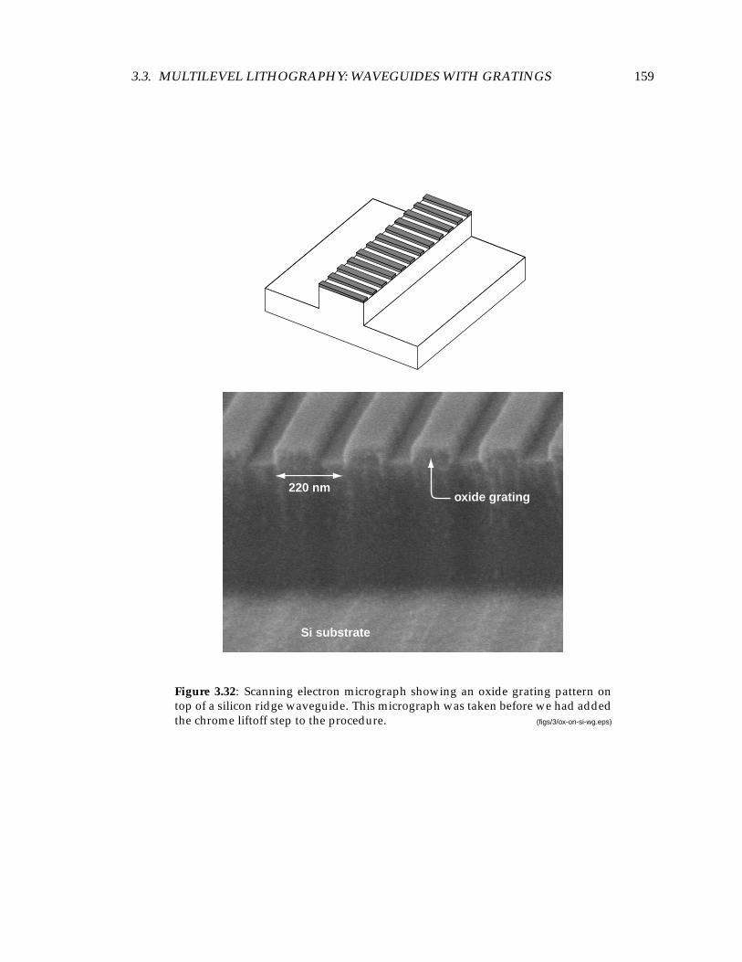
3.3. MULTILEVEL LITHOGRAPHY: WAVEGUIDES WITH GRATINGS 159
Si substrate
oxide grating220 nm
Figure 3.32: Scanning electron micrograph showing an oxide grating pattern ontop of a silicon ridge waveguide. This micrograph was taken before we had addedthe chrome liftoff step to the procedure. (figs/3/ox-on-si-wg.eps)

160 CHAPTER 3. FABRICATION
oxide
silicon
220 nm
Figure 3.33: Deep grating etched into silicon using chlorine reactive-ion etchingwith an oxide mask. Although there is some rounding of the oxide features, themask remains mostly intact. (figs/3/deep-grating-in-si.eps)
mT and a power of 75 W. Figure 3.33 shows the profile of a deep grating etched with theseparameters, illustrating the excellent selectivity to SiO2. 4
Finally, the oxide grating mask is removed using reactive-ion etching in CHF3. Thesample is once again cleaned in an oxygen plasma, and lastly the protective chrome layeris removed in a wet chemical etch. Figure 3.34 shows a completed structure with gratingspatterned on top of the waveguides.
4This high selectivity can often lead to “grass” formation in the large exposed areas in between waveguides.The grass is formed by small amounts of SiO2 which are sputtered away from the mask and redeposited inthe open areas. The protective chrome layer described earlier prevents this grass from forming.

3.3. MULTILEVEL LITHOGRAPHY: WAVEGUIDES WITH GRATINGS 161
4 µm
Figure 3.34: Scanning electron micrograph of a silicon ridge waveguide with inte-grated Bragg grating. (figs/3/si-ridge-with-gr.eps)

162 CHAPTER 3. FABRICATION
3.4 Summary
In this chapter, we described the fabrication techniques for building integrated wave-guides and Bragg gratings. Although we have specifically concentrated on two types ofwaveguides, doped-glass channel waveguides and silicon-on-insulator ridge waveguides,the processes describe here can be easily adapted to other systems.
The fabrication of integrated Bragg gratings involves two lithographic steps: one whichdefines the relatively coarse waveguides features, and one which defines the fine-periodgratings features. This chapter began by describing the techniques for forming waveguidesand couplers. While the waveguides can be patterned using conventional optical pho-tolithography, high-resolution nanolithography must be used to print the Bragg gratings.Therefore, we next described several high-resolution lithographic techniques which aresuitable for patterning Bragg gratings. Finally, we addressed the problem of combiningthese two lithographic techniques to form gratings over waveguides.

Chapter 4
Measurement
Thus far, we have described how to design and construct integrated waveguides, couplersand Bragg gratings. In this chapter we discuss the measurement of the devices we havebuilt. The goal of this segment is to (1) provide a practical description of the measurementtechniques used and (2) present the results of our work. First, we will focus on integratedglass waveguides and couplers, describing the results of our work on an improved direc-tional coupler which has a power-splitting ratio that is insensitive to wavelength, polariza-tion, and fabrication parameters. Next, we will describe our measurements of integratedBragg gratings on silicon-on-insulator ridge waveguides.
4.1 Glass Waveguide Measurements
As mentioned in Section 3.3.3, we have not yet perfected the deposition of glass claddingover fine-period Bragg gratings. Nevertheless, glass waveguides provide an ideal platformfor investigating directional couplers. We describe here the measurement techniques andperformance of a set of directional couplers made with doped-glass waveguides.
4.1.1 Summary of Device Design
We designed and fabricated a set of directional couplers, using the analytical and litho-graphic techniques described earlier. Figure 4.1 depicts schematically the structure of thedirectional couplers, with all of the relevant dimensions labeled.
163

164 CHAPTER 4. MEASUREMENT
θ < 3ο
R = 35 mm
15-17 mm
10.5 µm250 µm
6.6 µm
6.6 µm
10.5 µm
SiO2
Si (substrate)
Ge:SiO2
(a)
(b)
Figure 4.1: (a) Top-down diagram (not to scale) of an integrated directional cou-pler, with all of the dimensions labeled. (b) Cross-sectional view of the wave-guides at the point of minimum separation. The couplers were fabricated in in-tegrated germanium-doped glass channel waveguides, with a nominal refractiveindex contrast of 0.3%. (figs/4/coupler-geometry.eps)

4.1. GLASS WAVEGUIDE MEASUREMENTS 165
The coupler is comprised to two identical square-cross-section channel waveguides,with a nominal width and height of 6.6 µm. These dimensions were chosen to yield singlemode operation and efficient coupling to a standard optical fiber. The materials used wereGe-doped SiO2 waveguides with an index contrast of 0.3%, as specified by the supplier.Based upon the calculated mode profile of this waveguide and that of a standard opticalfiber, we estimate that the transition loss due to mode mismatch at the fiber-waveguideinterface should be less than 0.15 dB.
The radius of curvature was chosen to the 35 mm for all of the devices constructed,and maximum bend angle was approximately 3 degrees. The bending loss for these wave-guides was modeled using a conformal transformation method described elsewhere [83,39]. This bending radius is predicted to yield negligible loss (< 0.5 dB) for the structuresconsidered. Other researchers who have worked with similar waveguides report usingsimilar or slightly larger bending radii [30, 96].
The minimum waveguide separation (center-to-center) was fixed at 10.5 µm, whichleads to an inner-wall separation of 3.9 µm. The on-chip and off-chip waveguide separa-tion was designed to be 250 µm, which allows us to potentially couple light into or out ofboth waveguides with commercially available fiber v-groove arrays.
In addition to conventional directional couplers, we also fabricated a set of improvedinsensitive couplers, using the design rules described in Section 2.2.5. Figure 4.2 illustratesthe structure of the insensitive directional coupler. The relevant device dimensions are thesame as those specified in Fig. 4.1. The target power splitting ratio for these devices was50%, although the design could easily be modified to accommodate any desired power-splitting ratio. The phase delay was achieved by making the upper arm of the deviceslightly longer than the lower arm. The path length difference between the two arms wasapproximately 350-360 nm. We did not include a range of coupling lengths (φ1 and φ2)in our design, rather we simply used our best estimate for these parameters based uponcoupled-mode calculations. We did, however, include a range of phase shifts (θ) aboveand below the nominal design.
4.1.2 Measurement Technique
After the devices were fabricated and over-cladded, the samples were cut into small chipsusing a die saw. The facets were then polished using a Bueler Ecomet tabletop polishingsystem. Initially, we polished with a minimum grit-size of 0.1 µm, but we later found thatgenerally a 0.3 µm grit pad provides a sufficiently smooth surface. The input facets were

166 CHAPTER 4. MEASUREMENT
φ2
φ1
2θ
φi = µLi , 2θ = β∆L
Figure 4.2: Schematic diagram of an improved directional coupler, formed by cas-cading two conventional couplers in a Mach-Zehnder configuration, with an in-tervening phase shift. The three parameters φ1, φ2 and θ were chosen to yielda coupler with 50% splitting ratio, as described in Section 2.2.5. Specifically, wechose φ1 = π/2, φ2 = π/4, and θ = π/3. (figs/4/insensitive-coupler-diagram.eps)
polished normal to the waveguide direction to enable coupling to a cleaved optical fiber,and the output facets were polished at an angle of 10 degrees from the vertical to eliminateunwanted reflections into the waveguide. This polishing scheme causes the light to emergefrom the facet at a small downward angle (out of the plane of the chip).
Figure 4.3 illustrates the setup of our measurement system for characterizing direc-tional couplers. We measured the performance of the couplers using an external cavitytunable diode laser. The attainable wavelength range for the source is approximately 1480–1590 nm.
Light from the laser is first directed through a polarization controller, which allows usto polarize the output light in any desired direction. (The method of polarization controlwill be described later.) Next, a fused-fiber coupler is used to tap off a fraction of the inputlight. This tapped-off signal provides a monitor power against which other measurementsare compared. This allows one to eliminate the effects of drift in the output laser power.
The light is butt-coupled into the waveguide directly from the cleaved facet of the op-tical fiber, using an index-matching gel to suppress reflections at the facet. If the index-matching gel is not used, there is generally a small air gap between the input fiber and thepolished waveguide facet which leads to undesirable Fabry-Perot effects. Even though thefree spectral range of such a thin air gap is typically very large, the measured power willchange substantially if the air gap increases or decreases by a fraction of the optical wave-length. When using an index-matching gel, the input coupling efficiency is insensitive to

4.1. GLASS WAVEGUIDE MEASUREMENTS 167
TunableLaser
MonitorPower
DetectorPolarizationController
10/90
IrisLens
Detector
Iris
Polarizer(optional)
Microscopeobjective
InputFiber
Optical Chip
Normal-polishedFacet
Index-matchingGel (at junction)
Angle-polishedFacet (10o)
(a)
(b)
Figure 4.3: Measurement system used for characterizing integrated couplers. (a)Light from a tunable external cavity diode laser is passed through a polarizationcontroller, 10/90 splitter, and then launched into the device. (b) Light is coupleddirectly from the fiber into the waveguide facet, using an index matching gel. Thesignal emerging from the output facet is imaged onto a photodetector (through alinear polarizer.) (figs/4/coupler-measurement-diagram.eps)

168 CHAPTER 4. MEASUREMENT
the size of the gap between the waveguide and fiber.
At the output facet, the light emerges from the chip into free space, where it is capturedby a microscope objective which forms an image of the chip facet on a detector. An iris isused to selectively measured the light emerging from one waveguide.
The input fiber and a microscope objective are both mounted on 3-axis translationstages, allowing accurate, stable alignment of the input fiber and imaging optics. Theoptical chip is likewise mounted on a translation stage, but this stage is typically keptstationary except when moving from one device to the next.
Initially, the detector is replaced with an infrared camera in order to align the inputfiber and focus the microscope objective on the facet. After the system is aligned, theinfrared camera is replaced with a detector, and each of the alignment stages is adjusted tomaximize the detected power.
As shown in Fig. 4.3b, a linear polarizer is inserted immediately before the iris in orderto determine the polarization state of the light emerging from the waveguide. The inputfiber used in this experiment is not polarization-maintaining, which means that using thepolarization controller alone we cannot accurately predict the polarization state of the lightentering the waveguide. However, by placing a linear polarizer before the detector, it ispossible to fix the polarization state using an empirical approach. First, the linear polarizeris oriented in the vertical (TM) direction. Then, the polarization controller is adjusted tominimize the detected power. This guarantees that the light emerging from the waveguideis TE-polarized 1. Wherever possible, the fiber path between the polarization controllerand the input waveguide is clamped to the table to prevent any twisting or bending whichmight alter the polarization state. After the polarization is adjusted in this manner, thelinear polarizer can be removed (or rotated by 90 degrees). Provided the input fibers arerelatively stationary, this technique provides fairly stable polarization control.
There is unfortunately no easy way to insert a linear polarizer between the input opticalfiber and the chip. We therefore make the assumption that when the light emerging fromthe output facet is TE-polarized, the input light is likewise TE-polarized, and similarly forTM. This assumption is quite reasonable for most integrated waveguides. (In fact, if onecould build an integrated device which rotates the polarization state from TE to TM, itmight solve many of the problems which currently plague integrated optical devices.)
1It is easier in practice to zero the detected power with polarizer in the TM position that it is to maximizethe power with the polarizer in the TE position.

4.1. GLASS WAVEGUIDE MEASUREMENTS 169
The directional couplers are measured by scanning the input laser wavelength whilemeasuring the output power. More specifically, we measure the ratio of the output powerto the monitor power in order to account for any drift or variation in the laser power. Themicroscope objective is then translated in order to image the second output port on thedetector, and wavelength scan is repeated.
4.1.3 Measurement Results
Before measuring the devices, the output of the optical fiber was focused directly onto thedetector in order to quantify the power entering the device. When the device was insertedinto the light path, the total power transmission decreases by approximately 1.5 dB. Thistotal insertion loss figure includes fiber-coupling loss at the input facet, bending loss, andintrinsic waveguide loss.
Figure 4.4a shows the measured splitting ratio for our initial set of directional couplers.These devices were designed to have a power-splitting ratio of 50% at λ = 1550 nm. Asshown, the coupler achieves a splitting ratio which is higher than the desired value of50% for all wavelengths measured and for both polarization states. We attribute this touncertainty in the indices of refraction used in our calculations when designing devices,and structural and material deviations from the nominal design, which may occur dur-ing the various fabrication steps. In principle, this bias can be removed by performing amore exhaustive empirical investigation of the material properties and by more carefullycontrolling and characterizing each step of the fabrication process. However, in additionto this offset, the splitting ratio for the conventional coupler exhibits a sloped wavelengthdependence which is characteristic of directional couplers and cannot be flattened withoutusing a different design.
More importantly, the conventional coupler also exhibits significant polarization de-pendence: the splitting ratio is consistently about 5% higher for TM- than for TE-polarizedlight at all of the wavelengths we measured. This discrepancy cannot be accounted forunless we assume that the index profile of the waveguide is different for TE and TM po-larizations. This can occur if there is birefringence in the deposited glass films, especiallythe top cladding layer which fills the region between the waveguide.
Figure 4.4b plots the measured power-splitting ratio for an improved directional cou-pler, designed using the techniques described in Section 2.2.5. In spite of the polarizationdependence and the apparent uncertainty in material and fabrication parameters, the im-proved coupler achieves a splitting ratio between 45 and 50% (within 5% of the targeted

170 CHAPTER 4. MEASUREMENT
1480
1500
1520
1540
1560
1580
1490
1510
1530
1550
1570
1590
1480
1500
1520
1540
1560
1580
1490
1510
1530
1550
1570
1590
35
40
45
50
55
60
65
70
75
35
40
45
50
55
60
65
70
75
Wavelength (nm)
Sp
litti
ng
Rat
io (
%)
Sp
litti
ng
Rat
io (
%)
TMTE
TMTE
(a) Conventional Directional Coupler
(b) Insensitive Coupler
Figure 4.4: (a) Measured splitting ratio for the initial set of integrated directionalcouplers. The achieved power splitting ratio is uniformly higher than the targetvalue of 50%, for both polarization states. (b) The improved directional couplerexhibits a wavelength-flattened response which is much closer to the desired split-ting ratio. (figs/4/coupler-comparison-orig.eps)

4.1. GLASS WAVEGUIDE MEASUREMENTS 171
value) over the entire wavelength range from 1475 to 1595 nm, with very little polarizationdependence.
We fabricated approximately 12 such cascaded Mach-Zehnder devices, all of them withidentical couplers but with different phase shifts. In principle, it should be possible to pre-cisely control the phase shift (ie, θ) through the photolithographic process. One of themost prevalent integrated optical devices available today, the waveguide-grating-router[141], relies for its operation on a path-length difference which must be lithographicallydefined to the sub-wavelength level. In order to fabricate such a lithographically-definedphase difference in the opposing arms of a Mach-Zehnder interferometer, one must: (1)accurately know the effective index of propagation for the waveguide, and (2) use a pho-tomask that is generated using a grid size that is sufficiently small to properly describe thewaveguides.
In order to help reduce the cost of the photomask set, and to minimize the number ofelectron-beam field boundaries spanned by the device, we used a relatively large grid sizeof 1/8 µm for these initial devices. Moreover, when designing the photomask set, we hadperformed no prior experimental measurements of the effective index for the waveguides.Thus, we simply relied on our best estimate for the effective index, based upon vendor-supplied data. We included a range of phase shifts in the design in order to allow for theuncertainties.
Unfortunately, our measurements indicate that the range of phase shifts (θ) which weactually obtained with these devices was significantly lower than the target value of π/3.Only one of the 12 devices was relatively close to π/3. The data plotted in Fig. 4.4b wasobtained from this device.
In order to address this problem, we fabricated a second set of couplers using ourown e-beam lithography to directly write the patterns. For these devices, the grid sizewas approximately 24 nm, which allows us to more accurately describe the pathlengthdifference. Furthermore, we adjusted the directional couplers in an effort to center thesplitting ratio at the desired value of 50%.
Figure 4.5 presents the measured splitting ratio for the second set of devices. As shownin Fig. 4.5a, the power splitting ratio for the conventional directional coupler is now cen-tered on 50%, but, as expected, the sloped wavelength dependence has not been removed,nor has the polarization-dependence been eliminated. Figure 4.5b presents the measuredpower-splitting ratio for the insensitive directional couplers. As before, the insensitivecouplers achieve a power-splitting ratio that is close to the desired value of 50% for both

172 CHAPTER 4. MEASUREMENT
30
40
50
60
70
30
Wavelength (nm)
Sp
litti
ng
Rat
io (
%)
Sp
litti
ng
Rat
io (
%)
1480
1490
1500
1510
1520
1530
1540
1550
1560
1570
1580
1590
1480
1490
1500
1510
1520
1530
1540
1550
1560
1570
1580
1590
40
50
60
70
TMTE
TMTE
(a) Conventional Directional Coupler
(b) Insensitive Coupler
Figure 4.5: (a) Measured splitting ratio for the second set of integrated directionalcouplers. The achieved power splitting ratio is now centered on 50%, but thereis still a significant polarization-dependence as well as the characteristic slopedwavelength dependence. (b) The measured splitting ratio for the improved direc-tional coupler exhibits a wavelength-flattened response that is much closer to thedesired splitting ratio of 50% (figs/4/coupler-comparison-data.eps)

4.1. GLASS WAVEGUIDE MEASUREMENTS 173
polarization states.
Unfortunately, although the insensitive coupler provides a reduced wavelength-de-pendence, the achieved power-splitting ratio seems to be slightly higher than the desiredvalue of 50%. Recall that the analysis presented in Fig. 2.18 predicts that the insensitivedirectional coupler should be able to correct for relatively large fractional changes whichproportionately affect each of the constituent directional couplers. The reason for the ap-parent discrepancy is that the two constituent directional couplers in the device are notcentered at the same wavelength. That is, the two directional couplers which make up thedevice achieve their nominal values for φ1 and φ2 at two different wavelengths. Our mea-surements indicate that the first directional coupler of the structure, which should nom-inally provide full-power transfer, achieves its target value of φ1 = π/2 at λ = 1518 nmfor the TE polarization, whereas the second directional coupler achieves its nominal valueof φ2 = π/4 at λ = 1547 nm. Because of this, the power-splitting ratio achieved is not asinsensitive as it would otherwise be. Although the structure can compensate for fractionalchanges in φ1 and φ2, it cannot correct for a miscalibration or design flaw which only af-fects one of the directional couplers and not the other. In spite of this limitation, the devicedoes provide improved performance over the conventional directional coupler. Moreover,we believe that this problem can be solved by performing more exhaustive experimentalmeasurements of the waveguide coupling rate.
For the second set of devices, we also investigated the effect of changing the interveningphase shift θ above and below the nominal value of π/3. Figure 4.6 presents the measuredpower-splitting ratio for the insensitive couplers when the phase shift θ is changed by±2and ±4. These plots demonstrate that the device performance is relatively insensitiveto the phase shift θ.
Finally, we looked at how the device response changes when the waveguide widthis increased or decreased with respect to its nominal value. We intentionally fabricatedcouplers which were identical to those described earlier, but with the waveguides madeuniformly wider or narrower in order to simulate the effect of an unintended feature sizebias in the fabrication process. Note that the center-to-center waveguide separations wereheld constant while the waveguide width was changed. Figure 4.7 plots the achievedpower-splitting ratio for the conventional and improved directional couplers when thewaveguide width is increased and decreased by 0.2 µm. As shown in Fig. 4.7b, the insensi-tive directional couplers retain their wavelength-flattened response when the waveguidewidth is changed. There is, however, a small change in the power-splitting ratio as a resultof the change in waveguide width. Again, this change can be ascribed to the miscalibrationof the constituent directional couplers described earlier.

174 CHAPTER 4. MEASUREMENT
30
40
50
60
70
30
40
50
60
70
30
40
50
60
70
30
1480
1490
1500
1510
1520
1530
1540
1550
1560
1570
1580
1590
1480
1490
1500
1510
1520
1530
1540
1550
1560
1570
1580
1590
1480
1490
1500
1510
1520
1530
1540
1550
1560
1570
1580
1590
1480
1490
1500
1510
1520
1530
1540
1550
1560
1570
1580
1590
40
50
60
70
θ = θ0 + 4o
θ = θ0 – 2o θ = θ0 – 4o
θ = θ0 + 2o
TMTE
TMTE
TMTE
TMTE
Sp
litti
ng
Rat
io (
%)
Sp
litti
ng
Rat
io (
%)
Wavelength (nm) Wavelength (nm)
Figure 4.6: Measured performance of the insensitive directional coupler, when theintervening phase shift θ is increased or decreased with respect to its nominal valueof π/3. (figs/4/coupler-vary-theta.eps)

4.1. GLASS WAVEGUIDE MEASUREMENTS 175
30
1480
1490
1500
1510
1520
1530
1540
1550
1560
1570
1580
1590
1480
1490
1500
1510
1520
1530
1540
1550
1560
1570
1580
1590
35
40
45
50
55
60
65
70
30
35
40
45
50
55
60
65
70
Wavelength (nm)
Sp
litti
ng
Rat
io (
%)
Sp
litti
ng
Rat
io (
%)
w = w0w = w0 + 0.2 µmw = w0 – 0.2 µm
w = w0w = w0 + 0.2 µmw = w0 – 0.2 µm
(a) Conventional coupler
(b) Insensitive coupler
Figure 4.7: Measured performance of the insensitive coupler, when the waveguidewidth is biased above and below its nominal value of 6.6 µm. (figs/4/wider-narrower.eps)

176 CHAPTER 4. MEASUREMENT
4.2 Silicon-on-Insulator Waveguide Measurements
4.2.1 Loss Characterization
Before fabricating integrated Bragg gratings, we first constructed a set of conventionalwaveguides in order to evaluate the propagation loss for the structure. In order for aBragg grating to function as desired, the linear loss coefficient (denoted by α) must besignificantly smaller than the grating strength κ. In other words, the rate of reflectioninto the counter-propagating mode must be greater than attenuation rate in order to buildworking Bragg grating devices. Moreover, the propagation loss is an important figure-of-merit for any integrated waveguide. In order to characterize the loss, we fabricated a setof simple straight ridge waveguides of approximately 5 mm length using the techniquesdescribed in Section 3.1.4.
The samples were cut with a die saw and polished using the technique described earlierfor glass waveguides. However, because of the smaller mode size, and higher refractiveindex relative to glass, the samples were polished with a minimum grit-size of 0.05 µm.Prior to dicing, a thick photoresist layer was spun over the waveguides to protect themfrom damage during subsequent sawing and polishing. Both chip facets were polishednormal to the waveguide to facilitate loss measurement via a Fabry-Perot technique[142],which we describe next.
When the chip facets are polished normal to the waveguides, the waveguide forms aFabry-Perot cavity, because of the internal reflection at the air-silicon interface. By measur-ing the spectral response of this cavity, it is possible to infer the waveguide propagationloss. The spectral transmission of a Fabry Perot cavity can be calculated using transfermatrices as described in Section 2.4 [76]. We shall omit the derivation and simply providethe result:
T (β) =T0∣∣∣1− r1r2e−2(α+jβ)L
∣∣∣2 , (4.1)
where T0 is a constant which represents what the power transmission would be in theabsence of any internal reflections, r1 and r2 are the internal amplitude reflectivities at thetwo opposing chip facets, L is the facet-to-facet waveguide length, β is the propagationconstant, and α is the amplitude loss coefficient. This function can be rewritten in the

4.2. SILICON-ON-INSULATOR WAVEGUIDE MEASUREMENTS 177
T0
Tmax
Tmin
T(β)
β
πL
Figure 4.8: Diagram of theoretical Fabry-Perot transmission spectrum, calculatedfor the case where A = |r1r2| exp(−2αL) = 0.2. (figs/4/fabry-calculated.eps)
following simple form:
T (β) =T0
|1−A exp(−2jβL + φ)|2 , (4.2)
where A is a scalar constant, less than 1, which is related to the facet reflectivities and losscoefficient by,
A ≡ |r1r2|e−2αL , (4.3)
and φ is a phase constant which allows for the possible nonzero phase of the complexamplitude reflection coefficients ri. Figure 4.8 plots the calculated power transmission forthe case where A = 0.2.
178 CHAPTER 4. MEASUREMENT
From Eq. 4.2, the ratio of the maximum to the minimum transmission is:
Tmax
Tmin=(1 +A1−A)2
. (4.4)
This equation can be readily inverted to obtain an expression for A in terms of the maxi-mum and minimum transmission.
A =√Tmax −
√Tmin√
Tmax +√Tmin
. (4.5)
Thus, Amay be viewed as a measure of the contrast in the Fabry-Perot spectrum.
The internal reflection coefficient at the chip facet can be approximated using the stan-dard Fresnel reflection equation for normal incidence:
|r| = n− 1n+ 1
. (4.6)
For the waveguides discussed here, because the mode is almost entirely confined in thesilicon core region, one can use n = nSi 3.5 in the above equation.
After measuring the contrast in the Fabry-Perot fringes and inferring the internal reflec-tion from Eq. 4.6, it is possible to estimate the propagation loss using Eq. 4.3 and Eq. 4.5.
Figure 4.9 illustrates the experimental set up used to perform the Fabry-Perot loss mea-surement. As for the glass waveguide measurements described in Section 4.1, the illu-minating source was a tunable external cavity diode laser connected through a polariza-tion controller and 10/90 power splitter. Light was coupled into the waveguides using aconical-shaped lensed fiber, which has a minimum spot size of approximately 5 µm and afocal length of approximately 15 µm. Light emerging from the waveguides was focusedonto a detector through a linear polarizer. Figure 4.10 depicts a representative measuredspectrum for one of the devices considered. Using the equations given above, the propa-gation loss for the sample is calculated to be about 4 dB/cm.
One of the limitations of this technique is that the loss estimate relies upon an accurateestimate of the internal reflectivity at the two facets. For perfect facets, this reflectivityshould be reasonably described by Eq. 4.6. However, if the facet is scratched, damaged,or misoriented, the internal reflectivity might deviate significantly from this estimate. Inpractice, we have noticed that there can be significant device-to-device variation in theloss estimate, even for adjacent waveguides on the same chip. In comparison to the buriedthe glass channel waveguides described earlier, the facets of these air-cladded ridge wave-

4.2. SILICON-ON-INSULATOR WAVEGUIDE MEASUREMENTS 179
Detector
Iris
Polarizer
Microscopeobjective
LensedFiber Optical Chip
Normal-polishedFacet
Ridgewaveguides
Normal-polishedFacet
Fabry-Perot Cavity
Figure 4.9: Experimental setup used to perform Fabry-Perot measurements ofridge waveguides. Light is launched into the waveguide facet using a lensed fiber,while the output facet is imaged onto a photodetector with a microscope objective.The illuminating source (not depicted) was a tunable infrared laser. (figs/4/loss-
measurement-diagram.eps)

180 CHAPTER 4. MEASUREMENT
1550 1550.2 1550.4 1550.6wavelength (nm)
relative frequency (GHz)
Tran
smis
sio
n (
µW
)
1550.8 1551
20
10
0
30
40
50
125 100 75 50 25 0
Figure 4.10: A representative Fabry-Perot transmission spectrum for an integratedsilicon-on-insulator ridge waveguide. The total waveguide length for the samplewas 4.88 mm. The propagation loss inferred from these measurements is approxi-mately 4 dB/cm. (figs/4/fabryloss.eps)

4.2. SILICON-ON-INSULATOR WAVEGUIDE MEASUREMENTS 181
guides are more susceptible to damage during the process of polishing because the guidinglayer is not as well protected. This uncertainty limits the accuracy with which we can es-timate the propagation loss. We point out that this uncertainty would also apply for moreconventional cutback loss measurement techniques.
Based upon our measurements, we estimate a propagation loss of approximately 4± 2dB/cm. This corresponds to an amplitude loss coefficient 2 of α = 0.5 ± 0.2 cm-1, whichis significantly lower than the anticipated grating strengths κ of 3-4 cm-1. The measuredpropagation loss is approximately equivalent (within the measurement uncertainty) for TEand TM polarizations.
4.2.2 Measurement of Integrated Bragg Gratings
After establishing that the propagation loss for the SOI ridge waveguides was sufficientlylow, we next constructed a set of integrated Bragg gratings. Figure 4.11 summarizes therelevant geometrical parameters for these devices.
The waveguide width was 4 µm, and the silicon ridge layer was 3 µm thick at its center.The ridge was etched to a depth of 800 nm. The Bragg gratings were etched to a depth ofabout 150 nm, with a duty cycle of 45-50%, and a period of approximately 223 nm. Thegrating length for the initial set of devices was approximately 4 mm, and the complete chiplength was 17 mm.
In contrast to the couplers described earlier, these devices must be angle-polished onboth facets in order to avoid forming Fabry-Perot cavities between the grating and facets.Figure 4.12 illustrates three possible ways to prepare the chip facets to eliminate internalreflection. The first approach, depicted in Fig. 4.12a refracts the light out of the plane ofthe chip, which makes measurement of the device difficult3. The second method, depictedin Fig. 4.12b corrects this problem but the devices in the set must be staggered. We choseto use the scheme depicted in Fig. 4.12c, in which the waveguides are bent to an angle ofsix degrees at the edges of the chip. With this approach, the facets can be cut and polishednormally. The bending radius was chosen to be 15 mm, which is predicted to yield anegligible bending loss for the waveguides considered.
Figure 4.13 depicts the measurement set up for the integrated Bragg gratings. Notice
2The amplitude loss coefficient α is related to the loss in dB per unit length by α = ln(10)20
× (dB/length)3We were able to use this technique for the glass channel waveguides because the refraction is significantly
weaker for lower-index glass waveguides.

182 CHAPTER 4. MEASUREMENT
4 mm
R = 15 mm
L = 17 mm
θ = 6o
Si
Si (substrate)
SiO2
4 µm
800 nm
1 µm
3 µm
150 nm
(a)
(b)
Figure 4.11: Geometry of the silicon-on-insulator ridge waveguides with Bragggratings. (a) Top-down diagram illustrating overall device dimensions. (b) Wave-guide and grating cross-section. (figs/4/soi-grating-geometry.eps)

4.2. SILICON-ON-INSULATOR WAVEGUIDE MEASUREMENTS 183
top down
side view
side view
side view
top down
top down
(a)
(b)
(c)
Figure 4.12: When measuring integrated Bragg gratings, it is important to elimi-nate internal reflections at the chip facets. This can be achieved by orienting thefacets at an angle with respect to the waveguides. This figure illustrates three dif-ferent ways of angle-polishing the waveguides facets. We have chosen to adoptthe scheme depicted in (c), in which the waveguides are bent slightly at either endof the chip. (figs/4/angle-polishing-schemes.eps)

184 CHAPTER 4. MEASUREMENT
that the chip must be rotated by 21 degrees in order to account for the refraction at the inputand output facets. Light was coupled into the device using a lensed fiber, and imaged atthe output facets using a microscope objective.
Prior to measuring the devices, the output of the lensed fiber was focused directly ontothe detector in order to quantify the relative amount of light entering the device. Afterthe device was inserted and all of the elements aligned, the detected power decreased by12.3 dB for the TE polarization and 13.6 dB for the TM polarization. These insertion lossfigures include mode mismatch at the input facet, waveguide propagation loss, possiblegrating induced loss, Fresnel reflection loss at both facets, and bending loss. The theoreti-cally calculated Fresnel reflection loss is 2.9 dB for TE and 3.5 dB for TM4. From our priormeasurements of the waveguide propagation loss for similar structures without gratings,the waveguide themselves account for 3-10 dB of loss. Because of this uncertainty in ourestimate of the waveguide propagation loss, it is difficult to quantify the excess loss asso-ciated with the grating. However, as we will describe in Appendix C, we also measured 8mm-long Bragg gratings in addition to the 4 mm gratings described here. The measuredinsertion loss did not increase measurably when the grating was made longer, indicatingthat the Bragg gratings introduce very little additional loss.
Figure 4.14 depicts the measured TE transmission spectrum for a 4 mm-long integratedBragg grating. A similar spectrum is seen for the TM polarization. There are four distinctdips in the transmission spectrum (and there might be more at shorter wavelengths whichour laser could not reach.) The first three dips at 1510, 1525, and 1537 nm are causedby coupling of the forward traveling mode to radiation modes. The final dip at 1543 nmcorresponds to the anticipated coupling from the forward to the backward guided mode.We associated the short-wavelength transmission dips with radiation loss after measuringthe device in reflection using a circulator. Whereas there is no measured reflected signal atthe wavelengths corresponding to the first three transmission dips, we saw a peak in thereflected signal at wavelengths corresponding to the transmission dip at 1543 nm.
The radiation loss on the blue side of the spectrum is a well studied phenomenon forfiber Bragg gratings [143]. As in the case of fiber Bragg gratings, this loss can be identi-fied with grating-assisted coupling between the forward-traveling mode and backward-traveling cladding modes. The spectrum of the cladding modes can be computed usingthe beam propagation method, as described in reference [143].
To illustrate the physical mechanism of this radiation mode coupling, consider the sim-
4Because the waveguide are illuminated at an angle to the facet, the reflection is different for TE and TM,which is why the computed Fresnel reflection loss differs between the two polarization states.

4.2. SILICON-ON-INSULATOR WAVEGUIDE MEASUREMENTS 185
Detector
Iris
Polarizer
Microscopeobjective
(a)
(b)
LensedFiber
Optical Chip
Normal-polished
Facets
Ridgewaveguides
Silicon (n = 3.5)
Air (n = 1.0)
Facet
θ0 = 21.5o
θ1 = 6o
Figure 4.13: (a) Experimental setup used to measure the transmission spectral re-sponse for integrated Bragg gratings in silicon-on-insulator ridge waveguides. (b)Enlarged diagram depicting the light path at the input facet. Because the wave-guides approach the facet at an angle of six degrees from the normal, the entirechip must be rotated by 21 degrees to allow for refraction as the light enters thechip. (figs/4/grating-measurement-diagram.eps)

186 CHAPTER 4. MEASUREMENT
1505 1510 1515 1520 1525 1530 1535 1540 1545-30
-25
-20
-15
-10
-5
0
wavelength (nm)
Tran
smis
sio
n (
dB
)
3rd leaky mode
2nd leaky mode
1st leaky mode
fundamentalmode
Figure 4.14: Measured transmission spectral response for a 4 mm long Bragg grat-ing on a silicon-on-insulator ridge waveguide. The spectral response shows fourdistinct dips in transmission. The three peaks on the blue side of the spectrumare attributed to radiation loss, whereas the narrow dip at 1543 nm corresponds toBragg reflection into the backward-traveling bound mode. (figs/4/radiationmodes.eps)

4.2. SILICON-ON-INSULATOR WAVEGUIDE MEASUREMENTS 187
SiO2
Si n = 3.63 µm
n = 1.46
n = 1air
Figure 4.15: The nature of the radiation losses seen in Fig. 4.14 can be explained byconsidering this simplified structure consisting of a simple SiO2:Si:air slab wave-guide whose dimensions are chosen to be similar to the ridge waveguide whichwe actually measured. (figs/4/simple-slab-model.eps)
plified problem of a silicon slab waveguide, whose dimensions are chosen to be similar tothe ridge waveguide which we actually measured. Specifically, we let the silicon guidinglayer be 3 µm thick and we assume that the lower cladding is SiO2 (n = 1.46) and the up-per cladding is air (n = 1), as depicted in Fig. 4.15. The propagation constants, βi, can becomputed exactly for each of the modes of this structure[14]. Figure 4.16 depicts the calcu-lated dispersion relation (β vs. λ) for the first four TE modes of the structure. Notice thatwe have also plotted the negative propagation constants which correspond to the lowestfour backward-travelling modes. The Bragg grating creates a coupling between the modeswherever the difference in propagation constants is equal to the k-vector of the grating:
βn(λ)− βm(λ) = 2πΛ
. (4.7)
The four arrows drawn in Fig. 4.16 illustrate the four wavelengths at which light from theforward-traveling fundamental mode can couple to a backward traveling mode. The posi-tion and relative spacing of these four wavelengths agrees qualitatively with the measureddata presented in Fig. 4.14, in spite of the simplified approximations made (i.e., replacingthe ridge with a slab.)
Of course, the ridge waveguide was designed to have only one bound mode (for eachpolarization state), which raises the question of why we measure these extraneous dipsin the transmission. The explanation is that although the waveguide only supports onebound mode, there are several leaky modes associated with the higher-order slab modes ofthe structure. For these leaky modes, the mechanism of power loss is that the light escapes

188 CHAPTER 4. MEASUREMENT
1500
1510
1520
1530
1540
1550
1560
1570
1580
1.3
-1.3
1.4
-1.4
1.5
-1.5
λ (nm)
β (x 105 cm-1)b
ackward
mo
des
forw
ardm
od
es
k g =
Λ2π
1
-1-2
-3
-4
23
4
Figure 4.16: Calculated dispersion relation (β vs. λ) for the first four modes of theslab waveguide structure depicted in Figure 4.15. The corresponding backward-traveling modes (with negative values for β) are also plotted. Coupling can occurbetween modes wherever the difference in propagation constants matches the spa-tial frequency (k-vector) of the Bragg grating. The four vertical lines in this figureindicate the four wavelengths at which light from the forward-traveling funda-mental mode can couple to one of the four backward-traveling modes. (figs/4/leaky-slab-
simulation.eps)

4.3. SUMMARY 189
by leaking out into the silicon slab on either side of the ridge. By contrast, the fundamentalmode is completely confined by the ridge, meaning that the fields decay evanescantly toeither side of the ridge.
Figure 4.17 is an expanded plot of the fundamental Bragg transmission spectrum. Wehave included both TE and TM spectra for comparison. The separation between the TEand TM peaks is approximately 50 GHz, or 0.4 nm. The theoretically predicted modalbirefringence for the structure is 43 GHz, or 0.35 nm. Another effect seen in Fig. 4.17 is thatthe TE-polarized mode experiences a stronger Bragg reflection than the TM mode. Basedupon the depth of the transmission response, we estimate that the grating strength (κ) is4.5 cm-1 for the TE mode and 2.1 cm-1 for the TM mode. The TE grating strength agreeswell with calculations based on coupled mode theory. (cf Fig. 2.23), while the TM result issomewhat lower than the value of 3.7 cm-1 predicted by coupled mode theory.
Figure 4.18 plots a comparison between the measured theoretical spectral response (forTE polarization) and the calculated spectral response, assuming κ = 4.5 cm-1. The inferredpeak reflectivity of this structure is approximately 90%, and bandwidth (at half-maximum)is approximately 15 GHz. Although the reflectivity of this structure is not high enough tocompete with fiber Bragg gratings or other currently used high-performance WDM filters,this represents to our knowledge the first experimental demonstration of an integratedBragg grating in an SOI ridge waveguide.
As discussed in Section 2.3.3, when extracting a modulated data signal from a noisybackground, the optimal filter is not a flat bandpass filter but a matched filter. The lengthof the gratings considered here were chosen to yield a spectral response which is approxi-mately matched to a 10 Gb/s on-off encoded optical signal.
4.3 Summary
We have described in this chapter the measurement and characterization of integratedwaveguides, couplers, and Bragg gratings. Specifically, we investigated a series of direc-tional couplers, fabricated in glass channel waveguides, and we demonstrated an inte-grated Bragg grating filter fabricated on a silicon-on-insulator ridge waveguide.
For the glass waveguide devices, we presented a comparison between conventionalsingle-stage directional couplers and a more sophisticated cascaded coupler. We demon-strated that by connecting two dissimilar directional couplers with an intervening phaseshift, one can obtain a power-splitting ratio that is insensitive to wavelength, polariza-

190 CHAPTER 4. MEASUREMENT
1542.6 1543 1543.4 1543.8 1544.2 1544.6-12
-10
-8
-6
-4
-2
0
wavelength(nm)
relative frequency (GHz)
Tran
smis
sio
n (
dB
)
0 -40 -80 -1204080120
TM
TE
Figure 4.17: Transmission spectrum for the 4 mm-long Bragg grating. For compar-ison, both TE and TM polarizations are plotted. The TM data has been offset by -2dB in order to more clearly differentiate the two spectra. The separation betweenthe TE and TM peaks indicates that the birefringence for the structure is approxi-mately 50 GHz, or 0.4 nm. The estimated grating strength for the TE polarizationapproximately 2× larger than for the TM polarization. (figs/4/tetmcompare4.eps)

4.3. SUMMARY 191
-40 -30 -20 -10 0 10 20 30 40
-10
-8
-6
-4
-2
0
relative frequency(GHz)
Tran
smis
sio
n (
dB
)
TheoryLg = 4 mmκ = 4.5 cm-1
Λ = 223 nm
MeasuredTE polarization
λλ0 = 1545 nm
Figure 4.18: A comparison between the measured spectral response for the 4 mm-long Bragg grating, and that predicted from coupled mode theory. The gratingstrength used in the theoretical model was 4.5 cm-1. (figs/4/grating-spectrum-fit-4.eps)

192 CHAPTER 4. MEASUREMENT
tion, and fabrication parameters. Others have recognized that wavelength insensitivitycan be achieved using such a Mach-Zehnder structure, but their design technique in-volves numerical optimization based upon measured wavelength-dependence data [51].This approach does not explicitly account for polarization dependence or other fabricationuncertainties, and it cannot be easily extended to other waveguide systems. Our mea-surements show, by direct comparison with a similarly fabricated directional coupler, thatwavelength-insensitive and polarization-insensitive performance can be achieved usingthe relatively simple analytical design rules described in Section 2.2.5. The couplers whichwe constructed achieved close to 50 percent power splitting over the entire wavelengthrange from 1475-1590 nm, for both polarization states.
For the silicon-on-insulator devices, we measured and analyzed the spectral responseof a set of integrated Bragg gratings. Our measured spectral response shows reasonableagreement with that predicted by the coupled mode theory described in Section 2.3. Thefilters achieve a bandwidth of 15 GHz, for a 4 mm-long grating, with a peak reflectivityof 90% for the TE polarization and 50% for the TM polarization. Furthermore, we de-scribed a simple model which explains the origin of the radiation loss which we observedon the blue side of the spectrum. To date, most of the integrated filters fabricated in SOIare resonator-based structures, based on sub-micron size silicon channel waveguides[144].The Bragg grating structures demonstrated here operate on a completely different princi-ple. Although it is somewhat misleading to compute a Q (quality factor) for these devices,we can point out that for a resonator-based device to have the same bandwidth as theBragg grating filter described here, would require a Q of 13,000.

Chapter 5
Conclusions
5.1 Summary
This thesis has sought to provide a thorough description of my research in integratedBragg grating filters. The work was grouped into three principal chapters describing, re-spectively, the design, fabrication and measurement of devices. This ordering, while log-ical, doesn’t necessarily describe the actual or even the optimal sequence of events: mostsuccessful device development projects involve many cycles of iteration and prototyping.
The design of integrated optical devices begins with an electromagnetic analysis ofdielectric structures. To this end, I developed and implemented a set of finite differenceroutines which accurately predict the electromagnetic modes of integrated waveguides.These routines are crucial not only in designing such structures, but in understandingtheir observed behavior. Once the electromagnetic modes are well-characterized, the be-havior of more complicated systems consisting of multiple waveguides and gratings canbe simulated using coupled mode theory. In coupled mode theory, Maxwells equations arereplaced by a set of coupled linear differential equations in which the coupling coefficientsare related to overlap integrals involving the electromagnetic modes of the waveguide.I describe how the coupled mode equations can be applied to directional couplers andBragg gratings, including the case where the gratings are apodized or chirped. Finally, thesolution to the coupled differential equations can be expressed in the form of a transfermatrix. Complicated aggregate devices can be easily modeled by simply multiplying theirrespective transfer matrices.
The fabrication of integrated photonic devices presents several unique problems which
193

194 CHAPTER 5. CONCLUSIONS
have not been adequately addressed by the microfabrication community. I implementedspecialized software routines for generating the long, slowly curved waveguide patternsrequired in waveguides and directional couplers. I described a flexible fabrication method-ology for patterning integrated waveguides, couplers, and Bragg gratings in two differ-ent material systems: integrated glass channel waveguides and silicon-on-insulator ridgewaveguides. The relevant lithographic tools used to build these devices include conven-tional optical lithography, scanning-electron-beam lithography, interference lithography,and x-ray nanolithography. The goal of our fabrication efforts has been to bring togetherall of these techniques in an efficient and robust process.
Finally, the measurements of fabricated devices were presented, along with a descrip-tion of the measurement techniques. For the glass waveguide system, I demonstrated animproved directional coupler that shows reduced sensitivity to wavelength and polariza-tion. In the silicon-on-insulator system, I measured and characterized a series of integratedBragg gratings. A simple physical model was presented to explain the anomalous loss intransmission which was observed in the blue side of the spectrum. The measured spectralresponse agrees well with theoretical predictions based upon coupled mode analysis.
5.2 Future Work
No one enjoys writing a document about the things they didn’t do. Nevertheless, inte-grated optics is an exciting research field and like every exciting field there is an endlesssupply of challenging problems to consider. Although my work in this field has allowedme to design, fabricate and measure integrated photonic devices, there is much room forimprovement, and there are many stones which have been left unturned.
The finite difference routines which I described are adequate for many devices, butthere exist more advanced numerical techniques for simulating waveguides. In particular,the routines which I describe have a numerical accuracy (grid quantization error) which isproportional to the grid size ∆x∆y. Most commercially available numerical mode solversuse a similar set of routines with the same accuracy order. The design and analysis of inte-grated photonic structures could benefit significantly from routines which converge morerapidly with decreasing grid size. For example, if the numerical accuracy were propor-tional to ∆x2∆y2, one wouldn’t need to use as fine a grid size to accurately compute themode structure[145, 146]. Another improvement which could be made would be to mod-ify the existing program to implement the beam propagation method. This would enableone to numerically model structures like tapers, bends, and y-branches.

5.2. FUTURE WORK 195
The coupled mode analysis for integrated Bragg gratings seems to accurately predictthe coupling coefficient κ for the TE polarization, but overestimates the coupling coefficientfor the TM polarization. This discrepancy might be caused by the fact that we neglectedthe longitudinal field component ez when computing the grating strength overlap integral.More attention should be devoted to the problem of calculating the coupling coefficientκ, especially for high index contrast systems where there can be significant polarizationdependence.
Interference lithography is an extremely powerful tool for building integrated Bragggratings, but more work is needed to characterize and eliminate the phase distortion pro-duced by these interference lithography systems. In particular, because the systems cur-rently used in the NanoStructuresLab employ spherical waves, the gratings produced havean inherent chirp which limits the usable grating length in practical applications. In orderto construct longer Bragg grating filters, it will be necessary to either use some other litho-graphic means, or renovate the interference lithography systems to eliminate this chirp.
For the glass waveguide devices, we have not yet solved the problem of maintain-ing the grating structure during the cladding overgrowth process. One potential solutionwould be to etch the grating into the lower cladding layer before depositing the core. Sincethe bottom SiO2 base layer should have the highest glass transition temperature in the sys-tem, presumably this approach would not suffer from the same problems of reflow. Asthe integrated optics community becomes more interested in smaller, high-index-contrastwaveguides, the problem of maintaining the structural fidelity of the structure duringovergrowth will become even more important.
The silicon-on-insulator devices could be improved in several ways. First, we have notbeen careful in our initial experiments to minimize the birefringence of the devices. Moreexperimental and theoretical investigation of these devices could lead to a design whichhas little or no birefringence. Another significant limitation of this material systems is thepolarization-dependence in the grating strength κ. One potential solution to this problemwould be to corrugate the sidewalls of the structure in addition to the top surface, in orderto balance the TE and TM feedback. The devices which we measured had a mode sizewhich was slightly too small to allow efficient butt-coupling to an optical fiber. While thestructure could be made larger without sacrificing single-mode operation, it becomes hardto achieve a sufficiently high grating strength κ for a large waveguide. Again, there mightbe a way to improve the grating strength by corrugating the sidewalls and the other siliconregions outside of the ridge.
The coupling to leaky modes on the blue side of the spectrum is another effect which

196 CHAPTER 5. CONCLUSIONS
deserves further investigation. Although radiation loss is an undesirable effect for add/drop filters, it might be possible to exploit this effect for other applications such as gainequalization.
Having demonstrated integrated directional couplers and integrated Bragg gratingsseparately, the next task will be to assemble these two building blocks into an integratedMach-Zehnder interferometer, in order to separate the reflected signal from the input sig-nal. The ability to integrate directional couplers and gratings in this way without the needfor any post-fabrication trimming or adjustment could prove to be the strongest sellingpoint for integrated Bragg gratings filters.
Finally, much can be done to optimize the spectral response of a Bragg grating by in-tentionally introducing chirp and apodization. The theoretical framework presented inthis thesis describes how to analyze and design such a structure, but the devices whichwe have built to date have not taken advantage of these degrees of freedom. One wayto achieve apodization is to adjust the lateral extent of the grating, by making the gratingonly cover part of the waveguide rather than the entire waveguide. Another way wouldbe to adjust the depth of the grating across the device. For Bragg gratings formed by phys-ical corrugations, the process of apodization invariably changes the effective index of thewaveguide. For this reason, apodization and chirp are inextricably tied together. There aretwo ways to construct a filter with pure apodization. One way is to modify the waveguidewidth in tandem with the apodization profile such that the effective index of the wave-guide remains constant. Another approach would be to intentionally chirp the grating inaddition to apodization in order to compensate for the change in effective index inducedby the apodization.
I have mentioned here a few of the possible directions for future research, but the pos-sible applications of integrated Bragg gratings are limited only by the imagination. It ismy hope that this work provides enough theoretical and experimental information to en-courage others to develop new creative ideas and applications.

Appendix A
Finite Difference Modesolver
Section 2.1.4 introduced the topic of finite difference methods by describing an approxi-mate solution method for the scalar eigenvalue equation. The scalar eigenvalue equationis valid whenever the index contrast of the waveguide is small. The derivation presentedin Section 2.1.4 assumes that the scalar field and its derivative are continuous at all pointsand the transverse planes. However, Maxwells equations clearly state that some of thetransverse field components are discontinuous across abrupt dielectric interfaces. This ap-pendix details how the finite difference equations can be modified to account for thesepredictable discontinuities in the electromagnetic fields. The reader should refer to Section2.1.4, which defines the geometry of the finite difference mesh and introduces the notationused to label grid points.
A.1 Vector Finite Difference Method
First, consider the differential operator Pxx which operates on ex in the full-vector eigen-mode equation (Eq. 2.25):
Pxxex =∂
∂x
[1n2
∂(n2ex)∂x
]+∂2ex∂y2
+ n2k2ex . (A.1)
Now suppose that we wish to approximate this differential operator with a finite differencescheme. As before, we shall use the subscripts P , N , S, E andW to label the point underconsideration and its closest neighbors to the north, south, east and west respectively. If therefractive index is the same for all five of these points, we may simply use the scalar finite
197

198 APPENDIX A. FINITE DIFFERENCE MODESOLVER
difference scheme described in Eq. 2.45. Also, because ex is continuous across horizontalinterfaces, the ∂2ex
∂y2 term may be approximated with the simple three point difference ofEq. 2.42. However, when there is an index discontinuity betweenW and P or between Pand E, the finite difference equations must be modified to account for the discontinuityin ex. To accomplish this, we use a modified interpolation procedure in which we fit thepoints exW , exP and exE with a piecewise quadratic polynomial.
φ(x) =
AW +Bx+ Cx2 in cell W
AP +Bx+ Cx2 in cell P
AE +Bx+ Cx2 in cell E
(A.2)
The interpolating function φ(x) is identical to Eq. 2.37 except that it allows for a possiblediscontinuity at the edge of each cell. We have further assumed that the first and secondderivatives (or equivalently the polynomial coefficients B and C) are continuous acrosscell boundaries.
As before, we require that the interpolating function passes through the three pointsexW , exP and exE :
exW = AW −B∆x+ C(∆x)2exP = APexE = AE +B∆x+C(∆x)2
(A.3)
But we now add additional constraints that describe the continuity of n2ex at x = ±∆x2 :
n2W
AW − 1
2B∆x+
14C(∆x)2
= n2
P
AP − 1
2B∆x+
14C(∆x)2
n2P
AP +
12B∆x+
14C(∆x)2
= n2
E
AE +
12B∆x+
14C(∆x)2
(A.4)
Eq. A.3 and Eq. A.4 together give five linear equations which can be solved for the five un-known polynomial coefficients. (Actually, B and C are the only two coefficients of interestbecause they describe respectively the first and second derivatives of ex.) For brevity, we

A.1. VECTOR FINITE DIFFERENCE METHOD 199
shall omit the algebraic steps, and simply summarize the results.
∂φ
∂x= B =
1∆x
−(n2Wn
2P + 3n2
En2W )
n4P + 2n2
En2P + 2n2
Wn2P + 3n2
En2W
exW+
3(n2E − n2
W )n2P
n4P + 2n2
En2P + 2n2
Wn2P + 3n2
En2W
exP +
(n2En
2P + 3n2
En2W )
n4P + 2n2
En2P + 2n2
Wn2P + 3n2
En2W
exE
(A.5)
∂2φ
∂x2= 2C =
1(∆x)2
4(n2
Wn2P + n2
En2W )
n4P + 2n2
En2P + 2n2
Wn2P + 3n2
En2W
exW+
4(n2En
2P + n2
Wn2P + 2n2
En2W )
n4P + 2n2
En2P + 2n2
Wn2P + 3n2
En2W
exP +
4(n2En
2P + n2
En2W )
n4P + 2n2
En2P + 2n2
Wn2P + 3n2
En2W
exE
(A.6)
Eq. 2.42 and Eq. A.6 can be combined to yield the finite difference representation of theoperator Pxx.
Pxx :
01
(∆y)2 0
αW(∆x)2 n2
P k2− 2
(∆y)2− 2αP
(∆x)2αE
(∆x)2
01
(∆y)2 0
(A.7)
Where the constants αW , αP and αE are dimensionless ratios defined by:
αW ≡ 4(n2Wn
2P + n2
En2W )
n4P + 2n2
En2P + 2n2
Wn2P + 3n2
En2W
(A.8)
αP ≡ 2(2n4P + n2
En2P + n2
Wn2P )
n4P + 2n2
En2P + 2n2
Wn2P + 3n2
En2W
(A.9)
αE ≡ 4(n2En
2P + n2
En2W )
n4P + 2n2
En2P + 2n2
Wn2P + 3n2
En2W
(A.10)
A similar analysis applied to ey leads to the following finite difference representation

200 APPENDIX A. FINITE DIFFERENCE MODESOLVER
of Pyy :
Pyy :
0γN
(∆y)2 0
1(∆x)2
n2Pk
2− 2γP(∆y)2
− 2(∆x)2
1(∆x)2
0γS
(∆y)2 0
(A.11)
Where the constants γS and γN are dimensionless ratios defined by:
γS ≡ 4(n2Sn
2P + n2
Nn2S)
n4P + 2n2
Nn2P + 2n2
Sn2P + 3n2
Nn2S
(A.12)
γP ≡ 2(2n4P + n2
Nn2P + n2
Sn2P )
n4P + 2n2
Nn2P + 2n2
Sn2P + 3n2
Nn2S
(A.13)
γN ≡ 4(n2Nn
2P + n2
Nn2S)
n4P + 2n2
Nn2P + 2n2
Sn2P + 3n2
Nn2S
(A.14)
The finite difference approximations for Pxy and Pyx are slightly more complicatedbecause these differential operators involve mixed partial derivatives in both directions.However, the framework described above can be used to compute a mixed partial deriva-tive by simply applying the finite difference approximations for ∂
∂x and ∂∂y separately. We
will illustrate this technique for the simple case where we wish to approximate ∂2f∂x∂y for
a continuous function f(x, y). To approximate ∂2f∂x∂y |P we first use the three point finite
difference approximations to obtain ∂f∂y |W and ∂f
∂y |E ,
∂f
∂y|W 1
2∆y(fNW − fSW ) (A.15)
∂f
∂y|E 1
2∆y(fNE − fSE) (A.16)
(A.17)
Notice that we have now introduced the new subscriptsNW , SW ,NE and SE to label thepoints northwest, southwest, northeast and southeast respectively. Now, we simply applya similar finite difference equation in horizontal direction, giving,
∂2f
∂x∂y|P 1
2∆x
∂f
∂y|E − ∂f
∂y|W
(A.18)
∂2f
∂x∂y|P 1
4∆x∆yfNE − fSE − fNW + fSW (A.19)

A.1. VECTOR FINITE DIFFERENCE METHOD 201
Thus, the finite difference representation of the differential operator ∂2
∂x∂y is
∂2
∂x∂y:
− 14∆x∆y 0 +
14∆x∆y
0 0 0
+1
4∆x∆y 0 − 14∆x∆y
(A.20)
It is easy to to verify that for continuous functions, the finite difference representationof ∂2
∂y∂x is the same as for ∂2
∂x∂y . The discretized operators corresponding to Pyx can bederived by applying a similar analysis with the modified finite-difference model describedin Eq. A.6. This yields the following finite difference representation of Pyx:
Pyx :
1− αNW
4∆x∆y3(αNE − αNW )
4∆x∆yαNE − 14∆x∆y
0 0 0
αSW − 14∆x∆y
3(αSW − αSE)4∆x∆y
1− αSE4∆x∆y
(A.21)
Where the constants αNE , αNW , αSE and αSW , are again dimensionless ratios which be-come 1 in the absence of dielectric interfaces.
αNE ≡ 2(n2NEn
2N + 3n2
NEn2NW )
n4N + 2n2
NEn2N + 2n2
NWn2N + 3n2
NEn2NW
(A.22)
αNW ≡ 2(n2NWn
2N + 3n2
NEn2NW )
n4N + 2n2
NEn2N + 2n2
NWn2N + 3n2
NEn2NW
(A.23)
αSE ≡ 2(n2SEn
2S + 3n2
SEn2SW )
n4S + 2n2
SEn2S + 2n2
SWn2S + 3n2
SEn2SW
(A.24)
αSW ≡ 2(n2SWn
2S + 3n2
SEn2SW )
n4S + 2n2
SEn2S + 2n2
SWn2S + 3n2
SEn2SW
(A.25)
Likewise, the finite difference representation of Pxy is:
Pxy :
1− γNW
4∆x∆y 0γNE − 14∆x∆y
3(γSW − γNW )4∆x∆y
03(γNE − γSE)
4∆x∆yγSW − 14∆x∆y 0
1− γSE4∆x∆y
(A.26)

202 APPENDIX A. FINITE DIFFERENCE MODESOLVER
where the four constants γNE , γNW , γSE and γSW are given by:
γNE ≡ 2(n2NEn
2E + 3n2
NEn2SE)
n4E + 2n2
NEn2E + 2n2
SEn2E + 3n2
NEn2SE
(A.27)
γSE ≡ 2(n2SEn
2E + 3n2
NEn2SE)
n4E + 2n2
NEn2E + 2n2
SEn2E + 3n2
NEn2SE
(A.28)
γNW ≡ 2(n2NWn
2W + 3n2
NWn2SW )
n4W + 2n2
NWn2W + 2n2
SWn2W + 3n2
NWn2SW
(A.29)
γSW ≡ 2(n2SWn
2W + 3n2
NWn2SW )
n4W + 2n2
NWn2W + 2n2
SWn2W + 3n2
NWn2SW
(A.30)
Examination of Eq. A.21 and Eq. A.26 reveals that the matrix elements of the finite dif-ference operators Pxy and Pxy vanish except for points which are located next to dielectricinterfaces. Thus, it is the presence of dielectric interfaces which couples the two transversefield components.
For reference, I have summarized the finite difference implementation of the full-vectoreigenmode problem in Tables A.1 and A.2.
To summarize, we have described a technique for developing finite difference approxi-mations which can be applied even in the presence of abrupt dielectric interfaces where thefield is discontinuous. The technique described here involves fitting a piecewise-quadraticpolynomial to three adjacent grid points. Other authors have developed similar techniquesfor accounting for the field discontinuity. Most notably, Stern [21] describes a techniquefor modeling field discontinuities using only two adjacent grid points. For simple one-dimensional problems which can be solved exactly, I have found that the discretizationpresented here yields a solution which is 3-4× more accurate for the same grid size.
A.2 Finite Difference Boundary Conditions
Thus far, we have concentrated on developing finite difference representations of partialdifferential equations, without regard to the edges of the computation window. The finitedifference approximations given in the previous section can be applied without modifica-tion to all internal points in the computation window. But for points which lie on the edgeof the computation window, boundary conditions must be considered. We will describehere three different boundary conditions: symmetric, antisymmetric, and absorbing.
By “absorbing”, we mean that the field is assumed to be zero at grid points immediately

A.2. FINITE DIFFERENCE BOUNDARY CONDITIONS 203
Pxxe x
≡∂ ∂x
[ 1 n2
∂(n
2e x)
∂x
] +∂
2e y∂y
2+n
2k
2e x
Pxye y
≡∂ ∂x
[ 1 n2
∂n
2e y∂y
] −∂
2e y
∂x∂y
01
(∆y)2
0
αW
(∆x)2
n2 Pk
2−
2(∆y)2−
2αP
(∆x)2
αE
(∆x)2
01
(∆y)2
0
1−γNW
4∆x∆y
0γNE−
14∆x∆y
3(γSW
−γNW)
4∆x∆y
03(γNE−γSE)
4∆x∆y
γSW
−1
4∆x∆y
01−γSE
4∆x∆y
Pyxe x
≡∂ ∂y
[ 1 n2
∂n
2e x∂x
] −∂
2e x
∂y∂x
Pyye y
≡∂
2e y∂x
2+∂ ∂y
[ 1 n2
∂(n
2e y)
∂y
] +n
2k
2e y
1−αNW
4∆x∆y
3(αNE−αNW)
4∆x∆y
αNE−
14∆x∆y
00
0
αSW
−1
4∆x∆y
3(αSW
−αSE)
4∆x∆y
1−αSE
4∆x∆y
0γN
(∆y)2
0
1(∆x)2
n2 Pk
2−
2γP
(∆y)2−
2(∆x)2
1(∆x)2
0γS
(∆y)2
0
Tab
leA
.1:A
sum
mar
yof
full-
vect
orfin
ite
dif
fere
nce
equa
tion
sfo
rth
etr
ansv
erse
efi
eld
s.E
ach
ofth
efin
ite
dif
fere
nce
oper
ator
sis
repr
esen
ted
bya
3by
3ta
ble
whi
chd
escr
ibes
the
finit
ed
iffe
renc
eco
effic
ient
sfo
rth
epo
intu
nder
cons
ider
atio
nan
dth
ene
ighb
orin
gei
ghtp
oint
s.Fo
rex
ampl
e,th
eup
per
left
-han
del
emen
toft
heP
yx
tabl
ere
pres
ents
the
coef
ficie
ntw
hich
mul
tipl
iese x
NW
inth
efin
ite
dif
fere
nce
appr
oxim
atio
nofP
yxe x
.T
heco
nsta
ntsα
νa
ndγ
νa
red
imen
sion
less
rati
os,
tabu
late
din
Tabl
eA
.2.
Eac
hof
thes
eco
nsta
nts
eval
uate
sto
1in
the
abse
nce
ofd
iele
ctri
cin
terf
aces
.

204 APPENDIX A. FINITE DIFFERENCE MODESOLVER
αW
≡4(n
2Wn
2P+n
2En
2W)
n4P+
2n2En
2P+
2n2Wn
2P+
3n2En
2W
γS
≡4(n
2Sn
2P+n
2Nn
2S )n
4P+
2n2Nn
2P+
2n2Sn
2P+3n
2Nn
2S
αP
≡2(2n
4P+n
2En
2P+n
2Wn
2P)
n4P+
2n2En
2P+
2n2Wn
2P+
3n2En
2W
γP
≡2(2n
4P+n
2Nn
2P+n
2Sn
2P)
n4P+
2n2Nn
2P+
2n2Sn
2P+3n
2Nn
2S
αE
≡4(n
2En
2P+n
2En
2W)
n4P+
2n2En
2P+
2n2Wn
2P+
3n2En
2W
γN
≡4(n
2Nn
2P+n
2Nn
2S )n
4P+
2n2Nn
2P+
2n2Sn
2P+3n
2Nn
2S
αNE
≡2(n
2NEn
2N+
3n2NEn
2NW)
n4N+
2n2NEn
2N+
2n2NWn
2N+
3n2NEn
2NW
γNE
≡2(n
2NEn
2E+
3n2NEn
2SE)
n4E+
2n2NEn
2E+2n
2SEn
2E+
3n2NEn
2SE
αNW
≡2(n
2NWn
2N+
3n2NEn
2NW)
n4N+
2n2NEn
2N+
2n2NWn
2N+
3n2NEn
2NW
γNW
≡2(n
2NWn
2W+
3n2NWn
2SW)
n4W
+2n
2NWn
2W+
2n2SWn
2W+
3n2NWn
2SW
αSE
≡2(n
2SEn
2S+
3n2SEn
2SW)
n4S+
2n2SEn
2S+
2n2SWn
2S+
3n2SEn
2SW
γSE
≡2(n
2SEn
2E+
3n2NEn
2SE)
n4E+
2n2NEn
2E+2n
2SEn
2E+
3n2NEn
2SE
αSW
≡2(n
2SWn
2S+
3n2SEn
2SW)
n4S+
2n2SEn
2S+
2n2SWn
2S+
3n2SEn
2SW
γSW
≡2(n
2SWn
2W+
3n2NWn
2SW)
n4W
+2n
2NWn
2W+
2n2SWn
2W+
3n2NWn
2SW
Table
A.2:A
summ
aryofthe
dim
ensionlessconstants
usedin
thefinite
difference
scheme
givenin
TableA
.1.Notice
thateachofthe
constantsd
efinedhere
becomes
1w
henthere
areno
index
discontinuities.
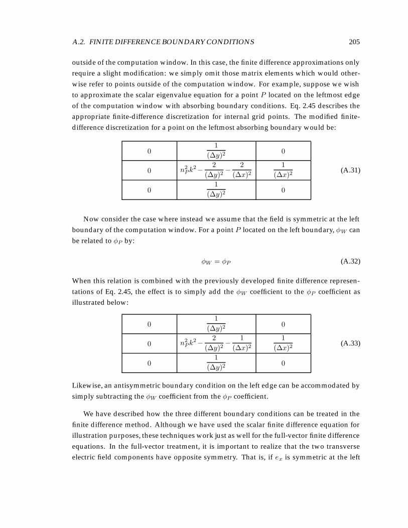
A.2. FINITE DIFFERENCE BOUNDARY CONDITIONS 205
outside of the computation window. In this case, the finite difference approximations onlyrequire a slight modification: we simply omit those matrix elements which would other-wise refer to points outside of the computation window. For example, suppose we wishto approximate the scalar eigenvalue equation for a point P located on the leftmost edgeof the computation window with absorbing boundary conditions. Eq. 2.45 describes theappropriate finite-difference discretization for internal grid points. The modified finite-difference discretization for a point on the leftmost absorbing boundary would be:
01
(∆y)2 0
0 n2Pk
2− 2(∆y)2
− 2(∆x)2
1(∆x)2
01
(∆y)2 0
(A.31)
Now consider the case where instead we assume that the field is symmetric at the leftboundary of the computation window. For a point P located on the left boundary, φW canbe related to φP by:
φW = φP (A.32)
When this relation is combined with the previously developed finite difference represen-tations of Eq. 2.45, the effect is to simply add the φW coefficient to the φP coefficient asillustrated below:
01
(∆y)2 0
0 n2Pk
2− 2(∆y)2
− 1(∆x)2
1(∆x)2
01
(∆y)2 0
(A.33)
Likewise, an antisymmetric boundary condition on the left edge can be accommodated bysimply subtracting the φW coefficient from the φP coefficient.
We have described how the three different boundary conditions can be treated in thefinite difference method. Although we have used the scalar finite difference equation forillustration purposes, these techniques work just as well for the full-vector finite differenceequations. In the full-vector treatment, it is important to realize that the two transverseelectric field components have opposite symmetry. That is, if ex is symmetric at the left

206 APPENDIX A. FINITE DIFFERENCE MODESOLVER
boundary, ey should be antisymmetric and vice versa. Also, even though we have focusedon the left/west boundary, these techniques can be easily applied to the other three edgesof the computation window.
The boundary conditions described here assume that the fields are either symmetric,antisymmetric, or zero immediately outside of the computation window. In reality, theelectromagnetic fields usually fall exponentially at points outside of the core. Therefore,the assumption that the fields reach zero at the edges of the computation window is merelya convenient approximation. In practice, one must ensure that the computation windowis large enough that the fields are sufficiently small at the edges. Another solution is tomodify the boundary conditions to account for the exponential falloff of the mode awayfrom the core. However, one must know how rapidly the fields are decaying in order toimplement this boundary condition. For this reason, the exponentially decaying boundarycondition is usually implemented iteratively [147, 19]: first, one solves for the modes withabsorbing boundary conditions, then the boundary conditions are modified according tothe computed decay rate near the edges of the computation window, and the solution isthen refined using the modified boundary conditions. After several iterations, the solutionconverges to an exponentially decaying mode. One limitation of this procedure, is thatthe exponential falloff rates can be different for each mode of the structure. Therefore, thistechnique cannot be used to calculate several eigenmodes simultaneously.
A.3 Finite Difference Equations for Transverse H Fields
From the preceding discussion, it appears that the finite difference equations would besimple were it not for the discontinuity of the field components across dielectric interfaces.Based upon this observation, one may ask why we do not formulate the eigenmodes equa-tion in terms of the transverse magnetic field ht, rather than the transverse electric fieldet. After all, the magnetic field should be continuous across dielectric interfaces even if theelectric field is not.
In fact, it is possible to express the eigenmode equations in terms of the transverse mag-netic fields, which are continuous everywhere. However, the slope of the magnetic field isnot necessarily continuous across dielectric interfaces. Because of this limitation, the sim-ple scalar finite difference equations cannot be used with the magnetic field. As with thetransverse electric field, a modified set of finite difference equations must be derived forthe transverse magnetic field. The analysis is almost identical to that presented above, withthe exception that the quadratic interpolating function has a discontinuous slope rather

A.4. SEMIVECTORIAL FINITE DIFFERENCE METHOD 207
than a discontinuous offset. Rather than presenting the complete analysis (which is quitesimilar to the one presented above), the resulting finite difference discretization for trans-verse magnetic fields is summarized in Table A.3 and Table A.4.
One argument in favor of using magnetic fields is that the magnetic field should bewell behaved at dielectric sharp corners. By contrast, consider the continuity of the electricfield component ex at a corner. ex should be continuous across the horizontal interface,but discontinuous across the vertical interface; these two requirements seem to be at oddsin the vicinity of a sharp corner. Rigorous analyses show that the electric field has a singu-larity at such sharp corners [148]. In practice, the corner is never perfectly sharp, and thissingularity can usually be neglected.
A.4 Semivectorial Finite Difference Method
In many cases when the full vector finite difference equations are used, one of the trans-verse field components is found to be orders of magnitude smaller than the orthogonalcomponent. In these cases, the finite difference method can be simplified by neglectingthe small transverse field component and instead solving the finite difference equationsfor the one remaining field component. This approach is equivalent to neglecting Pxy , Pyx,and either Pxx or Pyy in the full vector treatment described earlier. With this simplifica-tion, the finite difference problem requires the same storage and computational time as thescalar problem. However, some of the vectorial properties of the electromagnetic fields areretained in the solution through the boundary conditions which are applied in the finitedifference discretization. For this reason, this approach is called the semivectorial finitedifference method.
The following three Matlab scripts implement a finite-difference semivectorial modesolver. The first program, rib.m is used to construct a discretized matrix representationof the refractive index profile. The second program, svbuildmtx.m, constructs the finitedifference matrix for the semivectorial mode solver, and the last program, sveigenmodessimply calculates and formats the eigenmodes of the finite difference matrix. There area few additional routines (not presented here) which can be used to plot the calculatedeigenmodes.

208 APPENDIX A. FINITE DIFFERENCE MODESOLVER
Pxx h
x ≡∂
2hx
∂x
2+n
2 [∂∂y (
1n2
∂hx
∂y )]
+n
2k2h
xPxy h
y ≡∂
2hy
∂y∂x−n
2 [∂∂y (
1n2
∂hy
∂x )]
0σN
(∆y)
20
1(∆x)
2n
2Pk
2−2
(∆y)
2 −2σ
P
(∆x)
2
1(∆x)
2
0σS
(∆y)
20
ζNW
−1
4∆x∆y
ζNE−ζNW
4∆x∆y
1−ζNE
4∆x∆y
00
0
1−ζSW
4∆x∆y
ζSW
−ζSE
4∆x∆y
ζSE−
14∆x∆y
Pyx h
x ≡∂
2hx
∂x∂y−n
2 [∂∂x (
1n2
∂hx
∂y )]
Pyy h
y ≡∂
2hy
∂y
2+n
2 [∂∂x (
1n2
∂hy
∂x )]
+n
2k2h
y
σNW
−1
4∆x∆y
01−σNE
4∆x∆y
σSW
−σNW
4∆x∆y
0σNE−σSE
4∆x∆y
1−σSW
4∆x∆y
0σSE−
14∆x∆y
01
(∆y)
20
ζW
(∆x)
2n
2Pk
2−2ζ
P
(∆y)
2 −2
(∆x)
2
ζE
(∆x)
2
01
(∆y)
20
Table
A.3:A
summ
aryof
full-vectorfinite
difference
equationsfor
thetransverse
hfield
s.E
achof
thefinite
difference
operatorsis
representedby
a3
by3
tablew
hichd
escribesthe
finited
ifferencecoefficients
forthe
pointunder
consideration
andthe
neighboringeightpoints.For
example,the
upperleft-hand
elementofthe
Pyx
tablerepresents
thecoefficientw
hichm
ultipliesh
xN
Win
thefinite
difference
approximation
ofP
yxh
x .T
heconstants
σν
andζν
ared
imensionless
ratios,tabulated
inTable
A.4.
Each
ofthese
constantsevaluates
to1
inthe
absenceof
dielectric
interfaces.

A.4. SEMIVECTORIAL FINITE DIFFERENCE METHOD 209
ζW ≡ 2n2P
n2P + n2
W
σS ≡ 2n2P
n2P + n2
S
ζE ≡ 2n2P
n2P + n2
E
σN ≡ 2n2P
n2P + n2
N
ζP ≡ 12 (ζE + ζW ) σP ≡ 1
2(σN + σS)
ζNE ≡ 2n2N
n2N + n2
NE
σNE ≡ 2n2E
n2E + n2
NE
ζNW ≡ 2n2N
n2N + n2
NW
σNW ≡ 2n2W
n2W + n2
NW
ζSE ≡ 2n2S
n2S + n2
SE
σSE ≡ 2n2E
n2E + n2
SE
ζSW ≡ 2n2S
n2S + n2
SW
σSW ≡ 2n2W
n2W + n2
SW
Table A.4: A summary of the dimensionless constants used in the finite differencescheme given in Table A.3. Notice that each of the constants defined here becomes1 when there are no index discontinuities.

210 APPENDIX A. FINITE DIFFERENCE MODESOLVER
File: rib.m
This Matlab program constructs an index mesh for a generalized rib waveguide. The scriptis presented here only to give an example of how to construct the index mesh for a finitedifference problem. This routine may be customized or replaced to accommodate any de-sired waveguide geometry; the only required output parameters are the two-dimensionalmatrix eps, and the quantities specifying the grid size dx and dy.
1 function [x,y,xc,yc,nx,ny,eps] = rib(n1,n2,n3,h1,h2,h3,rh,rw,side,dx,dy);
% This function creates an index mesh for the finite-difference
% mode solver. The function will accommodate a generalized three
5 % layer rib waveguide structure. (Note: channel waveguides can
% also be treated by selecting the parameters appropriately.)
%
% USAGE:
%
10 % [x,y,xc,yc,nx,ny,eps] = rib(n1,n2,n3,h1,h2,h3,rh,rw,side,dx,dy)
%
% INPUT
%
% n1 - index of refraction for substrate
15 % n2 - index of refraction for core
% n3 - index of refraction for top cladding
% h1 - height of substrate region
% h2 - height of core region
% h3 - height of top cladding region
20 % rh - height of rib ( <= h2)
% rw - half-width of rib
% side - excess space to the right of waveguide
% dx - horizontal grid spacing
% dy - vertical grid spacing
25 %
% OUTPUT
%
% x,y - vectors specifying mesh coordinates
% xc,yc - vectors specifying grid-center coordinates
30 % nx,ny - size of index mesh
% eps - index mesh (nˆ2)
ih1 = round (h1/dy);
ih2 = round (h2/dy);
35 ih3 = round (h3/dy);
irh = round (rh/dy);
irw = round (rw/dx);
iside = round (side/dx);
40 nx = irw+iside+1;
ny = ih1+ih2+ih3+1;

A.4. SEMIVECTORIAL FINITE DIFFERENCE METHOD 211
xc = (1:(nx-1))’*dx - dx/2;
yc = (1:(ny-1))*dy - dy/2;
45 x = (0:(nx-1))’*dx;
y = (0:(ny-1))*dy;
eps = zeros(nx-1,ny-1);
50 iy = 1;
for i = 1:ih1,
eps(:,iy) = n1ˆ2*ones(nx-1,1);
iy = iy+1;
55 end
for i = 1:(ih2-irh),
eps(:,iy) = n2ˆ2*ones(nx-1,1);
iy = iy+1;
60 end
for i = 1:irh,
eps(:,iy) = [[n2ˆ2*ones(irw,1)];[n3ˆ2*ones(iside,1)]];
iy = iy+1;
65 end
for i = 1:ih3,
eps(:,iy) = n3ˆ2*ones(nx-1,1);
iy = iy+1;
70 end
nx = length(xc);
ny = length(yc);
File: svbuildmtx.m
This Matlab function lies at the heart of the semivectorial modesolver. Based upon thespecified index mesh (obtained, for example, from rib.m), the program builds the sparsematrix A representing the finite-difference equations. Notice that the matrix elements arecalculated in vectorized form rather than with nested “for” loops – this greatly increasesthe speed of the routine by making use of Matlab’s optimized vector algebra routines. Thematrix elements are first calculated in lines 58-103, ignorning boundary conditions at theedges of the computation window. The sparse matrix is actually assembled in line 120,and boundary conditions are implemented in lines 124-164. We have also developed asimilar routine for building the matrix associated with the full-vector problem. However,the semivectorial routines are usually sufficient for most problems, and the extension tofull-vector routines is straightforward.

212 APPENDIX A. FINITE DIFFERENCE MODESOLVER
1 function A = svbuildmtx (lambda, dx, dy, eps, boundary, field);
% This function constructs the finite difference matrix for
% the semivectorial mode solver. Using the index mesh specified in
5 % the matrix eps (= nˆ2) and the boundary conditions specified in
% ’boundary’, this function generates a sparse matrix A
% representing the differential operator for the eigenmodes.
%
% USAGE:
10 %
% A = buildmtx (lambda, dx, dy, eps, boundary, field);
%
% INPUT:
%
15 % lambda - optical wavelength
% dx - horizontal grid spacing
% dy - vertical grid spacing
% eps - index mesh (= nˆ2(x,y))
% boundary - 4 letter string specifying boundary conditions to be
20 % applied at the edges of the computation window.
% boundary(1) = North boundary condition
% boundary(2) = South boundary condition
% boundary(3) = East boundary condition
% boundary(4) = West boundary condition
25 % The following boundary conditions are supported:
% ’A’ - field is antisymmetric
% ’S’ - field is symmetric
% ’0’ - field is zero immediately outside of the
% boundary.
30 % field - can be ’EX’, ’EY’, ’HX’, ’HY’, or ’scalar’
%
% OUTPUT:
%
% A - sparse matrix representing differential operator for the
35 % eigenvalue problem.
[nx,ny] = size(eps);
% now we pad eps on all sides by one grid point
40 eps = [eps(:,1),eps,eps(:,ny)];
eps = [eps(1,:); eps ; eps(nx,:)];
% compute free-space wavevector
k = 2*pi/lambda;
45en = ones(1,nx*ny);
es = ones(1,nx*ny);
ee = ones(1,nx*ny);
ew = ones(1,nx*ny);
50 ep = ones(1,nx*ny);
en(:) = eps(2:nx+1 ,3:ny+2);
es(:) = eps(2:nx+1 ,1:ny);
A.4. SEMIVECTORIAL FINITE DIFFERENCE METHOD 213
ee(:) = eps(3:nx+2 ,2:ny+1);
55 ew(:) = eps(1:nx ,2:ny+1);
ep(:) = eps(2:nx+1 ,2:ny+1);
switch lower(field)
case ’ex’
60 alphaw = 4*(1 + ep./ee)./(3 + 2*ep./ee + 2*ep./ew + ep.ˆ2./(ew.*ee));
alphap = 2*(ep./ee + ep./ew + 2*ep.ˆ2./(ee.*ew))./ ...
(3 + 2*ep./ee + 2*ep./ew + ep.ˆ2./(ew.*ee));
alphae = 4*(1 + ep./ew)./(3 + 2*ep./ee + 2*ep./ew + ep.ˆ2./(ew.*ee));
65 an = ones(1,nx*ny)/dyˆ2;
as = ones(1,nx*ny)/dyˆ2;
ae = alphae/dxˆ2;
aw = alphaw/dxˆ2;
ap = ep*kˆ2 - 2*alphap/dxˆ2 - 2*ones(1,nx*ny)/dyˆ2;
70case ’ey’
gammas = 4*(1 + ep./en)./(3 + 2*ep./en + 2*ep./es + ep.ˆ2./(en.*es));
gammap = 2*(ep./en + ep./es + 2*ep.ˆ2./(en.*es))./ ...
(3 + 2*ep./en + 2*ep./es + ep.ˆ2./(en.*es));
75 gamman = 4*(1 + ep./es)./(3 + 2*ep./en + 2*ep./es + ep.ˆ2./(en.*es));
an = gamman/dyˆ2;
as = gammas/dyˆ2;
ae = ones(1,nx*ny)/dxˆ2;
80 aw = ones(1,nx*ny)/dxˆ2;
ap = ep*kˆ2 - 2*gammap/dyˆ2 - 2*ones(1,nx*ny)/dxˆ2;
case ’hx’
an = 2*ep./((ep+en)*dyˆ2);
85 as = 2*ep./((ep+es)*dyˆ2);
ae = ones(1,nx*ny)/dxˆ2;
aw = ones(1,nx*ny)/dxˆ2;
ap = ep*kˆ2 - an - as - 2*ones(1,nx*ny)/dxˆ2;
90 case ’hy’
an = ones(1,nx*ny)/dyˆ2;
as = ones(1,nx*ny)/dyˆ2;
ae = 2*ep./((ep+ee)*dxˆ2);
aw = 2*ep./((ep+ew)*dxˆ2);
95 ap = ep*kˆ2 - ae - aw - 2*ones(1,nx*ny)/dyˆ2;
case ’scalar’
an = ones(1,nx*ny)/dyˆ2;
as = ones(1,nx*ny)/dyˆ2;
100 ae = ones(1,nx*ny)/dxˆ2;
aw = ones(1,nx*ny)/dxˆ2;
ap = ep*kˆ2 - 2*ones(1,nx*ny)/dxˆ2 - 2*ones(1,nx*ny)/dyˆ2;
end
105 ii = zeros(nx,ny);
ii(:) = (1:nx*ny);

214 APPENDIX A. FINITE DIFFERENCE MODESOLVER
iall = zeros(1,nx*ny);
is = zeros(1,nx*(ny-1));
110 in = zeros(1,nx*(ny-1));
ie = zeros(1,(nx-1)*ny);
iw = zeros(1,(nx-1)*ny);
iall(:) = ii;
115 is(:) = ii(1:nx,1:(ny-1));
in(:) = ii(1:nx,2:ny);
iw(:) = ii(1:(nx-1),1:ny);
ie(:) = ii(2:nx,1:ny);
120 A = sparse ([iall,iw,ie,is,in], ...
[iall,ie,iw,in,is], ...
[ap(iall),ae(iw),aw(ie),an(is),as(in)]);
% now we must account for the boundary conditions.
125% north boundary
ib = zeros(1,nx); b = boundary(1); ib(:) = ii(1:nx,ny);
if (b == ’S’) sign = +1;
elseif (b == ’A’) sign = -1;
130 elseif (b == ’0’) sign = 0;
end
for i = ib,
A(i,i) = A(i,i) + sign*an(i);
end
135% south boundary
ib = zeros(1,nx); b = boundary(2); ib(:) = ii(1:nx,1);
if (b == ’S’) sign = +1;
elseif (b == ’A’) sign = -1;
140 elseif (b == ’0’) sign = 0;
end
for i = ib,
A(i,i) = A(i,i) + sign*as(i);
end
145% east boundary
ib = zeros(1,ny); b = boundary(3); ib(:) = ii(nx,1:ny);
if (b == ’S’) sign = +1;
elseif (b == ’A’) sign = -1;
150 elseif (b == ’0’) sign = 0;
end
for i = ib,
A(i,i) = A(i,i) + sign*ae(i);
end
155% west boundary
ib = zeros(1,ny); b = boundary(4); ib(:) = ii(1,1:ny);
if (b == ’S’) sign = +1;
elseif (b == ’A’) sign = -1;

A.4. SEMIVECTORIAL FINITE DIFFERENCE METHOD 215
160 elseif (b == ’0’) sign = 0;
end
for i = ib,
A(i,i) = A(i,i) + sign*aw(i);
end
File: sveigenmodes.m
This last routine simply calls the Matlab function eigs (in line 33) to compute the eigen-values and associated eigenvectors of the finite difference matrix A. The remainder of thescript simply formats the nxny×1 eigenvectors into two-dimensional arrays of size nx×nyso that they can easily be plotted.
1 function [phi,neff] = sveigenmodes(A,guess,nmodes,lambda,nx,ny);
% This function calculates and formats the eigenmodes for the
% semivectorial finite difference mode solver. It uses the MATLAB
5 % function eigs to calculate a few eigenvalues of the matrix A.
%
% USAGE:
%
% [phi,neff] = sveigenmodes(A,guess,nmodes,lambda,nx,ny)
10 %
% INPUT:
%
% A - sparse matrix containing the finite-difference
% representation of the differential operator for the
15 % full-vector mode solver, generated by svbuildmtx.m
% guess - scalar shift to apply when calculating the eigenvalues.
% This routine will return the eigenpairs which are closest
% to this guess in magnitude
% nmodes - number of modes to calculate
20 % lambda - wavelength
% nx,ny - dimensions of finite difference mesh
%
% OUTPUT:
%
25 % phi - three-dimensional vector containing the field for each
% calculated mode, phi(:,:,k) = kˆth eigenmode
% neff - vector of modal effective indices,
% neff(k) = effective index of kˆth eigenmode
30 shift = (2*pi*guess/lambda)ˆ2;
options.tol = 1e-8;
options.disp = 0; % suppress output
[v,d] = eigs(A,speye(size(A)),nmodes,shift,options);
neff = lambda*sqrt(diag(d))/(2*pi);
35phi = zeros(nx,ny,nmodes);

216 APPENDIX A. FINITE DIFFERENCE MODESOLVER
temp = zeros(nx,ny);
for k = 1:nmodes;
40 temp(:) = v(:,k)/max(abs(v(:,k)));
phi(:,:,k) = temp;
end;

Appendix B
Waveguide Pattern GenerationSoftware
In this appendix, we provide an example which illustrates how to use the waveguide pat-tern generation software. The file listed below contains a description of a series of couplerdevices, of the type described in Section 2.2.5. When the pound character # is encoun-tered in the input file, the remainder of the line is treated as a comment. Dimensions oflength can be specified in almost any of the standard SI units, and angles may be specifiedin either degrees or radians. The settings for each device type are “sticky”, meaning thatunless they are changed they will automatically apply to subsequent devices of the sametype. This makes it easy to construct an array of similar, but slightly different devices.Figure B.1 illustrates the corresponding patterns generated by the layout program.
1 kicfilename = "testchip.kic"; # kic output filename
epsfilename = "testchip.eps"; # eps output filename
rptfilename = "testchip.rpt"; # report filename
5 epsScaleX = 5; # x scale factor for eps output
epsScaleY = 5; # y scale factor for eps output
lambda = 0.1 um; # grid size / address unit
10 DeviceSeparation = 400 um; # optional device separation
device CouplerPair
Name = "mzc1"; # Name of device
Ltotal = 20 mm; # total length of device
15 DeviceLayer = "WG"; # layer on which device resides
DrawText = false; # do not draw text label
x0 = 10 um; # starting position (left)
217

218 APPENDIX B. WAVEGUIDE PATTERN GENERATION SOFTWARE
y0 = 0; # starting position (bottom)
Width = 6.0 um; # waveguide width
20 RadiusA = 20 mm; # radius of curvature A
RadiusB = 20 mm; # radius of curvature B
RadiusC = 20 mm; # radius of curvature C
Theta1 = 2.5 deg; # bend angle (on left side)
Theta2 = 2.5 deg; # bend angle (on right side)
25 WidthA = 6.0 um; # width of bend section A
WidthB = 6.0 um; # width of bend section B
WidthC = 6.0 um; # width of bend section C
OffsetA = 0; # offset of bend section A
OffsetB = 0; # offset of bend section B
30 OffsetC = 0; # offset of bend section C
Dmin1 = 10.0 um; # minimum waveguide c-c separation
Dmin2 = 10.0 um; # minimum waveguide c-c separation
Dmax1 = 250 um; # maximum waveguide c-c separation
Dmax2 = 120 um; # maximum (arm) waveguide c-c separation
35 Lc1 = 1213 um; # length of first coupler segment
Lc2 = 2757 um; # length of second coupler segment
LArmUpper = 100 um; # length of grating arm segment
dyLower = 7.7 um; # vertical path difference in arms
Center = true; # whether to center device horizontally
40
# Note: multiple devices may be defined in a single input file.
# When constructing a set of similar devices, you only need to
# specify which parameters are different from the most recently
45 # defined device.
device CouplerPair Name = "mzc2"; dyLower = 7.8 um;
device CouplerPair Name = "mzc3"; dyLower = 7.9 um;
device CouplerPair Name = "mzc4"; dyLower = 8.0 um;
50 device CouplerPair Name = "mzc5"; dyLower = 8.1 um;
device CouplerPair Name = "mzc6"; dyLower = 8.2 um;
device CouplerPair Name = "mzc7"; dyLower = 8.3 um;
device CouplerPair Name = "mzc8"; dyLower = 8.4 um;
device CouplerPair Name = "mzc9"; dyLower = 8.5 um;

219
20 mm
250 µm
400 µm
verti
cal s
cale
mag
nifie
d by
10X
Figure B.1: Waveguide patterns generated by the layout program, with the inputfile given in this appendix. In this figure, the vertical scale has been expanded by10 × in order to better illustrate the devices. (figs/B/test-chip-pattern.eps)

220 APPENDIX B. WAVEGUIDE PATTERN GENERATION SOFTWARE

Appendix C
Phase Distortion in Bragg Gratings
C.1 Evidence of Chirp in Bragg Gratings
In Section 4.2.2, we presented the measured spectral response for 4 mm-long Bragg grat-ings, and compareed the results to theoretical predictions. Although the measured re-sponse agrees well with a theoretical model, a closer inspection of the data plotted inFig. 4.18 reveals that the measured spectral response is slightly broader than that predicted.One possible explanation for this discrepancy is simply that the grating length is somewhatshorter than 4 mm, or that the group index is slightly smaller than our estimate. However,the grating length can be measured unambiguously to a high degree of accuracy, and thediscrepancy in group velocity required to explain the observed bandwidth change is toolarge to be supported by theory.
The theoretical spectral response plotted in Fig. 4.18 assumes that the Bragg gratingis a uniform, perfectly periodic structure which begins and ends abruptly. Under theseconditions, the transmission spectrum is given by Eq. 2.129. When these criteria are notsatisfied, the spectral response cannot be expressed in closed form, and it must insteadbe computed by numerically solving the coupled mode equations, as described in Section2.3.5. Because of the fabrication techniques used to form the gratings, we know that thegrating regions begin and end abruptly, but we cannot rule out a distortion in the gratingpattern. To first-order, such a distortion can be described by simple linear chirp:
Λ(z) = Λ0 +Az , (C.1)
Figure C.1 compares the measured and calculated transmission spectrum, when we allow
221

222 APPENDIX C. PHASE DISTORTION IN BRAGG GRATINGS
for a linear chirp in the grating. The chirp rateA used in this model was ±27 pm/nm1, andthe grating strength (κ) was 4.5 cm-1. Because the spectral response of the chirped gratingmust be numerically calculated for each frequency point plotted, is not easy to extract thetheoretical parameters by a least squares fitting algorithm. (Each spectral response takesapproximately two minutes to compute on a 400 MHz computer.) Therefore, the chirp rateof ±27 pm/cm was determined by simple trial and error method. Nevertheless, we believethis technique can determine the chirp rate to within 2 pm/nm. The excellent agreementbetween theory and experiment shown in Fig. C.1 supports our hypothesis that there is achirp in the system.
The effect of grating chirp can be seen more clearly for longer Bragg gratings. Fig-ure C.2 shows the measured spectral response for an 8 mm-long Bragg grating, for bothpolarization states. For these devices, the spectral response shows two distinct dips intransmission. Figure C.3 presents a more detailed picture of the measured TE spectral re-sponse, along with a theoretically computed spectrum. For this device, the inferred chirprate is ±56 pm/cm, and the grating strength is 4.0 cm-1. Also shown for comparison inFig. C.3 is the theoretically calculated spectral response that the Bragg grating would havein the absence of chirp. As for the 4 mm devices, the measured spectral response is veryaccurately modeled by including a linear chirp in the grating. The deviation between the-ory and measurements could arise if the grating distortion has a more complicated formthan a simple linear chirp.
When the linear chirp rate is 56 pm/cm over 8 mm (as it is for the data plotted inFig. C.3), the grating period is 45 pm longer or shorter at the end of the grating than it isat the beginning. For a 223 nm period grating, this corresponds to a change in period ofonly 200 parts per million over the length of the grating. Although this seems like a smallchange, it corresponds to a change in the free-space Bragg wavelength of about 0.3 nm,which is equivalent to a 40 GHz frequency shift.
Another way to quantify the distortion is in terms of the equivalent in-plane distortionof the grating. Imagine comparing the chirped grating to a uniform unchirped grating,whose period is chosen to correspond to the that of the chirped grating at z = 0, (i.e., Λ 0.)The two gratings would be identical at the z = 0, but the distorted grating would slowlywalk off with respect to the uniform grating as one moves away from z = 0. This walk-off
1Because we have measured only the amplitude of the spectral response (and not the phase), we can deter-mine the magnitude of the chirp rate, but not the sign.

C.1. EVIDENCE OF CHIRP IN BRAGG GRATINGS 223
-40 -30 -20 -10 0 10 20 30 40
-10
-8
-6
-4
-2
0
frequency(GHz)
Tran
smis
sio
n (
dB
)
Measuredspectrum(TE pol.)
Calculated spectrum:κ = 4.7 cm-1
Lg = 4 mmΛ(z) = Λ0 + Az
Λ0 = 223 nmA = 27 pm/cm
Figure C.1: A comparison between the measured transmission spectral responsefor a 4 mm Bragg grating and the theoretically calculated response, when we allowfor a possible linear chirp in the grating. The measured spectrum is well describedby a linear chirp of 27 pm/cm. (figs/C/grating-chirp-fit-4.eps)

224 APPENDIX C. PHASE DISTORTION IN BRAGG GRATINGS
1542.5 1543
04080120160 -40 -80 -120
1543.5 1544 1544.5 1545-10
-9
-8
-7
-6
-5
-4
-3
-2
-1
0
wavelength(nm)
relative frequency (GHz)
Tra
nsm
issi
on
(d
B)
TM
TE
Figure C.2: Transmission spectrum for an 8 mm-long integrated Bragg grating inSOI. For comparison, both TE and TM polarizations are plotted. The TM datahas been offset by -2 dB in order to more clearly differentiate the two spectra.(figs/C/tetmcompare8.eps)

C.1. EVIDENCE OF CHIRP IN BRAGG GRATINGS 225
-60 -40 -20 0 20 40 60
-20
-15
-10
-5
0
frequency(GHz)
Tran
smis
sio
n (
dB
)
Unchirped gratingresponse (calculated)
Measured spectrum(TE polarization)
Calculated spectrum:κ = 4.0 cm-1
Lg = 8 mmΛ(z) = Λ0 + Az
Λ0 = 223 nmA = 56 pm/cm
Figure C.3: A comparison between the measured and calculated transmissionspectra for an 8 mm-long Bragg grating. The measured spectrum is well describedby a linear chirp of 56 pm/cm. For reference, we have also plotted the predictedspectral response for a similar grating without chirp (dashed line.) (figs/C/grating-chirp-fit-
8.eps)

226 APPENDIX C. PHASE DISTORTION IN BRAGG GRATINGS
can be simply related to the grating phase φ(z), which was introduced in Section 2.3.5.
∆z =Λ0
2π
(φ(z)− 2π
Λ0z
), (C.2)
where φ(z) represents the phase of the chirped grating and 2πz/Λ0 is the phase of theunchirped grating. Using the Taylor series expansion given in Eq. 2.161 for φ(z), we obtainfollowing expression for the in-plane distortion:
∆z = − A
2Λ0z2 (C.3)
Thus, for a linearly chirped grating, the in-plane distortion grows quadratically. For thedata plotted in Fig. C.3, if Λ0 is chosen to be the period of the grating at its midpoint, theends of the grating will be displaced from their unchirped positions by 200 nm, almost onefull period.
C.2 Sources of Distortion
The analysis of the previous section provides fairly strong evidence that there is a chirpin the devices, but it does not unambiguously identify the source or sign of this chirp.There are many effects which could explain the observed chirp, and they can be broadlyclassified in two categories: either the grating itself is chirped, or there is some equivalentchange in the medium of propagation. Even for a uniform grating, if the effective index (orequivalently, the propagation constant, β) of the guiding medium changes over the lengthof the device, the structure will behave as if the grating were chirped.
One potential source of grating distortion is the interference lithography techniqueused to generate gratings. As described in Section 3.2.1, the interfering waves in theinterference lithography systems used at MIT are not plane waves but diverging spher-ical waves formed by focusing a laser beam through a small pinhole. The standing wavepattern formed by interfering spherical waves can be accurately described as a family ofhyperbolas, as described in reference [117]. Figure C.4 depicts the calculated grating dis-tortion for the Lloyd’s mirror interference lithography system used to form the gratings onthe devices which we measured. Figure C.4a shows contours of constant grating periodand Fig. C.4b depicts the calculated local grating chirp2. The calculated chirp grows toeither side of the plane of symmetry of the system, and depends weakly on the vertical
2The local grating chirp is proportional to the second derivative of the grating phase at each point.

C.2. SOURCES OF DISTORTION 227
position y. In the Lloyd’s mirror system, the plane of symmetry (z = 0) corresponds tothe plane of the mirror. When lithography is completed, the mirror edge makes a clearlyvisible boundary in the grating which marks the plane of symmetry of the system. For thedevice reported in this work, we were careful to position the gratings within 1 cm of theplane of symmetry in order to minimize the hyperbolic distortion. Based upon the theory,the observed grating chirp is too large by a factor of 4-5 to be explained entirely by the nat-ural hyperbolic phase distortion of the grating. For comparison, we have also calculatedthe theoretical distortion map for the conventional two-beam interference lithography sys-tem, also used at MIT. In this system, the arm length is slightly smaller and therefore thedistortion is predicted to be more severe.
Another effect which could lead to a physical chirp in the grating is if the wafer ormirror were not flat. Most wafers are not completely flat, even when held on a vacuumchuck. However, it is important point out that the flatness only matters over a small, 4-8mm portion of the wafer where the gratings reside. The mirror must likewise be flat overa similar length scale. Furthermore, because the gratings are essentially one-dimensionalstructures that are periodic in the z direction, the critical figure is the flatness in the zdirection and not the flatness in the y direction. To lowest order, the nonflatness can bedescribed by a simple linear height variation in the z direction. This type of distortionis equivalent to making the wafer and mirror nonperpendicular. The diverging sphericalwave approximation mentioned earlier can easily be extended to account for this type ofangular misalignment. For the system used to expose the gratings, the mirror and waferwould have to be nonperpendicular by about 2 degrees in order to explain the observedchirp. This corresponds to a wafer height variation of 280 µm over 8 mm. This level ofnonflatness would have been visible to the naked eye during the setup of the system.
Another possibility is that after the grating is formed on the substrate, subsequent pro-cessing of the sample causes the surface to distort. For example, perhaps when the sampleis released from the vacuum chuck which holds it during the exposure, the surface relaxesto some distorted shape. Another place where distortion may occur is when the sample ispolished and mounted prior to measurement. The samples are mounted onto metal tabsusing a heated epoxy prior to measurement. It is possible that the sample distorts dur-ing cooling because of the potentially different thermal expansion coefficients of the epoxyand the sample. In order for these effects to explain the observed chirp, the type of induceddistortion must be more complex than a simple linear expansion or contraction: a linearchirp in the grating requires that the in-plane surface distortion has a quadratic profile.
As mentioned earlier, it is also possible for the chirp to arise because of a variation inthe guiding medium, even if the grating itself is perfectly periodic. To understand this

228 APPENDIX C. PHASE DISTORTION IN BRAGG GRATINGS
0
0
-1
-2
-3
1
2
3
0
-1
-2
-3
1
2
3
1 2-3 -2 -1 3
0 1 2-3 -2 -1 3
z(cm)
y(cm
)y(
cm)
+10 pm
+20 pm
+30 pm +40 pm+60 pm
+10 0 -10
-20
-30
+20
+30
(a)
(b)
Figure C.4: Calculated distortion map for the Lloyds mirror interference litho-graphy system used to generate the Bragg gratings which we measured. The fol-lowing parameters were used in these calculations: the illuminating wavelengthwas 325 nm, the central period of the grating was 223 nm, and the distance from thecenter of the sample to the pinhole was 165 cm. (a) Contours showing the changein grating period (the period at the center is 223 nm.) (b) Contour plot of the localgrating chirp. The contour labels have dimensions of pm/cm. (figs/C/hypermap-325.eps)

C.2. SOURCES OF DISTORTION 229
0
0
-1
-2
-3
1
2
3
0
-1
-2
-3
1
2
3
1 2-3 -2 -1 3
0 1 2-3 -2 -1 3
z(cm)
y(cm
)y(
cm)
+10 pm
+20 pm
+40 pm
+80 pm
0+10
+20
+30
+40
+50
+60
+70
-10
-20
-30
-40
-50
-60
-70
(a)
(b)
Figure C.5: Calculated distortion map for the conventional two-beam interferencelithography system used at MIT. The following parameters were used in these cal-culations: the illuminating wavelength was 351 nm, the period of the grating at thecenter was 223 nm, and the distance from the center of the sample to the pinholewas 100 cm. (figs/C/hypermap-351.eps)

230 APPENDIX C. PHASE DISTORTION IN BRAGG GRATINGS
effect, it is necessary to return to the coupled mode equations for a nonuniform grating:
d
dz
[A+(z)A−(z)
]=
[−jβ(z) κ0e
−jφ(z)
κ∗0e+jφ(z) jβ(z)
][A+(z)A−(z)
](C.4)
where φ(z) ≡∫ z
0kg(z′) dz′ . (C.5)
In this equation, we assume that the grating strength κ has a constant magnitude, but weallow for both grating chirp (through the function φ(z)) and waveguide chirp (through thefunction β(z)). Of course, the waveguide chirp function β(z) will change with frequencyω. When this problem was treated in Section 2.3.5, we made a slowly-varying-amplitudeapproximation by factoring out the rapid oscillations which have spatial frequency nearsome arbitary reference point βr . We now take a slightly different approach in order toclearly show the equivalence of waveguide chirp and grating chirp. Imagine evaluatingthe waveguide chirp function β(z) at some reference frequency ωr:
βr(z) = β(z)|ω=ωr . (C.6)
Next, we define a slowly-varying envelope functions a±(z) in terms of this reference chirpfunction βr(z),
A±(z) = a±(z) exp[∓j∫ z
0βr(z′) dz′
]. (C.7)
By substituting Eq. C.7 into Eq. C.4, we arrive at the following coupled mode equationsfor the envelope functions a±(z):
d
dz
[a+(z)a−(z)
]=
[−jδ κ(z)κ(z)∗ jδ
][a+(z)a−(z)
], (C.8)
where the κ(z) and δ are defined as:
δ(z) = β(z)− βr(z) (C.9)
κ(z) = κ0 exp−j∫ z
0
[kg(z′)− 2βr(z′)
]dz′
. (C.10)
Notice that δ is now the difference between two functions of z, however the differencebetween the two should be relatively independent of z over the bandwidths of interest. Tofirst-order, the difference between the two functions is simply proportional to the deviation
C.3. MEASUREMENTS OF DISTORTION 231
from the reference frequency ωr:
δ =1vg
(ω − ωr) , (C.11)
where vg is the group velocity. Notice that when the coupled mode equations are cast inthis way, grating distortion and waveguide distortion are indistinguishable through therelation described in Eq. C.10.
There are several geometrical and optical parameters that could give rise to a variationin the waveguide over the length of the device. One possibility is that the silicon corethickness changes slightly from one end to the other. Another possibility is that the dutycycle, or grating etch depth changes across the device. Also, the ridge height or ridgewidth could vary systematically across the device. We have investigated each of theseeffects separately, using metrological tools where possible to characterize the samples andanalytical tools to compute the effect of small changes in these parameters. Based uponour observations and calculations, the observed chirp cannot be explained by a variationin any of these geometrical parameters. Furthermore, it is unlikely that these parameterscould change substantially without also affecting the magnitude of the grating strength |κ|,which would lead to additional effects in the transmission spectrum. Another possibilityis that the refractive index of the silicon guiding layer changes slightly from one end ofthe device to the other. This could occur either because of compositional nonuniformity orbecause of nonuniform stress/strain in the sample. The required change in refractive indexis approximately 0.001 over 8 mm in order to account for the observed chirp. Currently,our metrological tools are not able to measure the refractive index with sufficient spatialresolution and measurement accuracy to diagnose this type of change.
C.3 Measurements of Distortion
In the preceding section, we discussed various things which could give rise to a chirp inthe Bragg grating. Based upon spectral measurements alone, it is impossible to determinewhether there is a chirp in the grating, or some other systematic variation in the waveguidecomposition or structure. This ambiguity could be removed if there were some metrologi-cal tool for accurately measuring the grating distortion.
One way of measuring the grating distortion is to measure the diffraction angle whenlight is incident on the grating from above. By viewing the position of the diffracted beamon a distant screen, it should be possible to experimentally measure the distortion map

232 APPENDIX C. PHASE DISTORTION IN BRAGG GRATINGS
similar to that presented in Fig. C.4a. This technique requires that the grating area belarger than the size of the incident beam, and the spatial resolution of this technique issimilarly limited by the beam size.
Another way to characterize the distortion in a grating is to examine the grating inan electron-beam-lithography system. In an e-beam lithography system, the sample sitson a movable stage whose position is measured and controlled by an interferometer feed-back system. The electron-beam-lithography system can be used as a scanning-electron-microscope to view the grating as the stage moves to precisely defined locations.
Figure C.6 depicts the technique for characterizing the grating distortion using e-beammetrology. A scanning e-beam system is used to capture a series of images of the gratingat evenly spaced point on the sample. The technique relies upon a feedback-controlledinterferometer system to accurately position the stage prior to capturing each image. Thetotal image area is typically chosen to be 2-4 µm, in order to avoid undesirable imagedistortion that can occur for larger field deflections.
After the images are captured, they can be analyzed using off-line image processing todetermine the relative position of the grating lines in each of the images. Consider first thecase of a perfectly periodic, undistorted Bragg grating. If the displacement d is preciselyan integral number of periods, then all of the images should appear almost identical toone another. In the more likely case that the displacement d is not an integral numberof periods, the captured images will “walk off” as one proceeds across the sample. Itis relatively easy to show that for an undistorted grating, the images will walk off in alinear progression. The rate of this progression is an arbitrary figure which is related to theprecise value of the displacement d in relation to the grating period Λ. If the grating is notuniform, e.g. if there’s a systematic chirp, the relative position of the grating lines withineach image will follow a non-linear progression as shown in Fig. C.6b. For a grating with asimple linear chirp, the relative position should have a quadratic shape, where the secondderivative is proportional to the chirp rate A.
Figure C.7 plots the measured relative grating position vs. z for a grating produced bythe Lloyd’s mirror interference lithography system. The approximate grating period forthe sample was 223 nm, and the adjacent sample points were spaced at 250 µm intervalsover a total length of about 2.6 cm. There is a pronounced curvature in the data plottedin Fig. C.7, which is indicative of the chirp in the grating. The data were fitted with aquadratic polynomial to extract the chirp rate. The quadratic polynomial coefficient in-dicates this grating is chirped by about 53 pm/cm, a figure which is consistent with theobserved spectra from other samples. The discrepancy at the left edge of the plot is likely

C.3. MEASUREMENTS OF DISTORTION 233
∆1
∆(z)
∆2 ∆3
Λ
(a)
(b)
d d
d dz
rela
tive
po
siti
on
unchirpedgrating
chirpedgrating
Figure C.6: Diagram illustrating the technique for characterizing the distortion in aBragg grating using an e-beam metrology technique. (a) The grating is imaged at aseries of evenly spaced places on the sample. (b) The relative position of the gratinglines in each image can be used to infer the distortion in the grating. (figs/C/chirp-measure-
method.eps)

234 APPENDIX C. PHASE DISTORTION IN BRAGG GRATINGS
caused by scattered light from the edge of the Lloyd’s mirror (the left edge of the data plot-ted in Fig. C.7 is very close to the boundary of the grating region, where the Lloyds mirrorcontacts the wafer.)
These preliminary measurements suggest that the distorted spectra of the integratedBragg gratings is caused by a real chirp in the grating pattern and not by a nonuniformityin the waveguide. However, the level of chirp which we measure is inconsistent with asimple spherical-wave model of the interference lithography system. Further investigationwill be needed to conclusively identify (and hopefully eliminate) the source of this chirp.
More measurements are needed to quantify the accuracy of this technique. A morecomprehensive study of the distortion in grating’s produced by both interference litho-graphy systems could provide valuable information about the fidelity and spatial coher-ence of interference-lithography-produced gratings.
C.4 Summary
The measured spectra of the integrated Bragg gratings shows strong evidence of a linearchirp in the grating pattern. This effect is more pronounced for longer Bragg gratingsthan for short Bragg gratings. The chirp could be explained by a number of different phe-nomena both in a lithographic system used to produce the gratings and in the waveguideitself. We describe the experimental technique, based on e-beam metrology for measuringthe grating distortion. Our measurements point towards a real chirp in the grating, butfurther work is needed to determine the exact source of this chirp.

C.4. SUMMARY 235
-1.5 -1 -0.5 0 0.5 1 1.5-5
0
5
10
15
20
25
30
35
40
45G
rati
ng
Imag
e P
has
e (p
erio
ds)
z (cm)
Quadratic fit
Measured
Figure C.7: Measured phase distortion for a grating produced in the Lloyds mirrorinterference lithography system. The grating is sampled at 250 µm intervals andthe relative grating position is plotted as a function of z. The curvature in the datapresented here indicates that the grating is chirped by approximately 53 pm/cm.The discrepancy at the left edge of the plot is believed to be caused by scatteredlight from the edge of the Lloyds mirror. (figs/C/chirp-measure.eps)

236 APPENDIX C. PHASE DISTORTION IN BRAGG GRATINGS

Bibliography
[1] Y. Yano, T. Ono, K. Fukuchi, T. Ito, H. Yamazaki, Y. M., and K. Emura. 2.6 terabit/sWDM transmission experiment using optical duobinary coding. In 22nd EuropeanConference on Optical Communication, volume 5, pages 3–6. 1996.
[2] M. Murakami, T. Matsuda, and T. Imai. Quarter terabit (25*10 Gb/s) over 9288 kmWDM transmission experiment using nonlinear supported RZ pulse in higher orderfiber dispersion managed line. In 24th European Independent Conference on OpticalCommunication, volume 3, pages 77–81. 1998.
[3] P. S. Henry. Lightwave Primer. J. Quantum Electron., QE-12(12), 1862 – 1879, 1985.
[4] J. M. Senior. Optical Fiber Communications. Prentice-Hall, 1985.
[5] P. W. Shumate. The broadest broadband fiber to the home. Scientific American, 281(4),104 – 105, 1999.
[6] T. Wood, G. C. Wilson, R. D. Feldman, and J. A. Stiles. (FTTH) system providingbroad-band data over cable modems along with analog and digital video. IEEEPhoton. Technol. Lett., 11(4), 475 – 477, 1999.
[7] T. Woodward and A. Krishnamoorthy. 1-Gb/s integrated optical detectors and re-ceivers in commercial CMOS technologies. J. Select. Topics in Quantum. Electron., 5(2),146 – 156, 1999. (and other articles from this volume).
[8] A. Yariv and M. Nakamura. Periodic Structures for Integrated Optics. J. QuantumElectron., QE-13(4), 233–253, 1977.
[9] J. S. V. Delden. Optical Circulators Improve Bidirectional Fiber Systems. Laser FocusWorld, pages 109 – 112, November 1995.
[10] D. L. Lee. Electromagnetic principles of integrated optics. Wiley, 1986.
[11] A. W. Snyder and J. D. Love. Optical Waveguide Theory. Chapman and Hall, 1983.
[12] D. K. Cheng. Field and Wave Electromagnetics. Addison-Wesley, 2nd edition, 1990.
[13] J. D. Jackson. Classical Electrodynamics. Wiley, 2nd edition, 1975.
[14] T. Tamir (editor). Guided-wave optoelectronics, volume 26 of Springer-Verlag series inelectronics and photonics. Springer-Verlag, 2nd edition, 1990. See section 2, Theory ofOptical Waveguides, by H. Kogelnik.
237

238 BIBLIOGRAPHY
[15] C. L. Xu, W. P. Huang, M. S. Stern, and S. K. Chaudhuri. Full-vectorial Mode Calcu-lations by Finite Difference Method. IEE Proc. Opt., 141(5), 281 – 286, 1994.
[16] W. P. Huang and C. L. Xu. Simulation of Three-Dimensional Optical Waveguidesby a Full-Vector Beam Propagation Method. J. Quantum Electron., 29(10), 2639–2649,1993.
[17] Z.-E. Abid, K. L. Johnson, and A. Gopinath. Analysis of Dielectric Guides by VectorTransverse Magnetic Finite Elements. J. Lightwave Technol., 11(10), 1545 – 1549, 1993.
[18] C. Yeh, K. Ha, S. B. Dong, and W. P. Brown. Single-mode optical waveguides. Appl.Opt., 18(10), 1490 – 1504, 1979.
[19] G. R. Hadley and R. E. Smith. Full-Vector Waveguide Modeling Using an IterativeFinite-Difference Method with Transparent Boundary Conditions. J. Lightwave Tech-nol., 13(3), 465 – 469, 1995.
[20] P. Lusse, P. Stuwe, J. Schule, and H.-G. Unger. Analysis of Vectorial Mode Fields inOptical Waveguides by a New Finite Difference Method. J. Lightwave Technol., 12(3),487 – 493, 1994.
[21] M. S. Stern. Semivectorial Polarized Finite Difference Method for Optical Wave-guides with Arbitrary Index Profiles. IEE Proc. Opt., 135(1), 56 – 63, 1988.
[22] J. E. Goell. A Circular-Harmonic Computer Analysis of Rectangular Dielectric Wave-guides. Bell Sys. Tech. J., pages 2133 – 2160, September 1969.
[23] W. P. Huang, C. L. Xu, S.-T. Chu, and S. K. Chaudhuri. The Finite Difference VectorBeam Propagation Method: Analysis and Assessment. J. Lightwave Technol., 10(3),295 – 305, 1992.
[24] W. P. Huang, C. L. Xu, and S. K. Chaudhuri. A Finite-Difference Vector Beam Prop-agation Method for Three-Dimensional Waveguide Structures. IEEE Photon. Technol.Lett., 4(2), 148 – 151, 1992.
[25] C. L. Xu, W. P. Huang, and S. K. Chaudhuri. Efficient and Accurate Vector ModeCalculations by Beam Propagation Method. J. Lightwave Technol., 11(7), 1209 – 1215,1993.
[26] J. Peraire. Finite Difference Discretization of Elliptic Equations, 1999. Course notesfrom 16.920 (Numerical Methods for Partial Differential Equations).
[27] W. H. Press, W. Vetterling, S. A. Teukolsky, and B. P. Flannery. Numerical Recipes inC. Cambridge University Press, 2nd edition, 1992.
[28] R. B. Lehoucq and J. A. Scott. An Evaluation of Software for Computing Eigen-values of Sparse Nonsymmetric Matrices. Technical Report Preprint MCS-P547-1195, Argonne National Laboratories, [email protected], 1996. Available athttp://www.cs.sandia.gov/ rlehoucq/papers.html.

BIBLIOGRAPHY 239
[29] D. C. Sorensen. Implicit Application of Polynomial Filters in a k-step Arnoldimethod. SIAM J. Matrix Analysis and Applications, 13(1), 357 – 385, 1992.
[30] Y. P. Li and C. H. Henry. Silica-based optical integrated circuits. IEE Proc. Opt., 143(5),263–280, 1996.
[31] M. Kawachi. Silica Waveguides on Silicon and Their Application to Integrated-OpticComponents. Optics and Quantum Electron., 22, 391–416, 1990.
[32] J. Schmidtchen, A. Splett, B. Schuppert, and K. Petermann. Low Loss Single ModeOptical Waveguides with Large Cross-section in Silicon-on-Insulator. Electron. Lett.,27(16), 1486 – 1488, 1991.
[33] U. Fischer, T. Zinke, J.-R. Kropp, F. Arndt, and K. Peterman. 0.1 dB/cm WaveguideLosses in Single-Mode SOI Rib Waveguides. IEEE Photon. Technol. Lett., 8(5), 647 –648, 1996.
[34] R. A. Soref, J. Schmidtchen, and K. Peterman. Large Single-Mode Rib Waveguidesin GeSi-Si and Si-on-SiO2. J. Quantum Electron., 27(8), 1971 – 1973, 1991.
[35] S. P. Pogossian, L. Vescan, and A. Vonsovici. The Single-Mode Condition for Semi-conductor Rib Waveguides with Large Cross-section. J. Lightwave Technol., 16(10),1851 – 1853, 1998.
[36] H. A. Haus and W. P. Huang. Coupled-Mode Theory. Proc. IEEE, 79(10), 1505 – 1518,1991.
[37] H. A. Haus, W. P. Huang, S. Kawakami, and N. A. Whitaker. Coupled-Mode Theoryof Optical Waveguides. J. Lightwave Technol., 5(1), 16 – 23, 1987.
[38] E. Schweig and W. B. Bridges. Computer Analysis of Dielectric Waveguides: a Finite-Difference Method. IEEE Trans. Microwave Theory Tech., MTT-32(5), 531 – 541, 1984.
[39] T. E. Murphy. Integrated Optical Grating-Based Matched Filters for Fiber-Optic Commu-nications. Master’s thesis, Massachusetts Institute of Technology, 1996.
[40] Z. Weissman, A. Hardy, and E. Marom. On the Applicability of the Coupled ModeTheory to Non-Parallel Waveguide Systems. Optics Comm., 71(6), 341 – 344, 1989.
[41] H. A. Haus and W. P. Huang. Mode Coupling in Tapered Structures. J. LightwaveTechnol., 7(4), 729 – 730, 1989.
[42] W. P. Huang and H. A. Haus. Self-Consistent Vector Coupled-Mode Theory for Ta-pered Optical Waveguides. J. Lightwave Technol., 8(6), 922– 926, 1990.
[43] A. Takagi, N. Takato, Y. Hida, T. Oguchi, and T. Nozawa. Silica-Based Line-Symmetric Series-Tapered (LSST) Broadband Directional Coupler with AsymmetricGuides Only in Their Parallel Coupling Regions. Electron. Lett., 32(18), 1700 – 1703,1996.

240 BIBLIOGRAPHY
[44] A. Takagi, K. Jinguji, and M. Kawachi. Silica-Based Waveguide-Type Wavelength-Insensitive Couplers (WINC’s) with Series-Tapered Coupling Structure. J. LightwaveTechnol., 10(12), 1814 – 1824, 1992.
[45] A. Takagi, K. Jinguji, and M. Kawachi. Broadband Silica-Based Optical WaveguideCoupler with Asymmetric Structure. Electron. Lett., 26(2), 132 – 133, 1990.
[46] A. Takagi, K. Jinguji, and M. Kawachi. Design and Fabrication of Broad-Band Silica-Based Optical Waveguide Couplers with Asymmetric Structure. J. Quantum Elec-tron., 28(4), 848 – 855, 1992.
[47] A. Takagi, K. Jinguji, and M. Kawachi. Wavelength Characteristics of (2 × 2) Opti-cal Channel-Type Directional Couplers with Symmetric or Nonsymmetric CouplingStructures. J. Lightwave Technol., 10(6), 735 – 746, 1992.
[48] R. Adar, C. H. Henry, R. F. Kazarinov, R. c Kistler, and G. R. Weber. Adiabatic 3-DB Couplers, Filters and Multiplexers Made with Silica Waveguides on Silicon. J.Lightwave Technol., 10(1), 46 – 50, 1992.
[49] F. Gonthier, D. Ricard, S. Lacroix, and J. Bures. Wavelength-Flattened 2×2 SplittersMade of Identical Single-Mode Fibers. Optics Lett., 16(15), 1201 – 1203, 1991.
[50] K. Jinguji, N. Takato, Y. Hida, T. Kitoh, and M. Kawachi. Two-Port Optical Wave-length Circuits Composed of Cascaded Mach-Zehnder Interferometers with PointSymmetrical Configurations. J. Lightwave Technol., 14(10), 2301 – 2310, 1996.
[51] K. Jinguji, N. Takato, A. Sugita, and M. Kawachi. Mach-Zehnder Interferometer TypeOptical Waveguide Coupler with Wavelength-Flattened Coupling Ratio. Electron.Lett., 26(17), 1326 – 1327, 1990.
[52] B. E. Little and T. E. Murphy. Design Rules for Maximally Flat Wavelength-Insensitive Optical Power Dividers Using Mach-Zehnder Structures. IEEE Photon.Technol. Lett., 9(12), 1607–1609, 1997.
[53] C. Kittel. Introduction to Solid State Physics. Wiley, 6th edition, 1986.
[54] G. E. Kohnke, C. H. Henry, E. J. Laskowski, M. A. Capuzzo, T. A. Strasser, and A. E.White. Silica Based Mach-Zehnder Add-Drop Filter Fabricated with UV InducedGratings. Electron. Lett., 32(17), 1579 – 1580, 1996.
[55] R. Kashyap, G. D. Maxwell, and D. L. Williams. Photoconduction and Germaniumand Phosphorus Doped Silica Waveguides. Appl. Phys. Lett., 62(3), 214 – 216, 1993.
[56] Y. Hibino, T. Kitagawa, K. O. Hill, F. Bilodeau, B. Malo, J. Albert, and D. C. Johnson.Wavelength Division Multiplexer with Photoinduced Bragg Gratings Fabricated ina Planar-Lightwave-Circuit-Type Asymmetric Mach-Zehnder Interferometer on Si.IEEE Photon. Technol. Lett., 8(1), 84 – 86, 1996.
[57] H. J. Lee, C. H. Henry, R. F. Kazarinov, and K. J. Orlowsky. Low Loss Bragg Reflectorson SiO2-Si3N4-SiO2 Rib Waveguides. Appl. Opt., 26(13), 2618 – 2620, 1987.

BIBLIOGRAPHY 241
[58] Y. Yamamoto, T. Kamiya, and H. Yanai. Improved Coupled Mode Analysis of Cor-rugated Waveguides and Lasers. J. Quantum Electron., QE-14(4), 245 – 258, 1978.
[59] B. E. Little and H. A. Haus. A Variational Coupled-Mode Theory for Periodic Wave-guides. J. Quantum Electron., 31(12), 2258 – 2264, 1995.
[60] B. E. Little. A Variational Coupled-Mode Theory Including Radiation Loss forGrating-Assisted Couplers. J. Quantum Electron., 12(2), 188 – 195, 1996.
[61] D. L. Jaggard and C. Elachi. Floquet and Coupled-Waves Analysis of Higher-OrderBragg Coupling in a Periodic Medium. J. Opt. Soc. America, 66(7), 674 – 681, 1976.
[62] W. Streifer, D. R. Scifres, and R. D. Burnham. Coupled Wave Analysis of DFB andDBR Lasers. J. Quantum Electron., QE-13(4), 134 – 141, 1977.
[63] W. Streifer, D. R. Scifres, and R. D. Burnham. Analysis of Grating-Coupled Radiationin GaAs:GaAlAs Lasers and Waveguides. J. Quantum Electron., QE-12(7), 422 – 428,1976.
[64] E. Kapon and A. Katzir. The Effect of Complex Coupling Coefficients on DistributedFeedback Lasers. J. Quantum Electron., QE-18(1), 66 – 71, 1982.
[65] M. Braun. Differential Equations and Their Applications. Springer-Verlag, 3rd edition,1986.
[66] A. Papoulis. Probability, Random Variables, and Stochastic Processes. McGraw-Hill, 3rdedition, 1991.
[67] C. W. Helstrom. Probability and Stochastic Processes for Engineers. Prentice-Hall, 2ndedition, 1991.
[68] G. Einarsson. Principles of Lightwave Communications. Wiley, 1996.
[69] P. J. Lamaire, A. M. Vengsarkar, W. A. Reed, and D. J. DiGiovanni. Thermally En-hanced Ultraviolet Photosensitivity in GeO2 and P2O5 Doped Optical Fibers. Appl.Phys. Lett., 66(16), 2034 – 2036, 1995.
[70] A. Othonos. Fiber Bragg Gratings. Rev. Sci. Instrum., 68(12), 4309–4341, 1997.
[71] J. D. Mills and C. W. J. H. nd W. S. Brocklesby. Evanescent Field Imaging of an OpticalFiber Bragg Grating. Appl. Phys. Lett., 75(26), 4058 – 4060, 1999.
[72] B. E. Little and C. Wu. Window Functions for Ideal Response in Distributed Feed-back Reflection Filters. IEEE Photon. Technol. Lett., 9(1), 76 – 78, 1997.
[73] P. S. Cross and H. Kogelnik. Sidelobes Suppression in Corrugated-Waveguide Fil-ters. Optics Lett., 1(1), 43 – 45, 1977.
[74] S. Mihailov, F. Bilodeau, O. Hill, D. Johnson, J. Albert, D. Stryckman, and C. Shu.Comparison of fiber Bragg grating dispersion-compensators made with holographicand e-beam written phase masks. IEEE Photon. Technol. Lett., 11(5), 572 – 574, 1999.

242 BIBLIOGRAPHY
[75] R. Tiberio, D. Carr, M. Rooks, S. Mihailov, F. Bilodeau, J. Albert, D. Stryckman,D. Johnson, K. Hill, A. McClelland, and B. Hughes. Fabrication of electron beamgenerated, chirped, phase masks for fiber Bragg grating dispersion compensator. J.Vac. Sci. Technol. B, 16(6), 3237 – 3240, 1998.
[76] H. A. Haus. Waves and Fields in Optoelectronics. Prentice-Hall, 1984.
[77] C. M. Weinert. Design of Fiber-Matched Uncladded Rib Waveguides on InP WithPolarization-Independent Mode Matching Loss of 1 dB. IEEE Photon. Technol. Lett.,8(8), 1049 – 1051, 1996.
[78] O. Mitomi, K. Kasaya, Y. Tohmori, Y. Suzaki, H. Fukano, Y. Sakai, M. Okamoto, andS. Matsumoto. Optical Spot-Size Converters for Low-Loss Coupling between Fibersand Optoelectronics Semiconductor Devices. J. Lightwave Technol., 14(7), 1714 – 1719,1996.
[79] R. E. Smith, C. T. Sullivan, G. A. Vawter, G. R. Hadley, J. R. Wendt, M. B. Snipes, andJ. F. Klein. Reduced Coupling Loss Using a Tapered-Rib Adiabatic-Following FiberCoupler. IEEE Photon. Technol. Lett., 8(8), 1052 – 1054, 1996.
[80] E. A. J. Marcatili. Bends in Optical Dielectric Guides. Bell Sys. Tech. J., pages 2103 –2132, September 1969.
[81] M. K. Smit, E. C. M. Pennings, and H. Blok. A Normalized Approach to the Design ofLow-Loss Optical Waveguide Bends. J. Lightwave Technol., 11(11), 1737 – 1742, 1993.
[82] K. Thyagarajan, M. R. Shenoy, and A. K. Ghatak. Accurate Numerical Method forthe Calculation of Bending Loss and Optical Waveguides Using a Matrix Approach.Optics Lett., 12(4), 296 – 298, 1987.
[83] I. C. Goyal, R. L. Gallawa, and A. K. Ghatak. Bent Planar Waveguides and Whisper-ing Gallery Modes: a New Method of Analysis. J. Lightwave Technol., 8(5), 768 – 773,1990.
[84] S. Valette, S. Renard, H. Denis, J. P. Jadot, A. Fournier, P. Philippe, P. Gidon, A. M.Grouillet, and E. Desgranges. Si-Based Integrated Optics Technologies. Solid StateTechnology, pages 69 – 75, February 1989.
[85] C. H. Henry, R. F. Kazarinov, H. J. Lee, K. J. Orlowsky, and L. E. Katz. Low LossSi3N4-SiO2 Optical Waveguides on Si. Appl. Opt., 26(13), 2621 – 2624, 1987.
[86] D. E. Zelmon, J. T. Boyd, and H. E. Jackson. Low Loss Optical Waveguides Fabricatedby Thermal Nitridation of Oxidized Silicon. Appl. Phys. Lett., 47(4), 353 – 355, 1985.
[87] V. V. Wong, J. Ferrera, J. N. Damask, T. E. Murphy, and H. I. Smith. Distributed BraggGrating Integrated Optical Filters; Synthesis and Fabrication. J. Vac. Sci. Technol. B,13, 2859 – 2864, 1995.
[88] B. L. Booth. Low Loss Channel Waveguides in Polymers. J. Lightwave Technol., 7(10),1445 – 1453, 1989.

BIBLIOGRAPHY 243
[89] A. Mukherjee, B. J. Eapen, and S. K. Baral. Very Low Loss Channel Waveguides inPolymethylmethacrylate. Appl. Phys. Lett., 65(25), 3179 – 3181, 1994.
[90] L. Eldada, C. Xu, K. M. T. Stengel, L. W. Shacklette, and J. T. Yardley. Laser-FabricatedLow-Loss Single-Mode Raised-Rib Waveguiding Devices in Polymers. J. LightwaveTechnol., 14(7), 1704 – 1712, 1996.
[91] E. Wooten, K. Kissa, A. Yi-Yan, E. Murphy, D. Lafaw, P. Hallemeier, D. Maack, D. At-tanasio, D. Fritz, G. McBrien, and D. Bossi. A review of lithium niobate modulatorsfor fiber-optic communications systems. J. Select. Topics in Quantum. Electron., 6(1),69 – 82, 2000.
[92] G. Grand, J. P. Jadot, H. Denis, S. Valette, A. Fournier, and A. M. Grouillet. Low-Loss PECVD Silica Channel Waveguides for Optical Communications. Electron. Lett.,26(25), 2135 – 2137, 1990.
[93] C. H. Henry, G. E. Blonder, and R. F. Kazarinov. Glass Waveguides on Silicon forHighbrid Optical Packaging. J. Lightwave Technol., 7(10), 1530 – 1539, 1989.
[94] T. Izawa, H. Mori, Y. Murakami, and N. Shimizu. Deposited Silica Waveguide forIntegrated Optical Circuits. Appl. Phys. Lett., 38(7), 483 – 485, 1981.
[95] M. Kawachi, M. Yasu, and T. Edahiro. Fabrication of SiO2:TiO2 Glass Planar OpticalWaveguides by Flame Hydrolysis Deposition. Electron. Lett., 19(15), 583 – 584, 1983.
[96] N. Takato, K. Jinguji, M. Yasu, H. Toba, and M. Kawachi. Silica-Based Single-ModeWaveguides on Silicon and Their Application To Guided-Wave Optical Interferome-ters. J. Lightwave Technol., 6(6), 1003 – 1010, 1988.
[97] N. Takato, M. Yasu, and M. Kawachi. Low-Loss High-Silica Single-Mode ChannelWaveguides. Electron. Lett., 22(6), 321 – 322, 1986.
[98] N. Nourshargh, E. M. Starr, and T. M. Ong. Integrated Optic 1 × 4 Splitter inSiO2:GeO2. Electron. Lett., 25(15), 981 – 982, 1989.
[99] T. Kominato, Y. Ohmori, H. Okazaki, and M. Yasu. Very Low-Loss GeO2-doped SilicaWaveguides Fabricated by Flame Hydrolysis Deposition Method. Electron. Lett., 26,327 – 328, 1990.
[100] M. A. Duguay, T. L. Koch, and L. Pfeiffer. Antiresonant Reflecting Optical Wave-guides in SiO2-Si Multilayer Structures. Appl. Phys. Lett., 49(1), 13 – 15, 1986.
[101] B. N. Kurdi and D. G. Hall. Optical Waveguides in Oxygen-Implanted Buried-OxideSilicon-on-Insulator Structures. Optics Lett., 13(2), 175 – 177, 1988.
[102] A. G. Rickman, G. T. Reed, and F. Namavar. Silicon-on-Insulator Optical Rib Wave-guide Loss and Mode Characteristics. J. Lightwave Technol., 12(10), 1771 – 1776, 1994.
[103] Bookham Technology, http://www.bookham.com/.

244 BIBLIOGRAPHY
[104] H. I. Smith. Submicron- and Nanometer-Structures Technology. NanoStructures Press,2nd edition, 1994. (notes for MIT course 6.781).
[105] S. Wolf and R. N. Tauber. Silicon Processing for the VLSI Era, volume 1. Lattice Press,1986.
[106] M. V. Bazylenko and M. Gross. Reactive Ion Etching of Silica Structures for Inte-grated Optics Applications. J. Vac. Sci. Technol. A, 14(6), 2994 –3003, 1996.
[107] P. D. Trinh, S. Yegnanarayanan, and B. Jalali. Integrated Optical Directional Couplersin Silicon-on-Insulator. Electron. Lett., 31(24), 2097 – 2098, 1995.
[108] P. D. Trinh, S. Yegnanarayanan, F. Coppinger, and B. Jalali. Silicon-on-Insulator (SOI)Phased-Array Wavelength Multi/Demultiplexer with Extremely Low PolarizationSensitivity. IEEE Photon. Technol. Lett., 9(7), 940 – 942, 1997.
[109] T. Yonehara, K. Sakaguchi, and N. Sato. Epitaxial layer transfer by bond and etchback of porous Si. Appl. Phys. Lett., 64(16), 2108 – 2110, 1994.
[110] N. Sato and T. Yonehara. Hydrogen annealed silicon-on-insulator. Appl. Phys. Lett.,65(15), 1924 – 1926, 1994.
[111] E. H. Anderson. Fabrication and Electromagnetic Applications of Periodic Nanostructures.Ph.D. thesis, Massachusetts Institute of Technology, May 1988.
[112] M. E. Walsh. Nanostructuring Magnetic Thin Films Using Interference Lithography. Mas-ter’s thesis, Massachusetts Institute of Technology, 2000.
[113] G. Meltz, W. W. Morey, and W. H. Glenn. Formation of Bragg Gratings and OpticalFibers by a Transverse Holographic Method. Optics Lett., 14(10), 823 – 826, 1989.
[114] C. G. Askins, T.-E. Tsai, G. M. Williams, M. A. Putnam, M. Bashkansky, and E. J.Friebele. Fiber Bragg Reflectors Prepared by a Single Excimer Pulse. Optics Lett.,17(11), 833 – 835, 1992.
[115] H. G. Limberger, P. Y. Fonjallaz, and R. P. Salathe. Spectral Characterization ofPhotoinduced High Efficient Bragg Gratings in Standard Telecommunication Fibers.Electron. Lett., 29(1), 47 – 49, 1993.
[116] P. Lambelet, p. Y. Fonjallaz, H. G. Limberger, R. P. Salathe, C. Zimmer, and H. H.Gilgen. Bragg Grating Characterization by Optical Low-Coherence Reflectometry.IEEE Photon. Technol. Lett., 5(5), 565 – 567, 1993.
[117] J. Ferrera. Nanometer-Scale Placement in Electron-Beam Lithography. Ph.D. thesis, Mas-sachusetts Institute of Technology, June 2000.
[118] R. Ghanbari. Physics and Fabrication of Quasi-one-Dimensional Conductors. Ph.D. thesis,Massachusetts Institute of Technology, February 1993.

BIBLIOGRAPHY 245
[119] J. N. Damask, V. V. Wong, J. Ferrera, H. I. Smith, and H. A. Haus. High-CoherenceQWS Gratings for Optoelectronic Devices: Why Spatial-Phase-Locked E-Beam Li-thography is Necessary. In Optical Fiber Communications Conference. February 20–251994.
[120] J. Ferrera. Highly Coherent Gratings for Optoelectronics: An Application of Spatial-Phase-Locked Electron Beam Lithography. Master’s thesis, Massachusetts Institute of Technol-ogy, May 1994.
[121] J. Ferrera, V. V. Wong, S. Rishton, V. Boegli, E. H. Anderson, D. P. Kern, and H. I.Smith. Spatial-Phase-Locked Electron-Beam Lithography: Initial Test Results. J. Vac.Sci. Technol. B, 11, 2342 – 2347, 1993.
[122] V. V. Wong, J. Ferrera, J. Damask, J. Carter, E. Moon, H. A. Haus, H. I. Smith, andS. Rishton. Spatial-Phase Locked E-Beam Lithography and X-ray Lithography forFabricating First-Order Gratings on Rib Waveguides. J. Vac. Sci. Technol. B, 12, 3741– 3745, 1994.
[123] A. M. Hawryluk. Transmission Diffraction Gratings for Soft X-ray Spectroscopy and Spa-tial Period Division. Ph.D. thesis, Massachusetts Institute of Technology, October 1981.
[124] K. O. Hill, B. Malo, F. Bilodeau, D. C. Johnson, and J. Albert. Bragg Gratings Fabri-cated in Monomode Photosensitive Optical Fiber by UV Exposure through a PhaseMask. Appl. Phys. Lett., 62(10), 1035 – 1037, 1993.
[125] J. G. Goodberlet. Patterning 100 nm features using deep-ultraviolet contact pho-tolithography. Appl. Phys. Lett., 76(6), 667 – 669, 2000.
[126] S. Y. Chou. Nanoscale silicon field effect transistors fabricated using imprint litho-graphy. Appl. Phys. Lett., 71(21), 1881 – 1883, 1997.
[127] K. Aiki, M. Nakamura, and J. Umeda. Lasing Characteristics of Distributed-Feedback GaAs-GaAlAs Diode Lasers with Separate Optical and Carrier Confine-ment. J. Quantum Electron., QE-12(10), 597 – 603, 1976.
[128] K. Aiki, M. Nakamura, and J. Umeda. A Frequency-Multiplexing Light Source withMonolithically Integrated Distributed-Feedback Diode Lasers. J. Quantum Electron.,QE-13(4), 220 – 223, 1977.
[129] H. Soda, Y. Kotaki, H. Sudo, H. Ishikawa, S. Yamakoshi, and H. Imai. Stability inSingle Longitudinal Mode Operation in GaInAsp/InP Phase-Adjusted DFB Lasers.J. Quantum Electron., QE-23(6), 804 – 814, 1987.
[130] H. A. Haus and C. V. Shank. Antisymmetric Taper of Distributed Feedback Lasers.J. Quantum Electron., QE-12(9), 532 – 539, 1976.
[131] C. H. Henry, R. F. Kazarinov, H. J. Lee, N. A. Olsson, and K. J. Orlowsky. A Narrow-Band Si3N4-SiO2 Resident Optical Reflector. J. Quantum Electron., QE-23(9), 1426 –1428, 1987.
246 BIBLIOGRAPHY
[132] G. D. Maxwell, R. Kashyap, B. J. Ainslie, D. L. Williams, and J. R. Armitage. UVWritten 1.5 µm Reflection Filters in Single Mode Planar Silica Guides. Electron. Lett.,28(22), 2106 – 2107, 1992.
[133] F. Bilodeau, B. Malo, J. Albert, D. C. Johnson, K. O. Hill, Y. Hibino, M. Abe, andM. Kawachi. Photosensitization of Optical Fiber and Silica-on-Silicon/Silica Wave-guides. Optics Lett., 18(12), 953 – 955, 1993.
[134] T. A. Strasser, T. Erdogan, A. E. White, V. Mizrahi, and P. J. Lamaire. UltravioletLaser Fabrication of Strong, Nearly Polarization-Independent Bragg Reflectors inGermanium-Doped Silica Waveguides On Silica Substrates. Appl. Phys. Lett., 65(26),3308 – 3310, 1994.
[135] J. Albert, F. Bilodeau, D. C. Johnson, K. O. Hill, S. J. Mihailov, D. Strykman, T. Kita-gawa, and Y. Hibino. Polarization-Independent Strong Bragg Gratings in PlanarLightwave Circuits. Electron. Lett., 34(5), 485 – 486, 1998.
[136] A. Saliminia, A. Villeneuve, T. V. Galstyan, S. LaRochelle, and K. Richardson. First-and Second-Order Bragg Gratings in Single-Mode Planar Waveguides of Chalco-genide Glasses. J. Lightwave Technol., 17(5), 837 – 842, 1999.
[137] R. Kashyap, G. D. Maxwell, and B. J. Ainslie. Laser-Trimmed Four-Port BandpassFilter Fabricated in Single-Mode Photosensitive Germanium-Doped Planar Wave-guide. IEEE Photon. Technol. Lett., 5(2), 191 – 194, 1993.
[138] T. Kitagawa, F. Bilodeau, B. Malo, S. Theriault, J. Albert, D. C. Johnson, K. O. Hill,K. Hattori, and Y. Hibino. Single-Frequency Er3+-doped Silica-Based Planar Wave-guide Laser with Integrated Photo-Imprinted Bragg Reflectors. Electron. Lett., 30(16),1311 – 1312, 1994.
[139] T. Erdogan, T. A. Strasser, M. A. Milbrodt, E. J. Laskowski, C. H. Henry, and G. E.Kohnke. Integrated-Optical Mach-Zehnder Add-Drop Filter Fabricated by a SingleUV-Induced Grating Exposure. Appl. Opt., 36(30), 7838 – 7845, 1997.
[140] M. H. Lim, T. E. Murphy, J. Ferrera, J. N. Damask, and H. I. Smith. FabricationTechniques for Grating-Based Optical Devices. J. Vac. Sci. Technol. B, 17(6), 3208–3211, 1999.
[141] C. Dragone. An N × N optical multiplexer using a planar arrangement of two starcouplers. IEEE Photon. Technol. Lett., 3(9), 812 – 815, 1991.
[142] R. G. Walker. Simple and Accurate Loss Measurement Technique for SemiconductorOptical Waveguides. Electron. Lett., 21(13), 581 – 583, 1985.
[143] B. J. Eggleton, P. S. Westbrook, C. A. White, C. Kerbage, R. S. Windeler, and G. L.Burdge. Cladding-Mode Resonances and Error-Silica Microscope Optical Fibers. J.Lightwave Technol., 18(8), 1084 – 1100, 2000.

BIBLIOGRAPHY 247
[144] J. Foresi, P. Villeneuve, J. Ferrera, E. Thoen, G. Steinmeyer, S. Fan, J. Joannopoulos,L. Kimerling, H. Smith, and E. Ippen. Photonic-Band-Gap Waveguide Microcavities.Nature, 390, 143–145, 1997.
[145] C. Vassallo. Improvement of finite difference methods for step-index optical wave-guides. IEE Proc. Opt., 139(2), 137–142, 1992.
[146] J. Yamauchi, M. Sekiguchi, O. Uchiyama, J. Shibayama, and H. Nakano. ModifiedFinite-Difference Formula for the Analysis of Semivectorial Modes in Step-Index Op-tical Waveguides. IEEE Photon. Technol. Lett., 9(7), 961 – 963, 1997.
[147] G. R. Hadley. Transparent Boundary Conditions for Beam Propagation. Optics Lett.,16(9), 624 – 626, 1991.
[148] A. S. Sudbo. Why are accurate computations of mode fields in rectangular dialecticwaveguides difficult? J. Lightwave Technol., 10(4), 418 – 419, 1992.