Embed Size (px)
Citation preview
DIRECTION DU CENTRE SPATIAL DE TOULOUSE
SOUS-DIRECTION TECHNIQUES VEHICULE, ARCHITECTURE & INTEGRATION
SERVICE ARCHITECTURE AVIONIQUE & ELECTRIQUE
Edit. : 1
Rév. : 0
Nbre pages : 55
Réf. : DCT/TV/AV/2015-04426 Date : 04 mars 2015
Siège : 2 place Maurice Quentin - 75039 Paris cedex 01 - Tél. : 33 (0)1 44 76 75 00 - www.cnes.fr Direction des lanceurs : 52 rue Jacques Hillairet - 75612 Paris cedex - Tél. : 33 (0)1 80 97 71 11 Centre spatial de Toulouse : 18 avenue Edouard Belin - 31401 Toulouse cedex 9 - Tél. : 33 (0)5 61 27 31 31 Centre spatial guyanais : BP 726 - 97387 Kourou cedex - Tél. : 594 (0)5 94 33 51 11
RCS Paris B 775 665 912 Siret 775 665 912 000 82 code APE 731 Z N° d’identification TVA FR 49 775 6 65 912
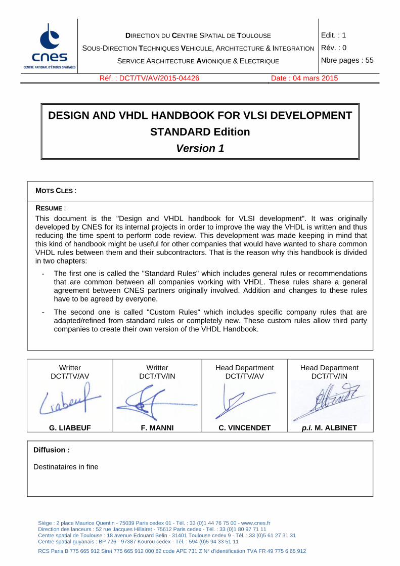
DESIGN AND VHDL HANDBOOK FOR VLSI DEVELOPMENT
STANDARD Edition
Version 1
MOTS CLES :
RESUME :
This document is the "Design and VHDL handbook for VLSI development". It was originally developed by CNES for its internal projects in order to improve the way the VHDL is written and thus reducing the time spent to perform code review. This development was made keeping in mind that this kind of handbook might be useful for other companies that would have wanted to share common VHDL rules between them and their subcontractors. That is the reason why this handbook is divided in two chapters:
- The first one is called the "Standard Rules" which includes general rules or recommendations that are common between all companies working with VHDL. These rules share a general agreement between CNES partners originally involved. Addition and changes to these rules have to be agreed by everyone.
- The second one is called "Custom Rules" which includes specific company rules that are adapted/refined from standard rules or completely new. These custom rules allow third party companies to create their own version of the VHDL Handbook.
Writter DCT/TV/AV
G. LIABEUF
Writter DCT/TV/IN
F. MANNI
Head Department DCT/TV/AV
C. VINCENDET
Head Department DCT/TV/IN
p.i. M. ALBINET
Diffusion : Destinataires in fine
DESIGN AND VHDL HANDBOOKFOR VLSI DEVELOPMENT
Standard Edition
Version 1 - 2015-03-04
Version 1 DESIGN AND VHDL HANDBOOKFOR VLSI DEVELOPMENT
2015-03-04
Release Notes Page ii
This PDF file is automatically created with Apache FOP version 1.1 from XML handbooks transformed with Saxonica XSLT saxon opensource version HE9-6-0-1J through IDE Eclipse Luna version "Luna Service Release 1 (4.4.1)" from Eclipse Foundation. All marks mentioned may be trademarks or registered trademarks of their respective owners. Apache FOP is licensed under the Apache License, Version 2.0. Saxon XSLT is licensed under the Mozilla Public License 1.0 (MPL), Mozilla Public License 2.0 (MPL 2.0) Eclipse Luna is licensed under the Eclipse Public License Version 1.0 Veditor is licensed under the Eclipse Public License, GNU General Public License version 2.0 (GPLv2)
Version 1 DESIGN AND VHDL HANDBOOKFOR VLSI DEVELOPMENT
2015-03-04
Table of Contents Page iii
Table of ContentsINTRODUCTION ............................................................................................................................................. 1GLOSSARY .................................................................................................................................................... 2VERSION HISTORY ........................................................................................................................................ 3STANDARD RULES ........................................................................................................................................ 4
1. Formatting ........................................................................................................................................... 41.1. Naming ..................................................................................................................................... 4
STD_00100 : VHDL object naming convention ............................................................................. 4STD_00200 : Name of clock signal ............................................................................................. 4STD_00300 : Name of reset signal .............................................................................................. 5STD_00400 : Label for process ................................................................................................... 5STD_00500 : Name of signal relation with behaviour ..................................................................... 6STD_00600 : VHDL file extension .............................................................................................. 6STD_00700 : Preservation of signal name ..................................................................................... 6STD_00800 : File name convention ............................................................................................. 7STD_00900 : File name of an entity ............................................................................................ 7
1.2. FileStructure .............................................................................................................................. 8STD_01000 : Number of entities per file ...................................................................................... 8STD_01100 : Number of architectures in files ............................................................................... 8STD_01200 : Number of statements per line ................................................................................. 9STD_01300 : Number of ports declaration per line ......................................................................... 9STD_01400 : Instantiation of components ................................................................................... 10STD_01500 : Entity ports convention ......................................................................................... 10STD_01600 : Entity port sort .................................................................................................... 11STD_01700 : Entity special ports ............................................................................................... 11STD_01800 : Primitive isolation ................................................................................................ 12STD_01900 : Indentation of source code ..................................................................................... 12STD_02000 : Indentation style .................................................................................................. 13STD_02100 : Compactness of VHDL source code ........................................................................ 13
2. Traceability ........................................................................................................................................ 142.1. Versioning ............................................................................................................................... 14
STD_02200 : Version control in header of file ............................................................................. 14STD_02300 : Copyright information in the header of file ............................................................... 14STD_02400 : Creation information in the header of the file ............................................................ 15STD_02500 : Functional information in the header of file .............................................................. 15
2.2. Reuse ...................................................................................................................................... 15STD_02600 : IEEE libraries preference ....................................................................................... 15STD_02700 : Default language .................................................................................................. 16STD_02800 : Comment strategy ................................................................................................ 16STD_02900 : Comments for entity ports ..................................................................................... 17STD_03000 : Comments for objects declaration and statements ....................................................... 17
2.3. Requirement ............................................................................................................................. 18STD_03100 : Dead VHDL code ................................................................................................ 18
3. Design ............................................................................................................................................... 193.1. I/O ......................................................................................................................................... 19
STD_03200 : Unused output ports components management ........................................................... 19STD_03300 : Buffer port type ................................................................................................... 19STD_03400 : Top level ports .................................................................................................... 20STD_03500 : Record type for top level entity ports ....................................................................... 20
3.2. Reset ...................................................................................................................................... 21STD_03600 : Reset sensitive level ............................................................................................. 21STD_03700 : Reset assertion and deassertion ............................................................................... 21STD_03800 : Synchronous elements initialization ......................................................................... 22
3.3. StateMachine ............................................................................................................................ 23STD_03900 : State machine type definition ................................................................................. 23STD_04000 : State machine case enumeration completion .............................................................. 23
Version 1 DESIGN AND VHDL HANDBOOKFOR VLSI DEVELOPMENT
2015-03-04
Table of Contents Page iv
3.4. Clocking .................................................................................................................................. 24STD_04100 : Clock domain crossing .......................................................................................... 24STD_04200 : Clock domain crossing handshake based .................................................................. 24STD_04300 : Clock domain crossing FIFOs based ........................................................................ 26STD_04400 : Clock management module .................................................................................... 27STD_04500 : Clock Reassignment ............................................................................................. 28STD_04600 : Clock domain number in the design ........................................................................ 29STD_04700 : Number of clock domains per modules .................................................................... 29STD_04800 : Clock edge sensitivity ........................................................................................... 30
3.5. Synchronous ............................................................................................................................. 30STD_04900 : Edge detection best practice ................................................................................... 31STD_05000 : Sensitivity list for synchronous processes ................................................................. 32STD_05100 : Metastability management ..................................................................................... 32STD_05200 : Output signal registration ...................................................................................... 33
3.6. Combinational .......................................................................................................................... 34STD_05300 : Sensitivity list for combinational processes ............................................................... 35STD_05400 : Unsuitability of internal tristate .............................................................................. 36STD_05500 : Unsuitability of latches ......................................................................................... 37STD_05600 : Unsuitability of combinational feedbacks ................................................................. 40STD_05700 : Unsuitability of gated clocks .................................................................................. 41
3.7. Type ....................................................................................................................................... 42STD_05800 : Use of VHDL types in RTL design ......................................................................... 42STD_05900 : Range for integers ................................................................................................ 43STD_06000 : Range direction for arrays ..................................................................................... 43STD_06100 : Range direction for std_logic_vector ....................................................................... 44STD_06200 : Management of numeric values .............................................................................. 44STD_06300 : Unsuitability of variables in RTL design .................................................................. 45
3.8. Reliability ................................................................................................................................ 45STD_06400 : Error mitigation strategy ....................................................................................... 45STD_06500 : Counters end of counting ...................................................................................... 46STD_06600 : Dimension of comparison elements ......................................................................... 46
3.9. Miscellaneous ........................................................................................................................... 47STD_06700 : Unsuitability of wait statement in RTL design ........................................................... 47STD_06800 : Unsuitability of signal initialization in declaration section ............................................ 47STD_06900 : Unsuitability of procedures and functions in RTL design ............................................. 48STD_07000 : Maximum depths of nested objects ......................................................................... 48
4. Simulation .......................................................................................................................................... 494.1. Miscellaneous ........................................................................................................................... 49
STD_07100 : Simulation ending ................................................................................................ 49STD_07200 : Use of procedures and functions in testbenches ......................................................... 49STD_07300 : Use of wait statement in testbenches ....................................................................... 50
Version 1 DESIGN AND VHDL HANDBOOKFOR VLSI DEVELOPMENT
2015-03-04
INTRODUCTION Page 1
INTRODUCTIONThis document is the "Design and VHDL handbook for VLSI development". It was originally developed by CNES for its internal projects in order to improve the way the VHDL is written and thus reducing the time spent to perform code review. This development was made keeping in mind that this kind of handbook might be useful for other companies that would have wanted to share common VHDL rules between them and their subcontractors. That is the reason why this handbook is divided in two chapters: - The first one is called the "Standard Rules" which includes general rules or recommendations that are common between all companies working with VHDL. These rules share a general agreement between CNES partners originally involved. Addition and changes to these rules have to be agreed by everyone. - The second one is called "Custom Rules" which includes specific company rules that are adapted/refined from standard rules or completely new. These custom rules allow third party companies to create their own version of the VHDL Handbook. A handbook is a collection of Rules written in XML following a specific schematic described inside a document called "VHDL handbook XML schema definition" (reference DCT-TV-IN-2014-9100). This XML file (or these XML files as there might be one standard and/or several customs ones) is the master source for this PDF file which is created automatically with an XSLT processor and FOP. The XML source file can be opened by any modern spreadsheet editor providing an easy and straightforward way to create applicability or verification matrix. Inside the XML handbook file, rules are identified with a unique ID number which is formatted as follows: LLL_DDDDD with L representing a Letter and D a Digit. Some three letters match is reserved like STD for standard rules and CNE for CNES specific rule (see DCT-TV-IN-2014-9100 for more reserved trigrams). A rule is part of a category/subcategory group and includes information like: a name, a short and long description, a rationale, good and bad VHDL examples, revision and even figures if needed. A rule is always associated with severity: - Major is selected when the rule is mandatory. Any deviation to a Major rule must be reported in a Non-Conformance Report and must be agreed by customer. - Minor is selected when the rule might lead to critical consequences. Non-conformance to a Minor rule can be approved in dedicated meeting, without Non-Conformance Report. - Note is selected when the rule is for information only. The handbook user is responsible for the application (or not) of this rule. It is usually best practices but not for every kind of situation. Some Rules might be sons of a parent rule. This was done to group unitary rules dealing with the same point. This notion was introduced to help company to easily tailor rule for compliance matrix has it is only mandatory to be compliant with the parent rule and not with each of its sons (nevertheless being compliant with the sons or equivalent custom sons rules is a good starting point to achieve compliance with the parent rule). Every one wishing to create a custom handbook can freely do so. This project was made with this strong concern in mind. You simply have to create a custom XML Ruleset following the schema describes in the document DCT-TV-IN-2014-9100. Nevertheless to work flawlessly with standard rules or others customs handbooks, the creator of a new Ruleset should better ask CNES for a reserved trigram letter identifying its company custom Rules. Authors of this handbook wish to thanks every (direct or indirect) contributor to this revision including: - People who agreed to share some of their internal knowledge to the benefit of everyone, - People who participated to the review of this document, - People who did the edition of this document, - People from W3C, Apache Software Foundation, Eclipse Foundation and creator of the Veditor plugin. Thank you all for being a precious part of this activity and making it exist.

Version 1 DESIGN AND VHDL HANDBOOKFOR VLSI DEVELOPMENT
2015-03-04
GLOSSARY Page 2
GLOSSARYASIC : Application Specific Integrated Circuit CNES : Centre National d'Etude Spatial (French Space Agency) CNE : Label for CNES rules FF : On figure, it means Flip-Flop FOP : Formatting Objects Processor FPGA : Field Programmable Gate Array PDF : Portable Document Format STD : Label for Standard Rules VLSI : Very Large Scale Integration VHDL : VHSIC Hardware Description Language XML : eXtensible Markup Language XSLT : eXtensible Stylesheet Language Transformations
Version 1 DESIGN AND VHDL HANDBOOKFOR VLSI DEVELOPMENT
2015-03-04
VERSION HISTORY Page 3
VERSION HISTORYVersion 1
Modification date 2015-03-04
Revision V1 : 2015-03-04 : Creation based on STD rule set V3 (2015-02-17)

Version 1 DESIGN AND VHDL HANDBOOKFOR VLSI DEVELOPMENT
2015-03-04
STANDARD RULES Page 4
STANDARD RULES
1. Formatting
1.1. Naming
STD_00100 : VHDL object naming convention
STD_00100 VHDL object naming convention Major
Revision 2 / 2014-12-01
Classification VLSI / Formatting / Naming
Application Field General
Parent Rule N/A
Description VHDL Object name definition use an unique and specific naming convention.
• Detailed Description:
This convention can address the naming of any the VHDL objects like signals, variables, constants, generic, labels, modules, entity....
• Rationale:
VHDL Object naming convention improves readability and reuse.
STD_00200 : Name of clock signal
STD_00200 Name of clock signal Major
Revision 3 / 2015-02-17
Classification VLSI / Formatting / Naming
Application Field General
Parent Rule STD_00100
Description The clock signal name includes "clk" or "clock".
• Detailed Description:
A signal is considered as a "CLOCK" whenever it is used to synchronize other signals to its rising or falling edge within a synchronous process with one of the following VHDL functions ('event, rising_edge or falling_edge), or when it is mapped on an IP clock input.
• Rationale:
The clock signal is critical. This signal needs to be easily found through the design.
• Good Example:
To be done for next release
• Bad Example:
Version 1 DESIGN AND VHDL HANDBOOKFOR VLSI DEVELOPMENT
2015-03-04
STANDARD RULES Page 5
To be done for next release
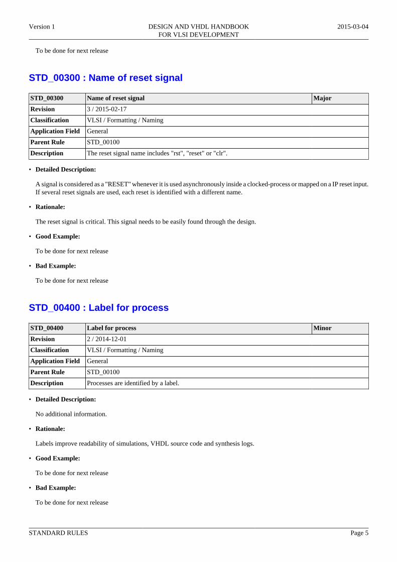
STD_00300 : Name of reset signal
STD_00300 Name of reset signal Major
Revision 3 / 2015-02-17
Classification VLSI / Formatting / Naming
Application Field General
Parent Rule STD_00100
Description The reset signal name includes "rst", "reset" or "clr".
• Detailed Description:
A signal is considered as a "RESET" whenever it is used asynchronously inside a clocked-process or mapped on a IP reset input.If several reset signals are used, each reset is identified with a different name.
• Rationale:
The reset signal is critical. This signal needs to be easily found through the design.
• Good Example:
To be done for next release
• Bad Example:
To be done for next release
STD_00400 : Label for process
STD_00400 Label for process Minor
Revision 2 / 2014-12-01
Classification VLSI / Formatting / Naming
Application Field General
Parent Rule STD_00100
Description Processes are identified by a label.
• Detailed Description:
No additional information.
• Rationale:
Labels improve readability of simulations, VHDL source code and synthesis logs.
• Good Example:
To be done for next release
• Bad Example:
To be done for next release

Version 1 DESIGN AND VHDL HANDBOOKFOR VLSI DEVELOPMENT
2015-03-04
STANDARD RULES Page 6
STD_00500 : Name of signal relation with behaviour
STD_00500 Name of signal relation with behaviour Minor
Revision 2 / 2014-12-01
Classification VLSI / Formatting / Naming
Application Field General
Parent Rule STD_00100
Description The signal name clearly identifies its purpose.
• Detailed Description:
A signal name is related to its functionality.For example a control signal (chip-select, write enable, read/output enable), an address, a counter, an enable, a pulse, a flag, acknowledge, ...
• Rationale:
A signal name related to its function improves the understanding of the code. It avoids miscomprehension by a peer readerand thus improves reliability of the code.
• Good Example:
To be done for next release
• Bad Example:
To be done for next release
STD_00600 : VHDL file extension
STD_00600 VHDL file extension Minor
Revision 3 / 2015-02-17
Classification VLSI / Formatting / Naming
Application Field General
Parent Rule N/A
Description The extension of VHDL source file is .vhd
• Detailed Description:
The extension of the VHDL file is ".vhd". The extension ".v" is reserved for verilog language. The extension ".vhdl" is not permitted.
• Rationale:
Same extension for each source file improves search and scripted automated actions.
STD_00700 : Preservation of signal name
STD_00700 Preservation of signal name Minor
Revision 3 / 2015-02-17
Version 1 DESIGN AND VHDL HANDBOOKFOR VLSI DEVELOPMENT
2015-03-04
STANDARD RULES Page 7
STD_00700 Preservation of signal name Minor
Classification VLSI / Formatting / Naming
Application Field General
Parent Rule N/A
Description A non modified signal keeps its name through hierarchy levels.
• Detailed Description:
Important signals like reset or clock have to keep their name across hierarchy. It is a best practise for other signals not to change their name if they are not altered by any kind of logic.
• Rationale:
There is no needs to change a name of a signal if this signal doesn't change. Renaming of important signal (like clock or reset)can lead to simulation mismatch. Moreover, changing a name of a signal which is not altered makes the understanding ofthe code more difficult.
• Good Example:
To be done for next release
• Bad Example:
To be done for next release
STD_00800 : File name convention
STD_00800 File name convention Minor
Revision 3 / 2015-02-17
Classification VLSI / Formatting / Naming
Application Field General
Parent Rule N/A
Description File name uses an unique and specific naming convention within a design.
• Detailed Description:
No additional information.
• Rationale:
File name coherency improves search and scripted automated actions.
STD_00900 : File name of an entity
STD_00900 File name of an entity Minor
Revision 3 / 2015-02-17
Classification VLSI / Formatting / Naming
Application Field General
Parent Rule STD_00800
Description The file name for an entity VHDL file includes at least the entity name.
Version 1 DESIGN AND VHDL HANDBOOKFOR VLSI DEVELOPMENT
2015-03-04
STANDARD RULES Page 8
• Detailed Description:
File name of an entity called MyEntity is : (Any characters)MyEntity(Any characters).vhd
• Rationale:
The match between file name and entity name improves the research for an entity inside a project.
1.2. FileStructure
STD_01000 : Number of entities per file
STD_01000 Number of entities per file Major
Revision 3 / 2015-02-17
Classification VLSI / Formatting / FileStructure
Application Field General
Parent Rule N/A
Description Each source file contains only one VHDL entity.
• Detailed Description:
No additional information.
• Rationale:
A single entity by file avoids compilation or synthesis ordering problems. It improves search of the file including a specificentity.
• Good Example:
To be done for next release
• Bad Example:
To be done for next release
STD_01100 : Number of architectures in files
STD_01100 Number of architectures in files Major
Revision 2 / 2014-12-01
Classification VLSI / Formatting / FileStructure
Application Field General
Parent Rule N/A
Description Each VHDL file includes only one architecture per file.
• Detailed Description:
No additional information.
• Rationale:
Version 1 DESIGN AND VHDL HANDBOOKFOR VLSI DEVELOPMENT
2015-03-04
STANDARD RULES Page 9
When the design is synthesized, only one architecture is synthesized for each synthesized entity. Including only one architectureper file reduce a potential architecture selection error at synthesis level.
• Good Example:
To be done for next release
• Bad Example:
To be done for next release
STD_01200 : Number of statements per line
STD_01200 Number of statements per line Major
Revision 2 / 2014-12-01
Classification VLSI / Formatting / FileStructure
Application Field General
Parent Rule N/A
Description A line includes only one statement.
• Detailed Description:
A statement could be an affectation sequence, a conditional test, a declaration or a VHDL beginning sequence like case, process...).
• Rationale:
A single statement per line improves readability and maintainability.
• Good Example:
To be done for next release
• Bad Example:
To be done for next release
STD_01300 : Number of ports declaration per line
STD_01300 Number of ports declaration per line Major
Revision 3 / 2015-02-17
Classification VLSI / Formatting / FileStructure
Application Field General
Parent Rule N/A
Description A line includes only one port definition or mapping.
• Detailed Description:
No additional information.
• Rationale:
Version 1 DESIGN AND VHDL HANDBOOKFOR VLSI DEVELOPMENT
2015-03-04
STANDARD RULES Page 10
A single port declaration per line improves readability.
• Good Example:
To be done for next release
• Bad Example:
To be done for next release
STD_01400 : Instantiation of components
STD_01400 Instantiation of components Major
Revision 3 / 2015-02-17
Classification VLSI / Formatting / FileStructure
Application Field General
Parent Rule N/A
Description The instantiation of components is made by name.
• Detailed Description:
Since instantiation is made by name, the instantiation by position is prohibited.This rule does not apply to instantiations made within IP cores would they be coming auto generated from a tool or provided by any IP core provider.
• Rationale:
Instantiation by name improves readability as there is not need to look to the entity definition to know the connection betweenport and signal. It reduces risks of inconsistency between the entity definition and the component instantiation in case of entitymodification.
• Good Example:
To be done for next release
• Bad Example:
To be done for next release
STD_01500 : Entity ports convention
STD_01500 Entity ports convention Major
Revision 2 / 2014-12-01
Classification VLSI / Formatting / FileStructure
Application Field General
Parent Rule N/A
Description Entity ports are organized with a dedicated convention.
• Detailed Description:
This convention deals with the way the ports of an entity are sorted: by direction, interface, special signals...

Version 1 DESIGN AND VHDL HANDBOOKFOR VLSI DEVELOPMENT
2015-03-04
STANDARD RULES Page 11
• Rationale:
Ports declaration strategy allows readability and reuse.
• Good Example:
To be done for next release
• Bad Example:
To be done for next release
STD_01600 : Entity port sort
STD_01600 Entity port sort Minor
Revision 3 / 2015-02-17
Classification VLSI / Formatting / FileStructure
Application Field General
Parent Rule STD_01500
Description Entity ports are organized by interface.
• Detailed Description:
Entity ports are grouped by external interfaces.Within an interface group, ports could then be sorted by direction (input, output, bidirectional).
• Rationale:
Ports grouped by external interfaces improves readability.
• Good Example:
To be done for next release
• Bad Example:
To be done for next release
STD_01700 : Entity special ports
STD_01700 Entity special ports Minor
Revision 3 / 2015-02-17
Classification VLSI / Formatting / FileStructure
Application Field General
Parent Rule STD_01500
Description Special ports are the first group of an entity.
• Detailed Description:
Special input ports like clock(s), reset and global enable are the first to be written for an entity.
• Rationale:
Version 1 DESIGN AND VHDL HANDBOOKFOR VLSI DEVELOPMENT
2015-03-04
STANDARD RULES Page 12
These specials signals are important for the understanding of the module functionalities. Thus gathering them at the beginningof an entity improves readability.
• Good Example:
To be done for next release
• Bad Example:
To be done for next release
STD_01800 : Primitive isolation
STD_01800 Primitive isolation Minor
Revision 3 / 2015-02-17
Classification VLSI / Formatting / FileStructure
Application Field General
Parent Rule N/A
Description Primitive are isolated in a wrapper entity defined in a dedicated VHDL file.
• Detailed Description:
When an IP core is used (memory inference/instantiation, primitives instantiations like PLLs, etc…), then the generated HDL code is manufacturer/technology specific.It is best practice to separate this code from the general HDL code, which is not specific to the manufacturer/technology, by creating a more generic wrapper which contains all those specific HDL codes.
• Rationale:
Specific or primitive IP cores are technology dependent. Isolating these IP improves technology retargeting.
STD_01900 : Indentation of source code
STD_01900 Indentation of source code Minor
Revision 3 / 2015-02-17
Classification VLSI / Formatting / FileStructure
Application Field General
Parent Rule N/A
Description VHDL source file is indented.
• Detailed Description:
No additional information.
• Rationale:
Proper indentation improves readability.
• Good Example:
To be done for next release
Version 1 DESIGN AND VHDL HANDBOOKFOR VLSI DEVELOPMENT
2015-03-04
STANDARD RULES Page 13
• Bad Example:
To be done for next release
STD_02000 : Indentation style
STD_02000 Indentation style Minor
Revision 2 / 2014-12-01
Classification VLSI / Formatting / FileStructure
Application Field General
Parent Rule STD_01900
Description Indentation is made by a fixed number of blank spaces instead of tabulation.
• Detailed Description:
No additional information.
• Rationale:
Text editors display hard tabs differently. When a designer uses only spaces, the sources code formatting is independent ofthe text editors used.
• Good Example:
To be done for next release
• Bad Example:
To be done for next release
STD_02100 : Compactness of VHDL source code
STD_02100 Compactness of VHDL source code Minor
Revision 3 / 2015-02-17
Classification VLSI / Formatting / FileStructure
Application Field General
Parent Rule N/A
Description Hand coded VHDL source files are limited in size.
• Detailed Description:
File limitation strategy might be implemented with a limit of lines, name characters, entity's names length, compact signal name,...
• Rationale:
Hand coded VHDL source files limited in size keep the module less complicated and thus easier to validate and read. Moreover, some tools do not handle well too many characters per lines.
Version 1 DESIGN AND VHDL HANDBOOKFOR VLSI DEVELOPMENT
2015-03-04
STANDARD RULES Page 14
2. Traceability
2.1. Versioning
STD_02200 : Version control in header of file
STD_02200 Version control in header of file Major
Revision 3 / 2015-02-17
Classification VLSI / Traceability / Versioning
Application Field General
Parent Rule N/A
Description VHDL file includes information that tracks and provides control over changes to source code.
• Detailed Description:
The revision control mechanism is written in the header file which then includes: - Version Tag (number, letter...), - Author, - Date of modification, - Author of modification, - Description of modification, - Reason of modification, - Impacts of modification, - The file creation date, - Current version number.Large VHDL project could use version control document software (like SVN), if this is the case a tag identifying the version is also included.
• Rationale:
Version control insures that development history is saved so that a new developer could use it and avoid previous mistakeor understand previous choices. Understanding the last modifications allows integrator to know if a bug was corrected or ifthe modification will produce a problem.
• Good Example:
To be done for next release
• Bad Example:
To be done for next release
STD_02300 : Copyright information in the header of file
STD_02300 Copyright information in the header of file Minor
Revision 2 / 2014-12-01
Classification VLSI / Traceability / Versioning
Application Field General
Parent Rule N/A
Description Header of the file includes Copyright information.
Version 1 DESIGN AND VHDL HANDBOOKFOR VLSI DEVELOPMENT
2015-03-04
STANDARD RULES Page 15
• Detailed Description:
The copyright information includes: - A license restriction (if needed), - The name of the company owning the rights, - The VHDL designer company if the design is subcontracted.
• Rationale:
These information ensure that the VHDL file is not reused, disclosed if it is not allowed.
STD_02400 : Creation information in the header of the file
STD_02400 Creation information in the header of the file Minor
Revision 2 / 2015-02-17
Classification VLSI / Traceability / Versioning
Application Field General
Parent Rule N/A
Description HDL file includes a header with specific information.
• Detailed Description:
Typical information that can be included in the header are: file name, author, creation date, project name, software context.
• Rationale:
A common header format which gathers all important information for each HDL file improves the understanding of vhdlbackground context of the developed module.
STD_02500 : Functional information in the header of file
STD_02500 Functional information in the header of file Minor
Revision 1 / 2014-12-01
Classification VLSI / Traceability / Versioning
Application Field General
Parent Rule N/A
Description Header of File includes information about code functionality.
• Detailed Description:
Functional description could be, for example, a short description of the file functions, its limitations or a description of the naming convention used.
• Rationale:
Functional information in the file header improves understanding of the code function while reviewing of reusing it.
2.2. Reuse
STD_02600 : IEEE libraries preference

Version 1 DESIGN AND VHDL HANDBOOKFOR VLSI DEVELOPMENT
2015-03-04
STANDARD RULES Page 16
STD_02600 IEEE libraries preference Major
Revision 3 / 2015-02-17
Classification VLSI / Traceability / Reuse
Application Field General
Parent Rule N/A
Description Use the following IEEE libraries : "std_logic_1164" and "numeric_std"
• Detailed Description:
Do not use deprecated Synopsis libraries "std_logic_arith", "std_logic_signed" and "std_logic_unsigned" except if you are targeting specifically a Synopsys synthesizer (like for ASIC for instance).Nevertheless, never mix these two library families.
• Rationale:
Using standardized libraries by IEEE improves code portability. "std_logic_arith", "std_logic_signed" and"std_logic_unsigned" libraries are not standardized.
STD_02700 : Default language
STD_02700 Default language Minor
Revision 3 / 2015-02-17
Classification VLSI / Traceability / Reuse
Application Field General
Parent Rule N/A
Description Header, instructions and comments are written in English.
• Detailed Description:
No additional information.
• Rationale:
English language usage allows readability and reuse by a broader group (including an international designer community).
STD_02800 : Comment strategy
STD_02800 Comment strategy Minor
Revision 3 / 2015-02-17
Classification VLSI / Traceability / Reuse
Application Field General
Parent Rule N/A
Description The VHDL code includes comments.
• Detailed Description:
The VHDL code comments need to explain the purposes and objectives of the code as much as possible, but not describe the code.
• Rationale:
Version 1 DESIGN AND VHDL HANDBOOKFOR VLSI DEVELOPMENT
2015-03-04
STANDARD RULES Page 17
Relevant comments increase readability of the code.
STD_02900 : Comments for entity ports
STD_02900 Comments for entity ports Minor
Revision 3 / 2015-02-17
Classification VLSI / Traceability / Reuse
Application Field General
Parent Rule STD_02800
Description Each entity port is commented with a short functional description.
• Detailed Description:
No additional information.
• Rationale:
Comments on ports allow the IP integrator to quickly identify port connections when instantiating the modules.
• Good Example:
To be done for next release
• Bad Example:
To be done for next release
STD_03000 : Comments for objects declaration and statements
STD_03000 Comments for objects declaration and statements Minor
Revision 3 / 2015-02-17
Classification VLSI / Traceability / Reuse
Application Field General
Parent Rule STD_02800
Description Each process, group of instructions and objects declaration are commented
• Detailed Description:
No additional information.
• Rationale:
Accurate and up-to-date comments increase readability, reuse and understanding
• Good Example:
To be done for next release
• Bad Example:
To be done for next release
Version 1 DESIGN AND VHDL HANDBOOKFOR VLSI DEVELOPMENT
2015-03-04
STANDARD RULES Page 18
2.3. Requirement
STD_03100 : Dead VHDL code
STD_03100 Dead VHDL code Major
Revision 3 / 2015-02-17
Classification VLSI / Traceability / Requirement
Application Field General
Parent Rule N/A
Description Unnecessary portions of code is deleted
• Detailed Description:
Unused declared signals and constants are deleted. Inactive or wrong code are deleted. Pieces of code commented out doesn't appear in HDL sources.
• Rationale:
Unnecessary portions of code deleted improve code coverage results and make the design more robust.
• Good Example:
To be done for next release
• Bad Example:
To be done for next release
Version 1 DESIGN AND VHDL HANDBOOKFOR VLSI DEVELOPMENT
2015-03-04
STANDARD RULES Page 19
3. Design
3.1. I/O
STD_03200 : Unused output ports components management
STD_03200 Unused output ports components management Major
Revision 2 / 2014-12-01
Classification VLSI / Design / I/O
Application Field General
Parent Rule N/A
Description Unused output ports are mapped with the keyword "open".
• Detailed Description:
No additional information.
• Rationale:
The keyword "open" is preferred to the connection of an unused output port to a dummy signal which causes implicit netconnection during synthesis.
• Good Example:
To be done for next release
• Bad Example:
To be done for next release
STD_03300 : Buffer port type
STD_03300 Buffer port type Major
Revision 2 / 2014-12-01
Classification VLSI / Design / I/O
Application Field General
Parent Rule N/A
Description "Buffer" port in an entity is forbidden.
• Detailed Description:
Reading an output signal inside an entity can be achieved by created an internal signal.
• Rationale:
VHDL authorize entity I/O to be of type in, out, inout or buffer. Buffer authorizes an output of an entity to be read inside theentity. Manufacturers of synthesis software do not recommend "buffer" type usage because buffers may give some problemsduring synthesis.
• Good Example:
Version 1 DESIGN AND VHDL HANDBOOKFOR VLSI DEVELOPMENT
2015-03-04
STANDARD RULES Page 20
To be done for next release
• Bad Example:
To be done for next release
STD_03400 : Top level ports
STD_03400 Top level ports Major
Revision 2 / 2014-12-01
Classification VLSI / Design / I/O
Application Field General
Parent Rule N/A
Description Top level ports include approved types.
• Detailed Description:
When designing the TOP level, the designer uses only types which are allowed. Every types which are not in the allowed list are prohibited to use.
• Rationale:
Top level entity ports are mapped on real component pins. Thus, restrictions apply to be sure that these VHDL pins mapflawlessly to real pins.
• Good Example:
To be done for next release
• Bad Example:
To be done for next release
STD_03500 : Record type for top level entity ports
STD_03500 Record type for top level entity ports Major
Revision 3 / 2015-02-17
Classification VLSI / Design / I/O
Application Field General
Parent Rule STD_03400
Description Record type is forbidden for top level entity ports.
• Detailed Description:
No additional information.
• Rationale:
Top level entity ports are mapped on real component pins. Thus, restrictions apply to be sure that these VHDL pins mapflawlessly to real pins.
• Good Example:
Version 1 DESIGN AND VHDL HANDBOOKFOR VLSI DEVELOPMENT
2015-03-04
STANDARD RULES Page 21
To be done for next release
• Bad Example:
To be done for next release
3.2. Reset
STD_03600 : Reset sensitive level
STD_03600 Reset sensitive level Major
Revision 3 / 2015-02-17
Classification FPGA / Design / Reset
Application Field General
Parent Rule N/A
Description Every synchronous process uses the same reset activation level.
• Detailed Description:
No additional information.
• Rationale:
In an FPGA, the reset signal is usually a high fan-out signal routed using a dedicated global signal routing track. Using bothlevels of the reset signal to asynchronously reset the flip-flops of the design results in the synthesis of the reset signal itselfand its inverted version, which leads to the usage of 2 global dedicated routing tracks versus a single one, with one of thereset signal passing through an inverter in the FPGA fabric rendering the reset recovery timings closure harder to meet forthe FPGA EDA tools.
• Good Example:
To be done for next release
• Bad Example:
To be done for next release
STD_03700 : Reset assertion and deassertion
STD_03700 Reset assertion and deassertion Major
Revision 3 / 2015-02-17
Classification VLSI / Design / Reset
Application Field General
Parent Rule N/A
Description Internal reset is asserted asynchronously and deasserted synchronously.
• Detailed Description:
If several clock domains are used then several reset signals are created to be deasserted synchronously with each targeted clock domain.
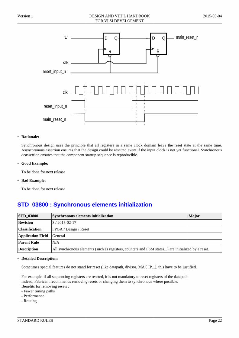
• Figure:
Version 1 DESIGN AND VHDL HANDBOOKFOR VLSI DEVELOPMENT
2015-03-04
STANDARD RULES Page 22
D D QQ
RR
clk
reset_input_n
'1' main_reset_n
clk
reset_input_n
main_reset_n
• Rationale:
Synchronous design uses the principle that all registers in a same clock domain leave the reset state at the same time.Asynchronous assertion ensures that the design could be resetted event if the input clock is not yet functional. Synchronousdeassertion ensures that the component startup sequence is reproducible.
• Good Example:
To be done for next release
• Bad Example:
To be done for next release
STD_03800 : Synchronous elements initialization
STD_03800 Synchronous elements initialization Major
Revision 3 / 2015-02-17
Classification FPGA / Design / Reset
Application Field General
Parent Rule N/A
Description All synchronous elements (such as registers, counters and FSM states...) are initialized by a reset.
• Detailed Description:
Sometimes special features do not stand for reset (like datapath, divisor, MAC IP...), this have to be justified. For example, if all sequencing registers are reseted, it is not mandatory to reset registers of the datapath.Indeed, Fabricant recommends removing resets or changing them to synchronous where possible.Benefits for removing resets :- Fewer timing paths- Performance- Routing

Version 1 DESIGN AND VHDL HANDBOOKFOR VLSI DEVELOPMENT
2015-03-04
STANDARD RULES Page 23
- InferencingBenefits for changing resets to synchronous :- Improved use of dedicated register functions- More flexible register placement- More predictable timing and circuit operation
• Rationale:
Initialisation of synchronous elements contribute to deterministic reset behaviour and simulation match between functionaland Post-Place and Route.
• Good Example:
To be done for next release
• Bad Example:
To be done for next release
3.3. StateMachine
STD_03900 : State machine type definition
STD_03900 State machine type definition Major
Revision 2 / 2014-12-01
Classification VLSI / Design / StateMachine
Application Field General
Parent Rule N/A
Description FSM states are encoded using enumerated type.
• Detailed Description:
Others type of state machine definition like vectors or integer are forbidden.
• Rationale:
Enumerated type to encode FSM states allows readability and reuse.
• Good Example:
To be done for next release
• Bad Example:
To be done for next release
STD_04000 : State machine case enumeration completion
STD_04000 State machine case enumeration completion Major
Revision 2 / 2014-12-01
Classification VLSI / Design / StateMachine
Application Field General
Parent Rule N/A
Version 1 DESIGN AND VHDL HANDBOOKFOR VLSI DEVELOPMENT
2015-03-04
STANDARD RULES Page 24
STD_04000 State machine case enumeration completion Major
Description VHDL code addresses all the defined states of the state machine.
• Detailed Description:
When all cases statement are not explicitly addressed in the VHDL code, an extra "when others" case will be added."when others" instruction handles the default condition when none of the previous case statements are met.
• Rationale:
State completion ensures deterministic behaviour between simulation and final design.
• Good Example:
To be done for next release
• Bad Example:
To be done for next release
3.4. Clocking
STD_04100 : Clock domain crossing
STD_04100 Clock domain crossing Major
Revision 3 / 2015-02-17
Classification VLSI / Design / Clocking
Application Field General
Parent Rule N/A
Description All data exchanges between different clock domains are done with specific approved mechanism.
• Detailed Description:
No additional information.
• Rationale:
Changing clock domains can lead data incoherency or data loss due to metastability. These effects will mainly be seen on theintegrated system. The use of a validated clock domain change mechanism reduce the risk of discrepancies.
STD_04200 : Clock domain crossing handshake based
STD_04200 Clock domain crossing handshake based Note
Revision 3 / 2015-02-17
Classification VLSI / Design / Clocking
Application Field General
Parent Rule STD_04100
Description Clock domain crosses uses a handshaked based synchronizer.
• Detailed Description:
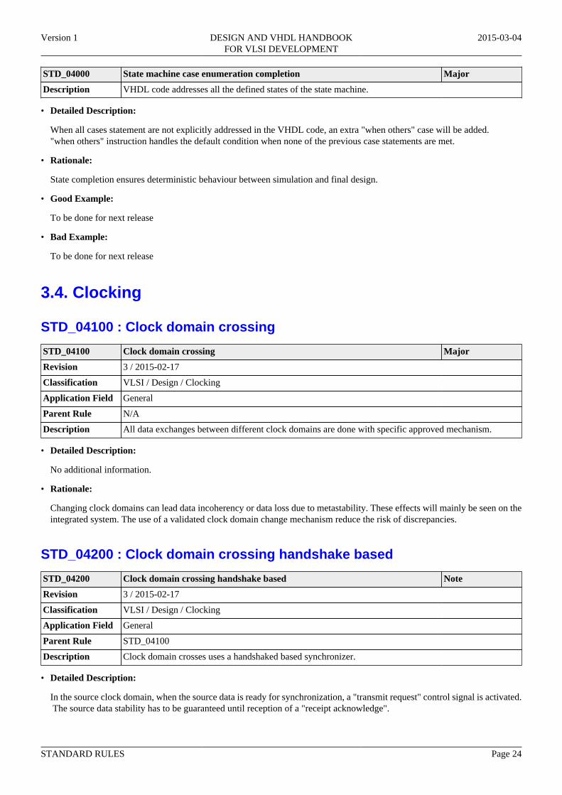
In the source clock domain, when the source data is ready for synchronization, a "transmit request" control signal is activated. The source data stability has to be guaranteed until reception of a "receipt acknowledge".
Version 1 DESIGN AND VHDL HANDBOOKFOR VLSI DEVELOPMENT
2015-03-04
STANDARD RULES Page 25
In the destination clock domain, the "transmit request" control signal is synchronized using a double or triple register synchronization technique.It is then used to sample the data to synchronize in the destination clock domain. A "receipt acknowledge" is then sent back to the source clock domain. In the source clock domain, the "receipt acknowledge" is synchronized using a double or triple register synchronization technique.The source data can now be changed and another synchronization handshake can be initiated."transmit request" and "receipt acknowledge" data stability for the m-registers synchronizers: - data values must be stable for m+1 destination clock cycles.Source data stability: - The source data must be present when "transmit request" is asserted on the destination and remain stable until the "receipt acknowledge" is generated.The source clock domain should continue to assert the "transmit request" control signal until "receipt acknowledge" is asserted at the source clock domain.The sender should not assert a new "transmit request" until the acknowledgement for the previous transfer is de-asserted in the source clock domain.
• Figure:
Q D Q
DQ
clk_b
clk_a
request_r2request
grant_r2DQ
D
grant
clk_a
request
grant_r2
clk_b
request_r2
Source Destination
request_r
grant_r
grant
data
• Rationale:
Version 1 DESIGN AND VHDL HANDBOOKFOR VLSI DEVELOPMENT
2015-03-04
STANDARD RULES Page 26
Using the proper clock domain crossing technique to pass a data bus from one clock domain to another is critical in orderto ensure a proper behaviour of the design under any circumstances. When the data to synchronize is a data bus or can beconsidered as one, and that the high latency of the handshaked based synchronizer can be tolerated, then dual handshakedsynchronizer technique is appropriate.
• Good Example:
To be done for next release
• Bad Example:
To be done for next release
STD_04300 : Clock domain crossing FIFOs based
STD_04300 Clock domain crossing FIFOs based Note
Revision 3 / 2015-02-17
Classification VLSI / Design / Clocking
Application Field General
Parent Rule STD_04100
Description Clock domain crosses uses a dual clock FIFO based synchronizer.
• Detailed Description:
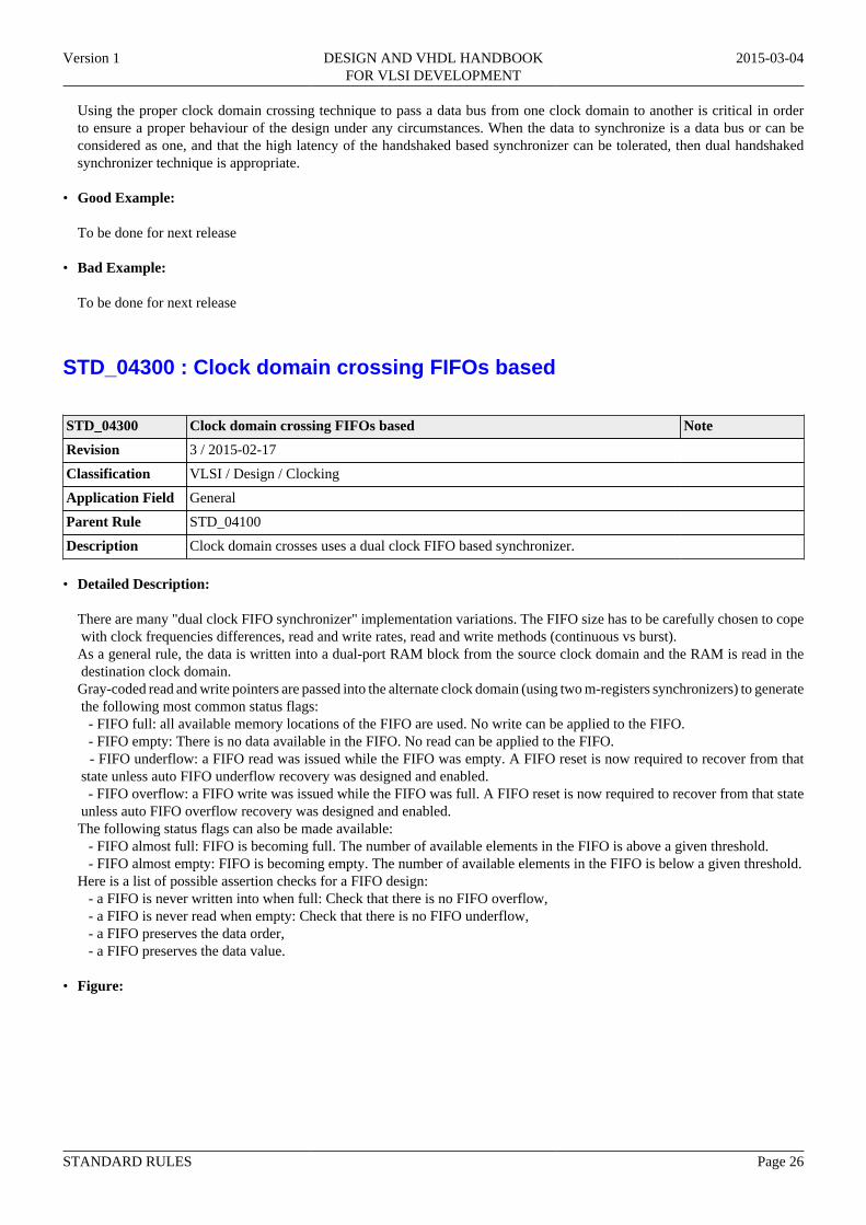
There are many "dual clock FIFO synchronizer" implementation variations. The FIFO size has to be carefully chosen to cope with clock frequencies differences, read and write rates, read and write methods (continuous vs burst).As a general rule, the data is written into a dual-port RAM block from the source clock domain and the RAM is read in the destination clock domain.Gray-coded read and write pointers are passed into the alternate clock domain (using two m-registers synchronizers) to generate the following most common status flags: - FIFO full: all available memory locations of the FIFO are used. No write can be applied to the FIFO. - FIFO empty: There is no data available in the FIFO. No read can be applied to the FIFO. - FIFO underflow: a FIFO read was issued while the FIFO was empty. A FIFO reset is now required to recover from that state unless auto FIFO underflow recovery was designed and enabled. - FIFO overflow: a FIFO write was issued while the FIFO was full. A FIFO reset is now required to recover from that state unless auto FIFO overflow recovery was designed and enabled.The following status flags can also be made available: - FIFO almost full: FIFO is becoming full. The number of available elements in the FIFO is above a given threshold. - FIFO almost empty: FIFO is becoming empty. The number of available elements in the FIFO is below a given threshold.Here is a list of possible assertion checks for a FIFO design: - a FIFO is never written into when full: Check that there is no FIFO overflow, - a FIFO is never read when empty: Check that there is no FIFO underflow, - a FIFO preserves the data order, - a FIFO preserves the data value.
• Figure:

Version 1 DESIGN AND VHDL HANDBOOKFOR VLSI DEVELOPMENT
2015-03-04
STANDARD RULES Page 27
writeprocess
readprocess
s_wr_en d_rd_en
d_rd_datas_wr_data
clks clkd
FiFo
din dout
wr_en
empty
full
used
empty
full
used
n n
rd_en
wr_clk rd_clk
nn
• Rationale:
Utilizing the proper clock domain crossing technique to pass a data bus from one clock domain to another is critical in orderto ensure a proper behaviour of the design under any circumstances. When the data to synchronize is a data bus or canbe considered as one, that the synchronization rate is fast, and that the high latency of a handshaked based synchronizercannot be tolerated, then dual clock FIFO synchronizer technique (if available in the component) is appropriate. The FIFOimplementation ensures data order and data content preservation.
STD_04400 : Clock management module
STD_04400 Clock management module Major
Revision 3 / 2015-02-17
Classification VLSI / Design / Clocking
Application Field General
Parent Rule N/A
Description All global clocks are generated in a single dedicated module.
• Detailed Description:
Any clock element inserted in any clock path is instantiated inside the same design entity. Clock elements are clock buffers, clock multiplexers, PLLs, DCMs, fractional dividers, gapped clock logic, enabled clock logic...
• Figure:

Version 1 DESIGN AND VHDL HANDBOOKFOR VLSI DEVELOPMENT
2015-03-04
STANDARD RULES Page 28
clk
Top level
CMM
Module A
Module Bclkb
clka
Use single Clock Management Module instead
Top levelModule A
Module B
clk
CMM
CMM clka
clkb
• Rationale:
A dedicated clock module is essential to design for reuse and design portability, while improving clocks identificationand management throughout the design. Such a practice isolates all vendor-specific clocking elements such as PLLs, clockmultiplexers and clock buffers in a single instance that can be easily replaced to target another technology from the samevendor or not. Thereby, a FPGA prototype design can be easily ported to another FPGA family or an ASIC technology.
• Good Example:
To be done for next release
• Bad Example:
To be done for next release
STD_04500 : Clock Reassignment
STD_04500 Clock Reassignment Major
Revision 1 / 2015-02-17
Classification VLSI / Design / Clocking
Application Field General
Version 1 DESIGN AND VHDL HANDBOOKFOR VLSI DEVELOPMENT
2015-03-04
STANDARD RULES Page 29
STD_04500 Clock Reassignment Major
Parent Rule N/A
Description Do not reassign a clock in a concurrent statement.
• Detailed Description:
No additional information.
• Rationale:
Using of only one signal or one port for clock avoids multiple net names for the same clock signal will ease the fitter to matchthe clock network on the dedicated low skew resources.
• Good Example:
To be done for next release
• Bad Example:
To be done for next release
STD_04600 : Clock domain number in the design
STD_04600 Clock domain number in the design Minor
Revision 2 / 2015-02-17
Classification FPGA / Design / Clocking
Application Field General
Parent Rule N/A
Description One clock domain is used in the design.
• Detailed Description:
The number of timing domains is reduced as far as reasonably possible : one single clock domain design is the target.When a slower clock version is needed use an enable signal instead of a derived clock to throttle the resulting clock rate.When a faster clock version is needed, promote that faster clock as the single clock domain used if the design and or re-design consequences are not prohibitive prior to creating a derived clock domain.
• Rationale:
Reducing the number of clock domain in a design is critical in order to keep the number of clock domains crossing resolutionsto few manageable cases. Doing so limits the chance for clock domain crossing design issues, limits the number of nets notcovered with static timing analysis and simplifies greatly the synthesis scripts. For those reasons, usage of a single clockdomain is strongly recommended.
• Good Example:
To be done for next release
• Bad Example:
To be done for next release
STD_04700 : Number of clock domains per modules
STD_04700 Number of clock domains per modules Minor
Revision 3 / 2015-02-17

Version 1 DESIGN AND VHDL HANDBOOKFOR VLSI DEVELOPMENT
2015-03-04
STANDARD RULES Page 30
STD_04700 Number of clock domains per modules Minor
Classification FPGA / Design / Clocking
Application Field General
Parent Rule N/A
Description Each module in the design handle only one clock.
• Detailed Description:
Entity that is linked between entities can have several clocks at input but do not manage processes on those clocks.The only module that can handle several clocks are the clock management modules and the reset management module.Others module can includes different clocks but the data exchange between them is done through the approved clock domain crossing module.
• Rationale:
Separating the clock domains in the design architecture greatly improves the clock domains identifications, the data flowunderstanding and most importantly allows fast tracing of the clock domain crossing signals that need special design and statictiming analysis considerations while enabling better design reuse.
• Good Example:
To be done for next release
• Bad Example:
To be done for next release
STD_04800 : Clock edge sensitivity
STD_04800 Clock edge sensitivity Minor
Revision 2 / 2014-12-01
Classification FPGA / Design / Clocking
Application Field General
Parent Rule N/A
Description A unique single sensitive edge is used to clock all Flip-Flop in the same clock domain.
• Detailed Description:
No additional information.
• Rationale:
Use of a single clock sensitive edge allows efficient timing analysis. Using only one edge of a clock allows to avoid over-constrain static timing analysis. Moreover, the design isn't duty cycle sensitive.
• Good Example:
To be done for next release
• Bad Example:
To be done for next release
3.5. Synchronous
Version 1 DESIGN AND VHDL HANDBOOKFOR VLSI DEVELOPMENT
2015-03-04
STANDARD RULES Page 31
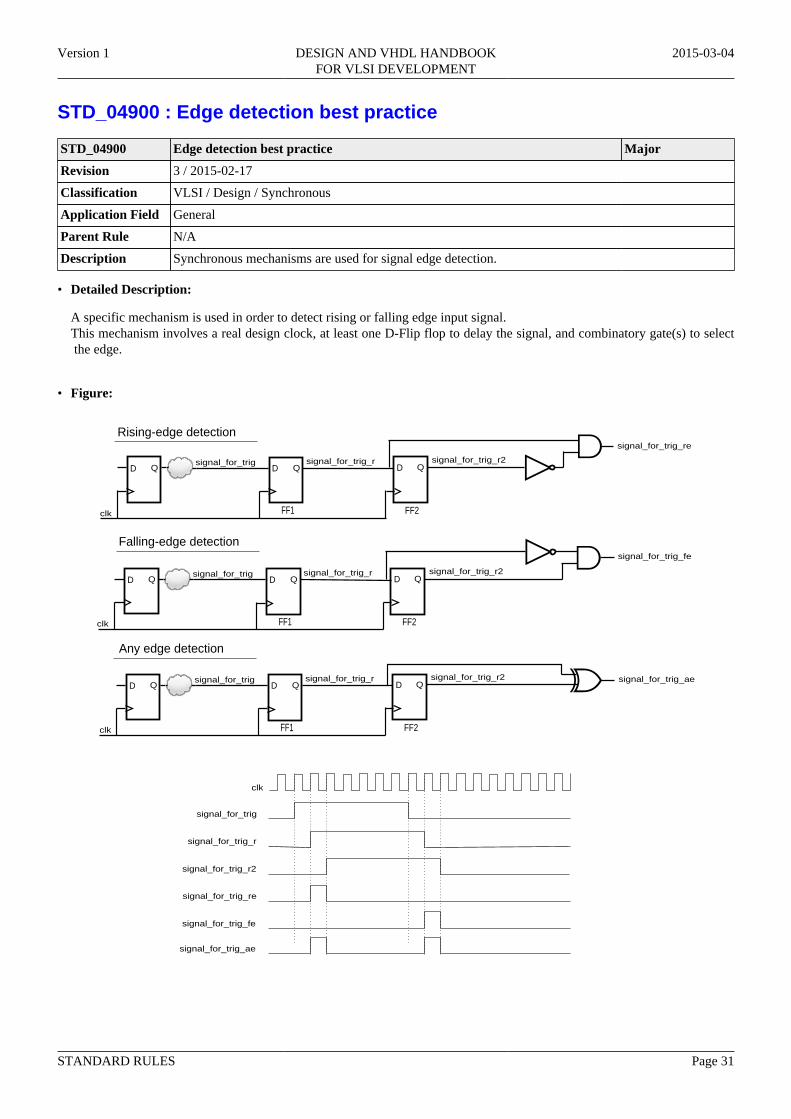
STD_04900 : Edge detection best practice
STD_04900 Edge detection best practice Major
Revision 3 / 2015-02-17
Classification VLSI / Design / Synchronous
Application Field General
Parent Rule N/A
Description Synchronous mechanisms are used for signal edge detection.
• Detailed Description:
A specific mechanism is used in order to detect rising or falling edge input signal.This mechanism involves a real design clock, at least one D-Flip flop to delay the signal, and combinatory gate(s) to select the edge.
• Figure:
Any edge detection
Falling-edge detection
QD D DQ Q
Rising-edge detection
FF2FF1clk
signal_for_trig signal_for_trig_r signal_for_trig_r2
signal_for_trig_re
QD D DQ Q
FF2FF1clk
signal_for_trig signal_for_trig_r signal_for_trig_r2
QD D DQ Q
FF2FF1clk
signal_for_trig signal_for_trig_r signal_for_trig_r2
signal_for_trig_fe
signal_for_trig_ae
clk
signal_for_trig
signal_for_trig_r
signal_for_trig_r2
signal_for_trig_re
signal_for_trig_fe
signal_for_trig_ae
Version 1 DESIGN AND VHDL HANDBOOKFOR VLSI DEVELOPMENT
2015-03-04
STANDARD RULES Page 32
• Rationale:
Flip flops clock input is dedicated to a clock signal. Thus, using it as a way to detect a signal edge (by using rising_edge(...)or 'event attribute) may lead to the creation of a new clock domain for each signal edge detection implemented in the design:this is not the purpose.
• Good Example:
To be done for next release
• Bad Example:
To be done for next release
STD_05000 : Sensitivity list for synchronous processes
STD_05000 Sensitivity list for synchronous processes Major
Revision 2 / 2014-12-01
Classification VLSI / Design / Synchronous
Application Field General
Parent Rule N/A
Description A synchronous process needs only the clock and reset signals in the sensitivity list.
• Detailed Description:
No additional information.
• Rationale:
Synchronous process with any extra signals added to sensitivity list may become asynchronous. Moreover, this practice risksadding combinational blocks on clock and reset trees.
• Good Example:
To be done for next release
• Bad Example:
To be done for next release
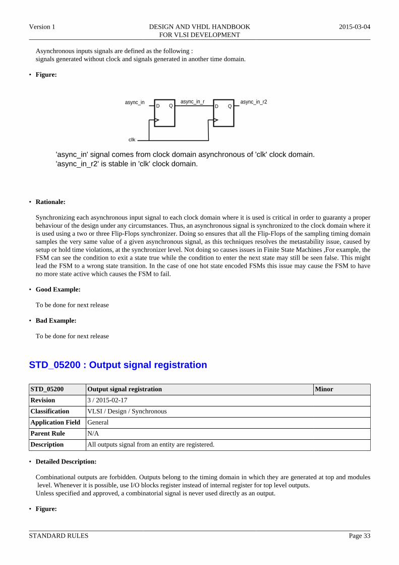
STD_05100 : Metastability management
STD_05100 Metastability management Major
Revision 3 / 2015-02-17
Classification VLSI / Design / Synchronous
Application Field General
Parent Rule N/A
Description Asynchronous input signals are synchronized with at least a two Flip-Flops synchronizer.
• Detailed Description:
Version 1 DESIGN AND VHDL HANDBOOKFOR VLSI DEVELOPMENT
2015-03-04
STANDARD RULES Page 33
Asynchronous inputs signals are defined as the following : signals generated without clock and signals generated in another time domain.
• Figure:
D D QQ
clk
async_in async_in_r async_in_r2
'async_in' signal comes from clock domain asynchronous of 'clk' clock domain.'async_in_r2' is stable in 'clk' clock domain.
• Rationale:
Synchronizing each asynchronous input signal to each clock domain where it is used is critical in order to guaranty a properbehaviour of the design under any circumstances. Thus, an asynchronous signal is synchronized to the clock domain where itis used using a two or three Flip-Flops synchronizer. Doing so ensures that all the Flip-Flops of the sampling timing domainsamples the very same value of a given asynchronous signal, as this techniques resolves the metastability issue, caused bysetup or hold time violations, at the synchronizer level. Not doing so causes issues in Finite State Machines ,For example, theFSM can see the condition to exit a state true while the condition to enter the next state may still be seen false. This mightlead the FSM to a wrong state transition. In the case of one hot state encoded FSMs this issue may cause the FSM to haveno more state active which causes the FSM to fail.
• Good Example:
To be done for next release
• Bad Example:
To be done for next release
STD_05200 : Output signal registration
STD_05200 Output signal registration Minor
Revision 3 / 2015-02-17
Classification VLSI / Design / Synchronous
Application Field General
Parent Rule N/A
Description All outputs signal from an entity are registered.
• Detailed Description:
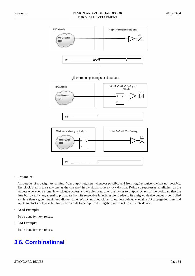
Combinational outputs are forbidden. Outputs belong to the timing domain in which they are generated at top and modules level. Whenever it is possible, use I/O blocks register instead of internal register for top level outputs.Unless specified and approved, a combinatorial signal is never used directly as an output.
• Figure:
Version 1 DESIGN AND VHDL HANDBOOKFOR VLSI DEVELOPMENT
2015-03-04
STANDARD RULES Page 34
output PAD with I/O flip flop and I/O buffer
combinatoriallogic
out
D Q
FPGA Matrix
out
glitch free outputs:register all outputs
output PAD with I/O buffer only
combinatoriallogic
out
FPGA Matrix
output PAD with I/O buffer only
combinatoriallogic
out
D Q
FPGA Matrix following by flip-flop
out
out
• Rationale:
All outputs of a design are coming from output registers whenever possible and from regular registers when not possible.The clock used is the same one as the one used in the signal source clock domain. Doing so suppresses all glitches on theoutputs whenever a signal level change occurs and enables control of the clocks to outputs delays of the design so that thetime borrowed by any signal to propagate from its respective launching clock edge to its assigned device output is controlledand less than a given maximum allowed time. With controlled clocks to outputs delays, enough PCB propagation time andinputs to clocks delays is left for those outputs to be captured using the same clock in a remote device.
• Good Example:
To be done for next release
• Bad Example:
To be done for next release
3.6. Combinational

Version 1 DESIGN AND VHDL HANDBOOKFOR VLSI DEVELOPMENT
2015-03-04
STANDARD RULES Page 35
STD_05300 : Sensitivity list for combinational processes
STD_05300 Sensitivity list for combinational processes Major
Revision 3 / 2015-02-17
Classification VLSI / Design / Combinational
Application Field General
Parent Rule N/A
Description Combinational processes have a sensitivity list including all inputs signals which are read.
• Detailed Description:
No additional information.
• Figure:
1
00
1
Process with incomplete sensibility list
s
a
b
P_mux2 : process(s) begin if (s = '1') then out <= b; else out <= a; end if; end process;
out
P_mux2 : process(s, a, b) begin if (s = '1') then out <= b; else out <= a; end if; end process;
s
a
b
out
Process is evaluated whenever s changes and not evaluated when a or b change since a and b inputs are missing from the sensitivity list.
Synthesized logic
pre synthesis behavior post synthesis behavior
For pre and post synthesis behavior concistancy complete the sensitivitylist.
s
a
b
out
• Rationale:
Version 1 DESIGN AND VHDL HANDBOOKFOR VLSI DEVELOPMENT
2015-03-04
STANDARD RULES Page 36
If an input signal is missing in the sensitivity list, there might be a mismatch between VHDL simulation and the programmedFPGA matrix.
• Good Example:
To be done for next release
• Bad Example:
To be done for next release
STD_05400 : Unsuitability of internal tristate
STD_05400 Unsuitability of internal tristate Major
Revision 3 / 2015-02-17
Classification VLSI / Design / Combinational
Application Field General
Parent Rule N/A
Description Internal tri-states drivers are forbidden inside VLSI.
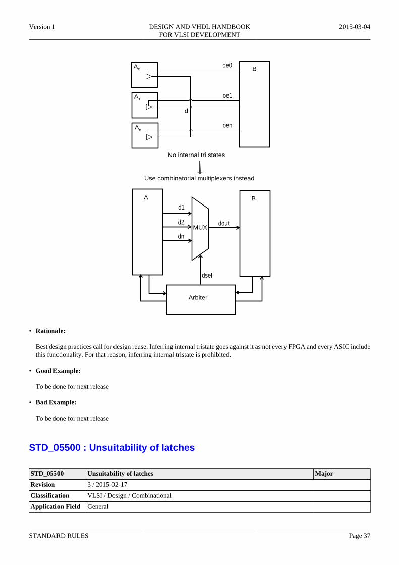
• Detailed Description:
When an internal tri-state solution would satisfy the functionality to model, use a multiplexer-based solution instead.Do not hesitate to pipeline the structure according to the targeted clock frequency and targeted technology.
• Figure:
Version 1 DESIGN AND VHDL HANDBOOKFOR VLSI DEVELOPMENT
2015-03-04
STANDARD RULES Page 37
A B
Arbiter
d1
d2
dn
dout
dsel
MUX
No internal tri states
Use combinatorial multiplexers instead
oe0
oe1
oen
A
A
A
0
1
n
B
d
• Rationale:
Best design practices call for design reuse. Inferring internal tristate goes against it as not every FPGA and every ASIC includethis functionality. For that reason, inferring internal tristate is prohibited.
• Good Example:
To be done for next release
• Bad Example:
To be done for next release
STD_05500 : Unsuitability of latches
STD_05500 Unsuitability of latches Major
Revision 3 / 2015-02-17
Classification VLSI / Design / Combinational
Application Field General
Version 1 DESIGN AND VHDL HANDBOOKFOR VLSI DEVELOPMENT
2015-03-04
STANDARD RULES Page 38
STD_05500 Unsuitability of latches Major
Parent Rule N/A
Description The design does not use latches on purpose.
• Detailed Description:
No additional information.
• Figure:

Version 1 DESIGN AND VHDL HANDBOOKFOR VLSI DEVELOPMENT
2015-03-04
STANDARD RULES Page 39
Using of latches:
D Q D DQ Q
clk
E
din dout
clk
di do
din
di
do
dout
FF1 FF2LATCH1
If t_comb < 1/2 clk period, din changes are seen on dout after 2 clk periods:
If t_comb > 1/2 clk period, din changes are seen on dout after 3 clk periods:
clk
din
di
do
dout
t_comb
No predictable behaviour. For it, use D-flip-flop instead.
Using of D flip-flop:
D Q D DQ Q
clk
din doutdi doFF1 FF2FF3
t_comb
2 clk periods 3 clk periods
clk
din
di
do
dout
3 clk periods regardless to t_comb
• Rationale:
Inferring latches in synchronous designs is not a good design practice. Even though a behavioural simulation shows that thedesign simulates correctly, it is only after a great deal of effort in synthesis place and route and static timing analysis and evenback annotated simulations that the design executes correctly on the targeted technology. This is because of the clock andsignals timing delays which very easily lead to a data crossing two latches at once when only one at once is desired.
Version 1 DESIGN AND VHDL HANDBOOKFOR VLSI DEVELOPMENT
2015-03-04
STANDARD RULES Page 40
• Good Example:
To be done for next release
• Bad Example:
To be done for next release
STD_05600 : Unsuitability of combinational feedbacks
STD_05600 Unsuitability of combinational feedbacks Major
Revision 3 / 2015-02-17
Classification VLSI / Design / Combinational
Application Field General
Parent Rule N/A
Description The design does not use combinatorial feedback.
• Detailed Description:
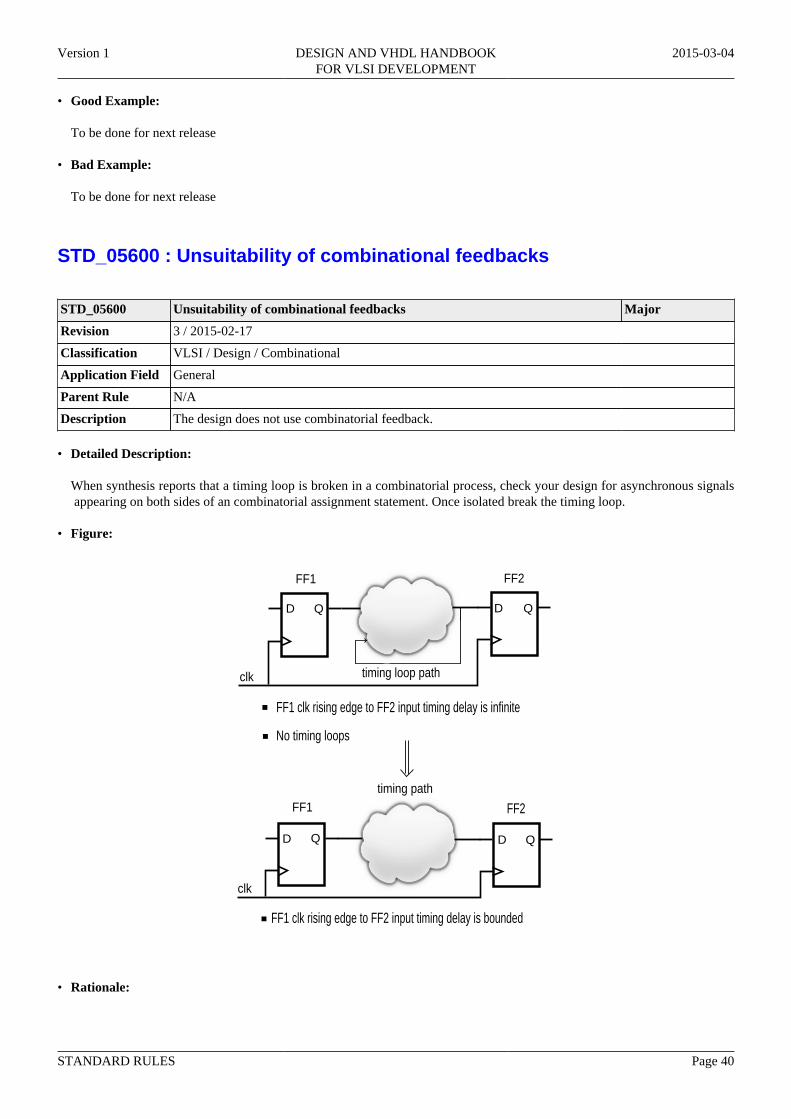
When synthesis reports that a timing loop is broken in a combinatorial process, check your design for asynchronous signals appearing on both sides of an combinatorial assignment statement. Once isolated break the timing loop.
• Figure:
D Q D Q
FF1 FF2timing path
FF1 clk rising edge to FF2 input timing delay is bounded
FF1 clk rising edge to FF2 input timing delay is infinite
No timing loops
FF1 FF2
D Q D Q
timing loop path
clk
clk
• Rationale:

Version 1 DESIGN AND VHDL HANDBOOKFOR VLSI DEVELOPMENT
2015-03-04
STANDARD RULES Page 41
Inferring Combinatorial feedbacks is not a good design practice. Even though a behavioural simulation shows that the designsimulates correctly, there is no guaranty that the design works properly on the targeted component. Indeed, every step of theway through the backend steps the timing loops provoked by these combinatorial feedbacks are broken so that the tool canproceed further. With doing so, all of the timing arcs proceed further. With doing so, all of the timing arcs passing throughthose combinatorial feedbacks are not analysed, leaving room for all sorts of timing violations thus a non working component.
• Good Example:
To be done for next release
• Bad Example:
To be done for next release
STD_05700 : Unsuitability of gated clocks
STD_05700 Unsuitability of gated clocks Major
Revision 3 / 2015-02-17
Classification FPGA / Design / Combinational
Application Field General
Parent Rule N/A
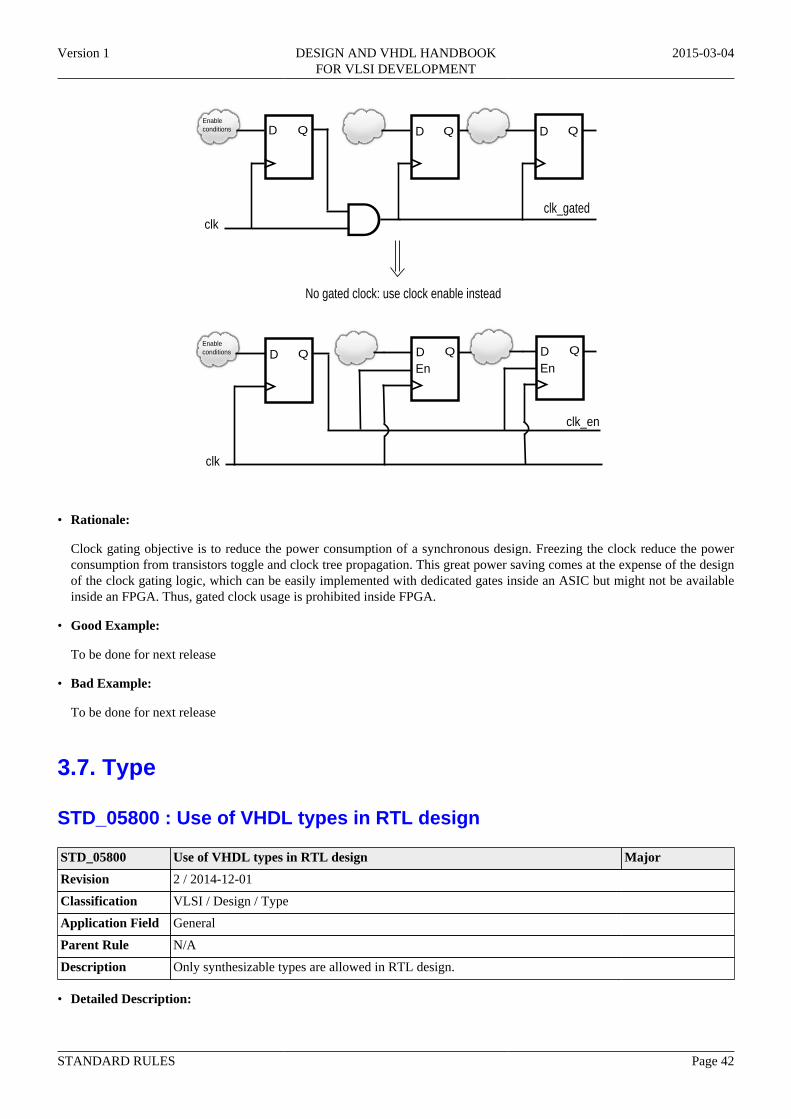
Description The design does not use gated clock.
• Detailed Description:
Intentionally inferring gated clock in FPGA is prohibited; use the Flip-Flops clock enable instead.When the synthesis reports that a gated clock was created, turn off the synthesis tool "auto convert gated clock" option. So that the tool uses the Flip-Flops clock enable instead.
• Figure:
Version 1 DESIGN AND VHDL HANDBOOKFOR VLSI DEVELOPMENT
2015-03-04
STANDARD RULES Page 42
No gated clock: use clock enable instead
D Q D DQ QEnableconditions
clk_gatedclk
Q Q Q
EnEn
Enableconditions
clk
clk_en
D DD
• Rationale:
Clock gating objective is to reduce the power consumption of a synchronous design. Freezing the clock reduce the powerconsumption from transistors toggle and clock tree propagation. This great power saving comes at the expense of the designof the clock gating logic, which can be easily implemented with dedicated gates inside an ASIC but might not be availableinside an FPGA. Thus, gated clock usage is prohibited inside FPGA.
• Good Example:
To be done for next release
• Bad Example:
To be done for next release
3.7. Type
STD_05800 : Use of VHDL types in RTL design
STD_05800 Use of VHDL types in RTL design Major
Revision 2 / 2014-12-01
Classification VLSI / Design / Type
Application Field General
Parent Rule N/A
Description Only synthesizable types are allowed in RTL design.
• Detailed Description:
Version 1 DESIGN AND VHDL HANDBOOKFOR VLSI DEVELOPMENT
2015-03-04
STANDARD RULES Page 43
Only the following types are allowed for RTL design : std_logic, std_logic_vector, integer, signed, unsigned and record/array of those.Enumerate is allowed for FSMs and boolean for generics.
• Rationale:
VHDL language provides many different types. These types have not got any physical match inside a physical componentbut are only used for simulation purpose.
• Good Example:
To be done for next release
• Bad Example:
To be done for next release
STD_05900 : Range for integers
STD_05900 Range for integers Major
Revision 2 / 2014-12-01
Classification VLSI / Design / Type
Application Field General
Parent Rule N/A
Description Integer type are constrained using the keyword "range".
• Detailed Description:
No additional information.
• Rationale:
Usage of "range" keyword constraints synthesis optimization effort. It avoids mismatches between simulation and board.
• Good Example:
To be done for next release
• Bad Example:
To be done for next release
STD_06000 : Range direction for arrays
STD_06000 Range direction for arrays Major
Revision 2 / 2014-12-01
Classification VLSI / Design / Type
Application Field General
Parent Rule N/A
Description "Array" type declaration uses increasing index with "to" keyword.
• Detailed Description:
Version 1 DESIGN AND VHDL HANDBOOKFOR VLSI DEVELOPMENT
2015-03-04
STANDARD RULES Page 44
No additional information.
• Rationale:
This is an convention to improve use of arrays.
• Good Example:
To be done for next release
• Bad Example:
To be done for next release
STD_06100 : Range direction for std_logic_vector
STD_06100 Range direction for std_logic_vector Minor
Revision 3 / 2015-02-17
Classification VLSI / Design / Type
Application Field General
Parent Rule N/A
Description "Std_logic_vector" type declaration uses decreasing index with "downto" keyword.
• Detailed Description:
No additional information.
• Rationale:
This is an convention to improve use of std_logic_vector.
• Good Example:
To be done for next release
• Bad Example:
To be done for next release
STD_06200 : Management of numeric values
STD_06200 Management of numeric values Minor
Revision 2 / 2014-12-01
Classification VLSI / Design / Type
Application Field General
Parent Rule N/A
Description Use VHDL constant as much as possible instead of hard coded numeric values.
• Detailed Description:
No additional information.
• Rationale:

Version 1 DESIGN AND VHDL HANDBOOKFOR VLSI DEVELOPMENT
2015-03-04
STANDARD RULES Page 45
Using constant instead of hard coded numeric value inside the VHDL improve the identification of these value. Thus,modification of these values (if needed) will be easier.
• Good Example:
To be done for next release
• Bad Example:
To be done for next release
STD_06300 : Unsuitability of variables in RTL design
STD_06300 Unsuitability of variables in RTL design Minor
Revision 2 / 2014-12-01
Classification VLSI / Design / Type
Application Field General
Parent Rule N/A
Description Variables are prohibited in the RTL design.
• Detailed Description:
Only signal type is allowed in RTL design.
• Rationale:
VHDL signal is the object used to describe a electrical wire connection or a register. VHDL signal is the way to have acommunication between VHDL processes. Whereas variable is restricted inside a VHDL process. Its physical implementationdepends on the way of using it. Using variable can lead to simulation and synthesis mismatch.
• Good Example:
To be done for next release
• Bad Example:
To be done for next release
3.8. Reliability
STD_06400 : Error mitigation strategy
STD_06400 Error mitigation strategy Major
Revision 2 / 2014-12-01
Classification VLSI / Design / Reliability
Application Field Spatial
Parent Rule N/A
Description All mitigation mechanisms are done with a specific approved mechanism.
• Detailed Description:
Version 1 DESIGN AND VHDL HANDBOOKFOR VLSI DEVELOPMENT
2015-03-04
STANDARD RULES Page 46
In order to mitigate errors due to radiation, mechanisms(EDAC,ECC,parity,srubbing,triplication...) can be implemented in the FPGA if needed.
• Rationale:
Error mitigation can be made at VHDL design level. If it is expected to be done at this level, the mechanisms have to beapproved.
STD_06500 : Counters end of counting
STD_06500 Counters end of counting Minor
Revision 2 / 2014-12-01
Classification VLSI / Design / Reliability
Application Field General
Parent Rule STD_06400
Description Use non strict comparison (<= and >=) for end of counting comparison.
• Detailed Description:
When comparing a cyclic counter value against its end of count value, non strict comparison is used instead of strict comparison.For an up counter, use the greater than or equal to (>=) comparison sign instead of the equals sign (=).For a down counter, use the less than or equal (<=) comparison sign instead of the equals sign (=).
• Rationale:
This feature allows the synthesizer to optimize the counter in a way that if the counted value pass over the final one the endof counter is still reached. The result of the synthesis can sometimes be more efficient than with the use of "=".
• Good Example:
To be done fort next release
• Bad Example:
To be done fort next release
STD_06600 : Dimension of comparison elements
STD_06600 Dimension of comparison elements Minor
Revision 1 / 2015-02-17
Classification VLSI / Design / Reliability
Application Field General
Parent Rule N/A
Description Two comparison elements must have the same type and dimension.
• Detailed Description:
Using of unsigned or signed type to insure comparison between two elements is a best practice.
• Rationale:
Version 1 DESIGN AND VHDL HANDBOOKFOR VLSI DEVELOPMENT
2015-03-04
STANDARD RULES Page 47
Comparison of two std_logic_vector signal of different size can lead to unexpected result.
• Good Example:
To be done for next release
• Bad Example:
To be done for next release
3.9. Miscellaneous
STD_06700 : Unsuitability of wait statement in RTL design
STD_06700 Unsuitability of wait statement in RTL design Major
Revision 3 / 2015-02-17
Classification VLSI / Design / Miscellaneous
Application Field General
Parent Rule N/A
Description The "wait" statement and "after" clause are forbidden in RTL design.
• Detailed Description:
No additional information.
• Rationale:
"Wait" instructions and "after" clauses are forbidden inside the RTL design because they are not synthesizable.
• Good Example:
To be done for next release
• Bad Example:
To be done for next release
STD_06800 : Unsuitability of signal initialization in declaration section
STD_06800 Unsuitability of signal initialization in declaration section Major
Revision 2 / 2014-12-01
Classification VLSI / Design / Miscellaneous
Application Field General
Parent Rule N/A
Description Signals are never initialized to a default value when declared.
• Detailed Description:
Signals are not initialized to a default value in declaration level but only during a reset sequence.
• Rationale:
Version 1 DESIGN AND VHDL HANDBOOKFOR VLSI DEVELOPMENT
2015-03-04
STANDARD RULES Page 48
Signals default value, in declaration section, is usually not synthesizable.
• Good Example:
To be done for next release
• Bad Example:
To be done for next release
STD_06900 : Unsuitability of procedures and functions in RTL design
STD_06900 Unsuitability of procedures and functions in RTL design Minor
Revision 2 / 2014-12-01
Classification VLSI / Design / Miscellaneous
Application Field General
Parent Rule N/A
Description Procedures and functions are forbidden in RTL design.
• Detailed Description:
No additional information.
• Rationale:
VHDL provide synthesizable object (Process and Component) to structure and replicate statements. Procedures and functionsare not provided for synthesis approach but for testbench development.
STD_07000 : Maximum depths of nested objects
STD_07000 Maximum depths of nested objects Minor
Revision 1 / 2015-02-17
Classification VLSI / Design / Miscellaneous
Application Field General
Parent Rule N/A
Description Nested VHDL objects are limited in depth.
• Detailed Description:
The depth of nested objects (entities, packages, dimensions) should be kept limited.
• Rationale:
Nested objects limited in depth improves understanding of project and keep modules less complicated.

Version 1 DESIGN AND VHDL HANDBOOKFOR VLSI DEVELOPMENT
2015-03-04
STANDARD RULES Page 49
4. Simulation
4.1. Miscellaneous
STD_07100 : Simulation ending
STD_07100 Simulation ending Major
Revision 2 / 2014-12-01
Classification VLSI / Simulation / Miscellaneous
Application Field General
Parent Rule N/A
Description The simulation duration is terminated by an automatic mechanism.
• Detailed Description:
The simulation stop automatically without any human action in the simulator. This can be done by external scripts, event starvations (like freezing the main clocks) in the testbench.
• Rationale:
Limited duration for testbenches avoid useless simulation runs (beyond stimulus range) thus free machine resources for otherdesigners. This allows the automatic sequencing of testbenches (during non regression test for instance).
• Good Example:
To be done for next release
• Bad Example:
To be done for next release
STD_07200 : Use of procedures and functions in testbenches
STD_07200 Use of procedures and functions in testbenches Minor
Revision 2 / 2014-12-01
Classification VLSI / Simulation / Miscellaneous
Application Field General
Parent Rule N/A
Description Procedures and functions are recommended in testbenches.
• Detailed Description:
No additional information.
• Rationale:
Testbench are not made to be synthesized. Thus, VHDL not synthesizable features can be used inside testbenches. Functionsand procedures in testbenches ensure saving time of development. Moreover, the testbench is more compact because identicalinstructions aren't repeated which ensures better understanding and reduce the error number.
Version 1 DESIGN AND VHDL HANDBOOKFOR VLSI DEVELOPMENT
2015-03-04
STANDARD RULES Page 50
STD_07300 : Use of wait statement in testbenches
STD_07300 Use of wait statement in testbenches Minor
Revision 3 / 2015-02-17
Classification VLSI / Simulation / Miscellaneous
Application Field General
Parent Rule N/A
Description Testbench are scheduled with "wait" instruction and "after" clause instead of combinational process.
• Detailed Description:
No additional information.
• Rationale:
Use of wait statement or "after" clause allows designer to not maintain a process sensitivity list while developing a testbench(sensitivity list is empty when a wait is used inside a process). The testbench instruction inside a process is then sequentialwhich is coherent with most testbench stimulation sequences.
• Good Example:
To be done for next release
• Bad Example:
To be done for next release