Embed Size (px)
Citation preview
Design and Implementation of a Re-configurable
Arbitrary Signal Generator and Radio Frequency
Spectrum Analyser
A thesis submitted in partial fulfilment of the requirements of
the University of Hertfordshire for the degree of Doctor of
Philosophy
Ashok Kumar Sharma
Supervisor: Professor Yichuang Sun
November 2015
Confidential and commercially sensitive
Embargo on public availability of information contained in
this thesis for 2 years


Abstract iii
Design and implementation of a re-configurable arbitrary signal generator and radio frequency spectrum analyser
Abstract
This research is focused on the design, simulation and implementation of a
reconfigurable arbitrary signal generator and the design, simulation and
implementation of a radio frequency spectrum analyser based on digital signal
processing.
Until recently, Application Specific Integrated Circuits (ASICs) were used to produce
high performance re-configurable function and arbitrary waveform generators with
comprehensive modulation capabilities. However, that situation is now changing with
the availability of advanced but low cost Field Programmable Gate Arrays (FPGAs),
which could be used as an alternative to ASICs in these applications. The availability
of high performance FPGA families opens up the opportunity to compete with ASIC
solutions at a fraction of the development cost of an ASIC solution. A fast digital
signal processing algorithm for digital waveform generation, using primarily but not
limited to Direct Digital Synthesis (DDS) technologies, developed and implemented in
a field-configurable logic, with control provided by an embedded microprocessor
replacing a high cost ASIC design appeared to be a very attractive concept. This
research demonstrates that such a concept is feasible in its entirety.
A fully functional, low-complexity, low cost, pulse, Gaussian white noise and DDS
based function and arbitrary waveform generator, capable of being amplitude,
frequency and phase modulated by an internally generated or external modulating
signal was implemented in a low-cost FPGA. The FPGA also included the
capabilities to perform pulse width modulation and pulse delay modulation on pulse
waveforms. Algorithms to up-convert the sampling rate of the external modulating
signal using Cascaded Integrator Comb (CIC) filters and using interpolation method
were analysed. Both solutions were implemented to compare their hardware
complexities. Analysis of generating noise with user-defined distribution is presented.
The ability of triggering the generator by an internally generated or an external event
to generate a burst of waveforms where the time between the trigger signal and
waveform output is fixed was also implemented in the FPGA. Finally, design of
interface to a microprocessor to provide control of the versatile waveform generator
was also included in the FPGA. This thesis summarises the literature, design
considerations, simulation and implementation of the generator design.
Abstract iv
Design and implementation of a re-configurable arbitrary signal generator and radio frequency spectrum analyser
The second part of the research is focused on radio frequency spectrum analysis
based on digital signal processing. Most existing spectrum analysers are analogue in
nature and their complexity increases with frequency. Therefore, the possibility of
using digital techniques for spectrum analysis was considered. The aim was to come
up with digital system architecture for spectrum analysis and to develop and
implement the new approach on a suitable digital platform.
This thesis analyses the current literature on shifting algorithms to remove spurious
responses and highlights its drawbacks. This thesis also analyses existing literature
on quadrature receivers and presents novel adaptation of the existing architectures
for application in spectrum analysis. A wide band spectrum analyser receiver with
compensation for gain and phase imbalances in the Radio Frequency (RF) input
range, as well as compensation for gain and phase imbalances within the
Intermediate Frequency (IF) pass band complete with Resolution Band Width (RBW)
filtering, Video Band Width (VBW) filtering and amplitude detection was implemented
in a low cost FPGA. The ability to extract the modulating signal from a frequency or
amplitude modulated RF signal was also implemented. The same family of FPGA
used in the generator design was chosen to be the digital platform for this design.
This research makes arguments for the new architecture and then summarises the
literature, design considerations, simulation and implementation of the new digital
algorithm for the radio frequency spectrum analyser.

Acknowledgements v
Design and implementation of a re-configurable arbitrary signal generator and radio frequency spectrum analyser
Acknowledgements
My research would not have been possible without the support of many family,
friends and colleagues.
In particular I would like to thank Professor Yichuang Sun for his invaluable guidance,
help, support, motivation and understanding, particularly through many difficult
personal times that I have experienced over the past few years. It has truly been an
honour to work with Professor Sun on this project.
I would also like to acknowledge the support and contribution of the following people.
I thank you for your time and effort throughout the duration of my research.
Dr David Lauder School of Engineering and Technology, University of
Hertfordshire (Secondary Supervisor)
Dr Faycal Bensaali School of Engineering and Technology, University of
Hertfordshire (Secondary Supervisor)
Mr. Chris Wilding Thurlby Thandar Instruments Limited (Secondary
Supervisor)
Mr. Roy Willis Thurlby Thandar Instruments Limited
Mr. John Tothill Thurlby Thandar Instruments Limited
Mr. Mick Whittaker Thurlby Thandar Instruments Limited
Mr. Shiv Mahadevappa Thurlby Thandar Instruments Limited
Mr. Richard Laver Waterbeach Electronics Limited
Last but not least, I would like to thank my wife Priya for her love and support and my
daughters Shreya and Parul for putting up with my frequent absences while I was
engaged in this research. I am grateful to you all.

Declaration vi
Design and implementation of a re-configurable arbitrary signal generator and radio frequency spectrum analyser
Declaration
I certify that the work submitted is my own and that any material derived or quoted
from the published or unpublished work of other persons has been duly
acknowledged.
The research work was carried out for Thurlby Thandar Instruments Limited in
collaboration with the University of Hertfordshire within the Knowledge Transfer
Partnership (KTP) scheme. This PhD thesis includes design and implementation
work of two KTP projects concerning arbitrary signal generators and radio frequency
spectrum analysers respectively and contains commercially sensitive information.
Student Full Name: Ashok Kumar Sharma
Student Registration Number: 07166544
Signed: ………………………………...
Date: …………………………………...

Contents vii
Design and implementation of a re-configurable arbitrary signal generator and radio frequency spectrum analyser
Contents Abstract iii Acknowledgements v Declaration vi Contents vii List of Abbreviations xi List of Figures xiii List of Tables xviii 1 Introduction 1
1.1 Background 2 1.1.1 Direct Digital Synthesis 2 1.1.2 Image Rejection in Spectrum Analysers 3 1.2 Research Scope and Objectives 5 1.3 Original Contributions 6 1.4 Structure of Thesis 6
2 Re-Configurable Arbitrary Waveform Function Generators 8 2.1 Introduction 8 2.2 Direct Digital Synthesis 8 2.3 DDS Modulation Capability 10 2.4 DDS Trigger Uncertainty 12 2.5 DDS Modulation Using an External Signal 14 2.6 Arbitrary Waveform Generation 15 2.7 Pulse Generation 15 2.8 White Noise Generation 17 2.9 Simulation of DDS Systems 18 2.10 Simulation of Modulated DDS 29 2.11 Simulation of DDS Modulation Using an External Signal 44

Contents viii
Design and implementation of a re-configurable arbitrary signal generator and radio frequency spectrum analyser
2.12 Conclusion 48 3 Waveform Generator – FPGA Design Simulation and Synthesis 49 3.1 Introduction 49 3.2 Evaluation of FPGA Technologies 50 3.3 DDS Carrier Generator 51 3.4 DDS Modulation Generator 54 3.5 White Noise Generator 56 3.6 Pulse Generator 61 3.7 Arbitrary Waveform Generator 64 3.8 External Modulation 65 3.9 Trigger Uncertainty Compensation 67 3.10 FPGA Microprocessor Interface 71 3.11 FPGA Synthesis 74 3.12 Results 76 3.13 Conclusion 87 4 Digital Signal Processing Based Radio Frequency Spectrum Analysis 88 4.1 Introduction 88 4.2 Literature review of shifting algorithms 88 4.3 Quadrature image reject receiver architecture 90 4.4 IQ imbalance compensation literature review 91 4.5 IQ imbalance compensation within the IF pass-band 92 4.6 Modelling of IQ imbalance 93 4.7 Modelling of imbalance computation by correlation method 96 4.8 Modelling of Weaver architecture 97 4.9 Modelling of image rejection in Weaver architecture 101 4.10 Modelling of Weaver base-band architecture 102 4.11 Modelling of imbalance computation using Weaver base-band architecture 102

Contents ix
Design and implementation of a re-configurable arbitrary signal generator and radio frequency spectrum analyser
4.12 Simulation of imbalance computation by correlation method 104 4.13 Simulation of Weaver Architecture 114 4.14 Simulation of Weaver base-band architecture 120 4.15 Simulation of imbalance computation using Weaver base-band architecture 123 4.16 Simulation of IQ imbalance compensation within the IF pass-band 125 4.17 Conclusion 129 5 Spectrum Analyser – FPGA Design Simulation and Synthesis 130 5.1 Introduction 130 5.2 LVDS Receiver 131 5.3 IF pass-band imbalance compensation 133 5.4 RF imbalance compensation 134 5.5 Weaver mixers 136 5.6 Resolution bandwidth filters 138 5.7 Weaver adders 140 5.8 Amplitude detector 142 5.9 Video bandwidth filters 142 5.10 Demodulation 142 5.11 RF imbalance computation block 143 5.12 FPGA synthesis 146 5.13 Results 149 5.14 Conclusion 160 6 Conclusions and Future Work 161 References 165 Appendices 175 Appendix A: Comparison table of the waveform generator 175 Appendix B: Target specification of the waveform generator 186 Appendix C: Comparison table of the digital spectrum analyser 195
Contents x
Design and implementation of a re-configurable arbitrary signal generator and radio frequency spectrum analyser
Appendix D: Target specification of the spectrum analyser 208
List of Abbreviations xi
Design and implementation of a re-configurable arbitrary signal generator and radio frequency spectrum analyser
List of Abbreviations
ADC Analogue to Digital Converter AM Amplitude Modulation AS Active Serial ASIC Application Specific Integrated Circuit CIC Cascaded Integrator Comb CORDIC COordinate Rotation DIgital Computer DAC Digital to Analogue Converter DANL Displayed Average Noise Level DC Direct Current DCM Digital Clock Manager DDC Digital Down Conversion DDS Direct Digital Synthesis DSP Digital Signal Processing FCW Frequency Control Word FFT Fast Fourier Transform FIR Finite Impulse Response FM Frequency Modulation FPGA Field Programmable Gate Array FSK Frequency Shift Keying IF Intermediate Frequency IQ In-phase and Quadrature IRR Image Rejection Ratio JTAG Joint Test Action Group KTP Knowledge Transfer Partnership LAB Logic Array Block LCD Liquid Crystal Display
List of Abbreviations xii
Design and implementation of a re-configurable arbitrary signal generator and radio frequency spectrum analyser
LE Logic Element LFSR Linear Feedback Shift Register LO Local Oscillator LPF Low Pass Filters LSB Lower Side Band LVDS Low Voltage Differential Signal MSBs Most Significant Bits PCB Printed Circuit Board PLL Phase Lock Loop PM Phase Modulation PS Passive Serial QAM Quadrature Amplitude Modulation RAM Random Access Memory RBW Resolution Band Width RF Radio Frequency RMS Root Mean Square ROM Read Only Memory RTL Register Transfer Level SFDR Spurious Free Dynamic Range SPI Serial to Parallel Interface TFT Thin Film Transistor UART Universal Asynchronous Receiver Transmitter USB Universal Serial Bus USB Upper Side Band VBW Video Band Width VCO Voltage Controlled Oscillator VHDL Very High Speed Integrated Circuit (VHSIC) Hardware
Descriptive Language

List of Figures xiii
Design and implementation of a re-configurable arbitrary signal generator and radio frequency spectrum analyser
List of Figures
Figure 1.1. Simplified block diagram of a DDS 2 Figure 1.2. Block diagram of a classic super heterodyne spectrum analyser 3 Figure 1.3. Image rejection mixer 5 Figure 2.1. Block diagram of DDS phase accumulator 8 Figure 2.2. Block diagram of DDS phase to amplitude converter (RAM) 10 Figure 2.3. Simplified DDS architecture with modulation capability 11 Figure 2.4. Delay line for trigger uncertainty compensation 12 Figure 2.5. FPGA carry chain implemented as a delay line 13 Figure 2.6. Variable clock architecture for arbitrary waveform generator 15 Figure 2.7. PDF of the generated noise 18 Figure 2.8. Simulation of 16-bit un-modulated direct digital synthesis 19 Figure 2.9. Phase accumulator output 20 Figure 2.10. Phase to amplitude converter output in the time domain 22 Figure 2.11. Frequency spectrum of the DDS output where accumulator output is truncated to 10 bits 23 Figure 2.12. Frequency spectrum of the DDS output where accumulator output is not truncated 24 Figure 2.13. Simulation of 32-bit direct digital synthesis 26 Figure 2.14. Frequency spectrum for 16-bit output 27 Figure 2.15. Frequency spectrum for 14-bit output 28 Figure 2.16. Simulation of frequency modulation in a DDS system 30 Figure 2.17. Frequency spectrum of a frequency modulated DDS output 31 Figure 2.18. Simulation of phase modulation in a DDS system 33 Figure 2.19. Frequency spectrum of a phase modulated DDS output 34 Figure 2.20. Phase modulated waveform output in the time domain 35 Figure 2.21. Simulation of amplitude modulation in a DDS system 37 Figure 2.22. Frequency spectrum of an amplitude modulated DDS output (carrier is not suppressed) 38

List of Figures xiv
Design and implementation of a re-configurable arbitrary signal generator and radio frequency spectrum analyser
Figure 2.23. Modulation waveform and amplitude modulated carrier in the time domain 39 Figure 2.24. Simulation of suppressed carrier amplitude modulation in a DDS system 41 Figure 2.25. Frequency spectrum of an amplitude modulated DDS output (carrier is suppressed) 42 Figure 2.26. Suppressed carrier amplitude modulation in the time domain 43 Figure 2.27. Simulation of sample rate conversion using interpolation method 44 Figure 2.28. Frequency spectrum of interpolated waveform output 45 Figure 2.29. Simulation of sample rate conversion using CIC filter 46 Figure 2.30. Frequency spectrum of CIC filter output 47 Figure 3.1. FPGA block diagram - input/output connections 49 Figure 3.2. RTL view of the carrier generator 52 Figure 3.3. FPGA DAC connections 54 Figure 3.4. RTL view of the modulation generator 55 Figure 3.5. Block diagram of white noise generator 58 Figure 3.6. RTL view of the noise generator 60 Figure 3.7. RTL view of the pulse generator 62 Figure 3.8. Effect of sampling on edge detection 64 Figure 3.9. RTL view of the CIC filter 66 Figure 3.10. RTL view of the trigger uncertainty compensation block 68 Figure 3.11. Trigger delay line placement in the FPGA 70 Figure 3.12. FPGA microprocessor interface 71 Figure 3.13. RTL view of the overall waveform generator 73 Figure 3.14. FPGA pin assignment – top level view 75 Figure 3.15. Waveform generator prototype board 76 Figure 3.16. Simulation results for the carrier phase accumulator 78 Figure 3.17. Simulation results for white noise generator 79 Figure 3.18. Simulation results for pulse generator 80
List of Figures xv
Design and implementation of a re-configurable arbitrary signal generator and radio frequency spectrum analyser
Figure 3.19. Spectrum of a 25.01 MHz un-modulated DDS sine waveform 81 Figure 3.20. Scope measurement - DDS sine 82 Figure 3.21. Scope measurement - DDS pulse 82 Figure 3.22. Scope measurement – DDS sinc 83 Figure 3.23. Scope measurement - DDS cardiac 83 Figure 3.24. Scope measurement – amplitude modulation 84 Figure 3.25. Scope measurement – suppressed carrier amplitude modulation 84 Figure 3.26. Scope measurement – frequency modulation 85 Figure 3.27. Scope measurement – phase modulation 85 Figure 3.28. Scope measurement – frequency shift keying 86 Figure 3.29. Scope measurement – pulse width modulation 86 Figure 3.30. Scope measurement – triggered pulse 87 Figure 3.31. Scope measurement – white noise 87 Figure 4.1. Block diagram of the initially proposed RF architecture 88 Figure 4.2. Block diagram of the revised RF architecture 90 Figure 4.3. Quadrature frequency down conversion model 93 Figure 4.4. Quadrature frequency down conversion model with all gain/phase imbalances placed in the Q channel 94 Figure 4.5. Compensation model for gain and phase imbalances 95 Figure 4.6. Block diagram of the Weaver architecture 97 Figure 4.7. Block diagram of the Weaver base-band architecture 102 Figure 4.8. Imbalance computation method using Weaver base-band architecture 104 Figure 4.9. Simulation of imbalance computation by correlation method 106 Figure 4.10. Simulation of error detection block with phase noise 108 Figure 4.11. Simulation of error detection block with uncorrelated noise 110 Figure 4.12. Error detection block with multiplying factors as output 112 Figure 4.13. Error compensation block 113 Figure 4.14. Simulation of Weaver Architecture 115

List of Figures xvi
Design and implementation of a re-configurable arbitrary signal generator and radio frequency spectrum analyser
Figure 4.15. 25 MHz signals sampled at 100 MHz 116 Figure 4.16. Magnitude response of the filters in the Weaver architecture 117 Figure 4.17. Output waveforms without gain or phase error 118 Figure 4.18. Output waveforms (gain error 2 %, phase error 0.1 radians) 119 Figure 4.19. Simulation of Weaver base-band architecture 121 Figure 4.20. Magnitude response of the resolution bandwidth filters 122 Figure 4.21. Wanted and image outputs 123 Figure 4.22. Simulation of imbalance computation using Weaver base-band architecture 124 Figure 4.23. Magnitude response of the FIR filter 127 Figure 4.24. Phase response of the FIR filter 128 Figure 5.1. Analogue section of the RF architecture 130 Figure 5.2. RTL view of the LVDS receiver 132 Figure 5.3. RTL view of the LVDS decoder 133 Figure 5.4. Direct form realisation of FIR filter 133 Figure 5.5. RTL view of RF imbalance compensation 135 Figure 5.6. RTL view of Weaver mixers 137 Figure 5.7. RTL view of RBW filters 138 Figure 5.8. Realisation of a symmetric FIR filter 139 Figure 5.9. Magnitude response of the RBW FIR filter 140 Figure 5.10. RTL view of the Weaver adders 141 Figure 5.11. RTL view of the imbalance computation block 145 Figure 5.12. FPGA pin assignment – top level view 147 Figure 5.13 FPGA ADC connections 148 Figure 5.14. Spectrum analyser prototype board 148 Figure 5.15. Spectrum of 1 GHz signal input 150 Figure 5.16. Spectrum of 1 GHz signal input for wide RBW setting 151 Figure 5.17. Spectrum of 1 GHz signal input for narrow RBW setting 152
List of Figures xvii
Design and implementation of a re-configurable arbitrary signal generator and radio frequency spectrum analyser
Figure 5.18. Spectrum of 1 GHz signal input for narrow VBW setting 153 Figure 5.19. Spectrum of FM modulated 1 GHz signal input 154 Figure 5.20. FM Demodulated waveform 155 Figure 5.21. AM Demodulated waveform 156 Figure 5.22. Image rejection when compensation is not applied 157 Figure 5.23. Image rejection when compensation is applied 158 Figure 5.24. Image rejection when IF pass-band compensation is not applied 159 Figure 5.25. Image rejection when IF pass-band compensation is applied 160

List of Tables xviii
Design and implementation of a re-configurable arbitrary signal generator and radio frequency spectrum analyser
List of Tables
Table 3.1. Comparison of FPGAs 50 Table 3.2. LFSR configurations in the white noise generator 57 Table 3.3. Quartus flow summary for the generator project 74 Table 4.1. Measured gain and phase imbalance across IF pass-band 125 Table 5.1. RBW filters – decimation rate and CIC bit growth 139 Table 5.2. Quartus flow summary for the spectrum analyser project 146 Table 8.1 Comparison of function arbitrary waveform generators 185 Table 8.2 Comparison of 6 GHz hand-held radio frequency spectrum analysers 207

Introduction 1
Design and implementation of a re-configurable arbitrary signal generator and radio frequency spectrum analyser
1 Introduction
Thurlby Thandar Instruments is a leading manufacturer of electronic test and
measurement instruments. The aim and key objectives of this research was to
replace the company’s existing low cost waveform generator and radio frequency
spectrum analyser with a generator and a spectrum analyser which matches or
exceeds the specifications of the company’s benchmark competitors. Comparison
tables were prepared to analyse and compare the features and benefits of the
existing products against market competition and subsequently target specifications
were prepared for the new products. For the comparison table and target
specification of the waveform generator, refer to Appendix A and Appendix B
respectively. For the comparison table and target specification of the radio frequency
spectrum analyser, refer to Appendix C and Appendix D respectively.
It was evident that the new 50 MHz generator based on the principles of DDS will
have to have comprehensive modulation capabilities together with the ability of
generating waveforms not based on DDS to be competitive in the market. It was also
quite clear from the comparison table that the existing spectrum analysers
manufactured by the company although significantly cheaper than comparable
competitors’ products and with decent Spurious Free Dynamic Range (SFDR) of
60 dB, Displayed Average Noise Level (DANL) of -96 dBm with reference level of
-20 dBm and Resolution Bandwidth of 15 kHz and phase noise performance of
-90 dBc/Hz at carrier frequency of 500 MHz and 100 kHz offset, lacked many
features and capabilities. It was concluded that the new product would have to meet
many key requirements on top of the current performance in order to be competitive
in the market.
The architectures of the existing spectrum analysers were entirely analogue up to
and including the detectors. Initial work on the architecture needed to extend the
frequency range with sufficient performance showed it to be highly complex in
analogue terms. The existing architecture would have required the Local Oscillator
(LO) to generate frequencies much higher than 6 GHz. This is very difficult to
implement in a transistor based Voltage Controlled Oscillator (VCO) design.
Therefore, the possibility of using digital techniques was considered and it was the
requirement of this project to carry out detailed theoretical analysis of the digital

Introduction 2
Design and implementation of a re-configurable arbitrary signal generator and radio frequency spectrum analyser
techniques for implementing spectrum analysers. This is summarised in this thesis.
The aim of this analysis was to come up with a proposed RF and digital system
architecture and to make recommendations on the direction of progress and
ultimately to develop and implement the agreed approach on a suitable digital
platform.
This chapter contains a brief introduction of direct digital synthesis and the reasons
for choosing digital spectrum analysis techniques followed by a description of the key
aspects of the project.
1.1 Background
1.1.1 Direct Digital Synthesis
DDS first proposed by Tierney et al in 1976 is a popular method that is used to
generate waveforms of any shape that has a linear and periodic phase [1]. Figure 1.1
below is a simplified block diagram of a DDS architecture. FCW is the frequency
control word input to the phase accumulator. The frequency, amplitude and phase of
waveforms generated using DDS can be precisely controlled since it is essentially a
digital system [2]. It is also possible to achieve very high frequency resolution and
fast frequency switching using DDS. It is very easy to introduce modulation in DDS
because the signal is in digital form [3].
DDS is fast replacing traditional analogue circuit functions. With recent performance
and complexity increases in FPGA and microprocessor technologies, a low cost user
configurable waveform generator based on DDS can be efficiently realised.
Figure 1.1. Simplified block diagram of a DDS
FCW WAVEFORM

Introduction 3
Design and implementation of a re-configurable arbitrary signal generator and radio frequency spectrum analyser
The advantages of using FPGAs as opposed to ASICs are very obvious. Designs
implemented in a FPGA are less risky as they can easily be re-configured and the
design cycle is much smaller compared to other types of semiconductors. FPGAs
configure themselves upon every power up and therefore, changes in the design can
simply be made by downloading a new configuration into the device. Competing
ASICs have fixed functionality that can’t be changed without great cost and time [4].
Very high-speed integrated circuits Hardware Description Language (VHDL) was
predominantly used to model the signal generator system which makes the design
even more versatile as it can be easily moved to any new FPGA platform.
This thesis charts the development of a versatile user re-configurable waveform
generator, primarily based on but not limited to direct digital synthesis with
comprehensive modulation capabilities built on a configurable logic.
1.1.2 Image Rejection in Spectrum Analysers
The main challenge presented in the development of the spectrum analyser was to
remove images associated with the down conversion of RF input frequency to some
intermediate frequency for further processing. Most existing spectrum analysers are
based on conventional super heterodyne architecture as shown in Figure 1.2 below.
Figure 1.2. Block diagram of a classic super heterodyne spectrum
analyser [5]
Super heterodyne architecture is well known in the art where the IF is chosen to be
higher than the frequency-range of interest [5]. This ensures that the image is also
Introduction 4
Design and implementation of a re-configurable arbitrary signal generator and radio frequency spectrum analyser
greater than the frequency range and greater than the chosen IF as well. A fixed low-
pass filter is then placed in front of the mixer to remove this image. This filter also
rejects the effect of any harmonics of the LO frequency [5].
In order to apply the same architecture to the new product covering the frequency
range of 10 MHz to 6 GHz, the IF would have had to be greater than 6 GHz and the
LO frequency would have had to be tuned from 6 GHz to 12 GHz potentially. Dividing
the input range could have shortened the tuning range of the LO and different fixed
low-pass filter could then have been used for each range [6] [7]. Nevertheless, the
LO frequency for at least one range would have had to be greater than 6 GHz. This is
very difficult to achieve.
A lower IF could have been chosen where the IF falls in the frequency range of
interest. This would have eased the LO requirement. However, removing the image
frequency in this case could be quite difficult and a tuneable low-pass filter would
have had to be used tuneable over the complete input frequency range [7]. The
problem of IF feed through when the IF falls in the frequency range of interest also
needs to be accounted.
In a quadrature architecture (also known as image rejection mixer architecture shown
in Figure 1.3 below), the images are removed by adding the down converted In-
Phase and Quadrature (IQ) signals, one of which is phase shifted by 90 degrees [54].
RF frequencies are directly converted to base-band (zero IF). However, this
introduces Direct Current (DC) offset problems [55]. Therefore, low IF is preferred.
However, gain and phase imbalances in the I and Q channels means the image
rejection achieved by a quadrature receiver is limited to 40 dB [56]. This is improved
by applying compensation for gain and phase imbalances.
This thesis will focus on using In-phase and Quadrature image reject receiver
architecture for removing images associated with low IF and will present ways of
overcoming the limitations of IQ image rejection.

Introduction 5
Design and implementation of a re-configurable arbitrary signal generator and radio frequency spectrum analyser
Figure 1.3. Image rejection mixer [57]
1.2 Research Scope and Objectives
Although DDS is a popular topic for research with lots of published materials, the
focus has seldom been on a low complexity low cost multi-function DDS signal
generator with interfacing technology implemented in a low cost FPGA.
Apart from modulation functionalities, the generator also includes an arbitrary
waveform generator, pulse generator and a white noise generator with user defined
distribution implemented in the same FPGA.
The research also analyses implementation of the interpolation of external
modulating signal and presents advantages and drawbacks of two very different
solutions.
Similarly, IQ receivers and imbalance compensation in quadrature receivers is quite
popular among researchers, but this research focuses on the implementation of a
complete spectrum analyser receiver based on IQ architecture with a novel scheme
to remove image frequencies, complete with resolution bandwidth filtering and
amplitude detection.
The research also implements frequency dependent IF gain and phase error
compensation in the same design and therefore presents a complete solution for
swept spectrum analysis.
Introduction 6
Design and implementation of a re-configurable arbitrary signal generator and radio frequency spectrum analyser
1.3 Original Contributions
Implementation of a fully functional DDS waveform generator with
comprehensive modulation facilities complete with interfacing technologies in
a low cost FPGA.
Implementation of arbitrary waveform generator, pulse generator and white
noise generator capabilities in the same FPGA making it a unique multi-
function signal generator capable of providing solutions to many user
applications.
Analysis of interpolation of external modulating signal, by simple interpolation
techniques and by using CIC filters [8] and comparisons thereof.
Design and implementation of IQ image rejection using Weaver base band
architecture.
Design and implementation of frequency dependant IF gain and phase error
compensation.
1.4 Structure of Thesis
Chapter 2 provides an overview of re-configurable arbitrary waveform generation.
The chapter briefly covers the principle of direct digital synthesis and its modulation
capability, arbitrary waveform, pulse and Gaussian white noise generation. It also
covers simulation of a DDS system using Matlab Simulink. Simulation of modulated
DDS and modulation using an external source both by interpolation and using CIC
filters are also discussed.
Chapter 3 details the new design analysis of various waveform generation
architectures and interpolation of external modulating signal and FPGA design,
simulation and synthesis of the waveform generator.
Chapter 4 provides an overview of digital signal processing based radio frequency
spectrum analysis. The chapter briefly explains low IF based digital spectrum
analyser architectures, IQ image reject receiver architecture, IQ imbalance
Introduction 7
Design and implementation of a re-configurable arbitrary signal generator and radio frequency spectrum analyser
compensation using digital techniques and IQ imbalance compensation within the IF
pass-band. The chapter also presents the simulation of direct imbalance computation
method, gain and phase imbalance correction, demonstration of the drawbacks of the
correlation method of imbalance compensation, simulation of direct imbalance
computation using Weaver base band architecture and simulation of gain and phase
imbalance variations and corrections within the IF pass-band.
Chapter 5 details the new design analysis of digital spectrum analyser architecture
with image rejection using Weaver base band architecture and FPGA design,
simulation and synthesis of the new method.
Chapter 6 concludes the research and possible future work is discussed.

Re-configurable arbitrary waveform function generator – an overview 8
Design and implementation of a re-configurable arbitrary signal generator and radio frequency spectrum analyser
2 Re-Configurable Arbitrary Waveform Function Generator
2.1 Introduction
This chapter provides an overview of re-configurable arbitrary waveform generation
technologies and simultaneously discusses contributions of new methods and new
algorithms wherever applicable. The new and existing design ideas were simulated
and are analysed in the latter sections of this chapter.
2.2 Direct Digital Synthesis
Figure 2.1 below is a simplified block diagram of a DDS [2]. The input to the phase
accumulator is a frequency control word, which is accumulated at every clock cycle
to produce a linearly varying phase control word output. When the phase
accumulator reaches its maximum value, it overflows and starts accumulating again.
The rate of overflow is the frequency of the DDS output.
The frequency control word input is stored in a register and its width along with
clocking frequency determines the frequency resolution of the system. The phase
control word output is also stored in a register. The registered frequency control word
is added to the registered phase control word and is stored in the phase control word
register on every clock cycle.
Figure 2.1. Block diagram of DDS phase accumulator

Re-configurable arbitrary waveform function generator – an overview 9
Design and implementation of a re-configurable arbitrary signal generator and radio frequency spectrum analyser
As explained in Vanka et al [3], if FCW is the frequency control word, Fclk is the clock
frequency and N is the number of bits in the frequency control word (and therefore
the number of bits in the adder and phase control word respectively) then the output
frequency is given by
Fout = FCW * Fclk / 2 N (2.1)
Frequency resolution of the system therefore is given by
Fres = Fclk / 2 N (2.2)
The clock frequency is generally fixed. Hence, the number of bits in the frequency
control word is made very large (40~48 bits) to achieve very fine frequency
resolution. For a clock frequency of 125 MHz, a 48-bit frequency control word would
achieve frequency resolution of less than 1 uHz which is sufficient for most
applications.
The phase to amplitude converter is in essence a look-up table, a Read Only
Memory (ROM) or a Random Access Memory (RAM), which stores the amplitude
values of one complete cycle of the waveform. The phase control word output is the
read address to this memory, which then outputs the waveform in its digital form.
Each sequential address change corresponds to a phase increment of the waveform.
Not all the bits of the phase control word can be used to address the memory. This
would require a prohibitively large amount of memory. Therefore, only a few most
significant bits (14~16 bits) of the phase control word are used. This truncation of
phase causes introduction of spurious harmonic components in DDS [3] [81].
Owing to the high power consumption of memory, a lot of literature has been devoted
to the optimization of the phase to amplitude converter especially for a sinusoidal
waveform [2] [3] [9]. As explained by Goldberg and also referenced by Soudris et al,
the memory size could be reduced by 75 % exploring the quarter wave symmetry of
the sine wave. Further memory reductions could be achieved by partitioning the RAM
using Hutchinson algorithm [11]. Alternative methods such as CORDIC (COordinate
Rotation DIgital Computer) can also be used to reduce the memory size [12].
Re-configurable arbitrary waveform function generator – an overview 10
Design and implementation of a re-configurable arbitrary signal generator and radio frequency spectrum analyser
This research uses the principle of DDS not only to generate sinusoidal waveform but
a variety of other functional waveforms such as square, triangle, ramps with positive,
negative or user defined symmetry, sinc (sin(x)/(x)), exponential rise and fall with
user defined time constant, logarithmic rise and fall with user defined time constant,
haversine, Gaussian with user defined shape, Lorentz and derivative of Lorentz with
user defined shape and Cardiac.
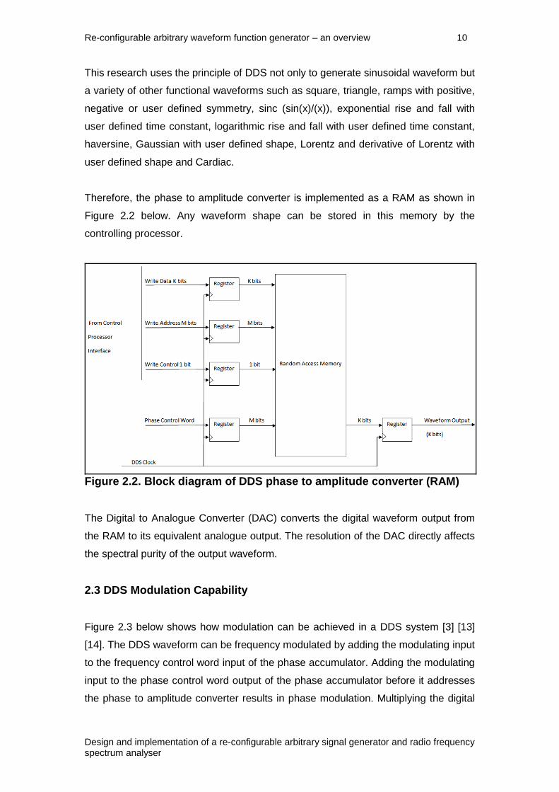
Therefore, the phase to amplitude converter is implemented as a RAM as shown in
Figure 2.2 below. Any waveform shape can be stored in this memory by the
controlling processor.
Figure 2.2. Block diagram of DDS phase to amplitude converter (RAM)
The Digital to Analogue Converter (DAC) converts the digital waveform output from
the RAM to its equivalent analogue output. The resolution of the DAC directly affects
the spectral purity of the output waveform.
2.3 DDS Modulation Capability
Figure 2.3 below shows how modulation can be achieved in a DDS system [3] [13]
[14]. The DDS waveform can be frequency modulated by adding the modulating input
to the frequency control word input of the phase accumulator. Adding the modulating
input to the phase control word output of the phase accumulator before it addresses
the phase to amplitude converter results in phase modulation. Multiplying the digital
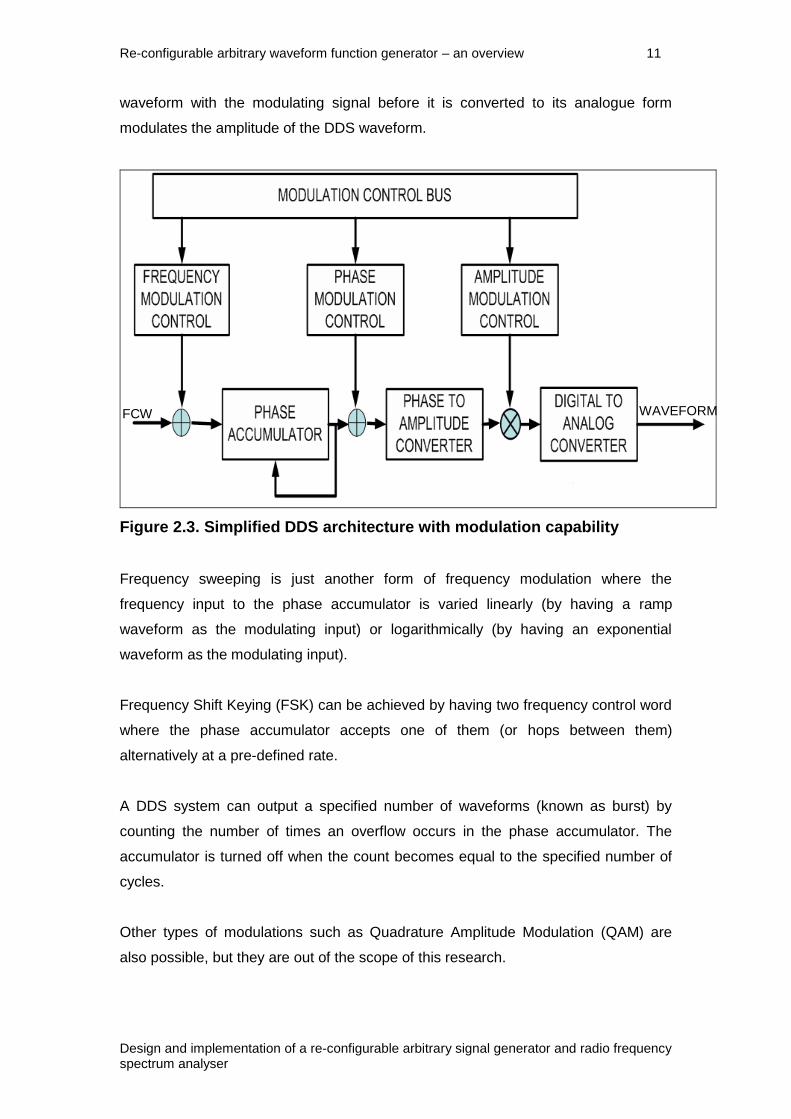
Re-configurable arbitrary waveform function generator – an overview 11
Design and implementation of a re-configurable arbitrary signal generator and radio frequency spectrum analyser
waveform with the modulating signal before it is converted to its analogue form
modulates the amplitude of the DDS waveform.
Figure 2.3. Simplified DDS architecture with modulation capability
Frequency sweeping is just another form of frequency modulation where the
frequency input to the phase accumulator is varied linearly (by having a ramp
waveform as the modulating input) or logarithmically (by having an exponential
waveform as the modulating input).
Frequency Shift Keying (FSK) can be achieved by having two frequency control word
where the phase accumulator accepts one of them (or hops between them)
alternatively at a pre-defined rate.
A DDS system can output a specified number of waveforms (known as burst) by
counting the number of times an overflow occurs in the phase accumulator. The
accumulator is turned off when the count becomes equal to the specified number of
cycles.
Other types of modulations such as Quadrature Amplitude Modulation (QAM) are
also possible, but they are out of the scope of this research.
FCW WAVEFORM

Re-configurable arbitrary waveform function generator – an overview 12
Design and implementation of a re-configurable arbitrary signal generator and radio frequency spectrum analyser
The principle of DDS can be used to generate the internal modulating waveform.
Only phase accumulator and phase to amplitude converter blocks are required. The
output from the phase to amplitude converter is the modulating waveform in its digital
avatar. This is then multiplied by a factor (amplitude depth in case of Amplitude
Modulation (AM), frequency deviation in case of Frequency Modulation (FM), phase
deviation in case of Phase Modulation (PM), frequency span in case of frequency
sweep, etcetera) to have better modulation control. The scaled digital waveform is
then transferred to different parts of the main DDS to perform various modulations.
2.4 DDS Trigger Uncertainty
As mentioned above, a DDS system can output a specified number of waveforms.
This normally happens after a trigger event (internal or external). In case of an
external trigger event, the generation of waveforms begins on the next DDS clock
after the event, which introduces a time uncertainty of up to 1 clock period. This
might not be acceptable in user application.
If the time between the start of the trigger and the start of the subsequent DDS clock
could be measured, then this information could be used to adjust the start phase of
the phase accumulator (by pre-setting the phase control word) and therefore
compensate for the time uncertainty [16]. The FPGA implementation of the particular
method described henceforth to use in a DDS architecture is an original contribution
of this research.
Figure 2.4. Delay line for trigger uncertainty compensation
A tapped delay line shown in Figure 2.4 above could be used to measure the time
between the start of the trigger and the next DDS clock rising or falling edge [17]. The
D6 D7

Re-configurable arbitrary waveform function generator – an overview 13
Design and implementation of a re-configurable arbitrary signal generator and radio frequency spectrum analyser
input to the delay line is the trigger input and the output from each delay tap is
clocked by the DDS clock.
During static condition, all output bits are low. When the trigger arrives, some of the
output bits will change its state from ‘low to high until the delay is long enough for the
rising edge of the trigger signal to move beyond the rising edge of the clock signal
after which point the outputs will remain low. The number of output bits that has
changed state is an indication of the time between the trigger and the clock edge.
As the trigger is delayed, it gets closer to the clock edge and registering it might
suffer from violation of set up times resulting in meta-stability. Therefore, two or more
synchronous register stages should be used instead of one to ensure that the output
is stable and that the probability of an unstable output due to meta-stability is
infinitesimally small.
Figure 2.5. FPGA carry chain implemented as a delay line
In many low cost FPGAs available today, there exist chain structures (carry chain)
that the vendors design for general purpose applications [18] [19]. These chain
structures provide short and predefined routes between identical logic elements.
They are ideal for time to digital converter delay chain implementation [20]. Figure

Re-configurable arbitrary waveform function generator – an overview 14
Design and implementation of a re-configurable arbitrary signal generator and radio frequency spectrum analyser
2.5 above shows how the carry-in and carry-out chain available in most low-cost
FPGAs could be used to implement a delay line for measuring the time between the
start of the trigger and the next DDS clock.
There are certain things to consider here. The logic elements used for the delay
chain and the corresponding register array structure must be placed and routed by
the FPGA compiler in a predictable manner to assure uniformity and short term
stability [20]. The delay of the carry chain is subjected to variation due to temperature
and power supply voltage and therefore needs compensation. The delay of the carry
chain between two logic elements in the same Logic Array Block (LAB) is different
from the delay of the carry chain between two logic elements in two adjacent LABs.
Therefore, if the delay line exceeds beyond a LAB, then the effect of this variation
also needs accounting for. Addressing of the above considerations is discussed in
the next chapter.
2.5 DDS Modulation Using an External Signal
For external modulation, the external modulating waveform is first converted to digital
form by using an Analogue to Digital Converter (ADC). It would be possible to drive
the external modulation ADC with the DDS Clock and have enough bits of resolution
such that the ADC output can directly be used for modulation. However, this is not a
cost effective solution.
The ADC is sampled at a lower rate with fewer bits and therefore some sampling rate
conversion and/or interpolation is required. The Tampere University Paper describes
an interpolation method which could be used in this circumstance [21]. If the ADC
sampling rate is chosen to be some binary division of the DDS clock, then the
difference between two consecutive A/D output samples could be divided by the
same binary factor (a binary factor is chosen so that division just becomes a shifting
operation) and then added to the previous sample at every DDS clock until a new
sample is available.
CIC filters devised by Hogenauer [8] are widely used in communication systems for
efficient sample rate conversions and could also be used to up convert the sampling
rate of the ADC samples to the DDS clock. The key advantage of CIC filters is that
they use only adders and registers, and do not require multipliers to implement in
hardware for handling large rate changes [22].
Re-configurable arbitrary waveform function generator – an overview 15
Design and implementation of a re-configurable arbitrary signal generator and radio frequency spectrum analyser
The performance and hardware complexity of the CIC filter method and the normal
interpolation method to up convert the sampling rate of the external modulating signal
samples are discussed in the simulation section of this chapter and in the
implementation section of the next chapter and is an original contribution of this
research.
2.6 Arbitrary Waveform Generation
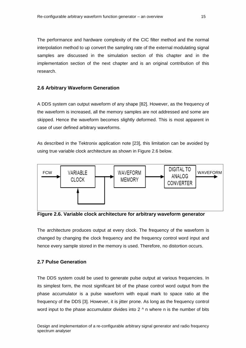
A DDS system can output waveform of any shape [82]. However, as the frequency of
the waveform is increased, all the memory samples are not addressed and some are
skipped. Hence the waveform becomes slightly deformed. This is most apparent in
case of user defined arbitrary waveforms.
As described in the Tektronix application note [23], this limitation can be avoided by
using true variable clock architecture as shown in Figure 2.6 below.
Figure 2.6. Variable clock architecture for arbitrary waveform generator
The architecture produces output at every clock. The frequency of the waveform is
changed by changing the clock frequency and the frequency control word input and
hence every sample stored in the memory is used. Therefore, no distortion occurs.
2.7 Pulse Generation
The DDS system could be used to generate pulse output at various frequencies. In
its simplest form, the most significant bit of the phase control word output from the
phase accumulator is a pulse waveform with equal mark to space ratio at the
frequency of the DDS [3]. However, it is jitter prone. As long as the frequency control
word input to the phase accumulator divides into 2 ^ n where n is the number of bits
FCW WAVEFORM

Re-configurable arbitrary waveform function generator – an overview 16
Design and implementation of a re-configurable arbitrary signal generator and radio frequency spectrum analyser
in the phase accumulator, the output is periodic and smooth, but all other cases will
create jitter [3]. The jitter can vary up to 1 clock period, is fully deterministic and could
be reduced using a delay generator [3]. But a delay generator requires a lot of
hardware and would have been difficult to implement for a single bit pulse output and
even more difficult for multiple bits.
DDS pulse generator architecture has also been proposed by Sullivan et al [24],
which generates multi-bit pulse with independent rise and fall times. But the issue of
jitter has not been dealt with.
It has been proposed in [25] to use a higher frequency clock when the accumulator
overflows to output pulse with less jitter. However, in order to keep the jitter very low,
a very high clock frequency would be required which makes this architecture very
expensive.
It is also possible to generate pulse waveform by counting clock cycles [26]. The
clock used could be a DDS generated clock (DDS sine output generated by the
FPGA, DAC and the re-construction filter and then converted into square waveform
clock using a comparator outside the FPGA) in order to have the ability to slightly
vary the clock frequency to increase pulse period resolution. Clock cycles are
counted to determine period and pulse width. Edge times could be controlled by a
pulse edge shaping circuit in the analogue domain. The drawback of this method is
that the resolution of the pulse width is limited to the clock period.
The focus of this research has been to achieve an entirely digital DDS-based pulse
generator. Generally, the output of the phase accumulator is used to address a RAM
which contains the desired waveform shape. Doing this in a pulse generator would
mean it is not possible to output pulses continuously while parameters are being
changed because it would require re-loading of the RAM. It would also mean that it is
not possible to realise a pulse with very long period and very short width or edge time
due to the limited RAM size [24].
The output of the phase accumulator is a ramp waveform. It is possible to convert
this into a pulse which is essentially a waveform made of four ramp waveforms of
varying slope using mathematical means. Four comparators could be used to convert
the phase accumulator output to different sections of the pulse using a state

Re-configurable arbitrary waveform function generator – an overview 17
Design and implementation of a re-configurable arbitrary signal generator and radio frequency spectrum analyser
machine, a subtractor and a multiplier. The truncated output of the multiplier would
be the desired pulse.
As long as the minimum edge time has enough points to be fully defined, the
waveform would be jitter free. For example, for a 5 ns edge time, in order to have 5
points on the edge, the DDS clock frequency needs to be 800 MHz. Pulse period,
width and delay modulation, is achieved by simply adding the modulating waveform
value to the content of the various comparator control words.
The method described above for digital pulse generation using mathematical means
and its FPGA implementation discussed in the next chapter is an original contribution
of this research work.
2.8 White Noise Generation
Linear Feedback Shift Registers (LFSRs) are generally used to generate pseudo
random noise. Multiple bits can be obtained from LFSRs by using the method
described in [27]. One way to generate white noise using LFSRs has been proposed
in [28] which multiplexes several registers with different initial states to produce
pseudo random numbers. However, the output does not follow a Gaussian
distribution.
Napier [29] also proposed a novel architecture for white noise generation using a
circuit comprising of pseudo random sequence generators, plural delay circuits,
plural finite impulse response filters and a summing network. However, this method is
too complex to be implemented in a small FPGA.
Brian et al [30] first proposed a method to convert the pseudo random sequence into
Gaussian white noise by using a ROM which has stored values of any kind of desired
distribution. Ghazel et al [31] [32] proposed the development of a Gaussian white
noise generator by combining the Box-Muller method and Central-Limit theorem. The
pseudo random sequence is generated by multi bit LFSRs, Box-Muller method is
implemented using ROMs and Central-Limit theorem is implemented by means of an
accumulator. This method produces a high accuracy, fast, low complexity white noise
generator. A similar architecture has also been proposed in [33]. Fung et al [34]
proposed an ASIC implementation of the architecture proposed in [31] and [32].
Re-configurable arbitrary waveform function generator – an overview 18
Design and implementation of a re-configurable arbitrary signal generator and radio frequency spectrum analyser
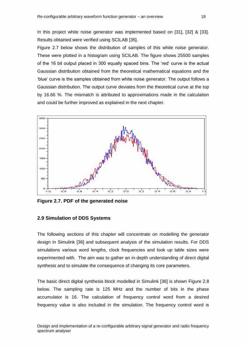
In this project white noise generator was implemented based on [31], [32] & [33].
Results obtained were verified using SCILAB [35].
Figure 2.7 below shows the distribution of samples of this white noise generator.
These were plotted in a histogram using SCILAB. The figure shows 25500 samples
of the 16 bit output placed in 300 equally spaced bins. The ‘red’ curve is the actual
Gaussian distribution obtained from the theoretical mathematical equations and the
‘blue’ curve is the samples obtained from white noise generator. The output follows a
Gaussian distribution. The output curve deviates from the theoretical curve at the top
by 16.66 %. The mismatch is attributed to approximations made in the calculation
and could be further improved as explained in the next chapter.
Figure 2.7. PDF of the generated noise
2.9 Simulation of DDS Systems
The following sections of this chapter will concentrate on modelling the generator
design in Simulink [36] and subsequent analysis of the simulation results. For DDS
simulations various word lengths, clock frequencies and look up table sizes were
experimented with. The aim was to gather an in-depth understanding of direct digital
synthesis and to simulate the consequence of changing its core parameters.
The basic direct digital synthesis block modelled in Simulink [36] is shown Figure 2.8
below. The sampling rate is 125 MHz and the number of bits in the phase
accumulator is 16. The calculation of frequency control word from a desired
frequency value is also included in the simulation. The frequency control word is

Re-configurable arbitrary waveform function generator – an overview 19
Design and implementation of a re-configurable arbitrary signal generator and radio frequency spectrum analyser
converted to an unsigned 16-bit value and all subsequent blocks operate on 16-bit
integer arithmetic.

Re-configurable arbitrary waveform function generator – an overview 20
Design and implementation of a re-configurable arbitrary signal generator and radio frequency spectrum analyser
Figure 2.8. Simulation of 16 bit un-modulated direct digital synthesis

Re-configurable arbitrary waveform function generator – an overview 21
Design and implementation of a re-configurable arbitrary signal generator and radio frequency spectrum analyser
Time Offset
Figure 2.9. Phase accumulator output
Ph
ase C
on
tro
l W
ord
Re-configurable arbitrary waveform function generator – an overview 22
Design and implementation of a re-configurable arbitrary signal generator and radio frequency spectrum analyser
Figure 2.9 above is the phase accumulator output for an input frequency of 1 MHz.
The output is a ramp which increments by frequency control word value at the clock
rate. When the output reaches its maximum value of 65535, it overflows and starts
accumulating again. The rate of overflow is 1 MHz, which is the desired frequency.
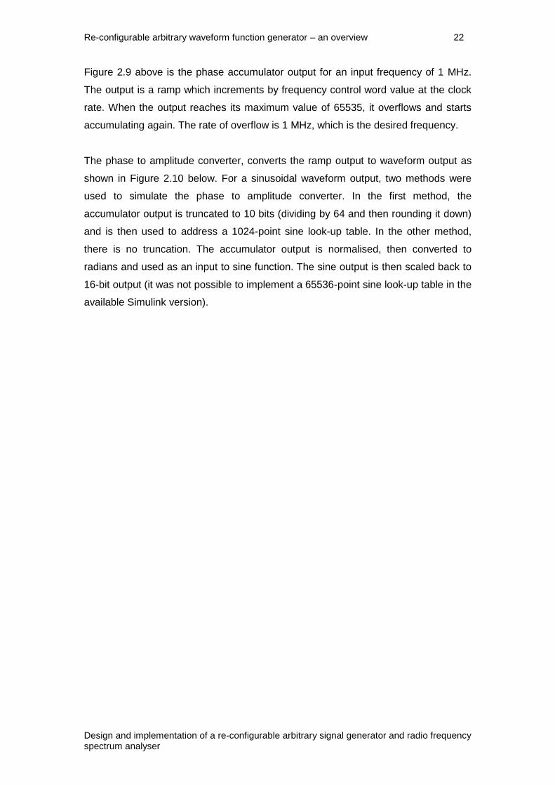
The phase to amplitude converter, converts the ramp output to waveform output as
shown in Figure 2.10 below. For a sinusoidal waveform output, two methods were
used to simulate the phase to amplitude converter. In the first method, the
accumulator output is truncated to 10 bits (dividing by 64 and then rounding it down)
and is then used to address a 1024-point sine look-up table. In the other method,
there is no truncation. The accumulator output is normalised, then converted to
radians and used as an input to sine function. The sine output is then scaled back to
16-bit output (it was not possible to implement a 65536-point sine look-up table in the
available Simulink version).
Re-configurable arbitrary waveform function generator – an overview 23
Design and implementation of a re-configurable arbitrary signal generator and radio frequency spectrum analyser
Time Offset Figure 2.10. Phase to amplitude converter output in the time domain
16
bit S
inu
so
ida
l O
utp
ut
Re-configurable arbitrary waveform function generator – an overview 24
Design and implementation of a re-configurable arbitrary signal generator and radio frequency spectrum analyser
Figure 2.11. Frequency spectrum of the DDS output where accumulator output is truncated to 10 bits

Re-configurable arbitrary waveform function generator – an overview 25
Design and implementation of a re-configurable arbitrary signal generator and radio frequency spectrum analyser
Figure 2.12. Frequency spectrum of the DDS output where accumulator output is not truncated

Re-configurable arbitrary waveform function generator – an overview 26
Design and implementation of a re-configurable arbitrary signal generator and radio frequency spectrum analyser
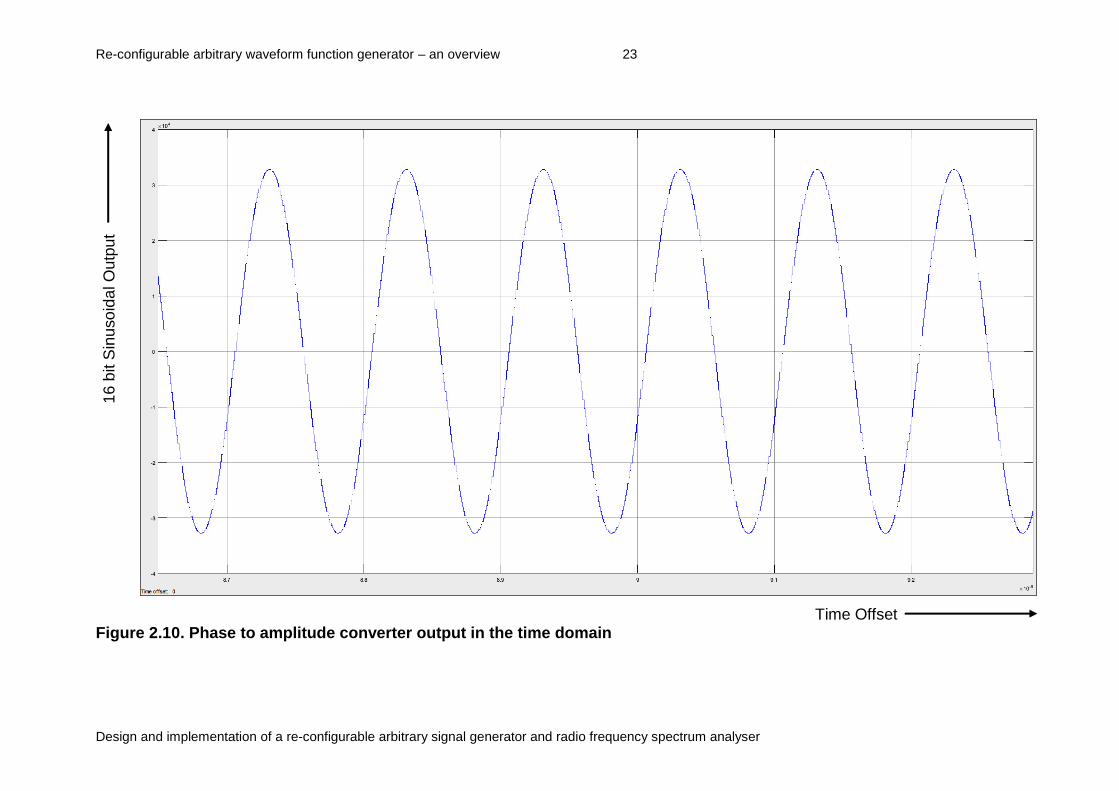
The frequency spectrum of the two phase to amplitude converters addressed with
truncated and un-truncated accumulator outputs are shown in Figure 2.11 and Figure
2.12 above respectively. When the accumulator outputs are truncated they
introduces spurs at the DDS output.
The carrier frequency is 1 MHz. The carrier level is 118 dBm. In Figure 2.11, the
accumulator output is truncated to 10 bits. The harmonic spurs are visible at 7 MHz,
9 MHz, 14 MHz, 17 MHz, 23 MHz and 24 MHz respectively. The harmonic spurs
above 20 MHz are worse than those below 20 MHz and are approximately 78 dB
below carrier level. Non-harmonic spurs are approximately 110 dB below carrier
level. In Figure 2.12, the accumulator output is not truncated. No visible harmonic
spurs are present in the spectrum output. Non-harmonic spurs are approximately
120 dB below carrier level.
In order to achieve fine frequency resolution, a large DDS word length is required.
For a clock frequency of 125 MHz, a 48-bit accumulator provides a frequency
resolution of 0.44 uHz.
The resolution of the DAC directly affects the spectral purity of the waveform output.
Simulation of a 32-bit DDS system with 200 MHz clock frequency and a pre-
calculated frequency control word to output a 25 MHz signal is shown in Figure 2.13
below.

Re-configurable arbitrary waveform function generator – an overview 27
Design and implementation of a re-configurable arbitrary signal generator and radio frequency spectrum analyser
Figure 2.13. Simulation of 32 bit direct digital synthesis

Re-configurable arbitrary waveform function generator – an overview 28
Design and implementation of a re-configurable arbitrary signal generator and radio frequency spectrum analyser
Figure 2.14. Frequency spectrum for 16-bit output

Re-configurable arbitrary waveform function generator – an overview 29
Design and implementation of a re-configurable arbitrary signal generator and radio frequency spectrum analyser
Figure 2.15. Frequency spectrum for 14-bit output

Re-configurable arbitrary waveform function generator – an overview 30
Design and implementation of a re-configurable arbitrary signal generator and radio frequency spectrum analyser
The frequency spectrums of 16-bit system and 14-bit system derived from the same
32-bit DDS accumulators are shown in Figure 2.14 and Figure 2.15 above
respectively. The spurious free dynamic range for a 16-bit output is 96 dB
approximately. The spurious free dynamic range for a 14-bit output is 78 dB
approximately.
2.10 Simulation of modulated DDS
For modulation, a second DDS is simulated to provide the modulating waveform. The
output from the modulating phase to amplitude converter is multiplied by a factor
which controls the modulation depth or deviation. This is then added to the frequency
control word input of the first DDS to perform frequency modulation. The calculation
for a particular frequency deviation is also included in the simulation. The simulation
is shown in Figure 2.16 below.
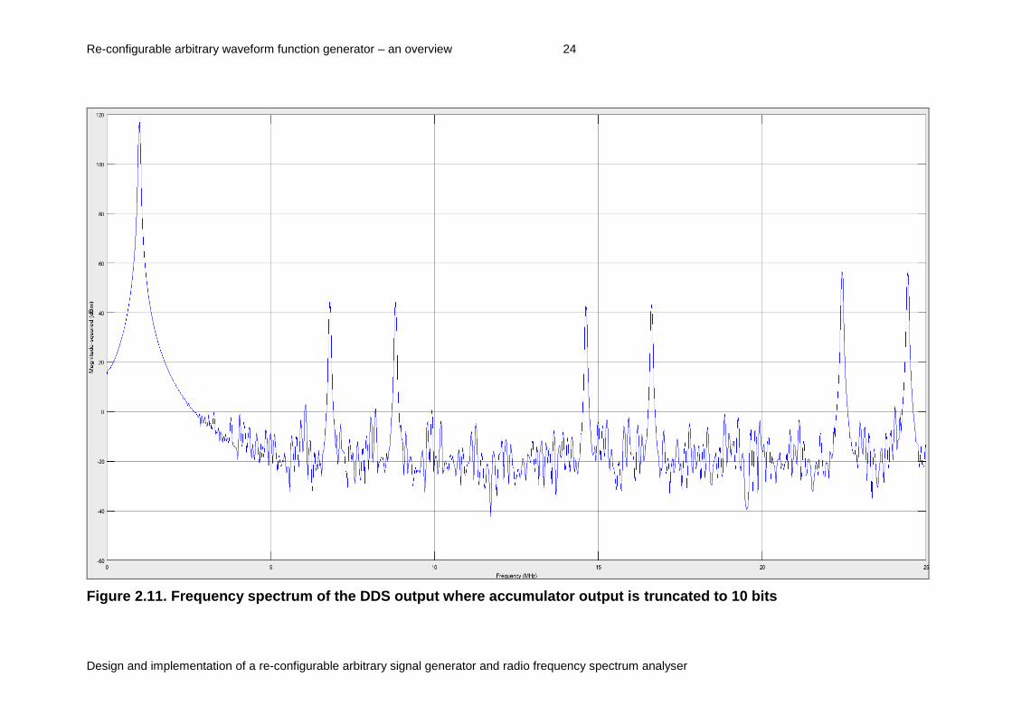
For a carrier frequency of 10 MHz, modulation frequency of 100 kHz and a frequency
deviation of 1 MHz, the frequency spectrum output is as shown in Figure 2.17 below.
Simulink scope settings are as follows:
Start Frequency 0 Hz
Stop Frequency 25 MHz
Window Length 4096
FFT Length 4096
Window Hanning Window
Equivalent Noise Band-width 1.5
Trace Normal Trace
Units dBm

Re-configurable arbitrary waveform function generator – an overview 31
Design and implementation of a re-configurable arbitrary signal generator and radio frequency spectrum analyser
Figure 2.16. Simulation of frequency modulation in a DDS system
Re-configurable arbitrary waveform function generator – an overview 32
Design and implementation of a re-configurable arbitrary signal generator and radio frequency spectrum analyser
Figure 2.17. Frequency spectrum of a frequency modulated DDS output
Re-configurable arbitrary waveform function generator – an overview 33
Design and implementation of a re-configurable arbitrary signal generator and radio frequency spectrum analyser
For phase modulation, the appropriately scaled output from the second DDS is
added to the output of the phase accumulator of the second DDS as shown in Figure
2.18 below. The calculation for a particular phase deviation is included in the
simulation.
For a carrier frequency of 10 MHz, modulation frequency of 100 kHz and a phase
deviation of 180 degrees, the frequency spectrum output is shown in Figure 2.19
below.
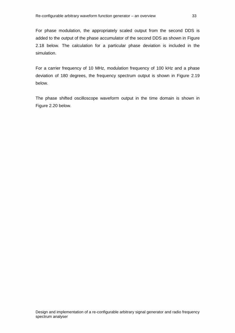
The phase shifted oscilloscope waveform output in the time domain is shown in
Figure 2.20 below.

Re-configurable arbitrary waveform function generator – an overview 34
Design and implementation of a re-configurable arbitrary signal generator and radio frequency spectrum analyser
Figure 2.18. Simulation of phase modulation in a DDS system

Re-configurable arbitrary waveform function generator – an overview 35
Design and implementation of a re-configurable arbitrary signal generator and radio frequency spectrum analyser
Figure 2.19. Frequency spectrum of a phase modulated DDS output
Re-configurable arbitrary waveform function generator – an overview 36
Design and implementation of a re-configurable arbitrary signal generator and radio frequency spectrum analyser
Time Offset Figure 2.20. Phase modulated waveform output in the time domain
16
bit W
ave
form
Ou
tpu
t

Re-configurable arbitrary waveform function generator – an overview 37
Design and implementation of a re-configurable arbitrary signal generator and radio frequency spectrum analyser
For amplitude modulation, the appropriately scaled output from the second DDS is
multiplied with the output of the phase to amplitude converter of the first DDS. This
could be done in one of two ways. Half of the modulation waveform could be added
to half of the amplitude and the result multiplied with the carrier waveform or the
modulating waveform could be directly multiplied with the carrier waveform thereby
controlling its amplitude (suppressed carrier). Both methods were simulated as
shown in Figure 2.21 and Figure 2.24 below respectively.
Figure 2.22 below shows the frequency spectrum of a normal amplitude modulated
sinusoidal waveform, where the carrier frequency is 10 MHz. The frequency of the
modulating sinusoidal waveform is 1 MHz. Amplitude depth is set to 100 %. The two
side-bands and the carrier are present in the output spectrum.
Figure 2.23 below shows the modulating and modulated waveforms for normal
amplitude modulation in the time domain. The modulating frequency is changed from
1 MHz to 100 kHz. The instantaneous voltage of the modulating waveform is added
or subtracted to the user specified amplitude value before being multiplied to the
waveform output. When modulation waveform amplitude is at its minimum, the output
is zero.

Re-configurable arbitrary waveform function generator – an overview 38
Design and implementation of a re-configurable arbitrary signal generator and radio frequency spectrum analyser
Figure 2.21. Simulation of amplitude modulation in a DDS system

Re-configurable arbitrary waveform function generator – an overview 39
Design and implementation of a re-configurable arbitrary signal generator and radio frequency spectrum analyser
Figure 2.22. Frequency spectrum of an amplitude modulated DDS output (carrier is not suppressed)

Re-configurable arbitrary waveform function generator – an overview 40
Design and implementation of a re-configurable arbitrary signal generator and radio frequency spectrum analyser
Time Offset
Figure 2.23. Modulation waveform and amplitude modulated carrier in the time domain
Mo
du
late
d O
utp
ut
M
od
ula
tio
n W
ave
form

Re-configurable arbitrary waveform function generator – an overview 41
Design and implementation of a re-configurable arbitrary signal generator and radio frequency spectrum analyser
Figure 2.25 below shows the frequency spectrum of a suppressed carrier amplitude
modulated sinusoidal waveform, where the carrier frequency is 10 MHz. The
frequency of the modulating sinusoidal waveform is 1 MHz. Amplitude depth is set to
100 %. The frequency spectrum shows the two sidebands but the carrier is
suppressed. The carrier is suppressed by approximately 96 dB. The carrier could be
further suppressed by increasing the number of bits in the phase accumulator.
Figure 2.26 below shows the modulating and modulated waveforms for suppressed
carrier amplitude modulation in the time domain. The modulating frequency is
changed from 1 MHz to 100 kHz. The instantaneous voltage of the modulating
waveform directly controls the amplitude of the waveform output. When modulation
waveform amplitude is zero, the output is zero.

Re-configurable arbitrary waveform function generator – an overview 42
Design and implementation of a re-configurable arbitrary signal generator and radio frequency spectrum analyser
Figure 2.24. Simulation of suppressed carrier amplitude modulation in a DDS system

Re-configurable arbitrary waveform function generator – an overview 43
Design and implementation of a re-configurable arbitrary signal generator and radio frequency spectrum analyser
Figure 2.25. Frequency spectrum of an amplitude modulated DDS output (carrier is suppressed)

Re-configurable arbitrary waveform function generator – an overview 44
Design and implementation of a re-configurable arbitrary signal generator and radio frequency spectrum analyser
Time Offset Figure 2.26. Suppressed carrier amplitude modulation in the time domain
Mo
du
late
d O
utp
ut
M
od
ula
tio
n W
ave
form
Re-configurable arbitrary waveform function generator – an overview 45
Design and implementation of a re-configurable arbitrary signal generator and radio frequency spectrum analyser
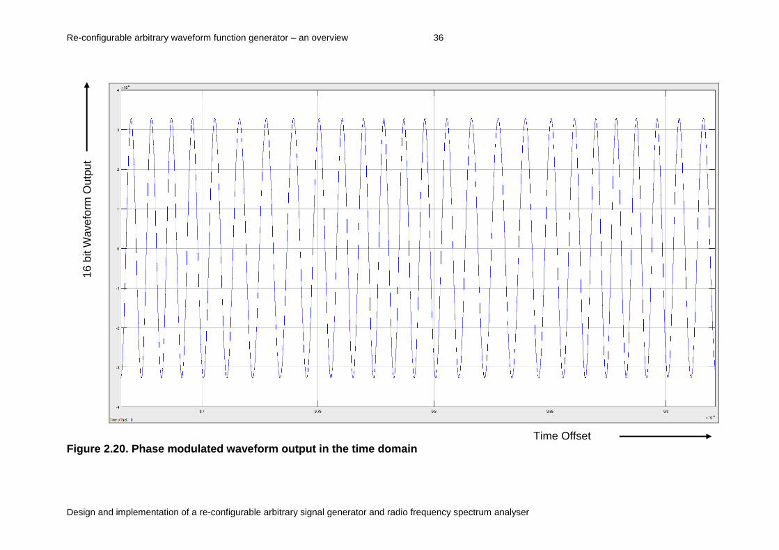
2.11 Simulation of DDS modulation using an external signal
Up-conversion of the sampling rate of the external modulating signal was simulated
using two ways, by interpolation and by using CIC filters.
The sampling rate of the 12-bit ADC is chosen to be 7.8125 MHz such that it is a
binary multiple of the DDS clock frequency which is 125 MHz. This is done to make
the division that is necessary in the interpolation method to be just an exercise of
shifting bits to the left. The ADC output is delayed by one clock cycle. It is then
subtracted from the new sample. This result is then added to the previous sample 16
times unless a new sample arrives and the whole process starts again. The result is
an interpolated version of the original waveform output from the ADC at the DDS
clock frequency. The simulation is shown in Figure 2.27 below.
Figure 2.27. Simulation of sample rate conversion using interpolation
method
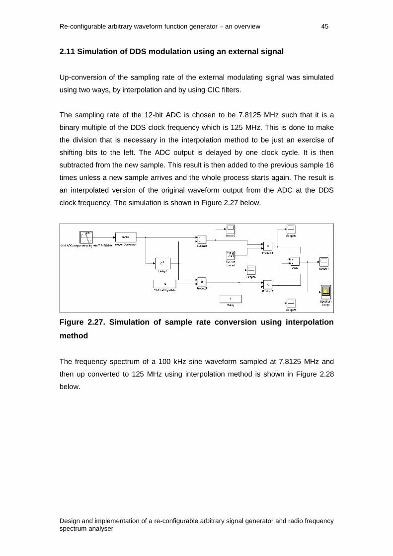
The frequency spectrum of a 100 kHz sine waveform sampled at 7.8125 MHz and
then up converted to 125 MHz using interpolation method is shown in Figure 2.28
below.
Re-configurable arbitrary waveform function generator – an overview 46
Design and implementation of a re-configurable arbitrary signal generator and radio frequency spectrum analyser
Figure 2.28. Frequency spectrum of interpolated waveform output
Re-configurable arbitrary waveform function generator – an overview 47
Design and implementation of a re-configurable arbitrary signal generator and radio frequency spectrum analyser
The interpolation itself does not introduce any spurs. Therefore, as long as the
conversion factor remains binary, interpolation method is a viable method for sample
rate conversion of external modulating signals.
However, a non-binary conversion factor increases the hardware complexity of this
method. A division by a non-binary number is not trivial and adds significantly to the
hardware resource requirements.
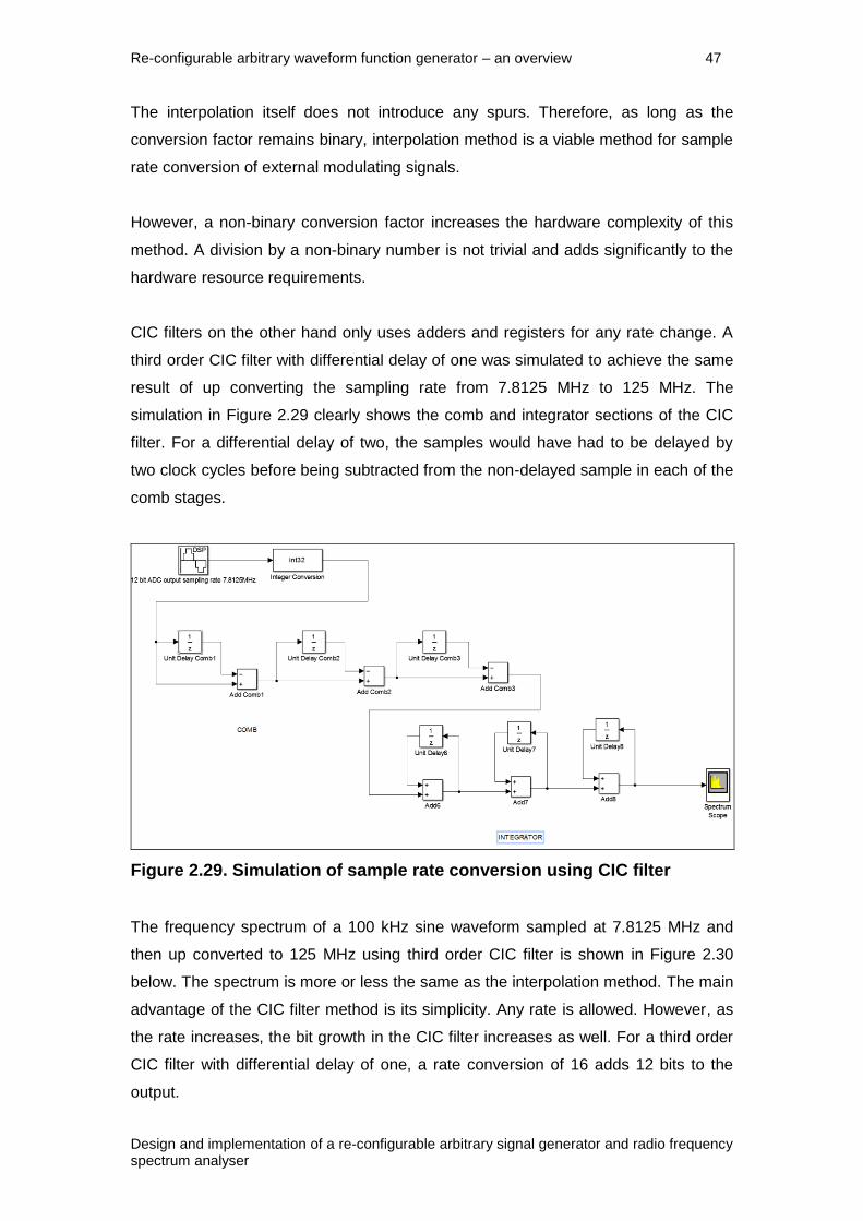
CIC filters on the other hand only uses adders and registers for any rate change. A
third order CIC filter with differential delay of one was simulated to achieve the same
result of up converting the sampling rate from 7.8125 MHz to 125 MHz. The
simulation in Figure 2.29 clearly shows the comb and integrator sections of the CIC
filter. For a differential delay of two, the samples would have had to be delayed by
two clock cycles before being subtracted from the non-delayed sample in each of the
comb stages.
Figure 2.29. Simulation of sample rate conversion using CIC filter
The frequency spectrum of a 100 kHz sine waveform sampled at 7.8125 MHz and
then up converted to 125 MHz using third order CIC filter is shown in Figure 2.30
below. The spectrum is more or less the same as the interpolation method. The main
advantage of the CIC filter method is its simplicity. Any rate is allowed. However, as
the rate increases, the bit growth in the CIC filter increases as well. For a third order
CIC filter with differential delay of one, a rate conversion of 16 adds 12 bits to the
output.

Re-configurable arbitrary waveform function generator – an overview 48
Design and implementation of a re-configurable arbitrary signal generator and radio frequency spectrum analyser
Figure 2.30. Frequency spectrum of CIC filter output

Re-configurable arbitrary waveform function generator – an overview 49
Design and implementation of a re-configurable arbitrary signal generator and radio frequency spectrum analyser
2.12 Conclusion
This chapter demonstrates the feasibility and functional verification of the generator
design. Principles of direct digital synthesis and its modulation capability, arbitrary
waveform, pulse and white noise generation have been discussed and novel ideas
have been presented. The design is simulated in Matlab / Simulink environment and
principles of the design is validated.
The next chapter details the new design analysis of various waveform generation
architectures and interpolation of external modulating signal and FPGA design,
simulation and synthesis of the waveform generator.
Waveform generator – FPGA 50
Design and implementation of a re-configurable arbitrary signal generator and radio frequency spectrum analyser
3 Waveform Generator – FPGA Design Simulation and
Synthesis
3.1 Introduction
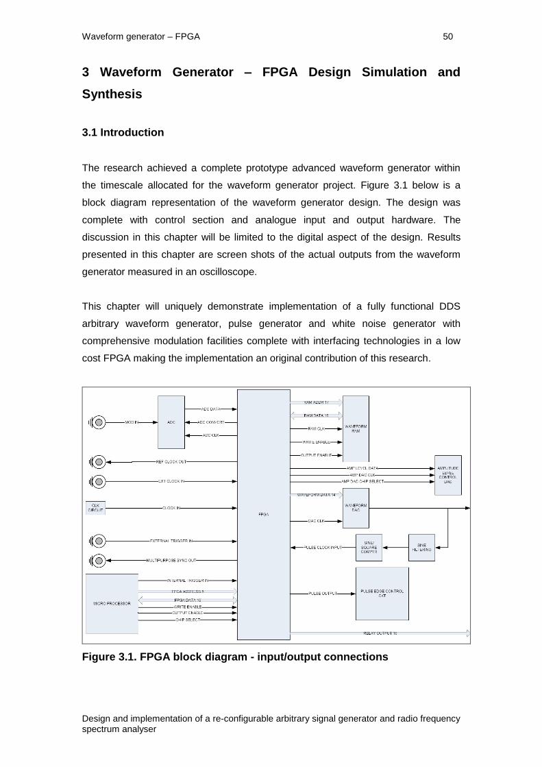
The research achieved a complete prototype advanced waveform generator within
the timescale allocated for the waveform generator project. Figure 3.1 below is a
block diagram representation of the waveform generator design. The design was
complete with control section and analogue input and output hardware. The
discussion in this chapter will be limited to the digital aspect of the design. Results
presented in this chapter are screen shots of the actual outputs from the waveform
generator measured in an oscilloscope.
This chapter will uniquely demonstrate implementation of a fully functional DDS
arbitrary waveform generator, pulse generator and white noise generator with
comprehensive modulation facilities complete with interfacing technologies in a low
cost FPGA making the implementation an original contribution of this research.
Figure 3.1. FPGA block diagram - input/output connections

Waveform generator – FPGA 51
Design and implementation of a re-configurable arbitrary signal generator and radio frequency spectrum analyser
3.2 Evaluation of FPGA Technologies
FPGA was chosen as the suitable platform to implement the digital design. The aim
was to use a low cost FPGA. FPGAs from different manufacturers and of different
families were evaluated. This is summarised here as follows. The information on the
FPGAs provided here were true when the evaluation was carried out. The
specification of the FPGAs may have changed since then. The costs of the FPGAs
were obtained from their respective suppliers in the region. The price quoted is for
each unit if a thousand is purchased in a year.
XC3S250E from Xilinx Spartan III series [37], ECP2-20 from Lattice [38] and EP3C16
from Altera Cyclone III series [39] were identified to closely meet the requirements for
the development of this product. Table 3.1 below presents a rough comparison of
these three FPGAs.
Xilinx Spartan III
XC3S250E [37]
Lattice ECP2-20
[38]
Altera Cyclone III
EP3C16 [39]
Logic Elements 5508 21000 15408
Total RAM 216 Kbits 276 Kbits 504 Kbits
Embedded Multipliers
(18x18)
12 28 56
PLL/DLL/DCM 4 4 4
Cost $13 (obtained from
Xilinx website)
£10.236
(Supplier’s quote)
£6.82 (Supplier’s
quote)
Table 3.1. Comparison of FPGAs
Clearly, the Altera part provided more embedded multipliers and more memory which
were very important for this product. It was also very cheap and hence became more
favourable for this cost sensitive development.
Another FPGA from the Xilinx Spartan III family, 3A-DSP [40] provided more
embedded multipliers but they were more expensive and hence not considered.
Xilinx FPGA XC3S1200E [41] closely resembled Altera FPGA EP3C16 in terms of
the number of logic elements (They provided 19512 logic cells against 15408, 8
Digital Clock Managers (DCMs) against 4 Phase Lock Loops (PLLs) and 28

Waveform generator – FPGA 52
Design and implementation of a re-configurable arbitrary signal generator and radio frequency spectrum analyser
multipliers against 56 provided by EP3C16). But the price of this FPGA was £21.40
(supplier’s quote) and hence not suitable for this product. Spartan 3E family are
based on 90 nm technology.
The Lattice part had more logic elements than the Altera part and also provided
embedded accumulators (not present in Xilinx or Altera part. However, can be easily
designed using the Mega Function Wizard in Quartus or using CoreGen in Xilinx
ISE). However, they provided less memory and multipliers than the Altera part. They
were also more expensive. ECP2-20 is also based on 90 nm technology.
Hence the Altera Cyclone III EP3C16 FPGA was chosen for this design. Cyclone III
is based on 65 nm technology. Choosing an Altera FPGA made the Altera Quartus II
design software [42] the most obvious choice for FPGA design. Altera also provided
ModelSim [43], a comprehensive simulation and debug environment for FPGA
designs. VHDL was predominantly used to model the signal generator system. The
Mega Function Wizard of Quartus II was also used for some specific designs.
Design analysis and implementations of waveform generator sub-systems will be
discussed in this chapter.
3.3 DDS Carrier Generator
Figure 3.2 below represents the Register Transfer Level (RTL) view of the carrier
generator. The carrier generator comprises of a ‘carrier phase accumulator’ the
length of which is 48 bits in order to provide a frequency resolution of 1 µHz in the
system. The clock frequency is 125 MHz.
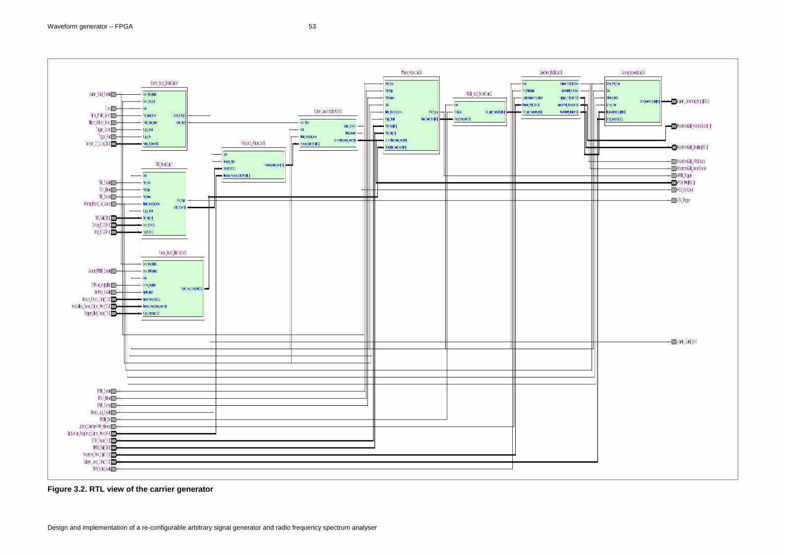
Waveform generator – FPGA 53
Design and implementation of a re-configurable arbitrary signal generator and radio frequency spectrum analyser
Figure 3.2. RTL view of the carrier generator

Waveform generator – FPGA 54
Design and implementation of a re-configurable arbitrary signal generator and radio frequency spectrum analyser
The input 48-bit frequency control word to the frequency control word register of the
phase accumulator is provided by the ‘frequency adder block’. The frequency adder
block adds the output of the ‘FSK block’ and the frequency modulation output of the
‘modulation generator’ block at every clock cycle. When frequency modulation is
disabled, the frequency modulation output from the modulation generator block is
zero and the frequency adder block passes the output of the FSK block at every
clock cycle.
The carrier frequency control word and the hop frequency control word are inputs to
the FSK block which when FSK is enabled hops between the two frequency inputs at
the trigger rate at every clock cycle. The trigger input is the synchronous trigger input.
When FSK is disabled, the FSK block outputs the carrier frequency control word at
every clock cycle.
As mentioned earlier, a DDS system can output a specified number of waveforms.
This normally happens after a trigger event (internal or external). A state machine is
designed to generate a synchronous reset signal to the phase accumulator. When
the trigger event happens, the synchronous reset is de-asserted. The accumulator
starts running. The carry-out from the phase accumulator adder indicates the
completion of a waveform cycle. A counter is incremented on every carry-out. When
the count becomes equal to N-1, where N is the number of specified cycles, the
synchronous reset is asserted and the accumulator stops and then waits for the next
trigger event to start a new burst. Trigger uncertainty compensation is discussed later
in this chapter.
The 16 Most Significant Bits (MSBs) of the phase accumulator output is added with
phase modulation output of the modulation generator, the phase of the carrier
waveform and trigger uncertainty compensation phase factor is subtracted from the
phase accumulator output at every clock cycle in the ‘phase adder’ block. A few
pipeline stages are introduced to process the various additions and subtractions.
The output of the phase adder is the read address input to the ‘waveform RAM
block’. The chosen FPGA for this project provides embedded dual port RAM which is
directly instantiated as the waveform RAM block. The write address and data is
loaded in the RAM by the controlling processor. The output of the RAM is the
waveform output.

Waveform generator – FPGA 55
Design and implementation of a re-configurable arbitrary signal generator and radio frequency spectrum analyser
The ‘output block’ multiplies the waveform output and the amplitude control word at
every clock cycle. When amplitude modulation is enabled, the amplitude control word
could either be the amplitude modulation output of the modulation generator or could
be the sum of half of the modulation generator output and half of the specified
amplitude of the waveform. The former results in suppressed carrier amplitude
modulation and the latter method results in normal double sideband amplitude
modulation respectively. When amplitude modulation is disabled, the amplitude
control word is the specified amplitude of the waveform.
The DAC converts the digital waveform output from the output block to its equivalent
analogue output. Figure 3.3 below shows the FPGA and DAC connection of the
hardware. The DAC fitted on the board is a communication DAC AD9744 from
Analog Devices [44].
Figure 3.3. FPGA DAC connections
3.4 DDS Modulation Generator
The modulation generator provides inputs for modulation operations. Figure 3.4
below is the RTL view of the modulation generator.
External High-Speed Synchronous RAM
FPGA
Control Processor
Digital to Analogue Converter

Waveform generator – FPGA 56
Design and implementation of a re-configurable arbitrary signal generator and radio frequency spectrum analyser
Figure 3.4. RTL view of the modulation generator

Waveform generator – FPGA 57
Design and implementation of a re-configurable arbitrary signal generator and radio frequency spectrum analyser
It generates an internal modulating waveform using the principles of DDS. The
‘modulation source select’ block selects between internally generated waveform,
external modulation input and noise to be used as modulating input.
The output of this block is then multiplied by a factor to control amplitude depth,
frequency deviation or phase deviation. This multiplication is not trivial. For a 48 bit
accumulator, the output from the source select block which is 16 bit has to be
multiplied by a 48 bit control word resulting in a 64 bit output which is then truncated
to 48 bits resulting in modulation frequency control word. A solution to large
multiplication is presented by J W Lewis [45] where the first stage performs partial
multiplications, the outputs of which are shifted and added in pipeline stages. The 48
bit control word is divided in three 16 bit control words and each is multiplied with the
16 bit modulating waveform. The results from each multiplication is shifted and then
added together to produce the final result.
The control word for phase and amplitude modulation is only 16 bits as they are
added to the truncated 16 bit phase accumulator output or multiplied with the 16 bit
carrier waveform output respectively. Therefore, the multiplication could be
performed in one clock cycle.
The output of the deviation-depth multiplier is passed on to various registers. Each
type of modulation has its own synchronous reset signal to control the output from its
corresponding register. When a particular modulation is enabled, its register outputs
the multiplier output. When disabled, output from the register is zero.
3.5 White Noise Generator
Figure 3.5 below is the block diagram of the white noise generator which combines
Box-Muller [46] method and the central limit theorem to produce white noise. White
noise generator implementation is based on [31], [32] & [33].
Linear feedback shift registers are used to produce pseudo random binary variable to
be used to perform the Box-Muller algorithm. A total of 7 LFSRs are used. 6 of them
are used to calculate function F(x) and 1 is used to calculate the function G(x). Table
3.2 below outlines the number of shift registers, characteristic polynomial and initial
seed value of each of the seven LFSRs used in the white noise generator.

Waveform generator – FPGA 58
Design and implementation of a re-configurable arbitrary signal generator and radio frequency spectrum analyser
LFSR Number of Shift Registers Characteristic Polynomial Seed Value
1 31 1+(x)28+(x)31 2147483647
2 19 1+(x)2+(x)6+(x)19 524287
3 13 1+(x)3+(x)4+(x)13 8191
4 7 1+(x)6+(x)7 127
5 5 1+(x)2+(x)5 31
6 7 1+(x)6+(x)7 127
7 17 1+(x)14+(x)17 131071
Table 3.2. LFSR configurations in the white noise generator
LFSRs 1, 2, 3, 4, 5 & 6 are used to produce a 4-bit output to be used to compute the
function F(x) and LFSR 7 is used to produce an 8-bit output to be used to compute
the function G(x).
Multiple bits are produced using the ‘Leap-Forward’ [27] techniques. The leap
forward LFSR method utilizes one LFSR and shifts out several bits. This method is
based on the observation that LFSR is a linear system and the register state can be
written in the vector format:
)()1( iQAiQ (3.1)
)1( iQ and )(iQ are the content of the shift registers at thi )1( and thi)( steps
and A is the transition matrix.
After the LFSR advances n cycles, the equation becomes:
Q(i + n) = An × Q(i) (3.2)
Hence for a 4 bit output, calculation of A4 is required and for an 8 bit output,
calculation of A8 is necessary for each LFSR. After the matrix calculation, Xor
structure for each LFSR is determined accordingly.
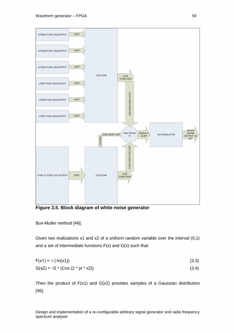
Waveform generator – FPGA 59
Design and implementation of a re-configurable arbitrary signal generator and radio frequency spectrum analyser
LFSR31 FOR LOGOUTPUT
LFSR19 FOR LOGOUTPUT
LFSR7 FOR LOGOUTPUT
LFSR7 FOR LOGOUTPUT
LFSR5 FOR LOGOUTPUT
LFSR13 FOR LOGOUTPUT
LFSR 17 FOR COS OUTPUT COS ROM
LOG ROM
MULTIPLIE
RACCUMULATOR
4 BIT
8 BIT
RESULT
16 BIT
COS
FUNCTION
WHITE
NOISE
OUTPUT 16
BIT
CO
S F
UN
CT
ION
8 B
IT
LOG
FUNCTION
4 BIT
4 BIT
4 BIT
4 BIT
4 BIT
LO
G F
UN
CT
ION
8 B
IT
COS SIGN 1 BIT
CO
SS
IG
Figure 3.5. Block diagram of white noise generator
Box-Muller method [46]:
Given two realizations x1 and x2 of a uniform random variable over the interval (0,1)
and a set of intermediate functions F(x) and G(x) such that:
F(x1) = √ (-ln(x1)) (3.3)
G(x2) = √2 * (Cos (2 * pi * x2)) (3.4)
Then the product of F(x1) and G(x2) provides samples of a Gaussian distribution
[46].

Waveform generator – FPGA 60
Design and implementation of a re-configurable arbitrary signal generator and radio frequency spectrum analyser
The greatest non-linearities of the function F(x) lies in the region close to 0 and 1
[33]. The segment (0, 1) is divided and pre-computed values are stored in ROM1.
LFSR1 is used to provide the address values to this ROM. The first sub segment
near zero is further divided and its pre-computed values are stored in ROM2. This
process is repeated 5 times to get enough resolutions for the region close to zero.
The last sub segment close to one is also divided to account for non linearities in the
region close to one.
The function G(x) is relatively straight-forward. LFSR7 is used to provide the address
values for this ROM. Pre-computed values of the Cos function are stored in the
ROM. Owing to the symmetric properties of Cos function only quarter of the points
are stored thereby reducing the ROM size by 75 %. Multiplication by √2 is dropped
from the equation. The reasons are explained below. The Cos ROM is also used to
produce a sign bit for the multiplier.
The outputs from the two functions are multiplied to obtain the final result. The result
is presented in 2’s complement form when the sign is 1.
Central limit theorem states that given a sequence of realizations of independent and
identically distributed random variables x1, x2, to xn with unit variance and zero
mean, the distribution of: (x1 + x2 + ... + xn) / √n tends to be normally distributed as n
→ ∞ [33]. If n is equal to two, then the central limit theorem will require division by √2,
which is not easy to implement in hardware. Fortunately, since computation of G(x)
involves a multiplication by √2, this multiplication is in effect cancelled by the
subsequent division, so it can be removed from both places in the implementation
[33].

Waveform generator – FPGA 61
Design and implementation of a re-configurable arbitrary signal generator and radio frequency spectrum analyser
Figure 3.6. RTL view of the noise generator

Waveform generator – FPGA 62
Design and implementation of a re-configurable arbitrary signal generator and radio frequency spectrum analyser
Figure 3.6 above shows the RTL view of the white noise generator implemented in
the FPGA. The probability density function of the generated noise is shown in Figure
2.7 in the previous chapter. The ‘mismatch’ between the samples near zero can be
minimized by having more resolutions in the Log ROM and/or Cos ROM. The results
can also be improved by accumulating more samples in the accumulator block (by
increasing ‘n’ in the central limit theorem).
The output from the linear feedback shift registers are random in nature and are
uniformly distributed. The Box-Muller method converts this uniformly distributed noise
to a normal distributed noise with mean zero and standard deviation one. Therefore,
this method can only produce Gaussian white noise. If a different distribution is
required, then this method is not ideal.
It is possible to replace this architecture by one multi-bit LFSR with large number of
shift registers addressing a RAM the memory content of which determines the
distribution of the output signal [47]. The advantage of this method is that any
distribution is possible. The user defined distribution can be stored in this memory by
the controlling processor. For Gaussian distribution, the RAM is filled by the inverse
of the normal cumulative distribution for mean zero and standard deviation one.
3.6 Pulse Generator
For a pulse generator shown in Figure 3.7 below, the waveform is generated by
mathematical means. The output of the phase accumulator is not truncated. The
ramp waveform output of the phase accumulator is converted to a pulse by using
comparators, multipliers and a state machine.
A pulse waveform has four transition points, low level to rising edge, rising edge to
high level, high level to falling edge and falling edge to low level. These transition
points correspond to four different values on the phase accumulator output slope.
Four comparators are used to compare the output of the phase accumulators with
the four transition points. A state machine then uses the output of the comparators to
output a pulse waveform and a multiplying factor.

Waveform generator – FPGA 63
Design and implementation of a re-configurable arbitrary signal generator and radio frequency spectrum analyser
Figure 3.7. RTL view of the pulse generator
Waveform generator – FPGA 64
Design and implementation of a re-configurable arbitrary signal generator and radio frequency spectrum analyser
State machine conditions:
If the phase accumulator output is less than the first transition point, then
output is low and multiplying factor is equal to zero.
If the phase accumulator output is more than the first transition point and less
than the second transition point, then output is the difference between the
phase accumulator output and the second transition point and multiplying
factor is equal to the rise-time control word.
If the phase accumulator output is more than the second transition point and
less than the third transition point, then output is high and multiplying factor is
equal to one.
If the phase accumulator output is more than the third transition point and less
than the fourth transition point, then output is the inverse of the difference
between the phase accumulator output and the third transition point and
multiplying factor is equal to the fall-time control word.
If the phase accumulator output is more than the fourth transition point, then
output is low and multiplying factor is equal to zero.
The resultant pulse output has fixed slope. This is then multiplied with the multiplying
factor to give pulse with user defined rise and fall time.
Pulse period is defined by the frequency control word. All other pulse parameters,
delay, width, rise time and fall time is controlled by defining the four transition points
and the rise time and fall time control words all of which is set by the controlling
processor.
It is also very easy to introduce pulse related modulation in this architecture. Pulse
width modulation is achieved by adding the modulation generator output (pulse width
deviation is set in the modulation multiplier) to the third and fourth transition points.
Pulse delay modulation is achieved by adding the modulation generator output (pulse
delay deviation is set in the modulation multiplier) to all four transition points.
Amplitude, frequency and phase modulation is still performed in the same way as in
a conventional DDS architecture.
The pulse generator is still essentially a DDS system and therefore the issue of jitter
needs to be dealt with. Tektronix application note [48] explains the effects of
sampling on edge detection as shown in Figure 3.8. The same principle applies here.

Waveform generator – FPGA 65
Design and implementation of a re-configurable arbitrary signal generator and radio frequency spectrum analyser
The edge time of the pulse waveform needs to be long enough to have a few
samples of the waveform. If the edge contains five samples of the waveform, the
edge time is accurately reconstructed by the filter. The reconstruction filter will join
the samples in a linear fashion provided that the bandwidth of the filter is greater than
the maximum pulse frequency and less than half the sampling rate of the clock
frequency.
For a minimum edge time of 5 ns, the DDS clock frequency should be 800 MHz to
provide five samples of the waveform on the pulse edge. It is not possible to run the
FPGA core at this frequency. However multiple DDSs could be implemented running
at a lower frequency and then their output could be multiplexed to produce the
samples at the higher frequency before being sent to the DAC. The Low Voltage
Differential Signal (LVDS) multiplexing transmitter could run at 840 MHz in a low cost
FPGA and therefore this is an entirely feasible low-cost FPGA solution.
Figure 3.8. Effect of sampling on edge detection [48]
3.7 Arbitrary Waveform Generator
As mentioned earlier, in a true variable clock architecture, where every stored sample
in the memory is generated at clock rate, there is no jitter. The drawback of this

Waveform generator – FPGA 66
Design and implementation of a re-configurable arbitrary signal generator and radio frequency spectrum analyser
method is that for a complex arbitrary waveform which is defined by lots of points, the
maximum frequency that is achievable is limited. For an arbitrary waveform defined
by 256 points, the clock frequency would need to be 12.8 GHz to achieve a
maximum frequency of 50 MHz. This is prohibitively large. The maximum realistic
clock frequency for a low-cost FPGA design using lots of multipliers and a fair
amount of memory is 250 MHz.
It could be argued that if a DDS arbitrary waveform generator distorts the waveform
at higher frequencies as a result of skipped points, a true arbitrary generator
implemented in a low-cost FPGA cannot output a fairly complex arbitrary waveform
for any more than 1 MHz output frequency. Moreover, in a true arbitrary generator, it
is not easy to introduce modulation. The clock itself would be required to be
generated by DDS means to allow modulation.
Therefore, it was decided to stick to the DDS principles for arbitrary waveform
generation as well. The controlling processor simply loads the user defined arbitrary
waveform in the phase to amplitude converter memory. Modulation is carried out in
the normal fashion.
3.8 External Modulation
The external modulating signal is passed through an anti-alias filter before being
digitised by the ADC. The sampling rate of the ADC is chosen to be much smaller
than the DDS clock frequency to keep the cost of the ADC down. For a maximum
modulation frequency of 100 kHz, ADC sampling rate of 7.8125 MHz provides 78
samples for one cycle of the waveform which is sufficient for many fairly complex
waveforms.
Two ways of up-converting the sampling rate of the external modulating signal to the
DDS clock frequency were simulated and their performance and hardware
complexity were analysed.
The CIC filter method was chosen for this research because of its simplicity. Figure
3.9 below is the RTL view of the CIC filter based up-converter. The 7.8125 MHz clock
for the ADC is derived from the 125 MHz DDS clock using a clock divider. Therefore,
the ADC data is synchronous to the DDS clock frequency. The input data is passed
through a CIC filter to provide samples at every DDS clock frequency.

Waveform generator – FPGA 67
Design and implementation of a re-configurable arbitrary signal generator and radio frequency spectrum analyser
Figure 3.9. RTL view of the CIC filter
Clock Enable Generator used
in Comb Section
Comb Section Integrator Section

Waveform generator – FPGA 68
Design and implementation of a re-configurable arbitrary signal generator and radio frequency spectrum analyser
A third order CIC filter with differential delay of one, up-converting the sampling rate
from 7.8125 MHz to 125 MHz for a pass-band frequency of 100 kHz would provide
alias or image attenuation of more than 100 dB [8].
For a CIC filter of order N, differential delay M, and rate change R, the number of
output bits is equal to
Bout = Bin + N * log 2 (R * M) (3.5)
Where Bout is the number of output bits and Bin is the number of input bits. Therefore,
the bit growth is 12 bits. For a 10-bit ADC this implies that all the additions and
subtractions in the CIC filter should be carried out in 22 bits. The output of the CIC
filter is truncated to 16 bits before being used as external source input in the
‘modulation generator’. The number of bits in the CIC filter could have been reduced
by pruning techniques documented in [8] but this was not necessary. The FPGA had
no problem performing 22-bit arithmetic at 125 MHz.
The CIC filter does not have a wide flat pass-band. But for a 100 kHz pass-band at
7.8125 MHz sampling rate, the droop in amplitude is only 0.01 dB [8]. Therefore,
there was no need for any compensation.
3.9 Trigger Uncertainty Compensation
When external signal is used to trigger the generation of waveform, the time between
the start of the trigger and its registration on the next clock event is measured.
The trigger signal is connected to the carry input of a logic element block in the
FPGA. The carry out from the Logic Element (LE) is connected to the carry in of the
following logic element and this process is continued for a number of logic elements
to form a delay chain. Each of the logic elements is configured to perform addition of
‘0’ and ‘1’ and the carry input. The result is registered. When the trigger is low, the
register output is high. When the trigger is high, the output is low and the carry
propagates through. The number of low register outputs on the next clock cycle is a
measure of the time between trigger arrival and clock.
Waveform generator – FPGA 69
Design and implementation of a re-configurable arbitrary signal generator and radio frequency spectrum analyser
Figure 3.10. RTL view of the trigger uncertainty compensation block
Figure 3.10 above is the RTL view of the delay chain implemented in the FPGA to
measure trigger uncertainty. The carry-in-carry-out propagation delay for the chosen
FPGA was 60 ps approximately. Therefore, trigger uncertainty could theoretically be
reduced from 1 clock period to 60 ps.
There are 16 logic elements in a LAB. The delay chain extends beyond many LABs.
The propagation delay between logic elements within a LAB is different from
propagation delay between LABs which could be as long as 180 ps. This difference
is compensated by having two delay chains [15]. The trigger input to the second

Waveform generator – FPGA 70
Design and implementation of a re-configurable arbitrary signal generator and radio frequency spectrum analyser
delay chain is delayed slightly by passing through some combinational logic. This
delay will make the trigger cross the LABS at different times in the two chains. This
time difference is then used to actually measure and sub-divide LAB propagation
delay in multiples of LE propagation delay.
The carry chain propagation delay of each LE will vary with temperature and process
variations. In order to compensate for this the delay line is made long enough to
allow two clock edges to happen. The clock period is divided by the number of low
register outputs between the two clock edges to give a measure of the delay of each
LE. This is measured continuously and therefore account for temperature variations.
256 logic elements in the delay chain were found to be enough to accommodate two
clock edges for a clock frequency of 200 MHz.
Instead of relying on the FPGA fitter tool to place the logic elements in the FPGA, the
logic elements are placed manually next to each other in the FPGA chip planner as
shown in Figure 3.11 below. This is done to make the behaviour of the delay line
predictable and repeatable in a production environment.
Once the trigger uncertainty is measured, it is multiplied by the frequency control
word to convert it into a phase value. This is then subtracted from the output of the
phase accumulator to provide uncertainty compensation of the trigger.
The process of the calculation and compensation of trigger uncertainty introduces
trigger latency, the time when the trigger arrives to the time when the trigger is
actually used. This latency is several clock periods long. Trigger latency is not known
to be a problem as long as it is fixed.

Waveform generator – FPGA 71
Design and implementation of a re-configurable arbitrary signal generator and radio frequency spectrum analyser
Figure 3.11. Trigger delay line placement in the FPGA
Delay Line 1
Delay Line 2

Waveform generator – FPGA 72
Design and implementation of a re-configurable arbitrary signal generator and radio frequency spectrum analyser
3.10 FPGA Microprocessor Interface
A microcontroller communicates with the FPGA to set carrier frequency control word,
modulation frequency control word, modulation depth or deviation control word,
carrier amplitude control word, etcetera. The controlling processor is memory
mapped to the FPGA. The communication does not have to be very fast. These
control words do not have to be changed on the fly.
Figure 3.12. FPGA microprocessor interface
In this research, the selected processor had built in external memory interface which
was ideal to communicate with the FPGA. Figure 3.12 above shows the connections
between the processor and the FPGA. The FPGA had its own dedicated chip enable
from the processor for exclusive communication. When chip enable and write enable
is low, the processor writes the 16-bit data on the 16-bit bi-directional data bus at the
address specified by the 8-bit address bus. When chip enable and output enable is
low, the processor reads the 16-bit data on the 16-bit bi-directional data bus from the
address specified by the 8-bit address bus.
The 8-bit address bus allows reading and writing of 256 16-bit control words which is
more than sufficient for this application. The processor reads and writes
asynchronously to the FPGA. However, the read and write cycles are slow.
Therefore, it is not difficult to synchronise the control words to the FPGA clock.

Waveform generator – FPGA 73
Design and implementation of a re-configurable arbitrary signal generator and radio frequency spectrum analyser
If the control word that the processor needs to write is more than 16-bit wide which is
the case for a 48-bit frequency control word for example, the processor sends the
control word in chunks. In this example, the processor will write to three locations to
set the frequency control word.
If the individual control words are used immediately, there is a potential of setting
incorrect frequency momentarily while the processor is updating the frequency
control word. This could be avoided by having two sets of registers in the FPGA,
namely buffer registers and active registers. The processor updates the buffer
registers and the active register is only updated when all buffer registers are updated.
This allows for glitch-free frequency changes.
When lots of control words define a waveform, which is the case for a pulse
waveform where period, width, delay, rise and fall times needs to be defined, the
active registers could be updated only when all the buffer registers update defining
the waveform is completed. So the waveform would never glitch when any or all of its
parameters are being changed. This is an advantage and necessary in some critical
applications.
The interface doesn’t necessarily have to be parallel. It could have been a Serial to
Parallel Interface (SPI). It just means that the update of waveform parameters would
have been slow and update of waveform RAM might have been prohibitively slow
compared to a parallel interface.
This concludes the discussion of various waveform generator sub-systems.
Waveform generator – FPGA 74
Design and implementation of a re-configurable arbitrary signal generator and radio frequency spectrum analyser
Figure 3.13. RTL view of the overall waveform generator

Waveform generator – FPGA 75
Design and implementation of a re-configurable arbitrary signal generator and radio frequency spectrum analyser
3.11 FPGA Synthesis
The previous section charts the design considerations and implementation of the
waveform generator design. Figure 3.13 above is the RTL view of the complete
waveform generator. Once the design was verified, it was synthesized using Quartus
II in a Cyclone III FPGA (EP3C16F484C7). The summary of synthesis is presented in
Table 3.3 below.
Flow Status Successful - Mon Jan 05 13:59:08 2014
Quartus II Version 13.1 Build 163 10/23/2013 SJ Web
Edition
Revision Name KTPFunction_Generator_TopLevel
Top-level Entity Name KTPFunction_Generator_TopLevel
Family Cyclone III
Device EP3C16F484C7
Timing Models Final
Met timing requirements Yes
Total logic elements 2,772 / 15,408 ( 18 % )
Total combinational functions 1,489 / 15,408 ( 10 % )
Dedicated logic registers 2,466 / 15,408 ( 16 % )
Total registers 2466
Total pins 102 / 347 ( 29 % )
Total virtual pins 0
Total memory bits 278,528 / 516,096 ( 54 % )
Embedded Multiplier 9-bit elements 15 / 112 ( 13 % )
Total PLLs 2 / 4 ( 50 % )
Table 3.3. Quartus flow summary for the generator project
Following synthesis, the design was fitted in the FPGA. The design was analysed to
check whether it meets the timing requirements or not. Finally, programming files
were generated to allow programming or configuring the device. All of these
procedures were performed by the Quartus II software tool provided by Altera.
The design was also analysed to find out how much power it will consume using
‘Power Play Power Analyzer Tool’ in Quartus II. The results were then passed on to
the analogue design engineer in the company for power supply designs.

Waveform generator – FPGA 76
Design and implementation of a re-configurable arbitrary signal generator and radio frequency spectrum analyser
A schematic was then prepared for the FPGA. Input and output signals were
assigned to various pins in the FPGA. Synthesis was carried out again to check the
validity of the assignments. Figure 3.14 below shows the pin assignment of the
signals.
Figure 3.14. FPGA pin assignment – top level view
Schematic was prepared so that the FPGA can be configured in Joint Test Action
Group (JTAG) programming mode using ‘Altera Universal Serial Bus (USB) Blaster’
during the development stages and in Passive Serial (PS) programming mode via the
micro controller during production. The schematic was prepared using configuration
application note [49] provided by Altera. Finally, FPGA interface to micro controller
and other analogue hardware were finalised.
After preparing the FPGA schematic for the instrument, all the different sections,
namely the micro controller based control section, the analogue output hardware and
the FPGA section were integrated to prepare the complete waveform generator
schematic. The Printed Circuit Board (PCB) layout was then prepared and the

Waveform generator – FPGA 77
Design and implementation of a re-configurable arbitrary signal generator and radio frequency spectrum analyser
prototype was built, followed by the testing and validation of the functional prototype.
The generator prototype board is shown in Figure 3.15 below.
Figure 3.15. Waveform generator prototype board
3.12 Results
ModelSim provided by Altera was used to simulate and debug the VHDL design. The
simulation results of some design are presented here.
Figure 3.16 below shows the output waveform from the phase accumulator. It can be
seen that for some arbitrary input value, the output of the phase accumulator
increases linearly on the rising edge of every DDS clock (8 ns in this case). When the
accumulator crosses its maximum value (the accumulator produces a carry output
signal at this point), it overflows and starts increasing again from start.

Waveform generator – FPGA 78
Design and implementation of a re-configurable arbitrary signal generator and radio frequency spectrum analyser
Figure 3.17 below shows the output from the noise generator. It can be seen that for
every clock input the white noise generator produces a random output.
The simulation results for the pulse generator are shown in Figure 3.18 below. The
frequency control word, four comparator control words and rise and fall edge control
words were set to produce a pulse waveform of period 1 us, delay of 100 ns, width of
400 ns, rise time of 100 ns and fall time of 150 ns. The output shown in the
simulation results verify the settings.
The overall design and all the generator sub system were verified in a similar fashion
using ModelSim simulation and/or Quartus simulation tools.
Waveform generator – FPGA 79
Design and implementation of a re-configurable arbitrary signal generator and radio frequency spectrum analyser
Figure 3.16. Simulation results for the carrier phase accumulator

Waveform generator – FPGA 80
Design and implementation of a re-configurable arbitrary signal generator and radio frequency spectrum analyser
Figure 3.17. Simulation results for white noise generator
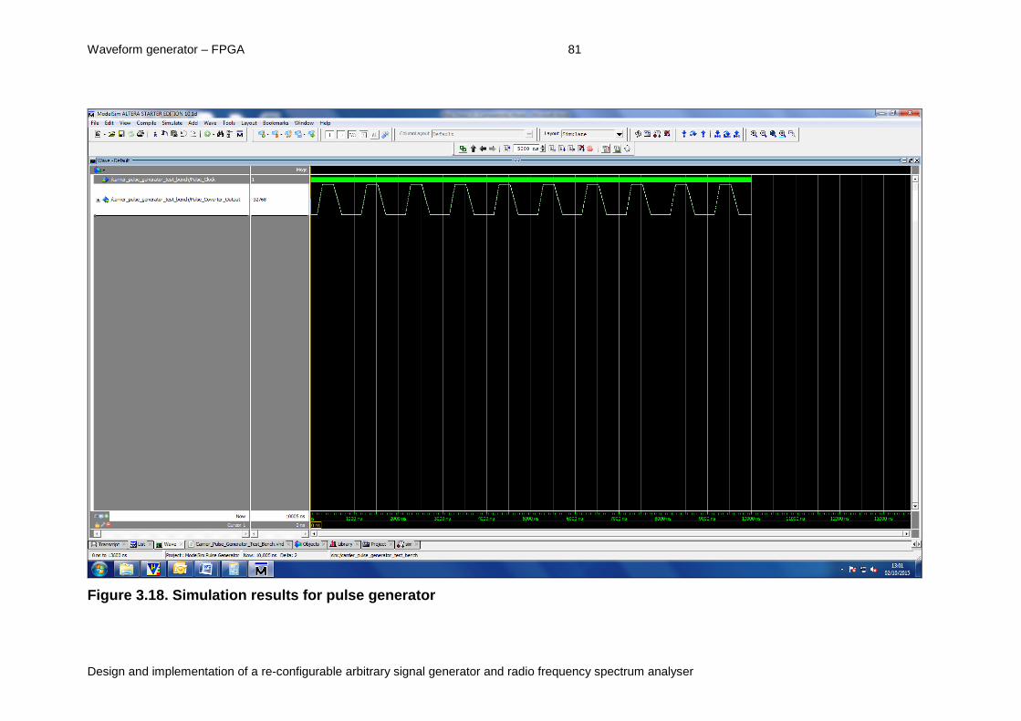
Waveform generator – FPGA 81
Design and implementation of a re-configurable arbitrary signal generator and radio frequency spectrum analyser
Figure 3.18. Simulation results for pulse generator

Waveform generator – FPGA 82
Design and implementation of a re-configurable arbitrary signal generator and radio frequency spectrum analyser
The output waveforms from the prototype board were analysed. Results are
presented in this section.
Figure 3.19. Spectrum of a 25.01 MHz un-modulated DDS sine waveform
The spectrum of a 25.01 MHz sine wave generated by the design with 200 MHz DDS
clock frequency and 32 bits in the phase accumulator and measured using an Anritsu
MS2602A [87] spectrum analyser is shown in Figure 3.19 above. The result is
presented to demonstrate spectral purity of the sine waveform output. It was
observed that the amplitude of the output waveform affected the DDS spur levels.
When the amplitude was at its maximum or near maximum the spur levels were
higher. Reducing the amplitude by 3 dB reduces the spur levels by approximately
10 dB. This could be attributed to the non-linear characteristic of the DAC.
The following figures are measured output from a Tektronix MSO2012 [88]
oscilloscope where the waveforms are generated by the prototype board. Figure 3.20
below shows a 1 MHz DDS sine waveform in the time domain. This demonstrates
that the instrument is capable of generating sinusoidal waveforms. The frequency of
the sine wave can be set from 1 uHz to 50 MHz.
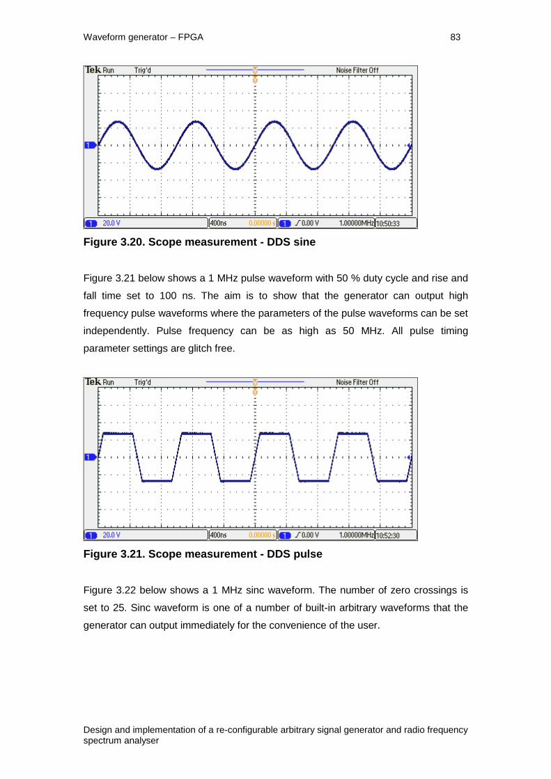
Waveform generator – FPGA 83
Design and implementation of a re-configurable arbitrary signal generator and radio frequency spectrum analyser
Figure 3.20. Scope measurement - DDS sine
Figure 3.21 below shows a 1 MHz pulse waveform with 50 % duty cycle and rise and
fall time set to 100 ns. The aim is to show that the generator can output high
frequency pulse waveforms where the parameters of the pulse waveforms can be set
independently. Pulse frequency can be as high as 50 MHz. All pulse timing
parameter settings are glitch free.
Figure 3.21. Scope measurement - DDS pulse
Figure 3.22 below shows a 1 MHz sinc waveform. The number of zero crossings is
set to 25. Sinc waveform is one of a number of built-in arbitrary waveforms that the
generator can output immediately for the convenience of the user.
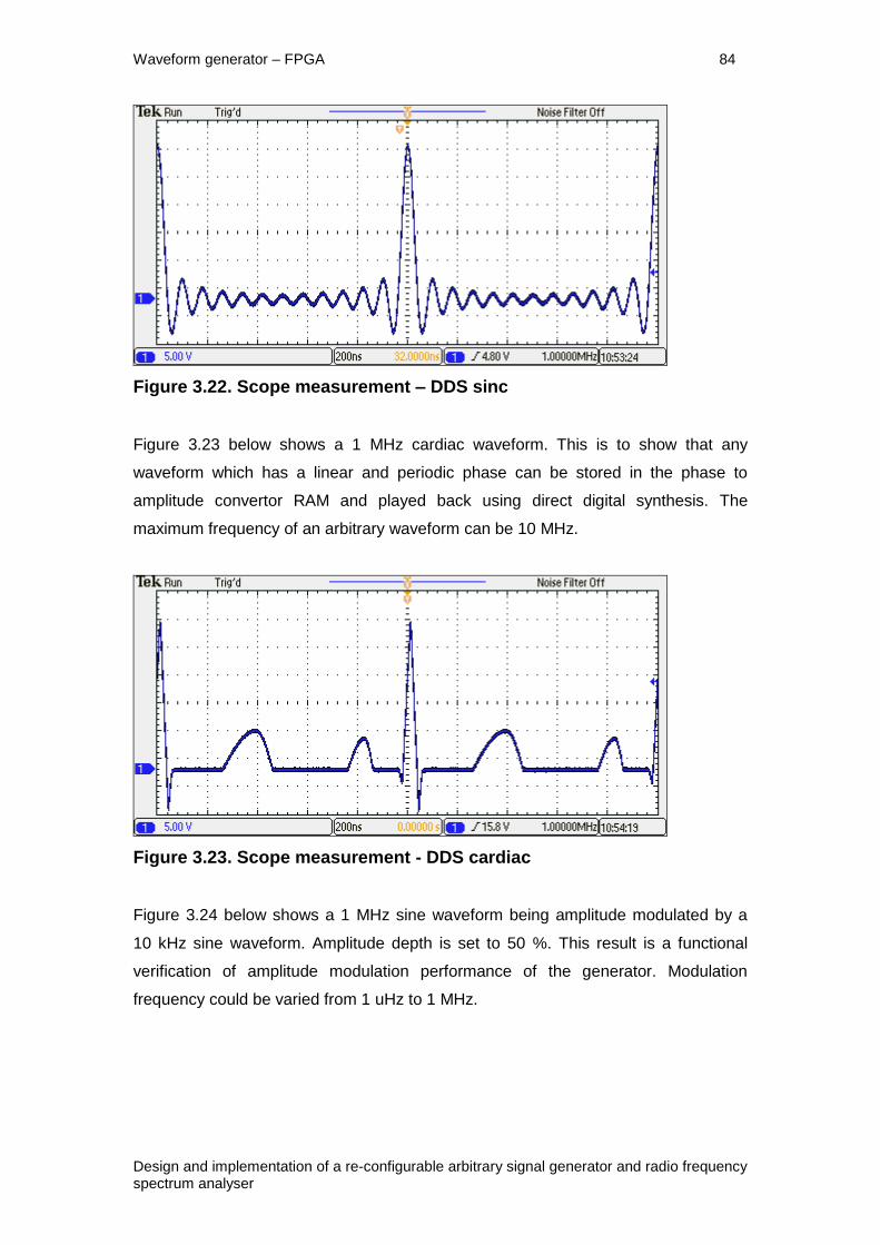
Waveform generator – FPGA 84
Design and implementation of a re-configurable arbitrary signal generator and radio frequency spectrum analyser
Figure 3.22. Scope measurement – DDS sinc
Figure 3.23 below shows a 1 MHz cardiac waveform. This is to show that any
waveform which has a linear and periodic phase can be stored in the phase to
amplitude convertor RAM and played back using direct digital synthesis. The
maximum frequency of an arbitrary waveform can be 10 MHz.
Figure 3.23. Scope measurement - DDS cardiac
Figure 3.24 below shows a 1 MHz sine waveform being amplitude modulated by a
10 kHz sine waveform. Amplitude depth is set to 50 %. This result is a functional
verification of amplitude modulation performance of the generator. Modulation
frequency could be varied from 1 uHz to 1 MHz.
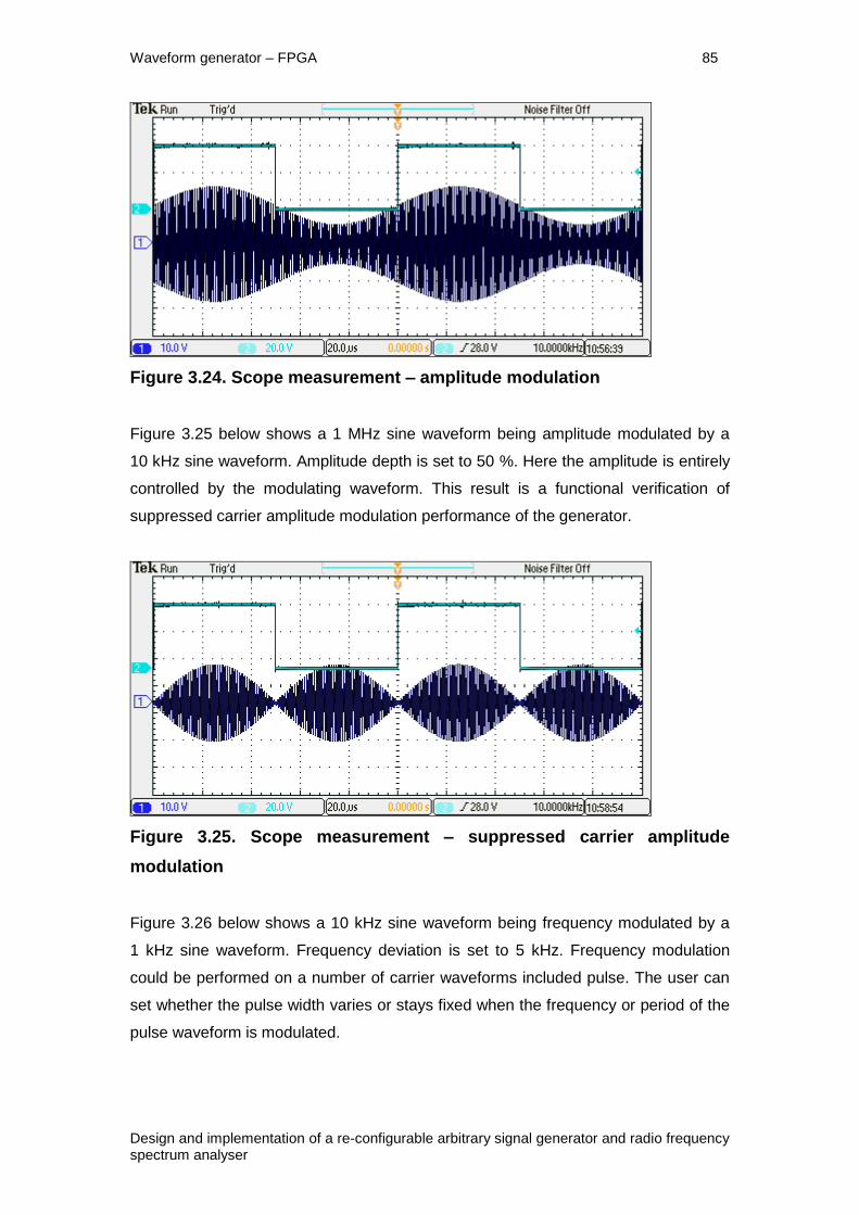
Waveform generator – FPGA 85
Design and implementation of a re-configurable arbitrary signal generator and radio frequency spectrum analyser
Figure 3.24. Scope measurement – amplitude modulation
Figure 3.25 below shows a 1 MHz sine waveform being amplitude modulated by a
10 kHz sine waveform. Amplitude depth is set to 50 %. Here the amplitude is entirely
controlled by the modulating waveform. This result is a functional verification of
suppressed carrier amplitude modulation performance of the generator.
Figure 3.25. Scope measurement – suppressed carrier amplitude
modulation
Figure 3.26 below shows a 10 kHz sine waveform being frequency modulated by a
1 kHz sine waveform. Frequency deviation is set to 5 kHz. Frequency modulation
could be performed on a number of carrier waveforms included pulse. The user can
set whether the pulse width varies or stays fixed when the frequency or period of the
pulse waveform is modulated.
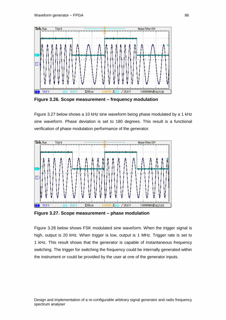
Waveform generator – FPGA 86
Design and implementation of a re-configurable arbitrary signal generator and radio frequency spectrum analyser
Figure 3.26. Scope measurement – frequency modulation
Figure 3.27 below shows a 10 kHz sine waveform being phase modulated by a 1 kHz
sine waveform. Phase deviation is set to 180 degrees. This result is a functional
verification of phase modulation performance of the generator.
Figure 3.27. Scope measurement – phase modulation
Figure 3.28 below shows FSK modulated sine waveform. When the trigger signal is
high, output is 20 kHz. When trigger is low, output is 1 MHz. Trigger rate is set to
1 kHz. This result shows that the generator is capable of instantaneous frequency
switching. The trigger for switching the frequency could be internally generated within
the instrument or could be provided by the user at one of the generator inputs.

Waveform generator – FPGA 87
Design and implementation of a re-configurable arbitrary signal generator and radio frequency spectrum analyser
Figure 3.28. Scope measurement – frequency shift keying
Figure 3.29 below shows a 1 MHz pulse being pulse width modulated by a 1 kHz
sine waveform. Pulse width deviation is set to 100 ns. This demonstrates the pulse
width modulation capabilities of the instrument. Pulse delay modulation is also
possible.
Figure 3.29. Scope measurement – pulse width modulation
Figure 3.30 below shows a triggered 1 MHz pulse waveform. Pulse count is set to
three. On every trigger event three pulses of period 1 us are generated. The output
then remains low until the next trigger event which starts the waveform generation
again. The trigger rate in this instance is set to 100 kHz. This result shows that the
instrument is capable of controlling the start and stops of the generation of waveform
precisely and can do so on a trigger event. The trigger uncertainty is also
compensated for in the generator.

Waveform generator – FPGA 88
Design and implementation of a re-configurable arbitrary signal generator and radio frequency spectrum analyser
Figure 3.30. Scope measurement – triggered pulse
Figure 3.31 below shows white noise output. The crest factor is approximately 3.1.
This validates the noise generator specification of the instrument.
Figure 3.31. Scope measurement – white noise
3.13 Conclusion
The aim of this research was to develop a versatile waveform generator with
specification that matches or exceeds all competition. The research successfully
provides a high-end generator with comprehensive modulation capabilities in the
company’s product range.
This chapter concludes the low-cost signal generator FPGA design.
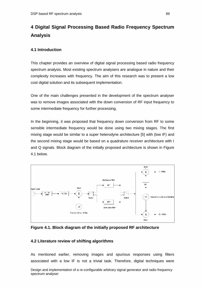
DSP based RF spectrum analysis 89
Design and implementation of a re-configurable arbitrary signal generator and radio frequency spectrum analyser
4 Digital Signal Processing Based Radio Frequency Spectrum
Analysis
4.1 Introduction
This chapter provides an overview of digital signal processing based radio frequency
spectrum analysis. Most existing spectrum analysers are analogue in nature and their
complexity increases with frequency. The aim of this research was to present a low
cost digital solution and its subsequent implementation.
One of the main challenges presented in the development of the spectrum analyser
was to remove images associated with the down conversion of RF input frequency to
some intermediate frequency for further processing.
In the beginning, it was proposed that frequency down conversion from RF to some
sensible intermediate frequency would be done using two mixing stages. The first
mixing stage would be similar to a super heterodyne architecture [5] with (low IF) and
the second mixing stage would be based on a quadrature receiver architecture with I
and Q signals. Block diagram of the initially proposed architecture is shown in Figure
4.1 below.
Figure 4.1. Block diagram of the initially proposed RF architecture
4.2 Literature review of shifting algorithms
As mentioned earlier, removing images and spurious responses using filters
associated with a low IF is not a trivial task. Therefore, digital techniques were

DSP based RF spectrum analysis 90
Design and implementation of a re-configurable arbitrary signal generator and radio frequency spectrum analyser
considered. It was proposed that by shifting LO frequencies the images can be
distinguished from real signals and hence can be removed. A literature search was
carried out to find relevant published articles based on this shifting algorithm. The
findings of this review are briefly summarised here.
The old edition of the Agilent application note on spectrum analysis [50] was found to
be the first document to explain how shifting the LO frequency can distinguish
between a wanted and an image response. If there is a response generated by a LO
frequency, the actual signal could either be at LO – IF or LO + IF. If the LO frequency
is now shifted higher in frequency by twice IF and the response is still there, then the
actual signal is at LO + IF, otherwise, it is at LO – IF. Similarly, if the LO frequency is
shifted lower in frequency by twice IF and the response is still there, then the actual
signal is at LO – IF, otherwise, it is at LO + IF.
The patent by Winter [51] is based on the principle that if the LO frequency is shifted
by an amount (or in other words the IF is shifted by an amount), the actual response is
also shifted by the same amount, whereas the image response will shift by a different
amount and hence can be identified and removed. However, the drawback is that two
IF channels are required.
Koshuge [52] overcomes the two IF channels problem by shifting the LO frequency by
twice IF. The same IF channel can then be used. For a signal at particular sweep
span F1 to F2, the local oscillator is shifted from F1 + FI to F2 + FI (where FI is the
intermediate frequency). The spectrum is generated for this condition. The local
oscillator is then shifted from F1 – FI to F2 – FI and a second spectrum is generated.
For these two spectrums, the IF is the same, but the images fall at different places.
The two spectrums are then compared and for each frequency point, the minimum of
the two data values is selected.
For any shifting algorithm, if the shift is and there are two real signals that are
situated at 2 apart from each other, then the shifting algorithm will not be able to
remove all the images. This is because the generated images fall at the same
frequency point and hence cannot be distinguished. This problem was claimed to be
overcome by Miyauchi [53].

DSP based RF spectrum analysis 91
Design and implementation of a re-configurable arbitrary signal generator and radio frequency spectrum analyser
Miyauchi used more than one IF and for each IF two spectrums were generated. All
the spectrums are then compared and for each frequency point in the spectrum, the
lowest data value is selected [53].
This method reduces the possibility of failure of image detection and removal but does
not completely eliminate it. If the two IFs used are IF1 and IF2 respectively, this
method will not be able to get rid of image responses in the presence of four or more
signals where the first and fourth signals are 4 x IF1 apart, the second and the third
signals are 4 x IF2 apart and the first and the second signals and the third and fourth
signals are 2 x (IF1 – IF2) apart. In complex digital modulation schemes, where there
are lots of frequency components in a spectrum, a shifting algorithm will not provide
the reliability of an image free spectrum response. Moreover, the sweep time
increases by a factor of 2 for each IF which is not ideal.
4.3 Quadrature image reject receiver architecture
Apart from the drawbacks outlined above, in any shifting algorithm, multiple sweeps
have to be carried out which makes it unsuitable for transient signals. Therefore, the
initial proposed architecture was revised. It was suggested that instead of using two
mixing stages, the input range could be divided. A similar architecture to what was
proposed earlier could then be used for the lower range, but using a high IF instead of
a low IF followed by quadrature down conversion. Image spurious associated with a
high IF then could easily be removed using a fixed low-pass filter. For the higher
range, quadrature down conversion could be directly used. Block diagram of the
revised architecture is shown in Figure 4.2 below.
Figure 4.2. Block diagram of the revised RF architecture

DSP based RF spectrum analysis 92
Design and implementation of a re-configurable arbitrary signal generator and radio frequency spectrum analyser
In a quadrature architecture (also known as image rejection mixer architecture), the
images are removed by adding the down converted I and Q (In-phase and
Quadrature-phase) signals one of which is phase shifted by 90 degrees [54]. RF
frequencies are directly converted to base-band (zero IF). However, this introduces
DC offset problems [55]. Therefore, low IF is preferred. However, gain and phase
imbalances in the I and Q channels means the image rejection achieved by a
quadrature receiver is limited to 40 dB [56]. This is improved by applying
compensation for gain and phase imbalances. The novel scheme proposed in this
chapter to remove image frequencies is an original contribution of this research.
4.4 IQ imbalance compensation literature review
A literature search was carried out to find relevant published articles based on IQ
imbalance compensation using digital techniques. Lauder also reviewed some
published articles on image rejection mixers and algorithms for adjusting IQ imbalance
[73].
The algorithms could roughly be divided in two broad categories. In one category, the
gain and phase correction parameters are calculated by using a test signals and then
applied to the real signal, the gain and phase parameters being calibrated periodically
to account for their drifts [67]. This can be described as the calibration method. In the
other category, the parameters are adjusted ‘on the fly’ by correlating the two
channels and converging it to zero [68]. This method is also described as ‘blind
compensation’ method [69]. In the calibration method, an external signal source is
required.
As Lauder mentioned in his review, most of the compensation algorithm concentrate
on a single frequency (or on a very narrow frequency band) [73]. The requirement for
a spectrum analyser is somewhat different. For a spectrum analyser, it will probably
be necessary to divide the frequency range into a large number of sub-bands
(possibly hundreds), not necessarily of equal width. Each sub-band would need its
own parameters for gain mismatch and especially phase mismatch. These parameters
probably need to be stored and some default values may need to set during
manufacture. These parameters can then be periodically updated to account for any
variations in the gain and phase imbalances.
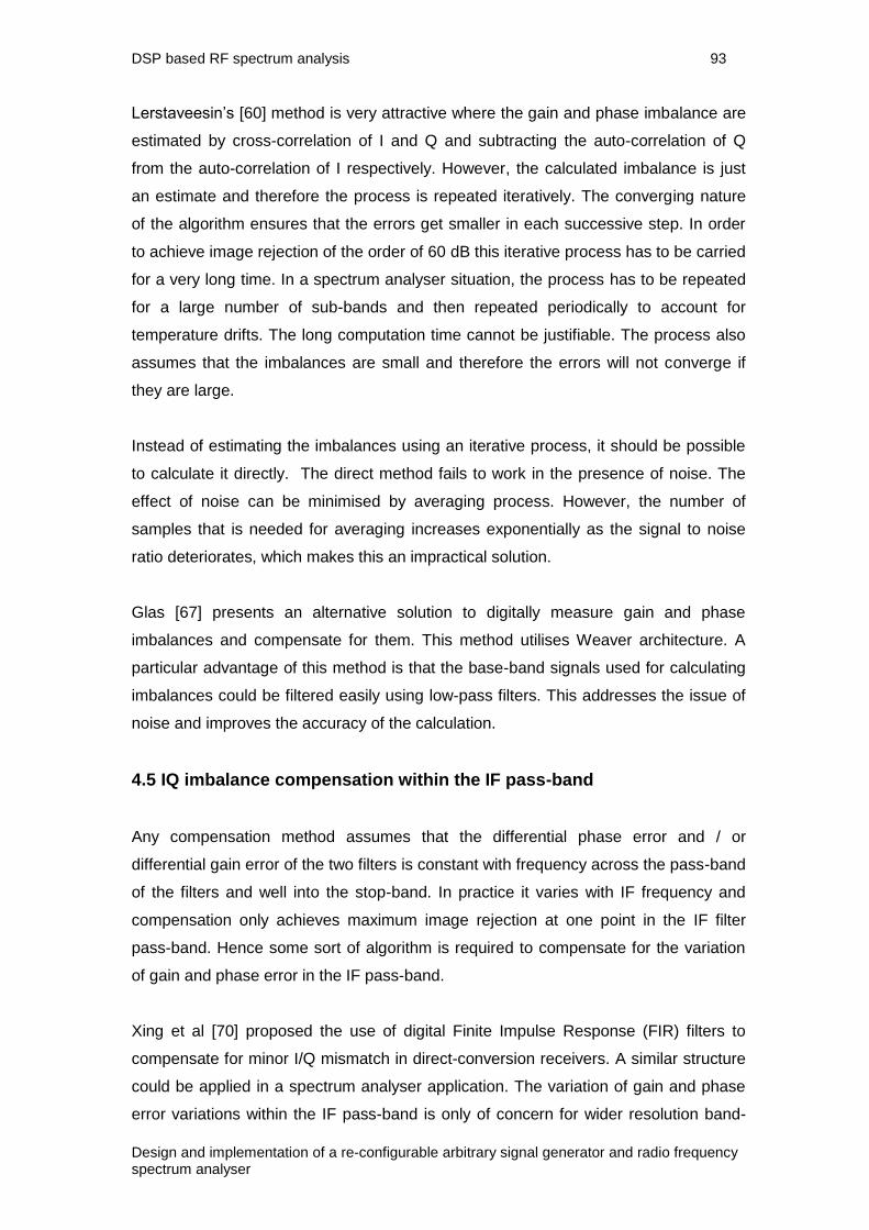
DSP based RF spectrum analysis 93
Design and implementation of a re-configurable arbitrary signal generator and radio frequency spectrum analyser
Lerstaveesin’s [60] method is very attractive where the gain and phase imbalance are
estimated by cross-correlation of I and Q and subtracting the auto-correlation of Q
from the auto-correlation of I respectively. However, the calculated imbalance is just
an estimate and therefore the process is repeated iteratively. The converging nature
of the algorithm ensures that the errors get smaller in each successive step. In order
to achieve image rejection of the order of 60 dB this iterative process has to be carried
for a very long time. In a spectrum analyser situation, the process has to be repeated
for a large number of sub-bands and then repeated periodically to account for
temperature drifts. The long computation time cannot be justifiable. The process also
assumes that the imbalances are small and therefore the errors will not converge if
they are large.
Instead of estimating the imbalances using an iterative process, it should be possible
to calculate it directly. The direct method fails to work in the presence of noise. The
effect of noise can be minimised by averaging process. However, the number of
samples that is needed for averaging increases exponentially as the signal to noise
ratio deteriorates, which makes this an impractical solution.
Glas [67] presents an alternative solution to digitally measure gain and phase
imbalances and compensate for them. This method utilises Weaver architecture. A
particular advantage of this method is that the base-band signals used for calculating
imbalances could be filtered easily using low-pass filters. This addresses the issue of
noise and improves the accuracy of the calculation.
4.5 IQ imbalance compensation within the IF pass-band
Any compensation method assumes that the differential phase error and / or
differential gain error of the two filters is constant with frequency across the pass-band
of the filters and well into the stop-band. In practice it varies with IF frequency and
compensation only achieves maximum image rejection at one point in the IF filter
pass-band. Hence some sort of algorithm is required to compensate for the variation
of gain and phase error in the IF pass-band.
Xing et al [70] proposed the use of digital Finite Impulse Response (FIR) filters to
compensate for minor I/Q mismatch in direct-conversion receivers. A similar structure
could be applied in a spectrum analyser application. The variation of gain and phase
error variations within the IF pass-band is only of concern for wider resolution band-
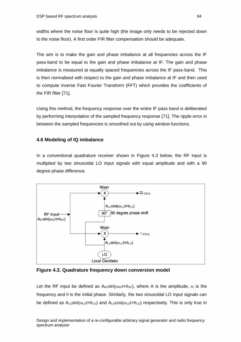
DSP based RF spectrum analysis 94
Design and implementation of a re-configurable arbitrary signal generator and radio frequency spectrum analyser
widths where the noise floor is quite high (the image only needs to be rejected down
to the noise floor). A first order FIR filter compensation should be adequate.
The aim is to make the gain and phase imbalance at all frequencies across the IF
pass-band to be equal to the gain and phase imbalance at IF. The gain and phase
imbalance is measured at equally spaced frequencies across the IF pass-band. This
is then normalised with respect to the gain and phase imbalance at IF and then used
to compute inverse Fast Fourier Transform (FFT) which provides the coefficients of
the FIR filter [71].
Using this method, the frequency response over the entire IF pass band is deliberated
by performing interpolation of the sampled frequency response [71]. The ripple error in
between the sampled frequencies is smoothed out by using window functions.
4.6 Modeling of IQ imbalance
In a conventional quadrature receiver shown in Figure 4.3 below, the RF input is
multiplied by two sinusoidal LO input signals with equal amplitude and with a 90
degree phase difference.
Figure 4.3. Quadrature frequency down conversion model
Let the RF input be defined as ARFsin(RFt+RF), where A is the amplitude, is the
frequency and is the initial phase. Similarly, the two sinusoidal LO input signals can
be defined as ALOsin(LOt+LO) and ALOcos(LOt+LO) respectively. This is only true in

DSP based RF spectrum analysis 95
Design and implementation of a re-configurable arbitrary signal generator and radio frequency spectrum analyser
ideal situation. In reality there always exist an imbalance in the amplitudes and phase
of the two LO input signals.
The output of the mixers will be ARFsin(RFt+RF) x ALOsin(LOt+LO) and
ARFsin(RFt+RF) x ALOcos(LOt+LO). Let these outputs be defined as IIDEAL and QIDEAL
respectively. Therefore,
IIDEAL = ARFsin(RFt+RF) x ALOsin(LOt+LO) (4.1)
QIDEAL = ARFsin(RFt+RF) x ALOcos(LOt+LO) (4.2)
Let be the amplitude imbalance and be the phase imbalance in the LO input
signals. Therefore the LO signals will be ALOsin(LOt+LO) and
ALO(1+)cos(LOt+LO+) respectively.
The output of the mixers will now be
IIDEAL = ARFsin(RFt+RF) x ALOsin(LOt+LO) (4.3)
QREAL = ARFsin(RFt+RF) x ALO(1+)cos(LOt+LO+) (4.4)
In this model, imbalances are placed in the Q channel as shown in Figure 4.4 below.
So any compensation applied to this model will try to match the gain and phase of Q
channel to that of the I channel.
Figure 4.4. Quadrature frequency down conversion model with all
gain/phase imbalances placed in the Q channel

DSP based RF spectrum analysis 96
Design and implementation of a re-configurable arbitrary signal generator and radio frequency spectrum analyser
From trigonometric identities it is known that
cos(x+y) = cos(x)cos(y) - sin(x)sin(y) (4.5)
Hence, QREAL can be expressed as
QREAL = ARFsin(RFt+RF) x ALO(1+)cos(LOt+LO)cos()-sin(LOt+LO)sin() (4.6)
QREAL = ARFsin(RFt+RF) x (1+) ALOcos(LOt+LO)cos() -
ALOsin(LOt+LO)sin() (4.7)
QREAL = (1+)ARFsin(RFt+RF)x ALOcos(LOt+LO)cos() –
ARFsin(RFt+RF) x ALOsin(LOt+LO)sin() (4.8)
ARFsin(RFt+RF) x ALOcos(LOt+LO) and ARFsin(RFt+RF) x ALOsin(LOt+LO) can be
replaced by QIDEAL and IIDEAL respectively.
QREAL = (1+)QIDEALcos() - IIDEALsin() (4.9)
QIDEAL = QREAL / ( cos() (1+) ) + IIDEAL sin() / cos() (4.10)
Therefore as shown in Figure 4.5 below, gain and phase imbalance could be
compensated by multiplying Q channel with 1/(cos()(1-)) and I channel with
sin()/cos() respectively.
Figure 4.5. Compensation model for gain and phase imbalances

DSP based RF spectrum analysis 97
Design and implementation of a re-configurable arbitrary signal generator and radio frequency spectrum analyser
4.7 Modeling of imbalance computation by correlation method
QREAL = (1+)QIDEALcos() - IIDEALsin() (4.11)
Auto-correlation is performed on both sides of the equation (* means correlation)
QREAL * QREAL = (1+)QIDEALcos() - IIDEALsin() *
(1+)QIDEALcos() - IIDEALsin() (4.12)
QREAL * QREAL = (1+)2(QIDEAL * QIDEAL)cos2() + (IIDEAL * IIDEAL)sin2() -
2(IIDEAL * QIDEAL) sin()cos() (4.13)
I and Q are equal orthogonal signals. Therefore, cross-correlation of IIDEAL and QIDEAL
is equal to zero and auto-correlation of IIDEAL is equal to the auto-correlation of QIDEAL
and is equal to the total power in each of the channel [60].
QIDEAL * QIDEAL is replaced by IIDEAL * IIDEAL and IIDEAL * QIDEAL is replaced by 0.
QREAL * QREAL = (1+)2(IIDEAL * IIDEAL)(cos2() + sin2()) (4.14)
From trigonometric identities, it is known that
cos2() + sin2() = 1 (4.15)
Therefore,
QREAL * QREAL = (1+)2(IIDEAL * IIDEAL) (4.16)
1+ = [QREAL * QREAL) / (IIDEAL * IIDEAL)]1/2 (4.17)
Cross-correlation of IIDEAL and QREAL produces the following equation
IIDEAL * QREAL = IIDEAL * [(1+)QIDEALcos() - IIDEALsin()] (4.18)
IIDEAL * QREAL = (1+)cos()(IIDEAL * QIDEAL) - (1+)sin()(IIDEAL * IIDEAL) (4.19)
Cross-correlation of IIDEAL and QIDEAL is equal to zero. Therefore,
IIDEAL * QREAL = -(1+)sin()(IIDEAL * IIDEAL) (4.20)
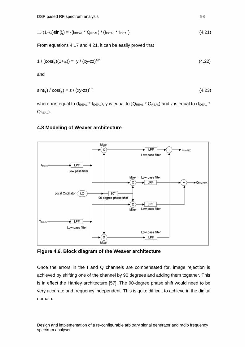
DSP based RF spectrum analysis 98
Design and implementation of a re-configurable arbitrary signal generator and radio frequency spectrum analyser
(1+)sin() = -(IIDEAL * QREAL) / (IIDEAL * IIDEAL) (4.21)
From equations 4.17 and 4.21, it can be easily proved that
1 / (cos()(1+)) = y / (xy-zz)1/2 (4.22)
and
sin() / cos() = z / (xy-zz)1/2 (4.23)
where x is equal to (IIDEAL * IIDEAL), y is equal to QREAL * QREAL) and z is equal to (IIDEAL *
QREAL).
4.8 Modeling of Weaver architecture
Figure 4.6. Block diagram of the Weaver architecture
Once the errors in the I and Q channels are compensated for, image rejection is
achieved by shifting one of the channel by 90 degrees and adding them together. This
is in effect the Hartley architecture [57]. The 90-degree phase shift would need to be
very accurate and frequency independent. This is quite difficult to achieve in the digital
domain.
DSP based RF spectrum analysis 99
Design and implementation of a re-configurable arbitrary signal generator and radio frequency spectrum analyser
Another possible solution is to use a second mixing stage to achieve the 90-degree
phase shift. The intermediate frequency is further down-converted to a lower IF (or
down to base-band). This is described as Weaver architecture [61], shown in Figure
4.6 above. There are several advantages of using Weaver architecture over Hartley in
a FPGA implementation. The down conversion is achieved by using multipliers which
are readily available in FPGAs. The digital filters would also make use of the
embedded multipliers and additions in the filters could be performed using logic
resources.
Assuming that the I and Q signals going into the Weaver architecture are ideal signals
IIDEAL and QIDEAL are defined in equations 4.1 and 4.2 respectively. Equations 4.1 and
4.2 could be re-written as follows.
IIDEAL = (ARFxALO)xcos(RFt+RF-LOt-LO) - cos(RFt+RF+LOt+LO)/2 (4.24)
QIDEAL = (ARFxALO)xsin(RFt+RF+LOt+LO) + sin(RFt+RF-LOt-LO)/2 (4.25)
The anti-alias filter before the ADC will remove the sum frequency component.
Therefore,
IIDEAL = (ARFxALO)xcos(RFt+RF-LOt-LO)/2 (4.26)
QIDEAL = (ARFxALO)xsin(RFt+RF-LOt-LO)/2 (4.27)
IIDEAL = (ARFxALO)xcos((RF-LO)t +(RF-LO))/2 (4.28)
QIDEAL = (ARFxALO)xsin((RF-LO)t +(RF-LO))/2 (4.29)
When the local oscillator is tuned to (RF-LO), a response is generated. A response is
also generated when the local oscillator is tuned to (LO-RF). Therefore, for a signal
present at RF, the tuning of the local oscillator generates two responses. One of
these two responses is an image and should be removed. It is assumed that the
response generated at (RF-LO) is the wanted response and the one generated at
(LO-RF) is the image response.
Let us define (RF-LO) as IF, (RF-LO) as IF, and (ARFxALO)/2 as AIF respectively.
Then, for wanted response,
DSP based RF spectrum analysis 100
Design and implementation of a re-configurable arbitrary signal generator and radio frequency spectrum analyser
IWANTED = AIF x cos(IFt+IF) (4.30)
QWANTED = AIF x sin(IFt+IF) (4.31)
And for image response,
IIMAGE = AIF x cos(-IFt-IF) (4.32)
QIMAGE = AIF x sin(-IFt-IF) (4.33)
From trigonometric identities, it is known that
cos(-a) = cos(a) (4.34)
and
sin(-a) = -sin(a). (4.35)
Therefore,
IIMAGE = AIF x cos(IFt+IF) (4.36)
QIMAGE = AIF x -sin(IFt+IF) (4.37)
The outputs from the four mixers in the Weaver architecture for wanted response are
as follows.
II = AIF x cos(IFt+IF) x sin(LO2t) (4.38)
IQ = AIF x cos(IFt+IF) x cos(LO2t) (4.39)
QI = AIF x sin(IFt+IF) x sin(LO2t) (4.40)
QQ = AIF x sin(IFt+IF) x cos(LO2t) (4.41)
From trigonometric identities, it is known that
cos(a)sin(b) = (sin(a+b) – sin(a-b)) / 2 (4.42) cos(a)cos(b) = (cos(a+b) + cos(a-b)) / 2 (4.43) sin(a)sin(b) = (cos(a-b) – cos(a+b)) / 2 (4.44) sin(a)sin(b) = (sin(a+b) + sin(a-b)) / 2 (4.45)

DSP based RF spectrum analysis 101
Design and implementation of a re-configurable arbitrary signal generator and radio frequency spectrum analyser
Therefore,
II = AIF x sin(IFt+IF+LO2t) - sin(IFt+IF-LO2t) / 2 (4.46)
IQ = AIF x cos(IFt+IF+LO2t) + cos(IFt+IF-LO2t) / 2 (4.47)
QI = AIF x cos(IFt+IF-LO2t) - cos(IFt+IF+LO2t) / 2 (4.48)
QQ = AIF x sin(IFt+IF+LO2t) + sin(IFt+IF-LO2t) / 2 (4.49)
The low-pass filters after the mixers remove the sum frequency component.
Therefore,
II = AIF x -sin(IFt+IF-LO2t) / 2 (4.50)
IQ = AIF x cos(IFt+IF-LO2t) / 2 (4.51)
QI = AIF x cos(IFt+IF-LO2t) / 2 (4.52)
QQ = AIF x sin(IFt+IF-LO2t) / 2 (4.53)
Let us define (LO2-IF) as IF2. Therefore, the four outputs can be written as
II = AIF x sin(IF2t-IF) / 2 (4.54)
IQ = AIF x cos(IF2t-IF) / 2 (4.55)
QI = AIF x cos(IF2t-IF) / 2 (4.56)
QQ = AIF x -sin(IF2t-IF) / 2 (4.57)
It should be noted here that if IF is equal to LO2+IF2, then also it produces the
correct second IF. Therefore, the two low-pass filters are required before the mixers to
provide rejection of this second image.
II is subtracted from QQ to produce IWANTED and IQ and QI are added to produce
QWANTED
IWANTED = AIF x sin(IF2t-IF) (4.58)
QWANTED = AIF x cos(IF2t-IF) (4.59)
DSP based RF spectrum analysis 102
Design and implementation of a re-configurable arbitrary signal generator and radio frequency spectrum analyser
4.9 Modeling of image rejection in Weaver architecture
The outputs from the four mixers in the Weaver architecture for image response are
as follows.
II = AIF x cos(IFt+IF) x sin(LO2t) (4.60)
IQ = AIF x cos(IFt+IF) x cos(LO2t) (4.61)
QI = AIF x -sin(IFt+IF) x sin(LO2t) (4.62)
QQ = AIF x -sin(IFt+IF) x cos(LO2t) (4.63)
Applying equations 4.42, 4.43, 4.44 and 4.45, equations 4.60, 4.61, 4.62 and 4.63 can
be re-written as follows.
II = AIF x sin(IFt+IF+LO2t) - sin(IFt+IF-LO2t) / 2 (4.64)
IQ = AIF x cos(IFt+IF+LO2t) + cos(IFt+IF-LO2t) / 2 (4.65)
QI = AIF x cos(IFt+IF+LO2t) - cos(IFt+IF-LO2t) / 2 (4.66)
QQ = AIF x -sin(IFt+IF+LO2t) - sin(IFt+IF-LO2t) / 2 (4.67)
The low-pass filters after the mixers remove the sum frequency component.
Therefore,
II = AIF x -sin(IFt+IF-LO2t) / 2 (4.68)
IQ = AIF x cos(IFt+IF-LO2t) / 2 (4.69)
QI = AIF x -cos(IFt+IF-LO2t) / 2 (4.70)
QQ = AIF x -sin(IFt+IF-LO2t) / 2 (4.71)
II is subtracted from QQ to produce IWANTED and IQ and QI are added to produce
QWANTED
IWANTED = II – QQ (4.72) QWANTED = IQ + QI (4.73)
IWANTED = 0 (4.74)
QWANTED = 0 (4.75)

DSP based RF spectrum analysis 103
Design and implementation of a re-configurable arbitrary signal generator and radio frequency spectrum analyser
Therefore, the Weaver architecture rejects the image response.
4.10 Modeling of Weaver base-band architecture
The wanted I and Q signal outputs from the Weaver architecture could be converted
down to base-band using a Digital Down Conversion (DDC) architecture for further
processing [17]. Resolution band width filters can then be implemented using low-
pass filters. However, it is also possible to convert the I and Q signals directly down to
base-band in the Weaver architecture itself. Doing this has several advantages. The
two low-pass filters before the mixers are no longer required as there is no second
image. The four low-pass filters after the mixers also functions as RBW filters and
therefore there is no need for any additional filtering thereby reducing design
complexity. Weaver base-band architecture is shown in Figure 4.7 below.
Figure 4.7. Block diagram of the Weaver base-band architecture
4.11 Modeling of imbalance computation using Weaver base-band
architecture
The correlation method of direct computation of gain and phase imbalances does not
work well in the presence of noise. The effect of noise can be minimised by averaging
process. However, the number of samples that is needed would have to increase
exponentially as the signal to noise ratio deteriorates, which makes this an impractical
solution.
DSP based RF spectrum analysis 104
Design and implementation of a re-configurable arbitrary signal generator and radio frequency spectrum analyser
An alternative solution is to calculate imbalances using Weaver base-band
architecture. For imbalance calculation, uncompensated I and Q signals are inputs to
the Weaver base-band architecture.
IIDEAL = AIFcos(IFt+IF) (4.76)
QREAL = AIF(1+)sin(IFt+IF+) (4.77)
The four outputs from the mixers are
II = AIFcos(IFt+IF) x sin(IFt) (4.78)
IQ = AIFcos(IFt+IF) x cos(IFt) (4.79)
QI = AIF(1+)sin(IFt+IF+) x sin(IFt) (4.80)
QQ = AIF(1+)sin(IFt+IF+) x cos(IFt) (4.81)
Applying equations 4.42, 4.43, 4.44 and 4.45, equations 4.78, 4.79, 4.80 and 4.81 can
be re-written as follows.
II = AIFsin(IFt+IF+IFt) + sin(IFt-IFt-IF)/2 (4.82)
IQ = AIFcos(IFt+IF+IFt) + cos(IFt+IF-IFt)/2 (4.83)
QI = AIF(1+)cos(IFt+IF+-IFt) - cos(IFt+IF++IFt)/2 (4.84)
QQ = AIF(1+) sin(IFt+IF+IFt) + sin(IFt+IF+IFt)/2 (4.85)
The low-pass filters will reject the sum frequency components. Therefore,
II = AIFsin(IF)/2 (4.86)
IQ = AIFcos(IF)/2 (4.87)
QI = AIF(1+)cos(IF+)/2 (4.88)
QQ = AIF(1+)sin(IF+)/2 (4.89)
The four outputs still retain the amplitude and phase imbalance information. The aim
is to calculate 1/(cos()(1+)) and sin()/cos(). Solving equations 4.86, 4.87, 4.88
and 4.89, it can be proved that
1/(cos()(1+)) = - ((II x II) + (IQ x IQ)) / ((IQ x QI) – (II x QQ)) (4.90)

DSP based RF spectrum analysis 105
Design and implementation of a re-configurable arbitrary signal generator and radio frequency spectrum analyser
and
sin()/cos() = ((II x QI) + (IQ x QQ)) / ((IQ x QI) – (II x QQ)) (4.91)
The main advantage of using this algorithm is that the four mixer outputs are base-
band signals and hence the low-pass filters can be implemented as very narrow filters.
Therefore, noise can be filtered out and the compensation parameters can be
calculated with great accuracy. Figure 4.8 below is a block diagram representation of
imbalance computation and correction in Weaver base-band architecture. This
proposed method of image suppression is unique and original.
Figure 4.8. Imbalance computation method using Weaver base-band
architecture
4.12 Simulation of imbalance computation by correlation method
The auto correlation of P is equal to (P1*P1+P2*P2+……PN*PN) / N and the cross-
correlation of P and Q is equal to (P1*Q1+P2*Q2+…PN*QN) / N where N is the number
of samples. For the equations derived in the previous section to be true, the cross
correlation of the ideal I and Q channels should be equal to zero (orthogonal property
of I and Q) and the auto correlation of the ideal I channel should be equal to the auto
correlation of the ideal Q channel (and should be equal to the total power in each
channel). These conditions are only satisfied when the numbers of samples used to
calculate the correlations represent exact number of complete waveform cycles of I
and Q.
The error detection block modelled in Simulink is shown in Figure 4.9 below. The
sampling rate is 10 ns and the frequency of the calibration signal used for error

DSP based RF spectrum analysis 106
Design and implementation of a re-configurable arbitrary signal generator and radio frequency spectrum analyser
calculation is equal to 18.75 MHz. Therefore 16 samples will represent exactly 3
cycles of the I and Q waveforms. The ‘Sine wave’ block provides the two calibration
signals (amplitude = 32767, frequency = 18.75 MHz), which are separated by the
‘Select Columns’ block. The phase difference between the two signals is not exactly
90 degrees. A phase error of -0.1 (5.7296 degrees) radians has been introduced. The
two ‘Gain’ blocks multiply the signals by 1 and 0.76143 respectively to introduce a
gain error of 0.23857 (23.857 %). The ‘Dbl to Int16’ and ‘Shift right-2’ blocks are there
to simulate the effects of ADC truncation to 14 bits. The ‘Product’, ‘Cumulative sum’
and ‘Shift right-4’ blocks calculates the correlations (shifting right can be used instead
of division as dividing by 16 is equal to shifting right by 4 bits).
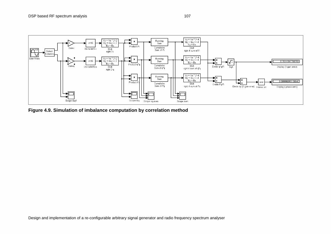
DSP based RF spectrum analysis 107
Design and implementation of a re-configurable arbitrary signal generator and radio frequency spectrum analyser
Figure 4.9. Simulation of imbalance computation by correlation method

DSP based RF spectrum analysis 108
Design and implementation of a re-configurable arbitrary signal generator and radio frequency spectrum analyser
The outputs of the two ‘Divider’ blocks is equal to (1-)2 and (1-)(-sin) respectively.
The display blocks display (1-gain error) and (–phase error) in radians respectively.
The calculated gain and phase errors as shown in the figure come out to be 0.23858
and –0.0999969. The difference in the actual gain error and computed gain error is
0.00001 (0.001 %). The difference in the actual phase error and computed phase
error is 0.0000031 radians (0.0001776 degrees). A range of gain and phase errors
were introduced in the I and Q signals. The accuracy of the computed errors was
always better than 0.001 % gain and 0.0001 degrees. This is 100 times better than
what is required to achieve 60 dB of image rejection.
Obviously, this is only true if the calibration signal is ideal. In reality, the calibration
signal will have some phase noise, harmonics of 18.75 MHz frequency and
uncorrelated noise added to it. All this will introduce errors.
The phase noise estimated in the calibration signal source is –80 dBc/Hz at 100 kHz
offset, fairly constant down to DC and rolling off by 20 dB per decade at frequencies
above 100 kHz. The effect of phase noise can be simulated as noise (with a Gaussian
distribution) with zero mean and standard deviation equal to the Root Mean Square
(RMS) phase error added to the phase of the signal source. The uncorrelated noise
added to the signal source has been estimated to be at worst 50 dB down the signal
source.
In order to simulate the effects of these variables, the error detection block has been
slightly modified as shown in Figure 4.10 below. The ‘sine wave’ and the column
select’ block has been replaced by two functional blocks. The outputs of these
functional blocks are Asin(t) and Acos(t) respectively. Phase noise can be
simulated by changing the functions slightly to Asin(t+) and Acos(t+). ‘’ is the
phase error that will originate from a noise source with zero mean and standard
deviation equal to the RMS phase error in radians (or variance equal to RMS phase
error squared).
The RMS phase error for a phase noise of –80 dBc/Hz at 100 kHz offset, fairly
constant down to DC and rolling off by 20 dB per decade above 100 kHz up to
40 MHz is calculated to be 0.06321 radians (or 3.62143 degrees).

DSP based RF spectrum analysis 109
Design and implementation of a re-configurable arbitrary signal generator and radio frequency spectrum analyser
Figure 4.10. Simulation of error detection block with phase noise

DSP based RF spectrum analysis 110
Design and implementation of a re-configurable arbitrary signal generator and radio frequency spectrum analyser
For no gain and phase error, the error detection block shows the gain error to be
0.0071341 (or 0.71341 %) and the phase error to be 0.004371 radians (or
0.25044 degrees). This will achieve an image rejection of about 47.6 dB. This is
clearly not enough.
The calculation is then carried over 1024 samples representing exactly 192 cycles of
the I and Q waveforms. The ‘Shift right’ block now shifts by 10 bits (as dividing by
1024 is equal to shifting right by 10 bits). The gain error reduces to 0.000569023 (or
0.0569023 %) and phase error to 0.00037917 radians (or 0.021725 degrees). The
gain error is approximately two times and the phase error five times better than what
is required to achieve 60 dB of image rejection. Therefore, it is concluded that the
effect of phase noise can be minimised by averaging the gain and phase errors over a
large number of waveform cycles.
Obviously, if the phase noise is further reduced, the error detection block becomes
more accurate. The RMS phase error for a phase noise of –110 dBc/Hz at 1 MHz
offset, rolling off by 20 dB per decade as the frequency is increased up to 40 MHz or
down in frequency to DC is 0.00511534 radians (or 0.2931 degrees). For this phase
noise and the calculation carried over 1024 samples, the gain error reduces to
0.00026622 (or 0.026622 %) and phase error to 0.00002435 radians (or
0.00139 degrees). So, there is some advantage in keeping the phase noise as low as
possible.
The effect of uncorrelated noise on the error detection block is simulated next as
shown in Figure 4.11 below. The outputs of the functional blocks is changed to
[Asin(t)+N] and [Acos(t)+N] respectively. ‘N’ is random noise with maximum
amplitude equal to A / 316.228 (50 dB down). The simulation is carried over 1024
samples. For no gain and phase error, the computed gain error is -0.0002161 (or
0.02161 %) and the phase error is 0.0002123 radians (or 0.01216 degrees). Hence,
effect of uncorrelated noise is also minimised when averaging of gain/phase errors are
performed.
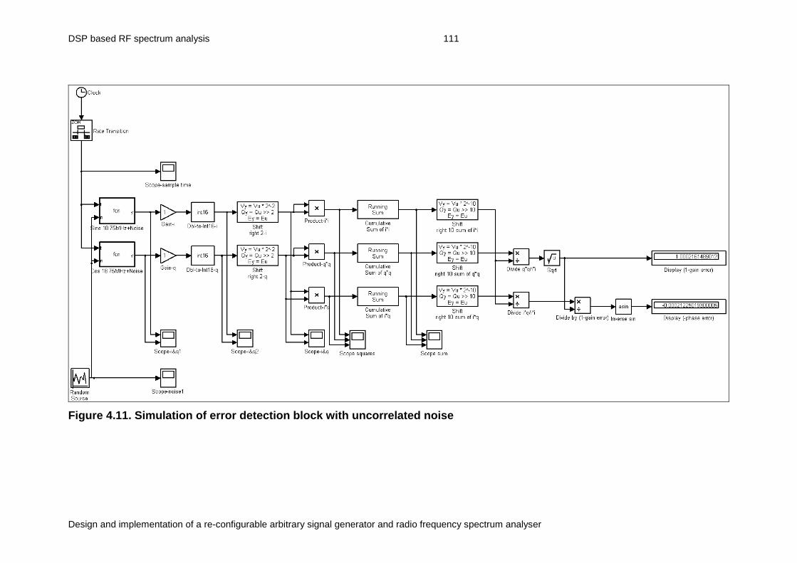
DSP based RF spectrum analysis 111
Design and implementation of a re-configurable arbitrary signal generator and radio frequency spectrum analyser
Figure 4.11. Simulation of error detection block with uncorrelated noise

DSP based RF spectrum analysis 112
Design and implementation of a re-configurable arbitrary signal generator and radio frequency spectrum analyser
The division and square root operations shown in the error detection block are there to
calculate and display gain and phase errors. These operations don’t need to be
performed in the actual hardware implementation. The main aim is to calculate the
multiplying factors 1/(cos()(1-)) and sin()/cos(). It is proved earlier in this chapter
that, 1/(cos()(1-)) is equal to x/(xy-zz)1/2 and sin()/cos() is equal to z/(xy-zz)1/2,
where x, y and z are the three correlation outputs. Therefore, subtraction, inverse
square root and multiplication (or subtraction, square root and division) operations are
needed to be implemented in hardware to calculate the multiplying factors from the
correlation outputs. The actual outputs from the error detection block are shown in
Figure 4.12 below.
DSP based RF spectrum analysis 113
Design and implementation of a re-configurable arbitrary signal generator and radio frequency spectrum analyser
Figure 4.12. Error detection block with multiplying factors as output

DSP based RF spectrum analysis 114
Design and implementation of a re-configurable arbitrary signal generator and radio frequency spectrum analyser
The error compensation block is shown in Figure 4.13 below. Channel Q is multiplied
with 1/(cos()(1-)) (Mult1) and channel I is multiplied with sin()/cos() (Mult2). The
outputs of the multipliers are added together to give QIDEAL. I channel has been
assumed to be ideal. The multiplication and addition operations however will delay
QIDEAL with respect to IIDEAL. Therefore I is multiplied with ‘1’ and Q with ‘0’ and added
together to give IIDEAL. This is purely done to avoid any delays. In the actual design, I
channel will be delayed by the number of clock cycles it takes to perform the
multiplication and addition operations to get QIDEAL.
Figure 4.13. Error compensation block
As mentioned earlier, effect of uncorrelated noise can be minimised by averaging. The
signal to noise ratio was assumed to be 50 dB in which case averaging 1024 samples
was enough to achieve more than 60 dB of image rejection. However, in practice, for
a signal to noise ratio of 36.1 dB, averaging 1024 samples did not achieve the desired
image rejection. Hence further simulations were carried out to evaluate this further.
For signal to noise ration of 36.1 dB, averaging 1024 samples only achieved 54.2 dB
of image rejection. Increasing the number of averaged samples to 2048 did not
improve the image rejection. Averaging 4096 samples improved the image rejection to
56.68 dB. Then as the number of averaged samples are increased there is no

DSP based RF spectrum analysis 115
Design and implementation of a re-configurable arbitrary signal generator and radio frequency spectrum analyser
improvement unless the average samples is increased to 65536 samples where the
image rejection is 57.43 dB.
From this simulation, it was concluded that as the signal to noise ratio deteriorates,
the number of samples that is needed to average will have to increase exponentially in
order to achieve the desired image rejection.
4.13 Simulation of Weaver Architecture
Simulink model of the Weaver architecture is shown in Figure 4.14 below. The
18.75 MHz In-phase and Quadrature inputs are mixed with 25 MHz In-phase and
Quadrature inputs from the local oscillator to produce four different outputs as shown
in the figure. The mixers down converts the 18.75 MHz IF to 6.25 MHz second IF for
further processing.

DSP based RF spectrum analysis 116
Design and implementation of a re-configurable arbitrary signal generator and radio frequency spectrum analyser
Figure 4.14. Simulation of Weaver architecture
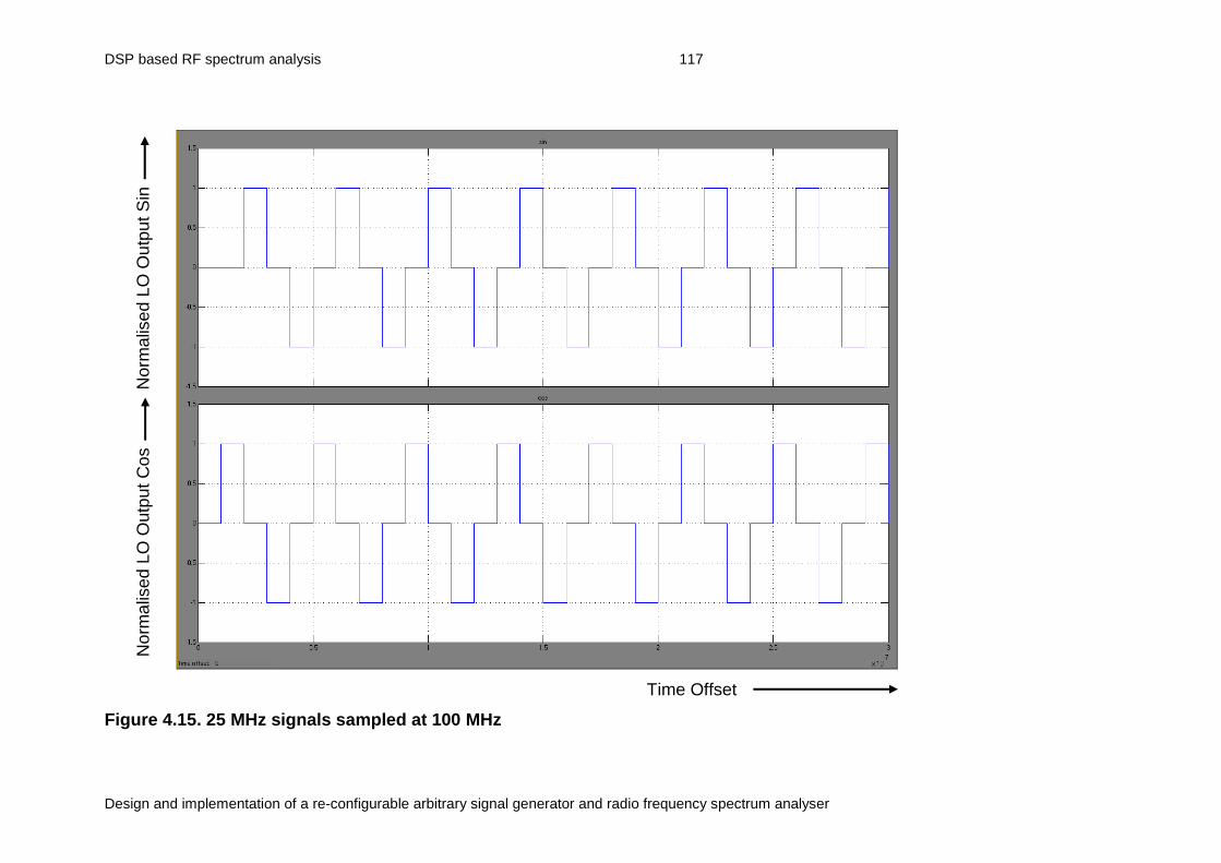
DSP based RF spectrum analysis 117
Design and implementation of a re-configurable arbitrary signal generator and radio frequency spectrum analyser
Time Offset
Figure 4.15. 25 MHz signals sampled at 100 MHz
N
orm
alis
ed
LO
Outp
ut
Co
s
No
rmalis
ed
LO
Ou
tpu
t S
in

DSP based RF spectrum analysis 118
Design and implementation of a re-configurable arbitrary signal generator and radio frequency spectrum analyser
The LO frequency is equal to Fs / 4 where Fs is the sampling rate (100 MHz). The
signal can then be simply generated by repeating the sequence [0, 1, 0, -1]. The 90-
degree phase shifted version is [1, 0, -1, 0] (original sequence delayed by one clock
cycle). The local oscillator waveforms are shown in Figure 4.15 above. The four low-
pass filters are there to remove the 43.25 MHz sum frequency component (25 MHz +
18.25 MHz). Magnitude response of the low-pass filter is shown in Figure 4.16 below.
The filter attenuates the sum (and higher) frequency component by 70 dB.
Figure 4.16. Magnitude response of the filters in the Weaver architecture
The low-pass filter outputs are added and subtracted together to get wanted and
unwanted sidebands. The design was first simulated without any gain or phase error
(simulation time 400 us). The wanted and unwanted I and Q signals are shown in
Figure 4.17 below. The image rejection is about 62.7 dB down.
Then a gain imbalance of 2 % and phase imbalance of 0.1 radians is introduced. The
wanted and unwanted I and Q signals are shown in Figure 4.18 below. In the
presence of imbalances, the image rejection deteriorates to about 26 dB. Therefore,
inputs to the Weaver architecture should be compensated I and Q signals.

DSP based RF spectrum analysis 119
Design and implementation of a re-configurable arbitrary signal generator and radio frequency spectrum analyser
Time Offset
Figure 4.17. Output waveforms without gain or phase error
W
an
ted
IQ
Ou
tpu
t
Unw
an
ted
IQ
Ou
tpu
t
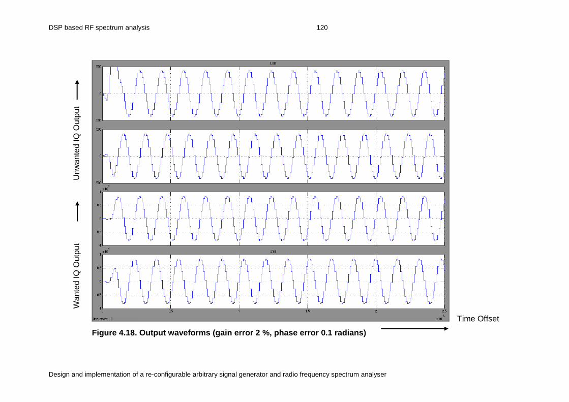
DSP based RF spectrum analysis 120
Design and implementation of a re-configurable arbitrary signal generator and radio frequency spectrum analyser
Time Offset
Figure 4.18. Output waveforms (gain error 2 %, phase error 0.1 radians)
W
an
ted
IQ
Outp
ut
Un
wan
ted
IQ
Outp
ut

DSP based RF spectrum analysis 121
Design and implementation of a re-configurable arbitrary signal generator and radio frequency spectrum analyser
4.14 Simulation of Weaver base-band architecture
Simulink model of the Weaver base-band architecture is shown in Figure 4.19 below.
The 18.75 MHz In-phase and Quadrature inputs are mixed directly down to base-band
with 18.75 MHz In-phase and Quadrature inputs from the local oscillator. The cut-off
frequency of the anti-alias filter for 18.75 MHz IF and 100 MHz sampling rate would
approximately be equal to 40 MHz. A chirp signal source is used to simulate this effect
in the simulation. The frequency is swept from 1 MHz to 41 MHz in 400 us.
The LO frequency is equal to 3 Fs / 16 where Fs is the sampling rate (100 MHz). The
signal can then be simply generated by repeating the sequence [0, 0.9239, 0.7071, -
0.3827, -1, -0.3827, 0.7071, 0.9239, 0, -0.9239, -0.7071, 0.3827, 1, 0.3827, -0.7071
and -0.9239]. The 90-degree phase shifted version is [-1, -0.3827, 0.7071, 0.9239, 0, -
0.9239, -0.7071, 0.3827, 1, 0.3827, -0.7071, -0.9239, 0 0.9239 0.7071 and -0.3827]
(original sequence delayed by four clock cycles).
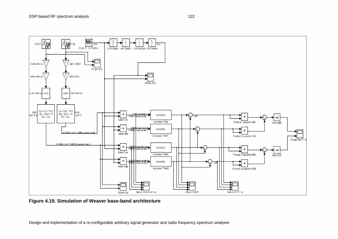
DSP based RF spectrum analysis 122
Design and implementation of a re-configurable arbitrary signal generator and radio frequency spectrum analyser
Figure 4.19. Simulation of Weaver base-band architecture

DSP based RF spectrum analysis 123
Design and implementation of a re-configurable arbitrary signal generator and radio frequency spectrum analyser
The four low-pass filters are narrow-band RBW filters. Magnitude response of the low-
pass filter is shown in Figure 4.20 below.
Figure 4.20. Magnitude response of the resolution bandwidth filters
Amplitude detection is performed on the Upper Side Band (USB) and Lower Side
Band (LSB) signals. The wanted sideband is passed and the unwanted sideband is
attenuated as shown in Figure 4.21 below.

DSP based RF spectrum analysis 124
Design and implementation of a re-configurable arbitrary signal generator and radio frequency spectrum analyser
Figure 4.21. Wanted and image outputs
4.15 Simulation of imbalance computation using Weaver base-band
architecture
It has been proved that the gain and phase imbalance compensation parameters
could be calculated using equations 4.90 and 4.91 as follows.
1/(cos()(1+)) = - ((II x II) + (IQ x IQ)) / ((IQ x QI) – (II x QQ)) (4.90)
sin()/cos() = ((II x QI) + (IQ x QQ)) / ((IQ x QI) – (II x QQ)) (4.91)
where II, IQ, QI and QQ are the four filter outputs in the Weaver base-band
architecture.
This is verified in the simulation shown in Figure 4.22 below.

DSP based RF spectrum analysis 125
Design and implementation of a re-configurable arbitrary signal generator and radio frequency spectrum analyser
Figure 4.22. Simulation of imbalance computation using Weaver base-band architecture

DSP based RF spectrum analysis 126
Design and implementation of a re-configurable arbitrary signal generator and radio frequency spectrum analyser
A gain imbalance of -0.2 and phase imbalance of 22.5 degrees was introduced in one
of the channel of the 18.75 MHz IF. This gives
1/(cos()(1+)) = 1.35299 (4.92)
sin()/cos() = 0.414213 (4.93)
The measured parameters from the simulation were 1.39864 and 0.414952
respectively which closely matches the theoretical result.
4.16 Simulation of IQ imbalance compensation within the IF pass-band
In order to calculate the filter co-efficents of the FIR compensation filter, the gain and
phase imbalance across the IF pass-band is measured. The measured results are
shown in Table 4.1 below. The gain and phase imbalance is only measured up to half
the clock frequency and for the other half the readings are duplicated to form a
conjugate symmetric.
Gain Imbalance
(ratio)
Phase Imbalance (radians)
Normalised Gain
Normalised Phase
Real Imaginary
-1.1493 -0.2718 1.0000 0.0000 1.0000 0.0000
-1.0879 -0.2089 1.0564 -0.0629 1.0543 -0.0664
-1.1076 -0.1823 1.0376 -0.0895 1.0335 -0.0927
-1.1628 -0.2017 0.9884 -0.0701 0.9860 -0.0692
-1.1493 -0.2718 1.0000 0.0000 1.0000 0.0000
-1.0724 -0.2763 1.0717 0.0045 1.0717 0.0048
-1.0567 -0.2329 1.0876 -0.0389 1.0868 -0.0423
-1.0718 -0.2753 1.0723 0.0035 1.0723 0.0038
-1.1493 -0.2718 1.0000 0.0000 1.0000 0.0000
-1.0718 -0.2753 1.0723 0.0035 1.0723 -0.0038
-1.0567 -0.2329 1.0876 -0.0389 1.0868 +0.0423
-1.0724 -0.2763 1.0717 0.0045 1.0717 -0.0048
-1.1493 -0.2718 1.0000 0.0000 1.0000 -0.0000
-1.1628 -0.2017 0.9884 -0.0701 0.9860 0.0692
-1.1076 -0.1823 1.0376 -0.0895 1.0335 0.0927
-1.0879 -0.2089 1.0564 -0.0629 1.0543 0.0664
Table 4.1. Measured gain and phase imbalance across IF pass-band
The gain and phase imbalance is then normalised with respect to the gain and phase
imbalance at the IF frequency (the filter should provide no compensation at IF
frequency as the compensation that is applied at this frequency is correct).

DSP based RF spectrum analysis 127
Design and implementation of a re-configurable arbitrary signal generator and radio frequency spectrum analyser
If G is the normalised gain and P is the normalised phase at the particular frequency ,
then the input to the inverse FFT for that frequency is Xreal + jYreal where
Xreal = ((G x G) / (1 + tan(P) * tan(P)))1/2 (4.94) and Yreal = Xreal x tan(P) (4.95)
Inverse FFT is calculated using the ‘ifft’ function in Matlab. The output of the inverse
FFT is shifted to remove the sharp edges and then used as co-efficients of the FIR
filter defined in Matlab. A window function such as Blackman-Harris window could be
used for further smoothing of the response of the filter. The magnitude and phase
response of the FIR filter are shown in Figure 4.23 and Figure 4.24 below
respectively.
The measured gain and phase imbalance at different frequencies matches the gain
and phase imbalance compensation for the same frequencies provided by the filter.

DSP based RF spectrum analysis 128
Design and implementation of a re-configurable arbitrary signal generator and radio frequency spectrum analyser
Figure 4.23. Magnitude response of the FIR filter

DSP based RF spectrum analysis 129
Design and implementation of a re-configurable arbitrary signal generator and radio frequency spectrum analyser
Figure 4.24. Phase response of the FIR filter

DSP based RF spectrum analysis 130
Design and implementation of a re-configurable arbitrary signal generator and radio frequency spectrum analyser
4.17 Conclusion
This chapter demonstrates the feasibility and functional verification of the spectrum
analyser design. It provided an overview of low IF based image reject architectures
and presented new methods of compensation of imbalances in the RF and IF bands.
The design is simulated in Matlab / Simulink environment and the principles of the
design is validated.
The next chapter details the new design analysis of digital spectrum analyser
architecture with image rejection using Weaver base band architecture and FPGA
design, simulation and synthesis of the new method.

Spectrum analyser – FPGA 131
Design and implementation of a re-configurable arbitrary signal generator and radio frequency spectrum analyser
5 Spectrum Analyser – FPGA Design Simulation and
Synthesis
5.1 Introduction
Certain aspects of the RF architecture outlined in the earlier chapter such as the
frequency limits for the lower and upper RF frequency bands and the final IF for
further digital processing were revised. The block diagram of the final analogue
section is shown in Figure 5.1 below.
Figure 5.1. Analogue section of the RF architecture
The sampling clock frequency was revised down to 40 MHz and the final IF going
into the digital section was chosen to be 10 MHz. The low-pass filters before the ADC
removes the aliasing frequency. The filters attenuate frequencies above 28 MHz by
more than 80 dB. A dual 16-bit ADC digitises the IQ signals for further processing in
the digital domain.
It was initially assumed that a DSP processor would be used for the digital section of
the design. However, it later became clear that it would be quite a challenge to
Spectrum analyser – FPGA 132
Design and implementation of a re-configurable arbitrary signal generator and radio frequency spectrum analyser
implement all the parallel multipliers and filters in a DSP. FPGAs are
characteristically ideal to perform multiple bits multiplication and addition operations
at very high speed and therefore became an obvious choice for implementing the
digital section.
The same family of FPGA used in the generator design was chosen because of
familiarity. The particular FPGA used was Altera Cyclone IV EP4CE40F23C9L.
Choosing an Altera FPGA made the Altera Quartus II design software the most
obvious choice for FPGA design. Altera also provided ModelSim, a comprehensive
simulation and debug environment for FPGA designs. VHDL was predominantly used
to design the spectrum analyser. The Mega Function Wizard of Quartus II was also
used for some specific designs. Filter design software from Matlab were used to
calculate the coefficients of the FIR filter used in the RBW and Video Band Width
(VBW) filter section.
Design analysis and implementations of spectrum analyser sub-systems will be
discussed in this chapter. FPGA implementation of IQ based spectrum analyser
receiver with a novel scheme for image suppression both in the RF and IF pass-band
complete with filtering and detection is an original contribution of this research.
5.2 LVDS Receiver
The outputs from the ADC LTC2191 [74] are serial LVDS. The sampling frequency of
the ADC is 40 MHz. The ADC is configured to output two bits at a time per channel at
320 MHz clock frequency. LVDS receiver shown in Figure 5.2 below is instantiated
using Mega Function Wizard in Quartus to convert the serial LVDS data to parallel.
The ADC also provides the clock to the FPGA.
The input data are in offset binary format and are converted to two’s complement
data by inverting the MSBs of the data inputs in the LVDS decoder block shown in
Figure 5.3 below.

Spectrum analyser – FPGA 133
Design and implementation of a re-configurable arbitrary signal generator and radio frequency spectrum analyser
Figure 5.2. RTL view of the LVDS receiver

Spectrum analyser – FPGA 134
Design and implementation of a re-configurable arbitrary signal generator and radio frequency spectrum analyser
Figure 5.3. RTL view of the LVDS decoder
5.3 IF pass-band imbalance compensation
In order to compensate for imbalance variation within the IF pass-band, a FIR filter is
implemented in one of the channel. The FIR filter is realised in simple direct form as
shown in Figure 5.4 below [72].
Figure 5.4. Direct form realisation of FIR filter

Spectrum analyser – FPGA 135
Design and implementation of a re-configurable arbitrary signal generator and radio frequency spectrum analyser
The number of coefficients in the filter is 32. Therefore, the filter requires 31 delay
registers for each of it input bits, 31 additions, and 32 multiplications. The coefficients
are set by the controlling processor and are stored in the FPGA RAM. The process of
calculating the coefficients has been outlined in the previous chapter.
The other channel is simply delayed by the number of cycles that the filter operation
requires to maintain the phase relationship of the IQ signals.
5.4 RF imbalance compensation
The RF imbalance compensation block is shown in Figure 5.5 below. Channel Q is
multiplied with 1/(cos()(1-)) and channel I is multiplied with sin()/cos(). The
outputs of the multipliers are added together to give QIDEAL. Channel I is simply
delayed by the number of cycles required for the multiplication and addition process.
The parameters 1/(cos()(1-)) and sin()/cos() are computed by the Weaver base-
band method for various frequency bands and stored in the FPGA RAM. The
computation process is explained later in this chapter.

Spectrum analyser – FPGA 136
Design and implementation of a re-configurable arbitrary signal generator and radio frequency spectrum analyser
Figure 5.5. RTL view of RF imbalance compensation

Spectrum analyser – FPGA 137
Design and implementation of a re-configurable arbitrary signal generator and radio frequency spectrum analyser
5.5 Weaver mixers
The I and Q signals free from any imbalances are now converted down to base-band
in the Weaver mixer stage as shown in Figure 5.6 below. The 10 MHz In-phase and
Quadrature Local Oscillator signals are generated in the FPGA using DDS
techniques. The LO frequency is equal to Fs / 4 (10 MHz) where Fs is the sampling
rate (40 MHz). Therefore, it was possible to generate the IQ LOs by simply repeating
the four values [0, 1, 0, -1] and [1, 0, -1, 0] respectively.
However, DDS techniques were used to allow for fine frequency tuning of the LO.
The RF LO step resolution was limited to 1 MHz. The digital LOs provides fine
frequency stepping resolution required for narrow band RBW filters.
The lengths of the accumulators were chosen to be 24 bits which gives 2 uHz
resolution (for 40 MHz clock frequency). 12 MSBs of the accumulators were used to
address the Sin and Cos ROM to generate the quadrature oscillator signals.
The compensated I and Q inputs are multiplied by the I and Q LO outputs to provide
four outputs from the Weaver mixers.

Spectrum analyser – FPGA 138
Design and implementation of a re-configurable arbitrary signal generator and radio frequency spectrum analyser
Figure 5.6. RTL view of Weaver mixers

Spectrum analyser – FPGA 139
Design and implementation of a re-configurable arbitrary signal generator and radio frequency spectrum analyser
5.6 Resolution bandwidth filters
The four identical low-pass filters that follow the mixers remove the sum frequency
components from the mixer outputs. These low-pass filters also function as resolution
band-width filters. The requirement was to implement a wide range of RBW filters
(300 Hz to 3 MHz in 1 – 3 steps). It is not possible to design a digital low-pass filter
with cut-off frequency 150 Hz to get 300 Hz band-width running at 40 MHz. The
resource requirement would have been prohibitively large.
The above problem could be resolved by using CIC filters [8] for decimations,
followed by a FIR filter to provide the filter shape as shown in Figure 5.7 below [75].
Figure 5.7. RTL view of RBW filters
The solution was to use CIC filters for decimations, followed by a FIR filter to provide
the filter shape at each of the mixer outputs. The low-pass FIR filter was designed
with cut-off frequency 1.5 MHz for 3 MHz bandwidth at 40 MHz clock frequency. The
other bandwidths were simply achieved by decimating the clock frequency using CIC
filters. A fifth order CIC filter of differential delay two was found to be sufficient for all
the required decimation rates. The bit growth for the narrowest RBW is 72 bits. The
mixer outputs are 16 bits long. Therefore, the additions and subtractions in the CIC
filters are carried out in 88 bits. Owing to the large number of bits, the additions and
subtractions operations are pipelined. The output of the CIC filters are truncated to
16 bits before being used as inputs to the FIR filters.
Table 5.1 below provides clock frequency, rate change and bit growth for various
RBW filters used in the design.
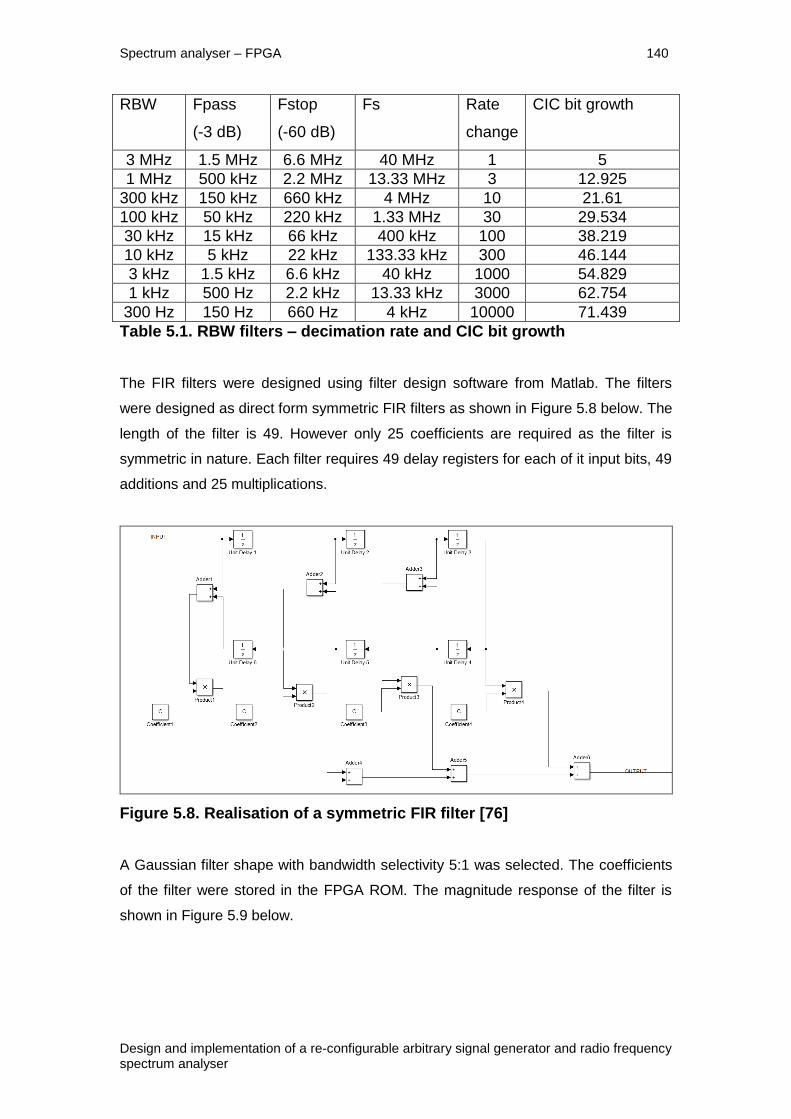
Spectrum analyser – FPGA 140
Design and implementation of a re-configurable arbitrary signal generator and radio frequency spectrum analyser
RBW Fpass
(-3 dB)
Fstop
(-60 dB)
Fs Rate
change
CIC bit growth
3 MHz 1.5 MHz 6.6 MHz 40 MHz 1 5
1 MHz 500 kHz 2.2 MHz 13.33 MHz 3 12.925
300 kHz 150 kHz 660 kHz 4 MHz 10 21.61
100 kHz 50 kHz 220 kHz 1.33 MHz 30 29.534
30 kHz 15 kHz 66 kHz 400 kHz 100 38.219
10 kHz 5 kHz 22 kHz 133.33 kHz 300 46.144
3 kHz 1.5 kHz 6.6 kHz 40 kHz 1000 54.829
1 kHz 500 Hz 2.2 kHz 13.33 kHz 3000 62.754
300 Hz 150 Hz 660 Hz 4 kHz 10000 71.439
Table 5.1. RBW filters – decimation rate and CIC bit growth
The FIR filters were designed using filter design software from Matlab. The filters
were designed as direct form symmetric FIR filters as shown in Figure 5.8 below. The
length of the filter is 49. However only 25 coefficients are required as the filter is
symmetric in nature. Each filter requires 49 delay registers for each of it input bits, 49
additions and 25 multiplications.
Figure 5.8. Realisation of a symmetric FIR filter [76]
A Gaussian filter shape with bandwidth selectivity 5:1 was selected. The coefficients
of the filter were stored in the FPGA ROM. The magnitude response of the filter is
shown in Figure 5.9 below.
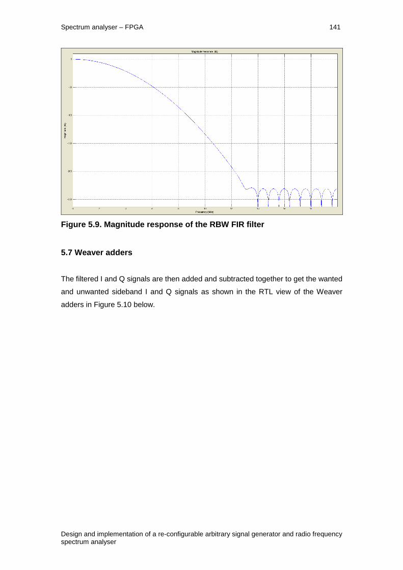
Spectrum analyser – FPGA 141
Design and implementation of a re-configurable arbitrary signal generator and radio frequency spectrum analyser
Figure 5.9. Magnitude response of the RBW FIR filter
5.7 Weaver adders
The filtered I and Q signals are then added and subtracted together to get the wanted
and unwanted sideband I and Q signals as shown in the RTL view of the Weaver
adders in Figure 5.10 below.

Spectrum analyser – FPGA 142
Design and implementation of a re-configurable arbitrary signal generator and radio frequency spectrum analyser
Figure 5.10. RTL view of the Weaver adders

Spectrum analyser – FPGA 143
Design and implementation of a re-configurable arbitrary signal generator and radio frequency spectrum analyser
5.8 Amplitude detector
After resolution bandwidth filtering, the I and Q signals are squared and added and
the square root of the results gives the amplitude of the signal [77]. Dedicated
multipliers embedded in the FPGA are used to perform squaring of I and Q signals. It
was also possible to perform 32-bit addition in one 40 MHz clock cycle.
Implementing square root function in FPGA is not straight forward and requires a lot
of hardware [79]. The I and Q signals are 16 bits long where the signal value only
occupies 15 bits as the Weaver adder blocks halves the signal. The multiplication
output is 32 bits long. The addition should add one more bit. However, as the signal
value was only 15 bits to start with, there is no need to add a bit. The square root
operation results in a 16-bit output. Square root implementation is based on non-
restoring square root algorithm [89]. Starting from the MSB, a count of one is
subtracted from every pair of bits. The sign of the result determines the quotient bit
and the remainder is added or subtracted to the next pair of bits based on the sign of
the previous result. This process is repeated for every pair of bits down to LSB. The
quotient is the desired result. For calculating the square root of a 32-bit number, 16
iterations are required which results in 32 pipeline stages.
5.9 Video bandwidth filters
A VBW filter is a low-pass filter that comes after amplitude detection that determines
the bandwidth of the video signal [5].
A similar structure to the RBW filter is used to implement the wide range of VBW
filters as well. A fifth order CIC filter is used to provide all the required decimation
rates and a FIR filter designed using Matlab filter design software is used to provide
low-pass filtering.
5.10 Demodulation
The availability of I and Q base-band signals makes signal demodulation analysis
quite straight forward [78].

Spectrum analyser – FPGA 144
Design and implementation of a re-configurable arbitrary signal generator and radio frequency spectrum analyser
Amplitude modulation can be extracted from I and Q by taking the square root of the
sum of the squares of I and Q [78]. In other words, the output from the amplitude
detector is the AM demodulated output as well.
The instantaneous phase of the modulated signal is the result of the derivative of the
arctangent of Q divided by I [78]. Division requires a lot of hardware. Inverse
operation could be performed by storing the values of the inverse of a signal in a
ROM. The rate of change of phase will result in FM modulating signal. The rate of
change is simply the subtraction of two consecutive phase samples. If subtraction is
performed after inverse operation, then two ROMs are required. This is not ideal.
Therefore, instead of dividing Q by I, (IcurrentQnext - QcurrentInext) is divided by (QcurrentQnext
- IcurrentInext) which gives tangent of the difference of two consecutive phase samples.
The inverse will result in FM demodulated output.
Dedicated embedded multipliers are used for the multiplication of Icurrent and Qnext,
Qcurrent and Inext, Qcurrent and Qnext, and Icurrent and Inext. The results are 32-bit long. It was
possible to perform 32 bit subtractions in one 40 MHz clock cycle. The ROM holds
1024 samples of the inverse function. Therefore, the divider needs to output 10-bit
result which is used as an address to the ROM. Division of a 32-bit number, by a 32-
bit number to output 10 bits requires a lot of hardware. The divider implementation is
based on non-restoring division algorithm [90]. The denominator is subtracted from
the numerator. The sign of the result determines the quotient bit and the denominator
is added or subtracted to the result based on the sign of the previous result. This
process is repeated for the number of desired bits in the result. For a 10-bit result, 10
pipeline stages are necessary.
5.11 RF Imbalance computation block
This imbalance compensation block shown in Figure 5.11 below calculates the gain
and phase imbalance compensation parameters used in the RF compensation block
using equations 4.90 and 4.91 as follows.
1/(cos()(1+)) = - ((II x II) + (IQ x IQ)) / ((IQ x QI) – (II x QQ)) (4.90)
sin()/cos() = ((II x QI) + (IQ x QQ)) / ((IQ x QI) – (II x QQ)) (4.91) 4.91
where II, IQ, QI and QQ are the four resolution bandwidth filter outputs.
Spectrum analyser – FPGA 145
Design and implementation of a re-configurable arbitrary signal generator and radio frequency spectrum analyser
As mentioned before, the division functions require a lot of hardware to be
implemented in the FPGA.
During the computation process, normal acquisition is halted and an internal
calibration signal is routed to the FPGA. The input level of the calibration signal is
very close to the maximum input amplitude to the ADC to achieve maximum image
rejection. No digital compensation is applied to this input signal and is passed to the
Weaver architecture where compensation parameters are computed. Some
averaging is performed before the calculation to further reduce the noise for more
accurate results. The computed values are stored in the FPGA RAM for future use.
Since the imbalance is not the same for all input frequencies, the entire frequency
band is sub-divided and calibration is performed for each sub-band. The process is
repeated periodically to account for the drifts in the gain and phase imbalance with
temperature and therefore maximum image rejection is maintained at all times.

Spectrum analyser – FPGA 146
Design and implementation of a re-configurable arbitrary signal generator and radio frequency spectrum analyser
Figure 5.11. RTL view of the imbalance computation block

Spectrum analyser – FPGA 147
Design and implementation of a re-configurable arbitrary signal generator and radio frequency spectrum analyser
5.12 FPGA Synthesis
The previous section charts the design considerations and implementation of the
spectrum analyser design. Once the design was verified, it was synthesized using
Quartus II in a Cyclone IV FPGA (EP4CE40F23C9L). The summary of synthesis is
presented in Table 5.2 below.
Following synthesis, the design was fitted in the FPGA. The design was analysed to
check whether it meets the timing requirements. Finally, programming files were
generated to allow programming or configuration of the device. All of these
procedures were performed by the Quartus II software tool provided by Altera.
Flow Status Successful - Wed May 07 15:23:44 2014
Quartus II Version 13.1 Build 163 10/23/2013 SJ Web
Edition
Revision Name PSA6005_Spectrum_Analyser_Top_Level
Top-level Entity Name PSA6005_Spectrum_Analyser_Top_Level
Family Cyclone IV E
Device EP4CE40F23C9L
Timing Models Final
Met timing requirements Yes
Total logic elements 39,126 / 39,600 ( 99 % )
Total combinational functions 31,270 / 39,600 ( 79 % )
Dedicated logic registers 26,660 / 39,600 ( 67 % )
Total registers 26668
Total pins 74 / 329 ( 22 % )
Total virtual pins 0
Total memory bits 896,672 / 1,161,216 ( 77 % )
Embedded Multiplier 9-bit elements 232 / 232 ( 100 % )
Total PLLs 1 / 4 ( 25 % )
Table 5.2. Quartus flow summary for the spectrum analyser project
The design was also analysed to find out how much power it will consume using
‘Power Play Power Analyzer Tool’ in Quartus II. The results were then passed on to
the analogue design engineer in the company for power supply designs.

Spectrum analyser – FPGA 148
Design and implementation of a re-configurable arbitrary signal generator and radio frequency spectrum analyser
A schematic was then prepared for the FPGA. Input and output signals were
assigned to various pins in the FPGA as shown in Figure 5.12 below. Synthesis was
carried out again to check the validity of the assignments.
Figure 5.12. FPGA pin assignment – top level view
Schematic was prepared so that the FPGA can be configured in JTAG programming
mode using ‘Altera USB Blaster’ during the development stages and in Active Serial
(AS) programming mode using serial configuration device during production. The
schematic was prepared using configuration application note [80] provided by Altera.
Finally, FPGA interface to ADC, micro controller, and other analogue hardware were
finalised. Figure 5.13 below shows the interface between the FPGA and the ADC.
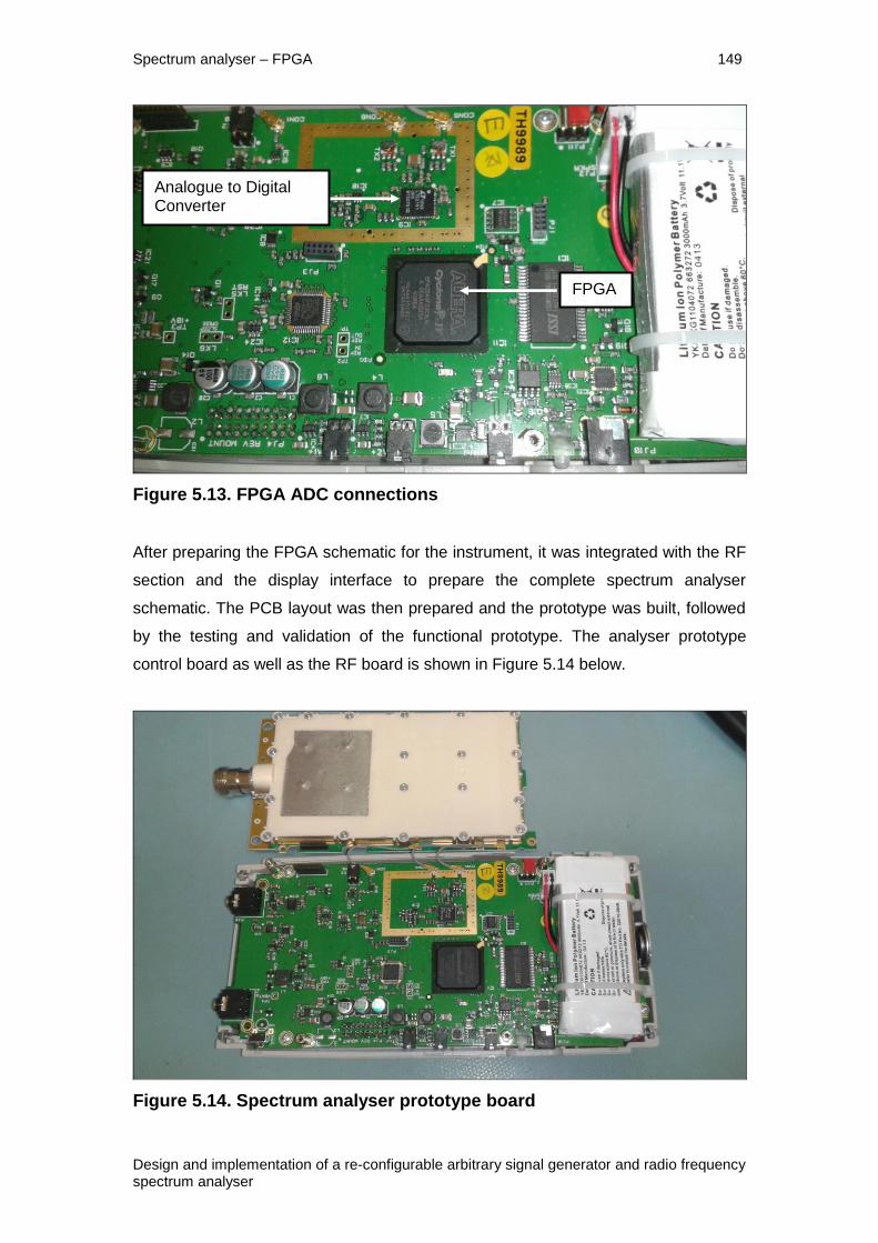
Spectrum analyser – FPGA 149
Design and implementation of a re-configurable arbitrary signal generator and radio frequency spectrum analyser
Figure 5.13. FPGA ADC connections
After preparing the FPGA schematic for the instrument, it was integrated with the RF
section and the display interface to prepare the complete spectrum analyser
schematic. The PCB layout was then prepared and the prototype was built, followed
by the testing and validation of the functional prototype. The analyser prototype
control board as well as the RF board is shown in Figure 5.14 below.
Figure 5.14. Spectrum analyser prototype board
Analogue to Digital Converter
FPGA
Spectrum analyser – FPGA 150
Design and implementation of a re-configurable arbitrary signal generator and radio frequency spectrum analyser
5.13 Results
The spectrum analyser is in itself a measurement receiver. Therefore, the displayed
output provides functional verification of the design. The results presented in this
section are screen shots of the actual finished and working spectrum analyser. In the
complete unit, measurement sweep is controlled by the controlling processor
whereas measurement and sweep detection is done by the FPGA receiver. The
control processor then passes on the sweep data to the display processor via
Universal Asynchronous Receiver Transmitter (UART) interface. The display
processor then displays the measurement on a Thin Film Transistor (TFT) Liquid
Crystal Display (LCD). An RF generator was used to provide signal input to the
analyser.
The signal input frequency was chosen to be 1 GHz. The spectrum analyser was
programmed to perform a sweep with centre frequency 1 GHz and frequency span of
5 MHz. The frequency range falls in the lower RF frequency band of the architecture.
The first RF LO is swept from 4405 MHz to 4415 MHz. The sum frequency is filtered
out and the difference frequency is passed to the second RF LO which is fixed at
3410 MHz. The second RF LO down converts the frequency to 10 MHz final
analogue IF which is then digitised for further processing.

Spectrum analyser – FPGA 151
Design and implementation of a re-configurable arbitrary signal generator and radio frequency spectrum analyser
Figure 5.15. Spectrum of 1 GHz signal input
The RF LO is stepped in 1 MHz steps. The digital LO is stepped in finer resolution.
The stepping resolution is RBW dependent. For 100 kHz RBW, the digital LO is
stepped in 33 kHz steps.
Figure 5.15 above shows the spectrum result. The result shows that the analyser is
capable of displaying the input waveform. The result validates the amplitude
accuracy, resolution bandwidth selectivity and noise floor performance specification
of the analyser. RBW and VBW filters were set to 100 kHz. The Gaussian shape of
the RBW filter can be clearly seen in the spectrum.

Spectrum analyser – FPGA 152
Design and implementation of a re-configurable arbitrary signal generator and radio frequency spectrum analyser
Figure 5.16. Spectrum of 1 GHz signal input for wide RBW setting
Figure 5.16 above shows the spectrum result for a wider RBW filter setting of 1 MHz.
Span is increased to 20 MHz to show the full filter shape. The signal to noise ratio is
approximately 10 dB worse than it was for a 100 kHz RBW which is expected. A
wider filter will allow more noise to pass through. The filter shape hasn’t changed
because it uses the same FIR filter. This result is presented to show that the RBW is
a selectable parameter. RBW can be changed from 10 MHz to 300 Hz in 1 – 3 steps.
Figure 5.17 below shows the spectrum result for a narrower RBW filter setting of
10 kHz. Span is decreased to 1 MHz to present a clear spectrum. The noise floor has
gone down as expected. But the noise on the skirts of the filter has increased. This is
due to the limited phase noise performance of the RF local oscillators. The phase
noise of the local oscillators is specified as -83.5 dBc/Hz at 10 kHz offset which is not
very good. The filter follows the Gaussian shape down to about 50 dB from reference
before it hits the noise floor of the oscillators. The shape then becomes horizontal up
to the cut-off frequency of the PLL loop filter bandwidth when it starts to decrease
again.

Spectrum analyser – FPGA 153
Design and implementation of a re-configurable arbitrary signal generator and radio frequency spectrum analyser
Figure 5.17. Spectrum of 1 GHz signal input for narrow RBW setting
Figure 5.18 below shows the spectrum result for 100 kHz RBW and 1 kHz VBW. As
expected, a narrow video bandwidth filter removes more noise from the spectrum
output. The effect is similar to averaging. This result validates the functional
verification of the video bandwidth filter performance of the analyser. The video
bandwidth filter can be changed from 10 MHz to 300 Hz in 1 – 3 steps.

Spectrum analyser – FPGA 154
Design and implementation of a re-configurable arbitrary signal generator and radio frequency spectrum analyser
Figure 5.18. Spectrum of 1 GHz signal input for narrow VBW setting
The signal input is then frequency modulated with 1 kHz sine wave and frequency
deviation of 100 kHz. The spectrum result is shown in Figure 5.19 below. The
following two results validate the frequency demodulation specification of the
spectrum analyser.

Spectrum analyser – FPGA 155
Design and implementation of a re-configurable arbitrary signal generator and radio frequency spectrum analyser
Figure 5.19. Spectrum of FM modulated 1 GHz signal input
Figure 5.20 below shows the demodulated waveform. The x-axis is time axis which
clearly shows the modulation frequency to be 1 kHz. The y-axis is the deviation axis.
The deviation is 100 kHz in either direction. The RBW setting has to be wider than
the frequency of the modulating waveform and frequency deviation to perform
demodulation.

Spectrum analyser – FPGA 156
Design and implementation of a re-configurable arbitrary signal generator and radio frequency spectrum analyser
Figure 5.20. FM Demodulated waveform
The signal input is then amplitude modulated with 1 kHz sine wave with depth set to
50 %. Figure 5.21 below shows the demodulated waveform. This result validates the
amplitude demodulation specification of the spectrum analyser. The x-axis is time
axis which clearly shows the modulation frequency to be 1 kHz. The y-axis is the
depth axis. The depth is 50 % in either direction. The RBW setting has to be wider
than the frequency of the modulating waveform to perform demodulation.
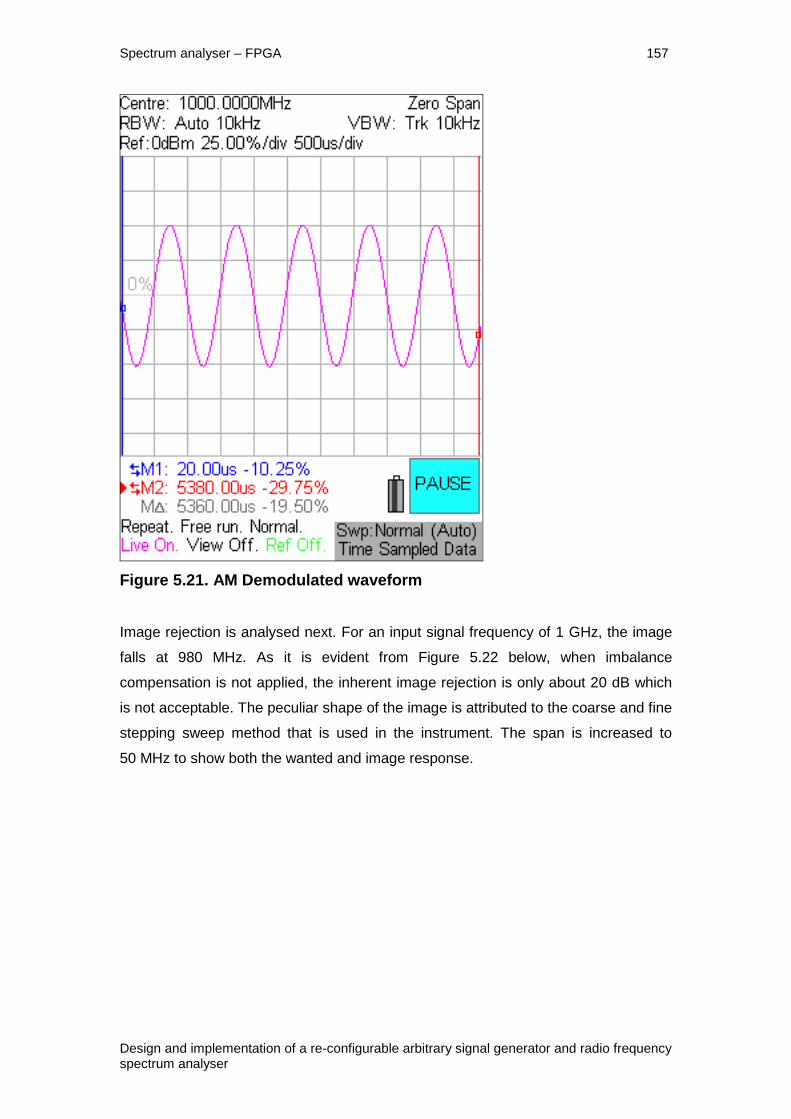
Spectrum analyser – FPGA 157
Design and implementation of a re-configurable arbitrary signal generator and radio frequency spectrum analyser
Figure 5.21. AM Demodulated waveform
Image rejection is analysed next. For an input signal frequency of 1 GHz, the image
falls at 980 MHz. As it is evident from Figure 5.22 below, when imbalance
compensation is not applied, the inherent image rejection is only about 20 dB which
is not acceptable. The peculiar shape of the image is attributed to the coarse and fine
stepping sweep method that is used in the instrument. The span is increased to
50 MHz to show both the wanted and image response.

Spectrum analyser – FPGA 158
Design and implementation of a re-configurable arbitrary signal generator and radio frequency spectrum analyser
Figure 5.22. Image rejection when compensation is not applied
When the gain and phase imbalance is compensated, the image rejection improves
drastically as shown in Figure 5.23 below. For the same setting, the image is
suppressed down to the noise floor when compensation is applied. It is possible to
achieve 60 dB of image rejection over the entire input frequency range using the
compensation method.

Spectrum analyser – FPGA 159
Design and implementation of a re-configurable arbitrary signal generator and radio frequency spectrum analyser
Figure 5.23. Image rejection when compensation is applied
The RF compensation only achieves maximum image rejection at one point in the IF
filter pass-band. Therefore, compensation is required for imbalance variation within
the IF pass-band. This is demonstrated in Figure 5.24 and Figure 5.25 below.
Span is reduced to only concentrate on the image response. A wider RBW is used as
the effect is more evident for wide RBWs. Figure 5.24 below shows the image
response when IF pass-band compensation is not applied.

Spectrum analyser – FPGA 160
Design and implementation of a re-configurable arbitrary signal generator and radio frequency spectrum analyser
Figure 5.24. Image rejection when IF pass-band compensation is not
applied
The image rejection is maximum at IF. However away from the IF, the image
rejection deteriorates.
Figure 5.25 below shows the image rejection when IF pass-band compensation is
applied.

Spectrum analyser – FPGA 161
Design and implementation of a re-configurable arbitrary signal generator and radio frequency spectrum analyser
Figure 5.25. Image rejection when IF pass-band compensation is applied
When IF pass-band compensation is applied, the image disappears.
5.14 Conclusion
This chapter concludes the FPGA design for the digital spectrum analyser. Results
presented validate the specifications of the spectrum analyser design.

Conclusions 162
Design and implementation of a re-configurable arbitrary signal generator and radio frequency spectrum analyser
6 Conclusions and Future Work
Signal generators and spectrum analysers or signal receivers are probably the two
most important instruments used in test and measurement applications. Recent
availability of high performance and low cost FPGAs opens up the possibilities to
design customised solutions for these instruments in a single chip.
This research has demonstrated the implementation of an entirely digital and
modular, system on chip design of a versatile signal waveform generator in a generic
FPGA. This thesis has provided a detailed overview of the principles behind the
designs as well as simulation, functional verification and implementation of the
concepts. The end result is a high-end generator with comprehensive modulation
capabilities. This research has also developed a complete system on chip radio
frequency spectrum analyser based on digital signal processing. IQ image reject
mixers were tailored for application in a wide band system using novel techniques.
The result presented in the previous chapter validates the new design. The two
designs are completely portable and therefore find use in any generic digital platform.
The objectives of the two designs were met and exceeded. The performances were
assessed, and the specification enhanced, as the project proceeded. The final
instruments comfortably exceeded the original target specification and outclassed the
major competitors at its price-point. The benefit of the better specification was that it
was also possible to offer lower cost products with a lower specification limited in
software in order to cover a broader section of the market than originally proposed.
Waveform frequency specification of 50 MHz was achieved. The generator included
16 standard waveforms in addition to pulse, noise and user-defined arbitrary
waveforms. Minimum edge time of 5 ns was achieved in pulse waveforms with pulse
timing parameters resolution of 100 ps. The generator achieved low jitter
asynchronous operation for externally triggered pulses. The design also incorporated
comprehensive modulation capabilities including AM, FM, PM, FSK, BPSK, SUM,
PWM and PDM.
The spectrum analyser achieved wide frequency range from 10 MHz to 6000 MHz
to 100 Hz resolution. A wide range of RBW and VBW filters between 300 Hz and
10 MHz were implemented. The instrument achieved a dynamic range of 84 dB,

Conclusions 163
Design and implementation of a re-configurable arbitrary signal generator and radio frequency spectrum analyser
displayed average noise floor less than -120 dB with -40 dB reference level and a
typical specification of 60 dB of image rejection over the entire frequency range.
Amplitude accuracy and linearity specification was better than +/- 1 dB.
As with any design, further optimisations are possible. Modern modulation schemes
such as Quadrature Amplitude Modulation, Orthogonal Frequency Division
Multiplexing, Quadrature Phase Shift Keying and IQ modulation are all possible in a
DDS system but were not included in this research. Future works could include the
possibility of adding digital modulation schemes to the generator. The possibility of
modifying the white noise generator to output noise with user defined distribution was
briefly discussed in chapter 3. The RAM in the FPGA holds the user defined
distribution. The development of memory algorithms to produce various standard
distributions used in test and measurement applications will require some effort. The
drawbacks of using DDS techniques to generate arbitrary waveforms were
highlighted in chapter 2 and 3. It should be possible to overcome some of these
limitations. The idea of an arbitrary waveform generator is to repeat the same points
stored in the RAM on every cycle of the waveform. The accumulator overflow error in
the DDS prohibits it from doing so. However, this error is completely deterministic. It
should be possible to use this information to possibly delay the RAM address by
using some sort of a fractional delay FIR filter. If this solution is feasible then it would
be possible to develop an arbitrary waveform generator which does not suffer from
DDS distortions. Additionally, since the solution will still essentially be DDS based, it
would be very easy to add frequency and phase modulation which is not possible, or
very difficult to implement in a conventional arbitrary waveform generator. Further
development time could be invested to determine the feasibility of such a solution.
The clock frequency of the DDS based generator limits the maximum output
frequency. The maximum clock frequency of a fairly complex digital generator design
in a low cost FPGA is 200 MHz. This limits the output frequency to about 80 MHz for
a sinusoidal waveform. The limits for an arbitrary waveform is even less. However,
most low-cost FPGAs feature IO interfaces that could run at four times the maximum
clock frequency. Therefore, it should be possible to implement a four generator
solution. Each of the generators could run at the clock frequency where their initial
phases are shifted with respect to one another. The outputs of the four generators
could then be multiplexed and sent to the DAC at four times the clock rate. The
maximum frequency of the resultant waveform could then be 320 MHz. There are a
Conclusions 164
Design and implementation of a re-configurable arbitrary signal generator and radio frequency spectrum analyser
lot of things to consider here. The resource usage in the FPGA would increase
considerably and the design might not fit in the same FPGA and a bigger FPGA
might be required. If modulation capabilities are required in such a design, then four
such modulation generators would be needed. More research is needed to prove
whether this solution would work.
The analyser project used two DDS based generators in its receiver architecture and
therefore proved another application for the generator design. The model could also
be used in a modulator rather than a demodulator where generator could produce the
In-phase and Quadrature signals with great amplitude and phase accuracy. It is also
possible to use the generator design concept in a RF generator application where the
DDS based generator could be used to generate the reference frequency used in the
RF PLL. Analogue and digital FM could be achieved by modulating the DDS
reference. AM could be achieved with a PIN diode circuit in the RF path. In order to
frequency modulate the reference, the PLL loop bandwidth needs to be quite wide
which might make the delta sigma noise quite excessive. Further investigation is
needed.
Having successfully designed a low-cost spectrum analyser, the next obvious step
forward is to boost its performance by developing and including in it real-time
spectrum analysis capabilities. Most of the research on real time spectrum analysers
is focussed on real time signal processing using FFT. It is assumed that images or
spurious responses are removed by preceding hardware filters. The need of tuneable
low-pass image reject filters makes the design quite bulky and therefore makes it
difficult to develop a portable hand-held solution.
The linear nature of the image rejection suppression algorithm developed for the
analyser design makes it suitable for transient signal analysis. However regular
internal alignment is needed which interrupts the normal sweep operation which
might not be acceptable in a real time operation. Future research could concentrate
in applying modifications to the existing design such that imbalances are computed
using the input signal rather than a separate calibration signal source [73] [85]. In the
absence of sufficient input signal, the algorithm would stop and would continue to use
the current value until a sufficiently large is detected. If there is no input or a small
input, then the image rejection does not need to be good anyway. The compensated
I and Q signals could then be used for further FFT processing. Future work is needed

Conclusions 165
Design and implementation of a re-configurable arbitrary signal generator and radio frequency spectrum analyser
in this area to determine the portability of the spectrum analyser design for a real
time application.
Last but not least, the spectrum analyser design could be used in a modulator design
in a RF generator application where the base band I and Q signals are mixed with RF
I and Q LO signals and then added together to generate the RF output. The
modulator enables the possibility of implementing complex modulation schemes in
the RF generator. However, the base band I and Q needs to be free of gain and
phase imbalance over the entire RF output range to achieve sufficient side bands
suppression. The digital I and Q signals are ideal and imbalances are introduced at
the mixer stages. A feedback from the output of the mixer is needed to calculate and
compensate for the imbalances. The same theory of imbalance computation and
correction could still be used, but the application of compensation will have to be
done retrospectively [92]. Future work could concentrate on the feasibility of this
design.
This chapter concludes the research and road map ahead has been briefly
presented.

References 166
Design and implementation of a re-configurable arbitrary signal generator and radio frequency spectrum analyser
References
[1] Tierney J, “A digital frequency synthesizer”, IEEE Transactions on Audio and
Electroacoustics, 19 August 1971, Volume No. 1, Pages 48 – 57.
[2] Larson D.C, “High Speed Direct Digital Synthesis Techniques and Applications”,
20th Annual Gallium Arsenide Integrated Circuit Symposium, 1-4 November 1998,
Technical Digest, Pages 209-212.
[3] Vanka J & Halonen K, “Direct Digital Synthesizers, Theory, Design and
Applications”, ISBN 0-7923-7366-9, Kluwer Academic Publishers, 2001.
[4] New to FPGAs Resource Center – Altera, available:
http://www.altera.co.uk/devices/fpga/new-to-fpgas/resource-center.html [accessed
16/01/2015].
[5] “Agilent Spectrum Analysis Basics”, Agilent Application Note 150 New Edition,
August 2, 2006.
[6] Earls J.D., “Use of a pre-selection filter bank and switched local oscillator counter
in an instrumentation receiver”, US Patent 7702305 B2, April 20, 2010.
[7] Rovers K.C., “Front-end research for a low-cost spectrum analyser – receiver
system and topology study”, available:
http://essay.utwente.nl/57291/1/scriptie_Rovers.pdf [accessed 12/06/2010].
[8] Hogenauer E.B., “An economical class of digital filters for decimation and
interpolation”, IEEE Transactions on Acoustics, Speech and Signal Processing, April
1981, Vol. 2, 29.
[9] Soudris D, Kesoulis M, Koukourlis C, Thanailakis A & Blionas S, “Alternative
Direct Digital Frequency Synthesizer Architectures with Reduced Memory Size”,
Proceedings of the International Symposium on Circuits and Systems, 25 – 28 May
2003, Volume 2, Pages 73 – 76.

References 167
Design and implementation of a re-configurable arbitrary signal generator and radio frequency spectrum analyser
[10] Goldberg, Bar-Giora, “Digital Frequency Synthesis Demystified”, LLH
Technology Publishing, 1999.
[11] Hutchinson B.H., “Frequency Synthesis and Applications”, IEEE Press, 1975.
[12] Park M, Kim K and Lee J.A., “CORDIC-Based Direct Digital Synthesizer:
Comparison with a ROM-Based Architecture in FPGA Implementation”, IEICE Trans.
Fundam., Volume E83-A, No. 6, June 2000.
[13] McCune Junior E.W., “Number Controlled Modulated Oscillator”, US Patent
4746880, May 24, 1988.
[14] “Direct Digital Synthesis (DDS) using FPGA”, Hunt Engineering – user support,
available: http://www.hunteng.co.uk/support/dds.htm [accessed 07/11/2007].
[15] Song Y, Liang H, Zhou L, Du J, Ma J and Yue Z., “Large Dynamic Range High
Resolution Digital Delay Generator Based on FPGA”, Conference on Electronics,
Communications and Control, 9-11 September 2011, Pages 2116 – 2118.
[16] Sullivan S.K, Veith R.L, Akiyama I , Fujisawa Y & Aizawa Y., “Triggered DDS
Pulse Generator Architecture”, US Patent US7281025 B2, October 9, 2007.
[17] Kalisz J., “Review of methods for time interval measurements with picoseconds
resolution”, Metrologis, volume 41, pp. 17 – 32, 2004.
[18] “Altera Cyclone IV Device Datasheet”, available:
http://www.altera.co.uk/literature/hb/cyclone-iv/cyiv-53001.pdf [accessed
20/01/2015].
[19] “Xilinx Spartan – 6 Family Overview”, available:
http://www.xilinx.com/support/documentation/data_sheets/ds160.pdf [accessed
20/01/2015].
[20] Wu J, Shi Z, Wang I.Y., “Firmware-only Implementation of Time-to-Digital
Converter (TDC) in Field-Programmable Gate Array (FPGA)”, Nuclear Science
Symposium Conference Record, IEEE 19 – 25 October 2003, Volume 1, Pages 19 –
25.

References 168
Design and implementation of a re-configurable arbitrary signal generator and radio frequency spectrum analyser
[21] Uusikartano R, Niittylahti J & Renfors M, “Area-Optimized FPGA Implementation
of a Digital FM Modulator”, Proceedings of the 1999 IEEE International Symposium
on Circuits and Systems, July 1999, Volume 4, Pages 360-362.
[22] “Altera CIC MegaCore Function User Guide”, available:
http://www.altera.co.uk/literature/ug/ug_cic.pdf [accessed 20/01/2015].
[23] “Understanding Signal Generation Methodologies”, available:
http://www2.tek.com/cmsreplive/tirep/4477/2006.09.20.08.10.50_4477_EN.pdf
[accessed 15/11/2007].
[24] Sullivan S.K, Veith R.L, Akiyama I & Fujisawa Y, “DDS Pulse Generator
Architecture”, US Patent US2005/0134330A1, June 23, 2005.
[25] Dobramysl D, Hofmann L & Lillie F, “Clock Signal Generator Employing a DDS
Circuit”, US Patent US6642754B1, November 4, 2003.
[26] Agilent 33220A user’s guide, Publication Number 33220-90002, Edition 3, March
2005.
[27] Chu P.P & Jones R.E, “Design techniques of FPGA based random number
generator”, Proceedings of Military and Aerospace Applications of Programmable
Devices and Techniques Conference, 1999.
[28] Ionescu F.C, “Theory and Practice of a Fully Controllable White Noise
Generator”, International Semi-Conductor Conference, Romania, 9-12 October 1996,
Volume 2, Pages 319-322.
[29] Napier T.M, “Digital Gaussian White Noise Generation System and Method of
Use”, US Patent 5057795, October 15, 1991.
[30] O’Brien J, Gaffney B & Liu B, “A High Speed Digital Noise Generator”, South-
East Conference Proceedings, 5-8 April 1981, Pages 558 – 560.
[31] Danger J.L, Ghazel A, Boutillon E & Laamari H, “Efficient FPGA implementation
of Gaussian noise generator for communication channel emulation”, Proceedings of

References 169
Design and implementation of a re-configurable arbitrary signal generator and radio frequency spectrum analyser
the 7th IEEE International Conference on Electronics, Circuits and Systems 2000,
Volume 1, Pages 366-369.
[32] Ghazel A, Boutillon E, Danger J.L, Gulak G & Laamari H, “Design and
performance analysis of a high speed AWGN communication channel emulator”,
Proceedings of the IEEE Pacific Rim Conference on Communications, Computers
and Signal Processing, Volume 2, Pages 374–377.
[33] Lee D, Luk W, Villasenor J & Cheung P.Y.K, “A Hardware Gaussian Noise
Generator for Channel Code Evaluation”, 11th Annual IEEE Symposium on Field-
Programmable Custom Computing Machines, 2003, 9-11 April 2003, Pages 69 – 78.
[34] Fung E, Leung K, Parimi N, Purnaprajna M & Gaudet V.C, “ASIC implementation
of a high speed WGNG for communication channel emulation”, IEEE workshop on
Signal Processing Systems, 13 -15 October 2004, Pages 304-309.
[35] “SciLab, Open Source Platform for Numerical Computation”, available:
http://www.scilab.org/ [downloaded on 15/10/2007].
[36] “Simulink, a block diagram environment for multi-domain simulation and model
based designs”, available: http://uk.mathworks.com [Matlab & Simulink Student
Version Software]
[37] “XC3S250E Xilinx Spartan III FPGA specification”, available:
http://www.xilinx.com/support/documentation/spartan-3.htm [accessed 05/12/2007].
[38] “ECP2-20 Lattice low cost FPGA specification”, available:
http://www.latticesemi.com/products/fpga/ecp2/index.cfm [accessed 07/12/2007].
[39] “EP3C16 Altera Cyclone III FPGA specification”, available:
http://www.altera.com/products/devices/cyclone3/cy3-index.jsp [accesses
07/12/2007].
[40] “3A-DSP Xilinx Spartan III FPGA specification”, available:
http://www.xilinx.com/products/spartan3a/3adsp.htm [accessed 07/12/2007].

References 170
Design and implementation of a re-configurable arbitrary signal generator and radio frequency spectrum analyser
[41] “XC3S1200E Xilinx Spartan III FPGA specification”, available:
http://www.xilinx.com/support/documentation/spartan-3.htm [accessed 05/01/2008].
[42] “Altera Quartus II Design Software Web Edition”, available:
http://www.altera.com/products/software/quartus-ii/subscription-edition/qts-se-
index.html [downloaded on 06/10/2007]
[43] “Altera ModelSim Simulation Software Web Edition”, available:
http://www.altera.com/products/software/quartus-ii/modelsim/qts-modelsim-
index.html [downloaded on 06/10/2007]
[44] “Analog Devices AD9744, 14-bit, 210 MSPS TxDAC”, datasheet available:
http://www.analog.com/en/products/digital-to-analog-converters/da-
converters/ad9744.html [downloaded on 20/10/2009]
[45] Lewis JW, “Coding a 40x40 Pipelined Multiplier”, available:
http://www.synthworks.com [downloaded 13/08/2009]
[46] Box G.E.P and Muller M.E., “A note on the generation of random normal
deviates”, Ann. Math. 27. Statist., 1958, Vol. 29, pages 610 – 611.
[47] “Keysight Technologies - Precision Digital Noise - New Noise Technology and its
Application”, Keysight Technologies Application Note 5989-9364EN, July 31, 2014.
[48] “Analyzing Clock Jitter Using Mathcad”, Tektronix Application Note, 2001.
[49] Cyclone III device handbook, Volume 1, “Configuring Cyclone III devices”, Altera
Corporation, May 2008.
[50] Peterson B., “Spectrum analysis basics”, Hewlett Packard Spectrum Analysis
Application Note 150 Old Edition, November 1, 1986.
[51] Winter J. E., “Frequency shift for removing spurious spectral components from
spectrum analyzer output”, US Patent 4791577, December 13, 1988.
[52] Koshuge Takashi, “Spectrum analyzer having image frequency eliminating
device”, US Patent 5736845, April 7, 1998.

References 171
Design and implementation of a re-configurable arbitrary signal generator and radio frequency spectrum analyser
[53] Miyauchi Kouji, “Frequency conversion sweep measuring method”, US Patent
6861833 B2, March 1, 2005.
[54] Carnelli, Dario Albino. Communications Electronics Exercise 7: Image Rejection
Mixer. Eidgenössische Technische Hochschule Zürich, available:
http://www.iis.ee.ethz.ch/stud_area/vorlesungen/uebungen/commelecuebungen/uebu
ng07/aktuell/uebung07.pdf [accessed: 25/07/2010].
[55] Crols, J. & Steyaert, M,S.J., “Low-IF Topologies for High-Performance Analog
Front Ends of Fully Integrated Receivers”, IEEE Transactions on Circuits and
Systems – II: Analog and Digital Signal Processing, March 1998, Vol. 45, 3.
[56] Rovers K.C., “Front-end research for a low-cost spectrum analyser – receiver
system and topology study”, available:
http://essay.utwente.nl/57291/1/scriptie_Rovers.pdf [accessed 12/06/2010].
[57] Carnelli, Dario Albino. Communications Electronics Exercise 7: Image Rejection
Mixer. Eidgenössische Technische Hochschule Zürich, available:
http://www.iis.ee.ethz.ch/stud_area/vorlesungen/uebungen/commelecuebungen/uebu
ng07/aktuell/uebung07.pdf [accessed: 25/07/2010].
[58] P N Designs inc. Microwave Encyclopedia - Image Rejection Mixers, available:
http://www.microwaves101.com/encyclopedia/mixersimagereject.cfm [accessed:
25/07/2010].
[59] P N Designs Inc. Download Area - Image Rejection Spreadsheet, avaliable:
http://www.microwaves101.com [accessed: 25/07/2010].
[60] Lerstaveesin, Supisa, “A Complex Image Rejection Circuit With Sign Detection
Only”, IEEE journal of solid-state circuits, 2006, Vol. 41, page 12.
[61] Young J.K. et al, “Architecture and algorithm for ultra-high precision image
rejection mixer using digital compensation”, Electronics Letters, September 14, 2000,
Vol. 36, 19.

References 172
Design and implementation of a re-configurable arbitrary signal generator and radio frequency spectrum analyser
[62] Crols, J. & Steyaert, M,S.J., “Low-IF Topologies for High-Performance Analog
Front Ends of Fully Integrated Receivers”, IEEE Transactions on Circuits and
Systems – II: Analog and Digital Signal Processing, March 1998, Vol. 45, 3.
[63] Shaui Yuan, et al, “A CMOS image-rejection mixer with 58-dB IRR for DTV
receivers”, Journal of Semiconductors, June 2009, Vol. 30, page 6.
[64] Palermo, Nico., “A 9-MHz Digital SSB Modulator”, available:
http://www.microtelecom.it/ssbdex/ssbdex-e.htm [accessed: 25/07/2010].
[65] Vidmar, Matjaz, “No-tune Zero-IF Moicrowave SSB/CW Transceivers”, available:
http://lea.hamradio.si/~s53mv/zifssb/block.html [accessed: 25/07/2010].
[66] Hershberger, David L, “Architecture of a DSP Based Dual-Mode ATSC/NTSC
Television Exciter and Transmitter”, available:
http://www.contelec.com/pdf%5Cdspdtv.pdf. [accessed: 25/07/2010].
[67] Glas J.P.F., “Digital I/Q Imbalance Compensation in a Low-IF Receiver, IEEE
Global Telecommunications Conference, 1998 (GLOBECOM 98): The Bridge to
Global Integration, November 1998, Vol. 3, 1461 - 1466.
[68] Cetin E. et al, “A Low-Complexity Self-Calibrating Adaptive Quadrature
Receiver”, First NASA/ESA Conference on Adaptive Hardware and Systems, 2006
(AHS 2006), June 2006, Pages 428 – 435.
[69] Paez-Borrallo, J.M. et al, “Self adjusting digital image rejection receiver for
mobile communications”, IEEE 47th Vehicular Technology Conference, May 1997,
Vol. 2, 686 – 690.
[70] Xing G, S.M. and Liu H., “Frequency offset and I/Q imbalance compensation for
direct-conversion receivers”, IEEE Transactions on Wireless Communications, March
2005, Volume 4, No. 2.
[71] Murali N.V., “Design of FIR filters with arbitrary responses”, M.Tech. credit
seminar report, Electronic Systems Group, EE Dept, IIT Bombay, Novemver 2004.

References 173
Design and implementation of a re-configurable arbitrary signal generator and radio frequency spectrum analyser
[72] Palan N.G., “Digital Signal Processing – Computer Algorithms in Signal
Processing”, Technova Educational Publications, 2000.
[73] Lauder D., “Literature review on image-rejection mixers”, July 25, 2010.
Unpublished internal communication prepared by Lauder for the short KTP Project
1000363 between University of Hertfordshire and Thurlby Thandar Instruments
Limited.
[74] “Linear Technology LTC2191 – 16-bit 40Msps Low Power Dual ADCs”,
datasheet available: http://www.linear.com/product/LTC2191 [downloaded on
24/03/2012].
[75] Lillington J, “Wideband spectrum analysis using advanced DSP techniques”,
SDR Forum, 2005 available: http://www.rfel.com/download/W04009-
Wideband%20Spectrum%20Analysis%20using%20Advanced%20DSP%20Techniqu
es.pdf [accessed 04/06/2010].
[76] Mitra S.K. “Digital Filter Structures”, available:
https://www.web.cecs.pdx.edu/~mperkows/CAPSTONES/DSP1/ELG6163_FIR.pdf,
[accessed: 08/10/2015].
[77] Yan X. and Qin K., “A novel digital spectrum analysis for broadband spread
spectrum communication signal”, IEEE International Conference on
Communications, Circuits and Systems, May 2008, Pages 797 – 801.
[78] “Vector signal analysis basics”, Agilent Application Note 150 – 15, July 14, 2004.
[79] Ercegovac M.D. and Lang T., Division and Square Root: Digit-Recurrence
Algorithms and Implementations. Boston: Kluwer Academic,1994.
[80] Cyclone IV device handbook, Volume 1, “Configuration and Remote System
Upgrades in Cyclone IV Devices”, Altera Corporation, September 2011.
[81] Sotiriadis P.P. and Galanopoulos K., “Direct All-Digital Frequency Synthesis
Techniques, Spurs Suppression and Deterministic Jitter Correction”, IEEE
Transactions on Circuits and Systems I: Regular Papers, 2012, Volume 59, Issue 5,
Pages 958 – 968.
References 174
Design and implementation of a re-configurable arbitrary signal generator and radio frequency spectrum analyser
[82] Adad W.F. and Iuzzolino R.J., “Arbitrary function generator using Direct Digital
Synthesis”, Conference on Precision Electromagnetic (CPEM), 2012, Pages 622 –
623.
[83] Ningzhuang L., “The research of direct digital frequency synthesis”, Proceedings
of Internation Conference on Mechatronic Sciences, Electric Engineering and
Computer (MEC), 2013, Pages 1517 – 1520.
[84] Bales M.R. and Sutphin S.C., “FPGA architecture for real-time wideband
waveform synthesis”, IEEE Radar Conference (RadarCon), 2015, Pages 0605 –
0610.
[85] LI, W., Zhang Y., Huang L.K., Cosmas J., Maple C. and Xiong J., “Self-IQ
Demodulation Based Compensation Scheme of Frequency-Dependent IQ Imbalance
for Wideband Direct-Conversion Transmitters”, IEEE Transactions on Broadcasting,
2015, Volume PP, Issue 9, Pages 1 – 1.
[86] Talebpour F., Varahram P., Borhanuddin M. and Sali A., “Compensation of
frequency independent I/Q imperfections using LMS algorithm”, IEEE 2nd
International Symposium on Telecommunications Technologies (ISTT), 2014, Pages
352 – 356.
[87] “Anritsu MS2602A Spectrum Analyser”, access provided by Thurlby Thandar
Instruments Limited, instrument information, datasheet, user manual available:
http://www.anritsu.com [accessed on 25/04/2015].
[88] “Tektronix MSO 2012 Oscilloscope”, access provided by Thurlby Thandar
Instruments Limited, instrument information, datasheet, user manual available:
http://uk.tek.com/oscilloscope/mso2000-dpo2000 [accessed on 07/09/2015]
[89] Li Y. and Chu W., “A new non-restoring square root algorithm and its VLSI
implementations”, IEEE International Conference on Computer Design (ICCD): VLSI
in Computers and Processors, 7 – 9 October, 1996, Pages 538 – 544.
[90] Sutter G. and Deschamps J., “ High speed fixed point dividers for FPGAs”, IEEE
International Conference on Field Programmable Logic and Applications (FPL), 31
August – 2 September 2009, Pages 448 – 452.

References 175
Design and implementation of a re-configurable arbitrary signal generator and radio frequency spectrum analyser
[91] Zhang H., Luo C., Tang P., Cui K., Lin S., Jin G. and Wang J., “High-speed
arbitrary waveform generator based on FPGA”, IEEE Nuclear Science Symposium
and Medical Imaging Conference (NSS / MIC), 2013, Pages 1 – 5.
[92] Kim M., Maruichi Y. and Takada J., “Parametric Method of Frequency-
Dependant I/Q Imbalance Compensation for Wideband Quadrature Modulator”, IEEE
Transactions on Microwave Theory and Techniques, 2013, Volume 61, Issue 1,
Pages 270 – 280.

Appendices 176
Design and implementation of a re-configurable arbitrary signal generator and radio frequency spectrum analyser
Appendices
Appendix A: Comparison table of the waveform generator
The information provided here was true when the analysis was carried out. The specification of the waveform generators may have changed
since then.
Comparison Table (Version 08/10/2009)
Agilent 33220A Agilent 33250A Tektronix
AFG3021B Rigol DG2041A
Pico-test
G5100A TTI TG1010A TTI TG4001
Waveforms
Standard:
Sine, Square,
Ramp, Pulse,
Noise, DC &
Arb
Built-in:
Exponential
Rise,
Exponential
Fall, Negative
Ramp, Sinc &
Standard:
Sine, Square,
Ramp, Pulse,
Noise, DC &
Arb
Built-in:
Exponential
Rise,
Exponential
Fall, Negative
Ramp, Sinc &
Standard:
Sine, Square,
Ramp, Pulse,
Noise, DC &
Arb
Built-in:
Exponential
Rise,
Exponential
Decay,
Sin(x)/x,
Standard:
Sine, Square,
Ramp, Pulse,
Noise, DC &
Arb
Built-in:
Exponential
Rise,
Exponential
Fall, Negative
Ramp, Sinc &
Standard:
Sine, Square,
Ramp, Pulse,
Noise, DC &
Arb
Built-in:
Exponential
Rise,
Exponential
Fall, Negative
Ramp, Sinc &
Standard:
Sine, Square,
Ramp, Pulse,
Noise, DC &
Arb
Built-in:
Multilevel
Square wave
Standard:
Sine, Square,
Ramp, Pulse,
Noise, DC &
Arb
Built-in:
Haversine,
Havercosine,
Pulse Train &
Sinc

Appendices 177
Design and implementation of a re-configurable arbitrary signal generator and radio frequency spectrum analyser
Cardiac Cardiac Gaussian,
Lorentz &
Haversine
Cardiac Cardiac
Frequencies
Sine: 1 µHz -
20 MHz
Square: 1 µHz
- 20 MHz
Ramp: 1 µHz –
200 kHz Pulse:
500 µHz –
5 MHz
Noise: 10 MHz
Bandwidth
Built-in &
Arbitrary:
1 µHz – 6 MHz
Min Resolution:
1 µHz
Sine: 1 µHz -
80 MHz
Square: 1 µHz
- 80 MHz
Ramp: 1 µHz -
1MHz Pulse:
500 µHz –
50 MHz
Noise: 50 MHz
Bandwidth
Built-in &
Arbitrary:
1 µHz –
25 MHz
Min Resolution:
1 µHz
Sine: 1 µHz -
25 MHz
Square: 1 µHz
- 12.5 MHz
Ramp: 1 µHz –
250 kHz
Pulse: 1 mHz -
12.5 MHz
Noise: 25 MHz
Bandwidth
Built-in: 1 µHz
– 250 kHz
Arbitrary:
1 mHz -
12.5 MHz
Min Resolution:
1 µHz
Sine: 1 µHz -
40 MHz
Square: 1 µHz
- 40 MHz
Ramp: 1 µHz –
400 kHz Pulse:
500 µHz –
16 MHz
Noise: 20 MHz
Bandwidth
Built-in &
Arbitrary:
1 µHz –
12 MHz
Min Resolution:
1 µHz
Sine: 1 µHz -
50 MHz
Square: 1 µHz
- 25 MHz
Ramp: 1 µHz –
200 kHz Pulse:
500 µHz –
10 MHz
Noise: 20 MHz
Bandwidth
Built-in &
Arbitrary:
1 µHz –
10 MHz
Min Resolution:
1 µHz
Sine: 0.1 mHz -
10 MHz
Square:
0.1 mHz -
10 MHz Ramp:
0.1 mHz –
100 kHz
Pulse: 0.1 mHz
- 10 MHz
Noise: 0.03 Hz
- 700 kHz Built-
in & Arbitrary:
0.1 mHz -
10 MHz
Min Resolution:
0.1 mHz
Sine: 0.1 mHz -
40 MHz
Square: 1 mHz
- 50 MHz
Ramp: 0.1 mHz
– 500 kHz
Pulse: 0.1 mHz
- 10 MHz
Noise: User-
defined
Bandwidth
Arbitrary:
100 mHz -
100 MHz
Min Resolution:
0.1 mHz
Amplitude 20 mVpp – 20 mVpp – 20 mVpp – 40 mVpp – 20 mVpp – 5 mVpp – 5 mVpp –

Appendices 178
Design and implementation of a re-configurable arbitrary signal generator and radio frequency spectrum analyser
20 Vpp (into
high
impedance).
Can be
specified in
Vpp, Vrms or
dBm
20 Vpp (into
high
impedance)
Can be
specified in
Vpp, Vrms or
dBm
20 Vpp (into
high
impedance)
Can be
specified in
Vpp, Vrms or
dBm
20 Vpp (into
high
impedance)
Can be
specified in
Vpp, Vrms or
dBm
20 Vpp (into
high
impedance)
Can be
specified in
Vpp, Vrms or
dBm
20 Vpp (into
high
impedance)
Can be
specified in
Vpp, Vrms or
dBm
20 Vpp (into
high
impedance)
Can be
specified in
Vpp, Vrms or
dBm
Square
Waveform
Rise/Fall Time:
< 13 ns Duty:
20 % - 80 % (to
10 MHz) 40 % -
60 % (to
20 MHz)
Rise/Fall Time:
< 8 ns Duty:
20 % - 80 % (to
25 MHz) 40 % -
60 % (to
50 MHz) 50 %
fixed (to
80 MHz)
Rise/Fall Time:
<= 18 ns
Duty: Fixed
Rise/Fall Time:
< 13 ns Duty:
20 % - 80 % (to
8 MHz) 40 % -
60 % (to
16 MHz) 50 %
fixed (to
40 MHz)
Rise/Fall Time:
< 10 ns Duty:
20 % - 80 % (to
10 MHz) 40 % -
60 % (to
25 MHz)
Rise/Fall Time:
< 22 ns Duty:
1 % - 99 % (to
30 kHz) 20 % -
80 %(to
10 MHz)
Rise/Fall Time:
< 8 ns Duty:
Fixed
Ramp
Waveform
Symmetry:
0 % - 100 %
Symmetry:
0 % - 100 %
Symmetry:
0 % - 100 %
Plus Positive
Ramp (100 %),
Negative Ramp
(0 %) and
Symmetry:
0 % - 100 %
Symmetry:
0 % - 100 %
Symmetry:
0 % - 99 %
Plus Positive
Ramp,
Negative Ramp
and Triangle
Positive Ramp,
Negative Ramp
and Triangle

Appendices 179
Design and implementation of a re-configurable arbitrary signal generator and radio frequency spectrum analyser
Triangle (50 %)
Pulse
Waveform
Rise/Fall Time:
<13 ns to
100 ns
Width: 20 ns to
2000 s
No Delay
Rise/Fall Time:
<5 ns to 1 ms
Width: 8 ns to
1999.9 s
No Delay
Rise/Fall Time:
<= 18 ns to
0.625 * period
(independently
variable)
Width: 30 ns to
999.99 s
Delay: 0 ps to
999.99 s
Rise/Fall Time:
<5 ns to 1 ms
Width: 12 ns to
2000 s
No Delay
Rise/Fall Time:
<10 ns to
100 ns
Width: 20 ns to
2000 s
No Delay
Rise/Fall Time:
<22 ns
Width: 1 % -
99 % (to
30 kHz) 20 % -
80 % (to
10 MHz) No
Delay
Rise/Fall Time:
< 8ns
Width: 10 ns to
99.99 s
Delay: -99.99 s
to +99.99 s
Arbitrary
Waveform
Length: 2 –
64 K points
Resolution:
14 bits
Sample Rate:
50 MSa/s
No. of
Waveforms: 4
Length: 2 –
64 K points
Resolution:
12 bits
Sample Rate:
200 MSa/s
No. of
Waveforms: 4
Length: 2 –
128 K points
Resolution:
14 bits
Sample Rate:
250 MSa/s
No. of
Waveforms: 4
Length: 2 –
512 K points
Resolution:
14 bits
Sample Rate:
100 MSa/s
No. of
Waveforms: 4
Length: 2 –
256 K points
Resolution:
14 bits
Sample Rate:
125 MSa/s
No. of
Waveforms: 4
Length: 1 K
points
Resolution:
10 bits
Sample Rate:
27.48 Msa/s
No. of
Waveforms: 5
Length: 4 -
64 K points
Resolution:
12 bits
Sample Rate:
100 MSa/s
No. of
Waveforms: 4
Noise
Waveform
Bandwidth:
10 MHz
Can be used
Bandwidth:
50 MHz
(Gaussian)
Bandwidth:
25 MHz
Can be used
Bandwidth:
20 MHz
Can be used
Bandwidth:
20 MHz
Can be used
Bandwidth:
0.03 Hz –
700 kHz
Noise: 35 bit
LFSR clocked
at 100 MHz
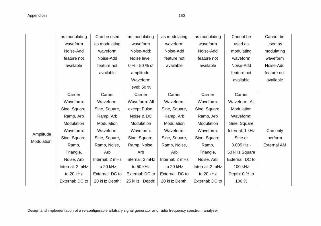
Appendices 180
Design and implementation of a re-configurable arbitrary signal generator and radio frequency spectrum analyser
as modulating
waveform
Noise-Add
feature not
available
Can be used
as modulating
waveform
Noise-Add
feature not
available
as modulating
waveform
Noise-Add:
Noise level:
0 % - 50 % of
amplitude.
Waveform
level: 50 %
as modulating
waveform
Noise-Add
feature not
available
as modulating
waveform
Noise-Add
feature not
available
Cannot be
used as
modulating
waveform
Noise-Add
feature not
available
Cannot be
used as
modulating
waveform
Noise-Add
feature not
available
Amplitude
Modulation
Carrier
Waveform:
Sine, Square,
Ramp, Arb
Modulation
Waveform:
Sine, Square,
Ramp,
Triangle,
Noise, Arb
Internal: 2 mHz
to 20 kHz
External: DC to
Carrier
Waveform:
Sine, Square,
Ramp, Arb
Modulation
Waveform:
Sine, Square,
Ramp, Noise,
Arb
Internal: 2 mHz
to 20 kHz
External: DC to
20 kHz Depth:
Carrier
Waveform: All
except Pulse,
Noise & DC
Modulation
Waveform:
Sine, Square,
Ramp, Noise,
Arb
Internal: 2 mHz
to 50 kHz
External: DC to
25 kHz Depth:
Carrier
Waveform:
Sine, Square,
Ramp, Arb
Modulation
Waveform:
Sine, Square,
Ramp, Noise,
Arb
Internal: 2 mHz
to 20 kHz
External: DC to
20 kHz Depth:
Carrier
Waveform:
Sine, Square,
Ramp, Arb
Modulation
Waveform:
Sine, Square,
Ramp,
Triangle,
Noise, Arb
Internal: 2 mHz
to 20 kHz
External: DC to
Carrier
Waveform: All
Modulation
Waveform:
Sine, Square
Internal: 1 kHz
Sine or
0.005 Hz -
50 kHz Square
External: DC to
100 kHz
Depth: 0 % to
100 %
Can only
perform
External AM
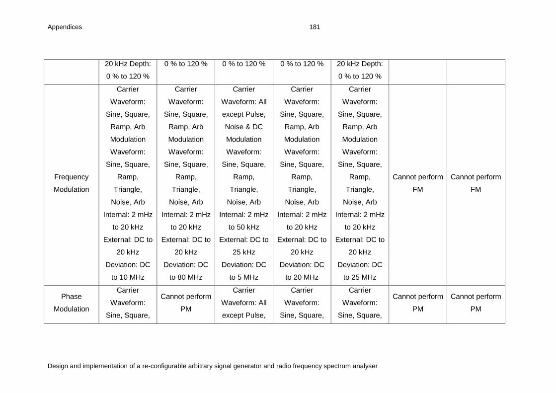
Appendices 181
Design and implementation of a re-configurable arbitrary signal generator and radio frequency spectrum analyser
20 kHz Depth:
0 % to 120 %
0 % to 120 % 0 % to 120 % 0 % to 120 % 20 kHz Depth:
0 % to 120 %
Frequency
Modulation
Carrier
Waveform:
Sine, Square,
Ramp, Arb
Modulation
Waveform:
Sine, Square,
Ramp,
Triangle,
Noise, Arb
Internal: 2 mHz
to 20 kHz
External: DC to
20 kHz
Deviation: DC
to 10 MHz
Carrier
Waveform:
Sine, Square,
Ramp, Arb
Modulation
Waveform:
Sine, Square,
Ramp,
Triangle,
Noise, Arb
Internal: 2 mHz
to 20 kHz
External: DC to
20 kHz
Deviation: DC
to 80 MHz
Carrier
Waveform: All
except Pulse,
Noise & DC
Modulation
Waveform:
Sine, Square,
Ramp,
Triangle,
Noise, Arb
Internal: 2 mHz
to 50 kHz
External: DC to
25 kHz
Deviation: DC
to 5 MHz
Carrier
Waveform:
Sine, Square,
Ramp, Arb
Modulation
Waveform:
Sine, Square,
Ramp,
Triangle,
Noise, Arb
Internal: 2 mHz
to 20 kHz
External: DC to
20 kHz
Deviation: DC
to 20 MHz
Carrier
Waveform:
Sine, Square,
Ramp, Arb
Modulation
Waveform:
Sine, Square,
Ramp,
Triangle,
Noise, Arb
Internal: 2 mHz
to 20 kHz
External: DC to
20 kHz
Deviation: DC
to 25 MHz
Cannot perform
FM
Cannot perform
FM
Phase
Modulation
Carrier
Waveform:
Sine, Square,
Cannot perform
PM
Carrier
Waveform: All
except Pulse,
Carrier
Waveform:
Sine, Square,
Carrier
Waveform:
Sine, Square,
Cannot perform
PM
Cannot perform
PM
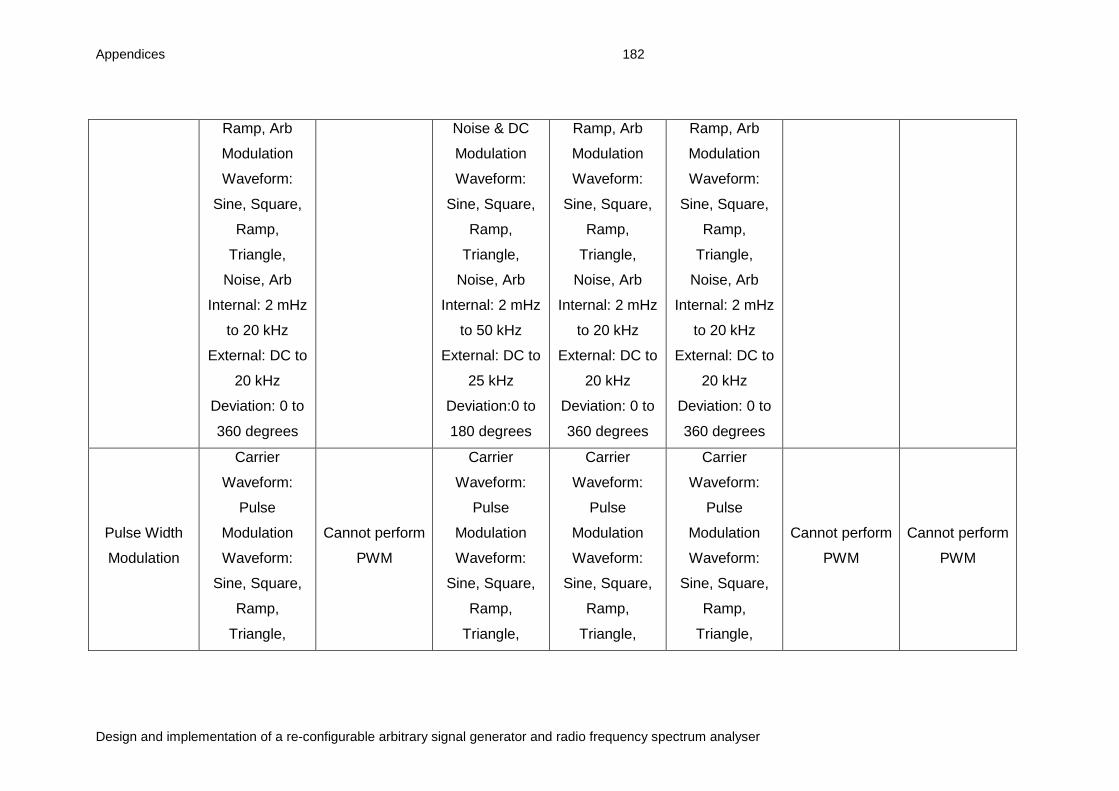
Appendices 182
Design and implementation of a re-configurable arbitrary signal generator and radio frequency spectrum analyser
Ramp, Arb
Modulation
Waveform:
Sine, Square,
Ramp,
Triangle,
Noise, Arb
Internal: 2 mHz
to 20 kHz
External: DC to
20 kHz
Deviation: 0 to
360 degrees
Noise & DC
Modulation
Waveform:
Sine, Square,
Ramp,
Triangle,
Noise, Arb
Internal: 2 mHz
to 50 kHz
External: DC to
25 kHz
Deviation:0 to
180 degrees
Ramp, Arb
Modulation
Waveform:
Sine, Square,
Ramp,
Triangle,
Noise, Arb
Internal: 2 mHz
to 20 kHz
External: DC to
20 kHz
Deviation: 0 to
360 degrees
Ramp, Arb
Modulation
Waveform:
Sine, Square,
Ramp,
Triangle,
Noise, Arb
Internal: 2 mHz
to 20 kHz
External: DC to
20 kHz
Deviation: 0 to
360 degrees
Pulse Width
Modulation
Carrier
Waveform:
Pulse
Modulation
Waveform:
Sine, Square,
Ramp,
Triangle,
Cannot perform
PWM
Carrier
Waveform:
Pulse
Modulation
Waveform:
Sine, Square,
Ramp,
Triangle,
Carrier
Waveform:
Pulse
Modulation
Waveform:
Sine, Square,
Ramp,
Triangle,
Carrier
Waveform:
Pulse
Modulation
Waveform:
Sine, Square,
Ramp,
Triangle,
Cannot perform
PWM
Cannot perform
PWM

Appendices 183
Design and implementation of a re-configurable arbitrary signal generator and radio frequency spectrum analyser
Noise, Arb
Internal: 2 mHz
to 20 kHz
External: DC to
20 kHz
Deviation: 0 to
100 %
Noise, Arb
Internal: 2 mHz
to 50 kHz
External: DC to
25 kHz
Deviation:0 to
50 %
Noise, Arb
Internal: 2 mHz
to 20 kHz
External: DC to
20 kHz
Deviation: 0 to
100 %
Noise, Arb
Internal: 2 mHz
to 20 kHz
External: DC to
20 kHz
Deviation: 0 to
100 %
Frequency
Shift Keying
Carrier
Waveform:
Sine, Square,
Ramp, Arb
Source:
Internal/Extern
al Internal
Modulation:
50 % duty
cycle Square
(2 mHz to
100 kHz)
Carrier
Waveform:
Sine, Square,
Ramp, Arb
Source:
Internal/Extern
al Internal
Modulation:
50 % duty
cycle Square
(2 mHz to
100 kHz)
Carrier
Waveform: All
except Pulse,
Noise & DC
Source:
Internal/Extern
al Internal
Modulation:
2 mHz to
1 MHz
Carrier
Waveform:
Sine, Square,
Ramp, Arb
Source:
Internal/Extern
al Internal
Modulation:
50 % duty
cycle Square
(2 mHz to
100 kHz)
Carrier
Waveform:
Sine, Square,
Ramp, Arb
Source:
Internal/Extern
al Internal
Modulation:
50 % duty
cycle Square
(2 mHz to
100 kHz)
Carrier
Waveform: All
Source:
Internal/Extern
al/Manual
Internal
Modulation:
DC - 50 kHz
Carrier
Waveform: All
except Pulse
and Pulse
Train Source:
Internal/Extern
al/Manual
Internal
Modulation:
DC - 50 kHz
Sweep Waveforms:
Sine, Square,
Waveforms:
Sine, Square,
Waveforms: All
except Pulse,
Waveforms:
Sine, Square,
Waveforms:
Sine, Square,
Waveforms: All
Type:
Waveforms: All
except Pulse

Appendices 184
Design and implementation of a re-configurable arbitrary signal generator and radio frequency spectrum analyser
Ramp, Arb
Type:
Linear/Logarith
mic Mode:
Continuous or
Externally/Man
ually Triggered
Direction:
Up/Down
Sweep Time:
1 ms – 500 s
Programmable
Marker
Ramp, Arb
Type:
Linear/Logarith
mic Mode:
Continuous or
Externally/Man
ually Triggered
Direction:
Up/Down
Sweep Time:
1 ms – 500 s
Programmable
Marker
Noise & DC
Type:
Linear/Logarith
mic Mode:
Continuous or
Internally/Exter
nally Triggered
Direction:
Up/Down
Sweep Time:
1 ms – 300 s
Marker not
provided
Ramp, Arb
Type:
Linear/Logarith
mic Mode:
Continuous or
Externally/Man
ually Triggered
Direction:
Up/Down
Sweep Time:
1 ms – 500 s
Programmable
Marker
Ramp, Arb
Type:
Linear/Logarith
mic Mode:
Continuous or
Externally/Man
ually Triggered
Direction:
Up/Down
Sweep Time:
1 ms – 500 s
Programmable
Marker
Linear/Logarith
mic Mode:
Continuous or
Single or
Manually/Exter
nally Triggered
Direction:
Up/Down
Sweep Time:
10 ms – 999 s
Programmable
Marker
Type:
Linear/Logarith
mic Mode:
Continuous or
Single or
Manually/Exter
nally Triggered
Direction:
Up/Down/Up-
Down/Down-
Up
Sweep Time:
1 ms – 999 s
Programmable
Marker
Burst
Waveforms:
Sine, Square,
Ramp, Pulse,
Noise, Arb
Type: Counted
(1 to 50000
Waveforms:
Sine, Square,
Ramp, Pulse,
Noise, Arb
Type: Counted
(1 to 1000000
Waveforms: All
except Noise
and DC
Type: Counted
(1 to 1000000
cycles), Infinite,
Waveforms:
Sine, Square,
Ramp, Pulse,
Noise, Arb
Type: Counted
(1 to 50000
Waveforms:
Sine, Square,
Ramp, Pulse,
Noise, Arb
Type: Counted
(1 to 50000
Waveforms: All
standard and
arbitrary
Type: Counted
(1 to 1023
cycles), Gated
Waveforms: All
standard and
arbitrary
Type: Counted
(1 to 1048575
cycles), Gated
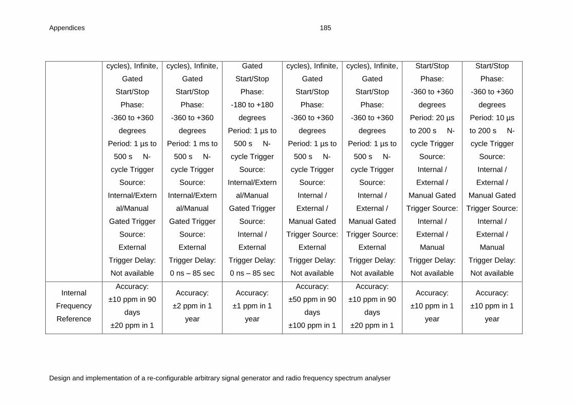
Appendices 185
Design and implementation of a re-configurable arbitrary signal generator and radio frequency spectrum analyser
cycles), Infinite,
Gated
Start/Stop
Phase:
-360 to +360
degrees
Period: 1 µs to
500 s N-
cycle Trigger
Source:
Internal/Extern
al/Manual
Gated Trigger
Source:
External
Trigger Delay:
Not available
cycles), Infinite,
Gated
Start/Stop
Phase:
-360 to +360
degrees
Period: 1 ms to
500 s N-
cycle Trigger
Source:
Internal/Extern
al/Manual
Gated Trigger
Source:
External
Trigger Delay:
0 ns – 85 sec
Gated
Start/Stop
Phase:
-180 to +180
degrees
Period: 1 µs to
500 s N-
cycle Trigger
Source:
Internal/Extern
al/Manual
Gated Trigger
Source:
Internal /
External
Trigger Delay:
0 ns – 85 sec
cycles), Infinite,
Gated
Start/Stop
Phase:
-360 to +360
degrees
Period: 1 µs to
500 s N-
cycle Trigger
Source:
Internal /
External /
Manual Gated
Trigger Source:
External
Trigger Delay:
Not available
cycles), Infinite,
Gated
Start/Stop
Phase:
-360 to +360
degrees
Period: 1 µs to
500 s N-
cycle Trigger
Source:
Internal /
External /
Manual Gated
Trigger Source:
External
Trigger Delay:
Not available
Start/Stop
Phase:
-360 to +360
degrees
Period: 20 µs
to 200 s N-
cycle Trigger
Source:
Internal /
External /
Manual Gated
Trigger Source:
Internal /
External /
Manual
Trigger Delay:
Not available
Start/Stop
Phase:
-360 to +360
degrees
Period: 10 µs
to 200 s N-
cycle Trigger
Source:
Internal /
External /
Manual Gated
Trigger Source:
Internal /
External /
Manual
Trigger Delay:
Not available
Internal
Frequency
Reference
Accuracy:
±10 ppm in 90
days
±20 ppm in 1
Accuracy:
±2 ppm in 1
year
Accuracy:
±1 ppm in 1
year
Accuracy:
±50 ppm in 90
days
±100 ppm in 1
Accuracy:
±10 ppm in 90
days
±20 ppm in 1
Accuracy:
±10 ppm in 1
year
Accuracy:
±10 ppm in 1
year
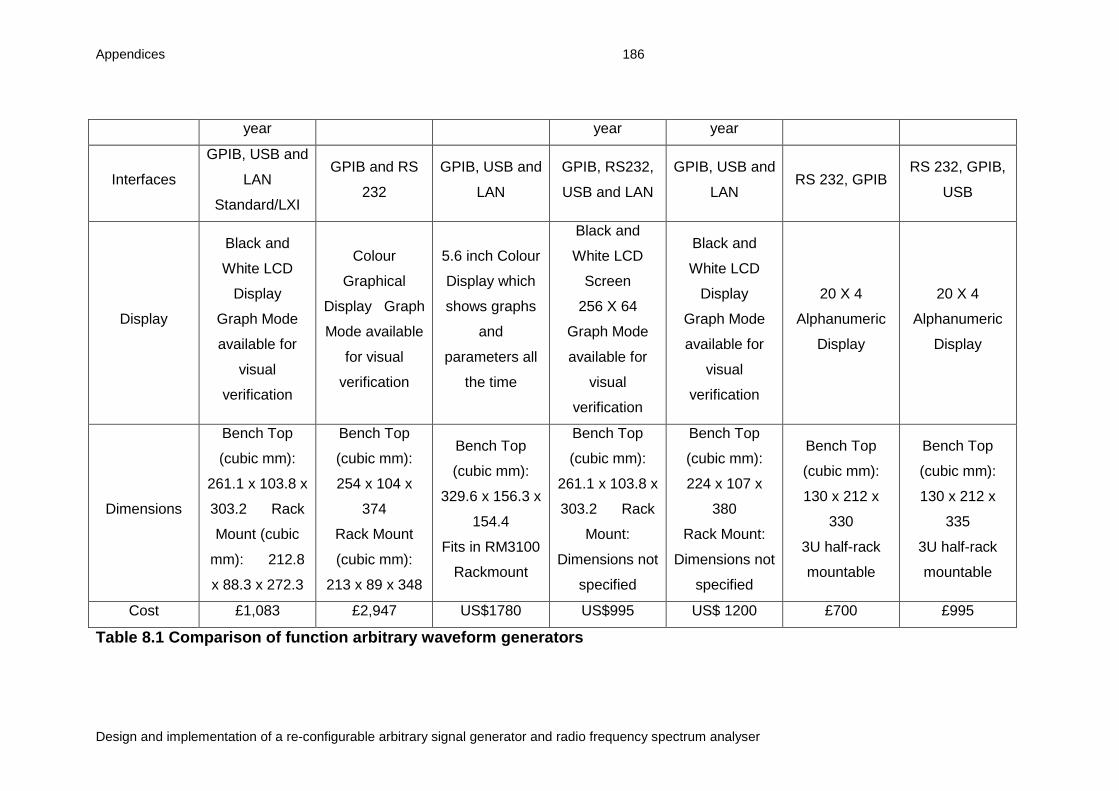
Appendices 186
Design and implementation of a re-configurable arbitrary signal generator and radio frequency spectrum analyser
year year year
Interfaces
GPIB, USB and
LAN
Standard/LXI
GPIB and RS
232
GPIB, USB and
LAN
GPIB, RS232,
USB and LAN
GPIB, USB and
LAN RS 232, GPIB
RS 232, GPIB,
USB
Display
Black and
White LCD
Display
Graph Mode
available for
visual
verification
Colour
Graphical
Display Graph
Mode available
for visual
verification
5.6 inch Colour
Display which
shows graphs
and
parameters all
the time
Black and
White LCD
Screen
256 X 64
Graph Mode
available for
visual
verification
Black and
White LCD
Display
Graph Mode
available for
visual
verification
20 X 4
Alphanumeric
Display
20 X 4
Alphanumeric
Display
Dimensions
Bench Top
(cubic mm):
261.1 x 103.8 x
303.2 Rack
Mount (cubic
mm): 212.8
x 88.3 x 272.3
Bench Top
(cubic mm):
254 x 104 x
374
Rack Mount
(cubic mm):
213 x 89 x 348
Bench Top
(cubic mm):
329.6 x 156.3 x
154.4
Fits in RM3100
Rackmount
Bench Top
(cubic mm):
261.1 x 103.8 x
303.2 Rack
Mount:
Dimensions not
specified
Bench Top
(cubic mm):
224 x 107 x
380
Rack Mount:
Dimensions not
specified
Bench Top
(cubic mm):
130 x 212 x
330
3U half-rack
mountable
Bench Top
(cubic mm):
130 x 212 x
335
3U half-rack
mountable
Cost £1,083 £2,947 US$1780 US$995 US$ 1200 £700 £995
Table 8.1 Comparison of function arbitrary waveform generators

Appendices 187
Design and implementation of a re-configurable arbitrary signal generator and radio frequency spectrum analyser
Appendix B: Target specification of the waveform generator
Issue 8: 27 October 2009
Specifications apply at 18 28 ºC after 30 minutes warmup, at maximum output into 50 Ω
Waveforms
Standard Waveforms
Sine, Square, Ramp (Variable Symmetry), Triangle, Negative Ramp, Pulse, Noise (Gaussian), DC,
Sin(x)/x, Exponential Rise, Exponential Fall, Logarithmic Rise, Logarithmic Fall and 4 User Defined
Arbitrary Waveforms.
Sine
Frequency Range: 1 µHz to 50 MHz
Frequency Resolution: 1 µHz, 14 digits
Output Level: 10 mVp-p to 10 Vpp into 50 Ω
Amplitude Flatness:
(Relative to 1 kHz)
<100kHz 0.1 dB
<5MHz 0.15 dB
<20MHz 0.3 dB
<50MHz 0.5 dB
Harmonic Distortion: <1 Vp-p ≥ 1 Vp-p
DC to 20 kHz -70 dBc -70 dBc
20 kHz to 100 kHz -65 dBc -60 dBc
100 kHz to 1 MHz -50 dBc -45 dBc
1 MHz to 20 MHz -40 dBc -35 dBc
20 MHz to 50 MHz -35 dBc -30 dBc
NonHarmonic Spurii: <–60 dBc to 1 MHz, <–60 dBc + 6 dB/octave 1 MHz to 50 MHz
Phase Noise (10 kHz offset): -115 dBc/Hz, typical (TBA)
Square
Frequency Range: 1 µHz to 50 MHz
Frequency Resolution: 1 µHz, 14 digits
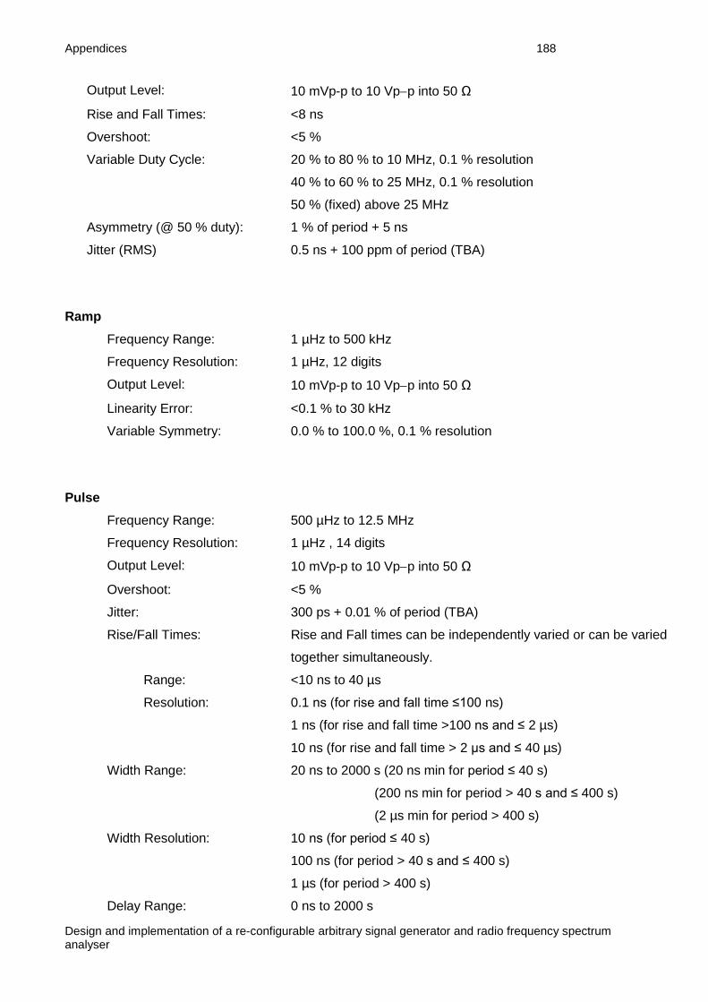
Appendices 188
Design and implementation of a re-configurable arbitrary signal generator and radio frequency spectrum analyser
Output Level: 10 mVp-p to 10 Vpp into 50 Ω
Rise and Fall Times: <8 ns
Overshoot: <5 %
Variable Duty Cycle: 20 % to 80 % to 10 MHz, 0.1 % resolution
40 % to 60 % to 25 MHz, 0.1 % resolution
50 % (fixed) above 25 MHz
Asymmetry (@ 50 % duty): 1 % of period + 5 ns
Jitter (RMS) 0.5 ns + 100 ppm of period (TBA)
Ramp
Frequency Range: 1 µHz to 500 kHz
Frequency Resolution: 1 µHz, 12 digits
Output Level: 10 mVp-p to 10 Vpp into 50 Ω
Linearity Error: <0.1 % to 30 kHz
Variable Symmetry: 0.0 % to 100.0 %, 0.1 % resolution
Pulse
Frequency Range: 500 µHz to 12.5 MHz
Frequency Resolution: 1 µHz , 14 digits
Output Level: 10 mVp-p to 10 Vpp into 50 Ω
Overshoot: <5 %
Jitter: 300 ps + 0.01 % of period (TBA)
Rise/Fall Times: Rise and Fall times can be independently varied or can be varied
together simultaneously.
Range: <10 ns to 40 µs
Resolution: 0.1 ns (for rise and fall time ≤100 ns)
1 ns (for rise and fall time >100 ns and ≤ 2 µs)
10 ns (for rise and fall time > 2 µs and ≤ 40 µs)
Width Range: 20 ns to 2000 s (20 ns min for period ≤ 40 s)
(200 ns min for period > 40 s and ≤ 400 s)
(2 µs min for period > 400 s)
Width Resolution: 10 ns (for period ≤ 40 s)
100 ns (for period > 40 s and ≤ 400 s)
1 µs (for period > 400 s)
Delay Range: 0 ns to 2000 s

Appendices 189
Design and implementation of a re-configurable arbitrary signal generator and radio frequency spectrum analyser
Delay Resolution: 10 ns (for period ≤ 40 s)
100 ns (for period > 40 s and ≤ 400 s)
1 µs (for period > 400 s)
Arbitrary
In built arbitrary waveforms (Sinc, Exponential Rise, Logarithmic Rise and DC). Up to 4 user defined
waveforms may be stored in non-volatile memory. Waveforms can be defined by downloading of
waveform data via remote interfaces or from the instrument’s front panel.
Waveform Memory Size: 4 waveforms – 4 waveforms of maximum size 65536 points or
3 waveforms – 1 waveform of maximum size 131072 points and 2
waveforms of maximum size 65536 points or
2 waveforms – 2 waveforms of maximum size 131072 points.
Minimum waveform size is 2 points.
Vertical Resolution: 14 bits
Frequency Range: 1 µHz to 10 MHz
Frequency Resolution: 1 µHz , 14 digits
Output Level: 10 mVp-p to 10V pp into 50 Ω
Sampling rate: 125 MS/s
Output Filter
Selects between 50 MHz Elliptic or 20 MHz Bessel filter depending on the waveform.
Noise
Gaussian White Noise: Noise can be added to any carrier waveform (except pulse and square and
noise itself). The amount of noise added can be specified as 0 % to 50 % of the amplitude of the
carrier waveform. Noise can also be used as modulating waveform.
Bandwidth (-3 dB): 20 MHz typical.
Noise crest factor (Vp/Vrms): 5.27
Output Level: 10 mVp-p to 10 Vpp into 50 Ω
Internal Frequency Reference
Oscillator Ageing Rate: 1 ppm first year
Temperature Stability: < 1 ppm over the specified temperature range

Appendices 190
Design and implementation of a re-configurable arbitrary signal generator and radio frequency spectrum analyser
Modulation
AM
Carrier Waveforms: Sine, Square, Ramp, Arb
Modulation Source: Internal/External
Internal Modulating
Waveforms:
Sine, Square, Up Ramp, Down Ramp, Triangle, Noise, DC, Sinc,
Exponential Rise, Logarithmic Rise and User Defined Arbs
Internal Modulating
Frequency:
1 µHz to 20 kHz, 1 µHz resolution
Amplitude Depth: 0.0 % to 120.0 %, 0.1 % resolution
FM
Carrier Waveforms: Sine, Square, Ramp, Arb
Modulation Source: Internal/External
Internal Modulating
Waveforms:
Sine, Square, Up Ramp, Down Ramp, Triangle, Noise, DC, Sinc,
Exponential Rise, Logarithmic Rise and User Defined Arbs
Internal Modulating
Frequency:
1 µHz to 20 kHz, 1 µHz resolution
Frequency Deviation: DC to Fmax/2, 1 µHz resolution
PM
Carrier Waveforms: Sine, Square, Ramp, Arb
Modulation Source: Internal/External
Internal Modulating
Waveforms:
Sine, Square, Up Ramp, Down Ramp, Triangle, Noise, DC, Sinc,
Exponential Rise, Logarithmic Rise and User Defined Arbs
Internal Modulating
Frequency:
1 µHz to 20 kHz, 1 µHz resolution
Phase Deviation: -360.0 to +360.0 degrees, 0.1 degree resolution
PWM
Carrier Waveforms: Pulse
Modulation Source: Internal/External
Internal Modulating
Waveforms:
Sine, Square, Up Ramp, Down Ramp, Triangle, Noise, DC, Sinc,
Exponential Rise, Logarithmic Rise and User Defined Arbs
Internal Modulating
Frequency:
1 µHz to 20 kHz, 1 µHz resolution
Pulse Width Deviation: 0 % to 100 % of pulse width, resolution same as of pulse width
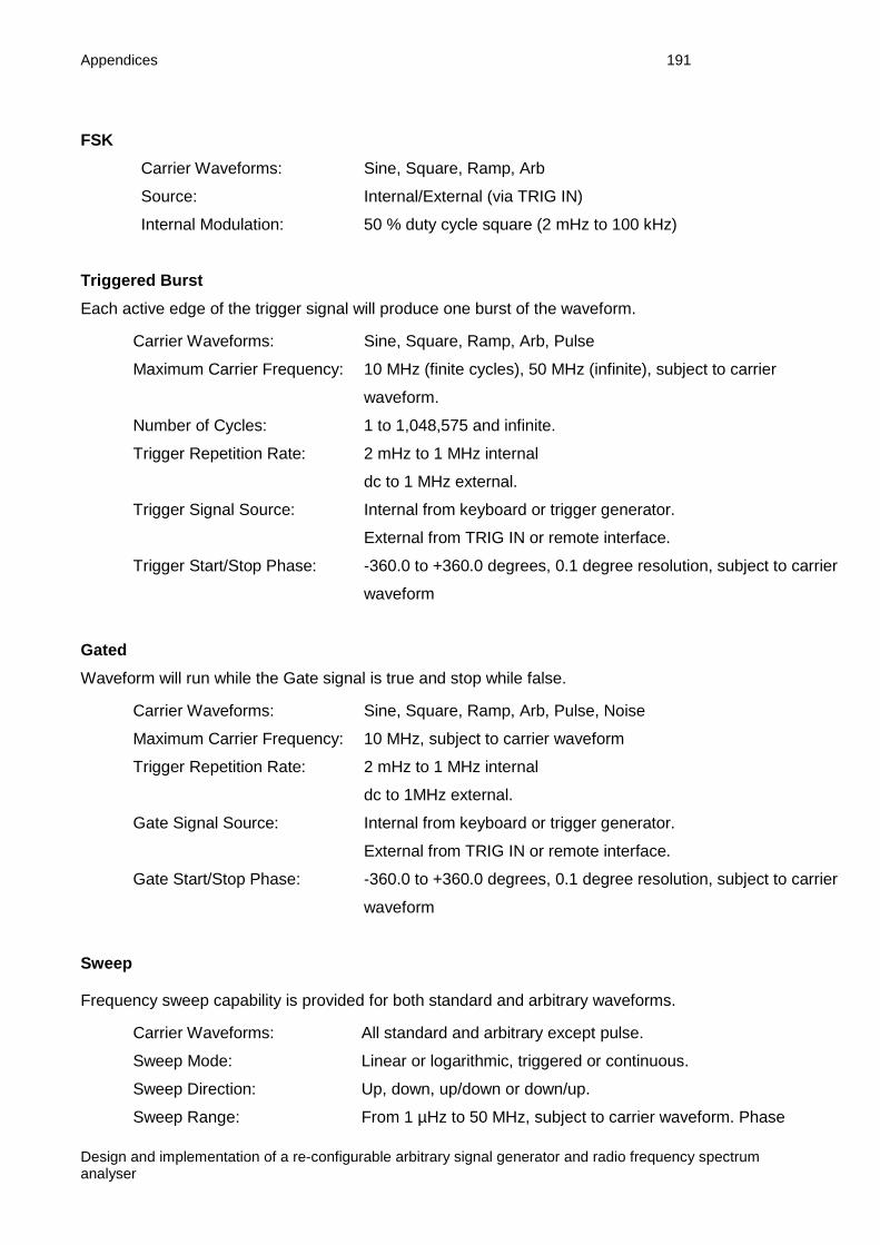
Appendices 191
Design and implementation of a re-configurable arbitrary signal generator and radio frequency spectrum analyser
FSK
Carrier Waveforms: Sine, Square, Ramp, Arb
Source: Internal/External (via TRIG IN)
Internal Modulation: 50 % duty cycle square (2 mHz to 100 kHz)
Triggered Burst
Each active edge of the trigger signal will produce one burst of the waveform.
Carrier Waveforms: Sine, Square, Ramp, Arb, Pulse
Maximum Carrier Frequency: 10 MHz (finite cycles), 50 MHz (infinite), subject to carrier
waveform.
Number of Cycles: 1 to 1,048,575 and infinite.
Trigger Repetition Rate: 2 mHz to 1 MHz internal
dc to 1 MHz external.
Trigger Signal Source: Internal from keyboard or trigger generator.
External from TRIG IN or remote interface.
Trigger Start/Stop Phase: -360.0 to +360.0 degrees, 0.1 degree resolution, subject to carrier
waveform
Gated
Waveform will run while the Gate signal is true and stop while false.
Carrier Waveforms: Sine, Square, Ramp, Arb, Pulse, Noise
Maximum Carrier Frequency: 10 MHz, subject to carrier waveform
Trigger Repetition Rate: 2 mHz to 1 MHz internal
dc to 1MHz external.
Gate Signal Source: Internal from keyboard or trigger generator.
External from TRIG IN or remote interface.
Gate Start/Stop Phase: -360.0 to +360.0 degrees, 0.1 degree resolution, subject to carrier
waveform
Sweep
Frequency sweep capability is provided for both standard and arbitrary waveforms.
Carrier Waveforms: All standard and arbitrary except pulse.
Sweep Mode: Linear or logarithmic, triggered or continuous.
Sweep Direction: Up, down, up/down or down/up.
Sweep Range: From 1 µHz to 50 MHz, subject to carrier waveform. Phase

Appendices 192
Design and implementation of a re-configurable arbitrary signal generator and radio frequency spectrum analyser
continuous. Independent setting of the start and stop frequency.
Sweep Time: 1 ms to 500 s (6 digit resolution).
Marker: Variable during sweep.
Sweep Trigger Source: The sweep may be free run or triggered from the following sources:
Internal from keyboard or trigger generator. Externally from TRIG IN
input or remote interface.
Trigger Generator
Internal source 2 mHz to 1 MHz square wave adjustable in 1 us steps, 9 digit resolution. Available for
external use from the SYNC OUT socket.
Outputs
Main Output
Output Impedance: 50 Ω
Amplitude: 20 mV to 20 Vpp open circuit (10 mV to 10 Vpp into 50 Ω). Amplitude
can be specified open circuit (hi Z) or into an assumed load of 1 Ω to
10 kΩ in Vpkpk, Vrms or dBm.
Amplitude Accuracy: 2 % ± 1 mV at 1 kHz into 50 Ω.
DC Offset Range: ±10 V. DC offset plus signal peak limited to ±10 V from 50 Ω.
DC Offset Accuracy: Typically 3 % ± 10 mV.
Resolution: 3 digits or 1 mV for both Amplitude and DC Offset.
Sync Out
Multifunction output user definable or automatically selected to be any of the following:
Carrier Waveform Sync:
Sine/Ramp/
Pulse
A square wave with 50 % duty cycle at the waveform
frequency.
Square A square wave with same duty cycle as the main output
at the waveform frequency.
Arbs A square wave with 50 % duty cycle at the waveform
frequency. The sync is a TTL high when the first point of
the waveform is output.
Noise No sync associated with noise.

Appendices 193
Design and implementation of a re-configurable arbitrary signal generator and radio frequency spectrum analyser
Modulation Sync: AM/FM/PM/
PWM
A square wave with 50 % duty cycle referenced to the
internal modulation waveform when modulation source is
internal, or a square wave referenced to the carrier
waveform when modulation source is external. No sync
is associated with noise as the modulation source.
FSK A square wave referenced to the trigger rate. The sync is
a TTL high when hop frequency is the output frequency
and TTL low when carrier frequency is the output
frequency for positive slope and vice versa for negative
slope.
Burst Sync: A square wave that is a TTL high when the burst begins and a TTL low
when burst is completed.
Trigger: Selects the current trigger signal. Useful for synchronizing burst or
gated signals.
Sweep Sync: Marker Off A square wave that is a TTL low from the midpoint of the
sweep and a TTL high from the end of the sweep.
Marker On A square wave that is a TTL low from the marker
frequency and a TTL high from the end of the sweep.
Output Signal Level: Logic level nominally 3 V.
Ref Clock Output
Buffered version of the 10 MHz clock currently in use (internal or external)
Output Level: Nominally 3 V logic level from 50 Ω
Inputs
Trig In
Frequency Range: DC 1 MHz.
Signal Range: Threshold nominally TTL level; maximum input ±10 V.
Minimum Pulse Width: 50 ns
Polarity: Selectable as high/rising edge or low/falling edge.
Input Impedance: 10 kΩ
External Modulation Input (for AM, FM, PM, PWM)
Voltage Range: ± 5 V full scale
Input Impedance: 5 kΩ typical
Bandwidh: DC to 20 kHz

Appendices 194
Design and implementation of a re-configurable arbitrary signal generator and radio frequency spectrum analyser
Ref Clock Input
Input for an external 10 MHz reference clock
Voltage Range: 1 Vpp – 5 Vpp
Maximum Voltage: +5 V
Minimum Voltage: -1 V
Phase synchronising two generators
Two generators can be synchronised together to provide outputs at the same frequency (or
harmonics) and with a phase difference. The amplitude and phase of these outputs can also be
modulated providing the capability to perform QAM and QPSK respectively. It is also possible to
synchronise more than two generators but results are not guaranteed.
Carrier Waveforms: Sine, Square, Ramp, Arb
Phase: Range -360.0 to +360.0 degrees
Resolution 0.1 degree
Accuracy < ±5 ns
Interfaces
Full digital remote control facilities are available through LAN and USB interfaces.
LAN Interface Ethernet 100/10 base – T hardware connection.
LXI V1.2, Class C compliant.
USB Interface Standard USB 2.0 hardware connection. Implemented as virtual-COM
port.
USB Flash Drive For waveform and setup storage/recall.
General
Display: Type: Monochrome Graphics Display
Pixel format: 112 COM X 256 SEG Matrix
Data Entry: Keyboard selection of mode, waveform etc.; value entry direct by
numeric keys or by rotary control.
Stored Settings:
(TBA)
Up to 9 complete instrument setups may be stored and recalled from
non-volatile memory.
Size: Bench Top: 97 mm height; 250 mm width; 270 mm long
Rack mount: 86.5 mm (2U) height; 213.5 mm (½rack) width; 244 mm
long
Weight: 2.55 kg
Power: 110-240 VAC ±10 % 50 / 60 Hz; 100 - 120 VAC ±10 % 400 Hz; 60 VA
max. Installation Category II.

Appendices 195
Design and implementation of a re-configurable arbitrary signal generator and radio frequency spectrum analyser
Operating Range: +5 °C to 40 °C, 20 80 % RH.
Storage Range: 20 °C to + 60 °C.
Environmental: Indoor use at altitudes up to 2000m, Pollution Degree 2.
Options: 19 inch rack mounting kit.
Safety: Complies with EN610101.
EMC: Complies with EN61326

Appendices 196
Design and implementation of a re-configurable arbitrary signal generator and radio frequency spectrum analyser
Appendix C: Comparison table of the digital spectrum analyser
The information provided here was true when the analysis was carried out. The specification of the spectrum analysers may have changed
since then.
Comparison Table (Version 14/07/2010)
Anritsu
MS2713E
[MS2721B]
Rohde &
Schwarz FSH6
Tektronix
SA2600
BK Precision
2658 [2658A]
(Micronix
MSA358
[MSA458] also
has the same
specification)
Willtek 9103 Spectran
HF6060V4
[HF6080V4]
Features /
Measurement
Capabilities
Occupied
bandwidth,
Channel
power, ACPR,
C/I,
Interference
analyser,
Spectrogram,
Signal
Spectrum
analysis, Scalar
network
analysis, Vector
network
analysis,
Receiver mode,
Channel power,
TDMA power,
Spectrum
management,
Spectrum
monitoring and
surveillance,
Interference
detection and
troubleshooting,
Signal hunting,
Channel power,
Adjacent
channel power,
Occupied
bandwidth,
Electric field
strength,
Magnetic field
strength,
Spectrum
analysis,
Channel power,
Adjacent
channel power,
Occupied
bandwidth, AM
and FM
demodulation,
Spectrum
analysis,
Analysis and
measurement of
WLAN, UMTS,
Wi-Fi, active
radar, GSM,
mobile phones,
blue-tooth,

Appendices 197
Design and implementation of a re-configurable arbitrary signal generator and radio frequency spectrum analyser
strength, RSSI,
Signal ID,
Gated sweep,
CW signal
generator,
Internal power
meter,
AM/FM/SSB
demodulation,
Emission
mask,
[Tracking
generator]
Occupied
bandwidth,
DTF, 3GPP
code domain
power, Isotropic
antenna, C/N
measurement,
Power,
Transducer
factors, Limit
lines, Display
line, AM and FM
audio
demodulation,
Tracking
generator
Signal
identification,
Signals
intelligence,
Homeland
security, AM
and FM
demodulation,
Signal strength
indicator,
Integrated GPS
receiver
Frequency
counter,
[Tracking
generator]
Signal
generator,
Transmission
measurement,
Reflection
measurement,
Distance to fault
measurement,
Cable loss
measurement,
EMC
measurement
microwave
ovens, DECT
phones,
TETRA, radio
stations and TV
stations, AM,
FM and PM
demodulation
Frequency
Range
100 kHz –
6 GHz [9 kHz -
7.1 GHz]
100 kHz –
6 GHz
10 kHz –
6.2 GHz
50 kHz -
8.5 GHz
100 kHz -
7.5 GHz
10 MHz –
6 GHz [10 MHz
– 8 GHz]
Maximum Span 6 GHz
[7.1 GHz]
6 GHz 6.2 GHz 8.5 GHz 7.5 GHz Not mentioned
(presumably

Appendices 198
Design and implementation of a re-configurable arbitrary signal generator and radio frequency spectrum analyser
5990 MHz
[7990 MHz])
Minimum Span 10 Hz including
zero span
100 Hz
including zero
span
10 kHz 200 kHz
including zero
span
10 kHz
including zero
span
Not mentioned
(zero span
available)
Frequency
Resolution
1 Hz 1 Hz 1 Hz 100 kHz
[20 kHz]
1 kHz Not mentioned
Frequency
Reference
Ageing:
±1.0 ppm /
10 years
Accuracy:
± 1.5 [0.3] ppm
(25 °C ± 25 °C)
+ ageing
Ageing:
1.0 ppm / year
Accuracy:
2 ppm (0 °C to
+30 °C)
+ 2 ppm / 10°C
(+30 °C to
+50 °C)
Ageing:
1.0 ppm / year
Accuracy:
0.5 ppm (0 °C to
+50 °C)
Ageing: -
Accuracy: -
Ageing:
± 1.5 ppm
Temperature
stability: ± 2ppm
Frequency
uncertainty: ±
1.5ppm
Ageing: -
Accuracy: -
Stability: -
Resolution
Bandwidth
10 Hz [1 Hz] –
3 MHz in 1 – 3
sequence
± 10 %, (1 MHz
max in zero
span) (-3 dB
100 Hz – 1 MHz
in 1 – 3
sequence (plus
200 kHz) ±5 %
(±10 % for
1 MHz) (-3 dB
10 Hz – 3 MHz
(manual), 10 Hz
– 1 MHz (auto),
Settable in 1 Hz
resolution
3 kHz – 3 MHz
in 1 – 3
sequence and
auto ± 20 %
(-3 dB
bandwidth)
100 Hz – 1 MHz
in 1 – 3
sequence,
manual or
automatic,
(-3dB
Minimum: 3 kHz
[1 kHz]
Maximum:
50 MHz
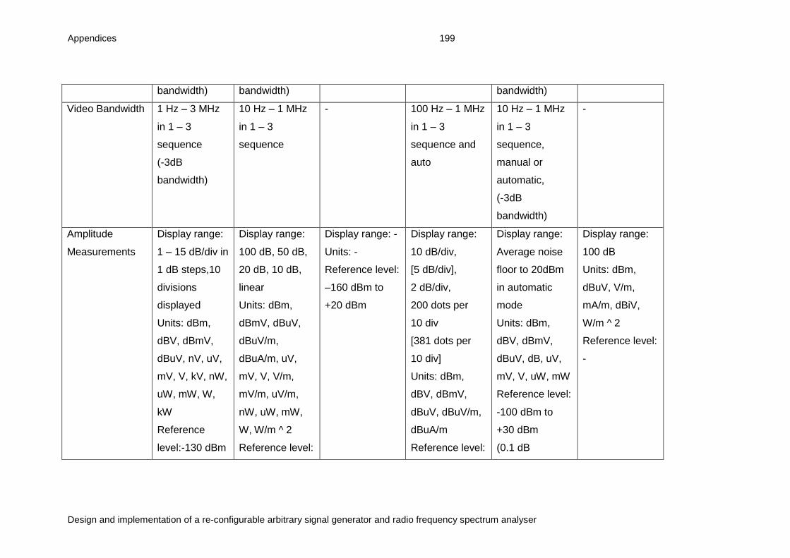
Appendices 199
Design and implementation of a re-configurable arbitrary signal generator and radio frequency spectrum analyser
bandwidth) bandwidth) bandwidth)
Video Bandwidth 1 Hz – 3 MHz
in 1 – 3
sequence
(-3dB
bandwidth)
10 Hz – 1 MHz
in 1 – 3
sequence
- 100 Hz – 1 MHz
in 1 – 3
sequence and
auto
10 Hz – 1 MHz
in 1 – 3
sequence,
manual or
automatic,
(-3dB
bandwidth)
-
Amplitude
Measurements
Display range:
1 – 15 dB/div in
1 dB steps,10
divisions
displayed
Units: dBm,
dBV, dBmV,
dBuV, nV, uV,
mV, V, kV, nW,
uW, mW, W,
kW
Reference
level:-130 dBm
Display range:
100 dB, 50 dB,
20 dB, 10 dB,
linear
Units: dBm,
dBmV, dBuV,
dBuV/m,
dBuA/m, uV,
mV, V, V/m,
mV/m, uV/m,
nW, uW, mW,
W, W/m ^ 2
Reference level:
Display range: -
Units: -
Reference level:
–160 dBm to
+20 dBm
Display range:
10 dB/div,
[5 dB/div],
2 dB/div,
200 dots per
10 div
[381 dots per
10 div]
Units: dBm,
dBV, dBmV,
dBuV, dBuV/m,
dBuA/m
Reference level:
Display range:
Average noise
floor to 20dBm
in automatic
mode
Units: dBm,
dBV, dBmV,
dBuV, dB, uV,
mV, V, uW, mW
Reference level:
-100 dBm to
+30 dBm
(0.1 dB
Display range:
100 dB
Units: dBm,
dBuV, V/m,
mA/m, dBiV,
W/m ^ 2
Reference level:
-
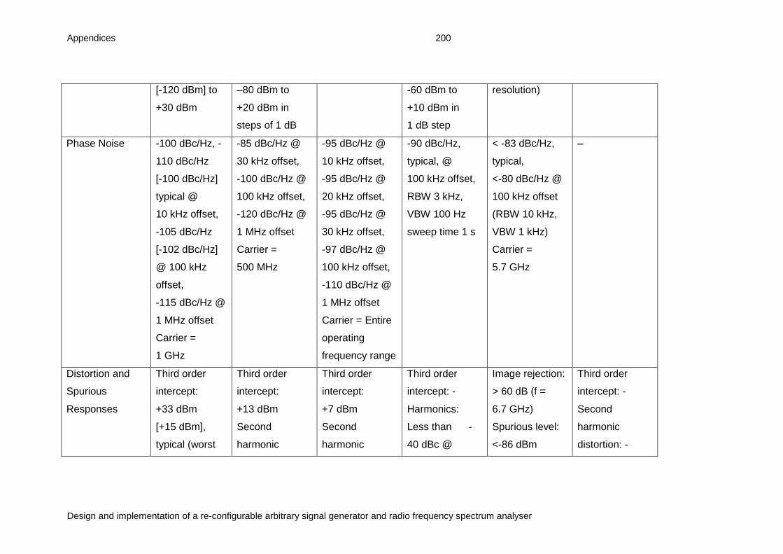
Appendices 200
Design and implementation of a re-configurable arbitrary signal generator and radio frequency spectrum analyser
[-120 dBm] to
+30 dBm
–80 dBm to
+20 dBm in
steps of 1 dB
-60 dBm to
+10 dBm in
1 dB step
resolution)
Phase Noise -100 dBc/Hz, -
110 dBc/Hz
[-100 dBc/Hz]
typical @
10 kHz offset,
-105 dBc/Hz
[-102 dBc/Hz]
@ 100 kHz
offset,
-115 dBc/Hz @
1 MHz offset
Carrier =
1 GHz
-85 dBc/Hz @
30 kHz offset,
-100 dBc/Hz @
100 kHz offset,
-120 dBc/Hz @
1 MHz offset
Carrier =
500 MHz
-95 dBc/Hz @
10 kHz offset,
-95 dBc/Hz @
20 kHz offset,
-95 dBc/Hz @
30 kHz offset,
-97 dBc/Hz @
100 kHz offset,
-110 dBc/Hz @
1 MHz offset
Carrier = Entire
operating
frequency range
-90 dBc/Hz,
typical, @
100 kHz offset,
RBW 3 kHz,
VBW 100 Hz
sweep time 1 s
< -83 dBc/Hz,
typical,
<-80 dBc/Hz @
100 kHz offset
(RBW 10 kHz,
VBW 1 kHz)
Carrier =
5.7 GHz
–
Distortion and
Spurious
Responses
Third order
intercept:
+33 dBm
[+15 dBm],
typical (worst
Third order
intercept:
+13 dBm
Second
harmonic
Third order
intercept:
+7 dBm
Second
harmonic
Third order
intercept: -
Harmonics:
Less than -
40 dBc @
Image rejection:
> 60 dB (f =
6.7 GHz)
Spurious level:
<-86 dBm
Third order
intercept: -
Second
harmonic
distortion: -

Appendices 201
Design and implementation of a re-configurable arbitrary signal generator and radio frequency spectrum analyser
case)
Second
harmonic
distortion:
-80 dBc
[-70 dBc]
(worst case)
Residual
Spurious
Responses: -
90 dBm
[-84 dBm]
distortion:
-60 dBc
Residual
Spurious
Responses:
-80 dBc
distortion:
-60 dBc
Residual
Spurious
Responses:
-90 dBc
>= 100 MHz
Spurious
response: Less
than -60 dBc
(100 kHz to
3 GHz),
<-80 dBm
(3 GHz to
7.5 GHz, 0 dB
attenuation)
LO leakage:
<-57 dBm (f =
7.7 GHz, 10 dB
attenuation)
Residual
Spurious
Responses: -
Displayed
Average Noise
Floor
–131 dBm,
typical
(-20 dBm
reference level,
1 Hz RBW)
–135 dBm,
typical (-30 dBm
reference level,
100 Hz RBW)
–145 dBm
(5 GHz -
6.2 GHz, 10 Hz
RBW)
–117 dBm
[–127 dBm],
typical, @
1 GHz
10 MHz to
5 GHz
–123 dBm,
typical
5 GHz to
7.5 GHz:
-120 dBm,
typical
(0 dBm
–135 dBm
[–145 dBm]
(1 Hz RBW)

Appendices 202
Design and implementation of a re-configurable arbitrary signal generator and radio frequency spectrum analyser
reference level,
100 Hz RBW)
Sweep Functions Sweep: Single,
continuous,
manual trigger,
reset,
detection,
minimum
sweep time,
trigger type,
gated sweep
Detection:
Peak, RMS,
negative,
sample, quasi
peak
Triggers: Free
run, external,
video, change
position,
manual
Sweep: Single,
continuous,
triggered
Detection: Auto
peak, RMS,
sample,
max/min peak
Triggers: Free
run, external,
video
Sweep: Single,
continuous, IF
level, external,
internal trigger
Detection: -
Triggers: Free
run, internal,
external, IF
level
Sweep: Normal,
maximum hold,
minimum hold,
average,
overwrite,
number of
sweeps 2 to
1024 (power of
2) and infinite
Detection:
Positive peak,
negative peak,
sample
Triggers:
Internal,
[External]
Sweep: Actual,
average,
maximum hold,
minimum hold
Detection:
Positive peak,
negative peak,
sample, RMS
(optional)
Triggers: Free
run
Sweep:
Start/stop,
centre/span
Detection: -
Triggers: Free
run

Appendices 203
Design and implementation of a re-configurable arbitrary signal generator and radio frequency spectrum analyser
Sweep-Time 10 us to 600 s
in zero span,
100 ms
minimum in
non-zero span
[auto set in
non-zero span]
1 ms to 100 s in
zero span,
20 ms to 1000 s
in non-zero
span
- 10 ms to 30 s
(1 – 3 step,
span 0 to
2 GHz) and
AUTO,
30 ms to 30 s
(1 – 3 step span
5 GHz and full)
and AUTO
1 ms to 250 s in
zero span,
1 ms to 250 s
for span
>= 10 kHz
-
Marker / Limit
Line / Trace
Functions
Markers: 1 – 6,
delta markers,
marker table,
fixed/tracking
marker, noise
marker,
frequency
counter
marker, on/off
Limit line:
Upper/lower,
on/off, edit,
Markers: 1 – 6,
delta marker,
multi-marker,
peak, next
peak, centre
frequency
marker,
reference level
marker, normal,
noise marker,
frequency
counter marker,
Markers: -
Limit line: -
Trace: -
Markers:
Normal and
delta markers,
displays
frequency, level,
frequency
difference and
level difference
Limit line: -
Trace: -
Markers: 6
(maximum), 5
delta markers,
marker
functions
(maximum,
peak, next
peak), transfer
functions
(centre
frequency,
reference level,
Markers: 1,2, or
3, frequency
marker,
amplitude
marker
Limit line: -
Trace: -

Appendices 204
Design and implementation of a re-configurable arbitrary signal generator and radio frequency spectrum analyser
move,
envelope,
advanced, limit
alarm, default
limit
Trace: Up to 3,
view/blank,
write/hold,
trace A/B/C
operations
on/off
Limit line:
function
available
(details not
provided in the
specifications)
Trace: 1 trace
and 1 memory
trace, A-B, B-A
trace
frequency step)
Limit line:
Upper, lower,
upper and
lower, 99 limit
templates, 30
limit segments
Trace: Up to 2,
minimum hold,
maximum hold
at the same
time, trace
functions (A+B
to A, A-B to A),
trace offset,
copy A>B, copy
B>A
RF Input Type: Type N,
female 50 ohm,
Maximum
input:+30 dBm,
Type: Type N,
female 50 ohm,
Maximum input:
-
Type: Type N,
female 50 ohm,
Maximum input:
+20 dBm
Type: Standard
SMA connector
[Type N, female
50 ohm],
Type: Type N,
female 50 ohm,
Maximum input:
+30 dBm,
Type: Standard
SMA connector,
50 ohm
Maximum input:

Appendices 205
Design and implementation of a re-configurable arbitrary signal generator and radio frequency spectrum analyser
±50 VDC,
VSWR: 2:1
[2:1 max, 1.5:1]
typical
VSWR: 1.5:1,
nominal
VSWR: - Maximum input:
+27 dBm,
+25 VDC
VSWR: < 2.0
±50 VDC,
VSWR: < 1.6,
typical, <1.3
(100 MHz to
4 GHZ), < 2.0,
typical, <1.6
(4 GHz to
6 GHz), <2.3,
typical, < 2.0
(6 GHz to
7.5 GHz)
+10 dBm
VSWR: -
Connectors /
Interfaces
Connectors:
Power
connector,
headset jack,
GPS, RF out
[not present],
external
reference input
[not present],
external
Connectors:
Power
connector,
headset jack,
trigger/external
reference input,
tracking
generator
output
Interfaces: RS-
Connectors: IF
output, external
reference input,
integrated GPS
receiver, Power
connector,
headset jack
Interfaces: LAN
Connectors:
Power
connector,
[external trigger
input], [external
trigger output]
Interfaces:
RS232C [not
present], [Type
A USB
Connectors:
Multi port 7 pin
ODU, DC input,
headset jack,
external
reference input
Interfaces: LAN
(TCP/IP)
interface, serial
interface
Connectors:
Power
connector,
audio connector
Interfaces: Mini
B USB interface

Appendices 206
Design and implementation of a re-configurable arbitrary signal generator and radio frequency spectrum analyser
trigger/clock
recovery
[external
trigger in]
Interfaces:
Type A USB
interface, mini
B USB
interface, [type
I compact flash
interface], [LAN
connection]
232-C optical
interface, power
sensor
interface], [mini
B USB
interface]
Memory Internal
memory: 2000
[>13000] traces
and setups
External
memory: USB
flash drive
[USB flash
drive, compact
Internal
memory: 256
traces and
setups (CMOS
RAM)
External
memory: None
Save/Recall:
Setups,
Internal
memory: -
External
memory: -
Save/Recall: -
Internal
memory: 100
[200] setups
and spectrum
measurements
External
memory: None
Save/Recall:
Setups and
Type: Flash disk
Capacity: 257
setups and
traces
Save/Recall:
Setups and
measurements
Internal
memory: 64 K
internal memory
External
memory: None
Save/Recall:
Setups,
measurements

Appendices 207
Design and implementation of a re-configurable arbitrary signal generator and radio frequency spectrum analyser
flash module]
Save/Recall:
Setups,
measurements,
screen shots
(save only)
measurements,
screen shots
(save only)
measurements
Screen shots
can be directly
printed by
connecting a
printer
Display Type: Resistive
touch screen
daylight
viewable colour
LCD
Size: 8.4 ''
Resolution:
800 x 600
Type: Trans-
reflective LC
colour display
Size: 5.7 ''
Resolution: 320
x 240
Type: Trans-
reflective LCD
Size: 10.4 ''
(diagonal)
Resolution: 640
x 480 (VGA)
Type:
Monochrome
LCD, CFL
backlight [colour
TFT LCD, LED
backlight]
Size: 4.7 "
[5.7 '']
Resolution: 320
x 240 [640 x
480]
Type: TFT
colour (256
colours) 300 cd
brightness
Size: 6.5 "
Resolution: 640
x 480
Type: LC
display
Size: 14 "
Battery Type: Li-Ion
Operation:
3 hours
[2.5 hours],
Type: NiMH
Operation:
3 hours, typical
Power
Type: Li-Ion
Operation:
5 hours, typical
Type: NiMH [Li-
Ion]
Type: Li-Ion
Operation:
2 hours, typical
Type: Li-Po
power battery
Operation: -
Power

Appendices 208
Design and implementation of a re-configurable arbitrary signal generator and radio frequency spectrum analyser
typical Consumption:
7 W, typical
Consumption:
7.2 V,
1300 mAh
Dimensions 273 mm x
199 mm x
91 mm
[315 mm x
211 mm x
94 mm]
170 mm x
120 mm x
270 mm
255 mm x
330 mm x
125 mm
162 mm x
70 mm x
260 mm
[162 mm x
71 mm x
265 mm]
355 mm x
190 mm x
104 mm
260 mm x
86 mm x 23 mm
Weight 3.45 kg [3.1 kg] 2.5 kg 5.56 kg 1.7 kg [1.8 kg] 3.6 kg 0.420 kg
Cost $11950
[$13950]
$13465 £17,400 $10395
[$10995]
$19092, $14552
(refurbished)
€999.95 [€1298]
Table 8.2 Comparison of 6GHz hand-held radio frequency spectrum analysers
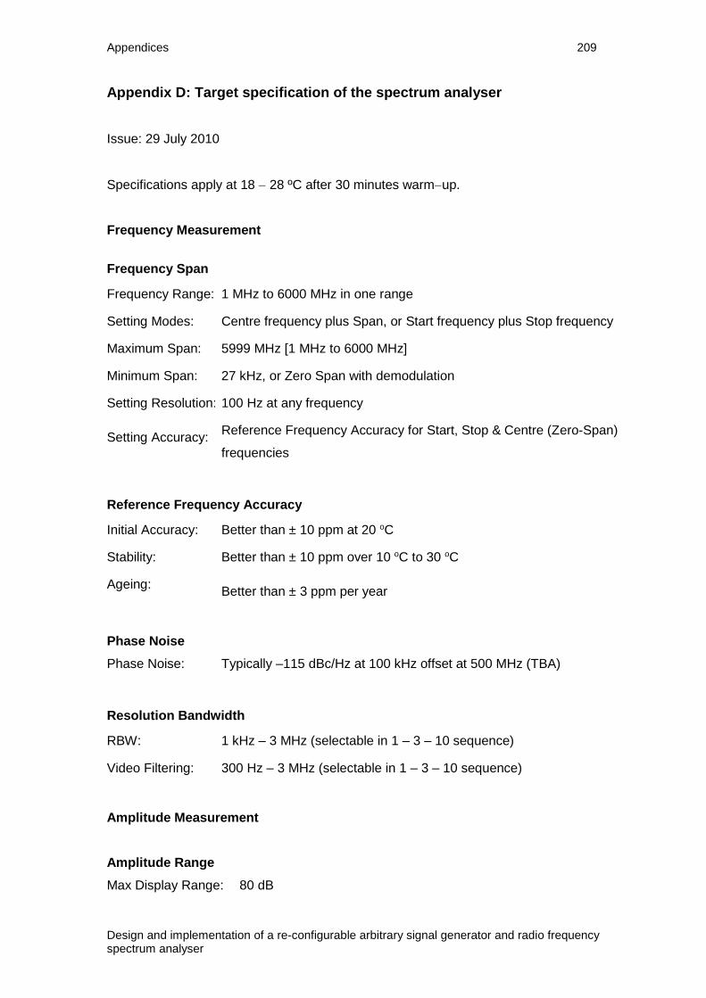
Appendices 209
Design and implementation of a re-configurable arbitrary signal generator and radio frequency spectrum analyser
Appendix D: Target specification of the spectrum analyser
Issue: 29 July 2010
Specifications apply at 18 28 ºC after 30 minutes warmup.
Frequency Measurement
Frequency Span
Frequency Range: 1 MHz to 6000 MHz in one range
Setting Modes: Centre frequency plus Span, or Start frequency plus Stop frequency
Maximum Span: 5999 MHz [1 MHz to 6000 MHz]
Minimum Span: 27 kHz, or Zero Span with demodulation
Setting Resolution: 100 Hz at any frequency
Setting Accuracy: Reference Frequency Accuracy for Start, Stop & Centre (Zero-Span)
frequencies
Reference Frequency Accuracy
Initial Accuracy: Better than ± 10 ppm at 20 oC
Stability: Better than ± 10 ppm over 10 oC to 30 oC
Ageing: Better than ± 3 ppm per year
Phase Noise
Phase Noise: Typically –115 dBc/Hz at 100 kHz offset at 500 MHz (TBA)
Resolution Bandwidth
RBW: 1 kHz – 3 MHz (selectable in 1 – 3 – 10 sequence)
Video Filtering: 300 Hz – 3 MHz (selectable in 1 – 3 – 10 sequence)
Amplitude Measurement
Amplitude Range
Max Display Range: 80 dB

Appendices 210
Design and implementation of a re-configurable arbitrary signal generator and radio frequency spectrum analyser
Measurement Units: DBm or dBµV (dB milli-watts or dB micro volts)
Reference Level: Selectable as –40 dBm, -20 dBm, 0 dBm or +20 dBm
Amplitude Accuracy
Ref. Level Accuracy: Better than ± 1 dB at 50 MHz at 10 dB below reference level (20 oC ± 5 oC)
Level Flatness: Better than ± 1.5 dB relative to 50 MHz over 1 MHz to 6000 MHz
Amplitude Linearity: Better than ± 1 dB over 50 dB range down from reference level
Amplitude Offset/Compensation
Offset: -40 dB to +40 dB, or None
Setting Resolution: 0.1 dB
User Defined Compensation: On, or Off. Enables or disables frequency dependent amplitude
to be compensated by adding a compensation value to the
displayed amplitude for the sweep.
Noise Floor
Noise Floor: Better than –110 dBm average displayed noise floor
(reference level = -40 dBm, RBW = 1 kHz)
Distortion and Spurious Responses
3rd Order Intermodulation: TBA
Harmonic: < –60 dBc at 10 dB below reference level (100 MHz)
1st Image: <– 50 dBc
Residual Spurious: <3 dB above noise floor
Markers
Number of Markers: One, Two (with Delta Marker), or None
Marker Resolution: Frequency 10 Hz at all frequencies
Amplitude 0.1 dB
Marker Accuracy: 1 / 270th of Frequency Span ± 10 Hz + Reference Frequency Accuracy
Frequency Readout: Frequency Display of absolute and difference frequencies for both markers

Appendices 211
Design and implementation of a re-configurable arbitrary signal generator and radio frequency spectrum analyser
Amplitude Display of absolute and difference amplitudes for both markers
Marker Functions: Normal, Peak Track, Frequency Counter
Limits
Limit Functions: High Line, Low Line, Scroll, User Defined Pattern, or Off
Line: Horizontal lines are created after comparing the amplitude of the active marker. Lines
can be moved up or down using the Scroll function.
Pattern: Pattern is created from a list of amplitude and frequency points. Straight lines
are drawn between these points.
Displayed Lines: One, two (or none) differentiated by colour.
Displayed Patterns: One, two (or none) differentiated by colour.
Storage: Any number of limit lines / patterns can be stored.
Traces
Live Trace: Dot-joined trace from current or held sweep. Selectable on or off.
Reference Trace: Stored trace either recalled from memory or copied directly from live trace.
Selectable on or off.
Trace Stores: Live only, Live + Ref, Ref Only, Store Live, Store Ref, Recall Ref.
Trace Mode: Normal, Average (Maximum 128), Peak Hold, Minimum Hold, Overwrite, Reset, Freeze,
Resume
Sweep
Sweep Method: Detection for 271 points per sweep. The amplitude value (as determined by the
detection method) from each sub-span is stored (sub-span = span / 270).
Sweep Time: Set automatically by Span and RBW.
Typically, 100 ms + 0.3 ms / MHz of span for RBW = 1 MHz
Sweep times will be higher for lower RBWs (TBA)
Fast (uncalibrated) sweep mode manually selectable.
Sweep Modes: Continuous – Free Run, Triggered Start, Triggered Stop, Gated Mode
Single – Free Run, Triggered Start

Appendices 212
Design and implementation of a re-configurable arbitrary signal generator and radio frequency spectrum analyser
Sweep Detection: Normal, Positive Peak, Negative Peak, Average
Sweep Control: Separate buttons for Run and Stop. Peak Hold and Average are reset
whenever Run is pressed.
Signal Input
Input Connector: Standard SMA /Type N connector (TBA), 50 Ω
VSWR: 1.5:1 typical
Absolute Maximum Input
Level:
+ 25 dBm or +132 dBµV (4 Vrms) or 15 V-DC
Demodulation (Zero Span mode)
Modes: AM or FM
Display: Swept trace with demodulation display. (TBA)
Audio Out: 30 mW into 32 Ω mono or stereo headphones, adjustable volume, 3.5 mm jack
socket (marked ) adjacent to the Signal Input.
Audio Filter Selectable low-pass filter to attenuate high frequency interference.
2 pole filter with turnover point at approximately 3 kHz.
Display
Display Type: Touchscreen Colour LCD
Trace Area: 271 x 225 pixels (high resolution mode).
Graticule: 8 x 10 divisions light grey graticule. Selectable as fully on, horizontal lines only,
or off.
Displayed Points: 271 points per sweep.
Resolution Modes: Selectable as High Resolution or Low Resolution *
*In low resolution mode the trace area becomes 135 x 112 points where each point is a block of
4 pixels. Only 135 sweep points are displayed. This mode is useful in situations where the
display could otherwise be difficult to see - e.g. when the instrument cannot be viewed at an
optimum distance.

Appendices 213
Design and implementation of a re-configurable arbitrary signal generator and radio frequency spectrum analyser
Memory Storage
Memory Type: Internal Non-volatile Flash memory, External USB
Flash Drive
Store Trace: Any number of traces can be stored under either default file
names or user entered file names. Traces are stored as
tables of amplitude versus frequency and can be imported
into other programs, as well as being recalled to the screen.
Recall Trace: Recalls any stored trace to the reference trace of the
display.
Store Set-up: Any number of instrument set-ups can be stored under
either default file names or user entered file names. All
settings of the instrument are saved.
Recall Set-up: Recalls any stored set-up, overwriting the existing settings
of the instrument.
Store Screen: This function copies the whole screen area to memory as a bit-
map. Any number of screens can be stored under either
default file names or user entered file names.
Store/Recall Limit Lines: Any number of limit lines can be stored under either default
file names or user entered file names, and recalled as
required.
Store/Recall Limit Patterns: Any number of limit patterns can be stored under either
default file names or user entered file names, and recalled
as required.
Store/Recall Compensation Files: Any number of compensation files can be stored under
either default file names or user entered file names, and
recalled as required.
Connectors
RF Input Connector: Standard SMA / Type N connector (TBA)
Power Connector: 1.3 mm (TBA) dc power socket (centre positive) for 5.2 V / 1 A (TBA)
external AC power adaptor/charger as supplied by TTi.
USB Connector: Type A USB connector to connect Flash Drive for store/recall functions
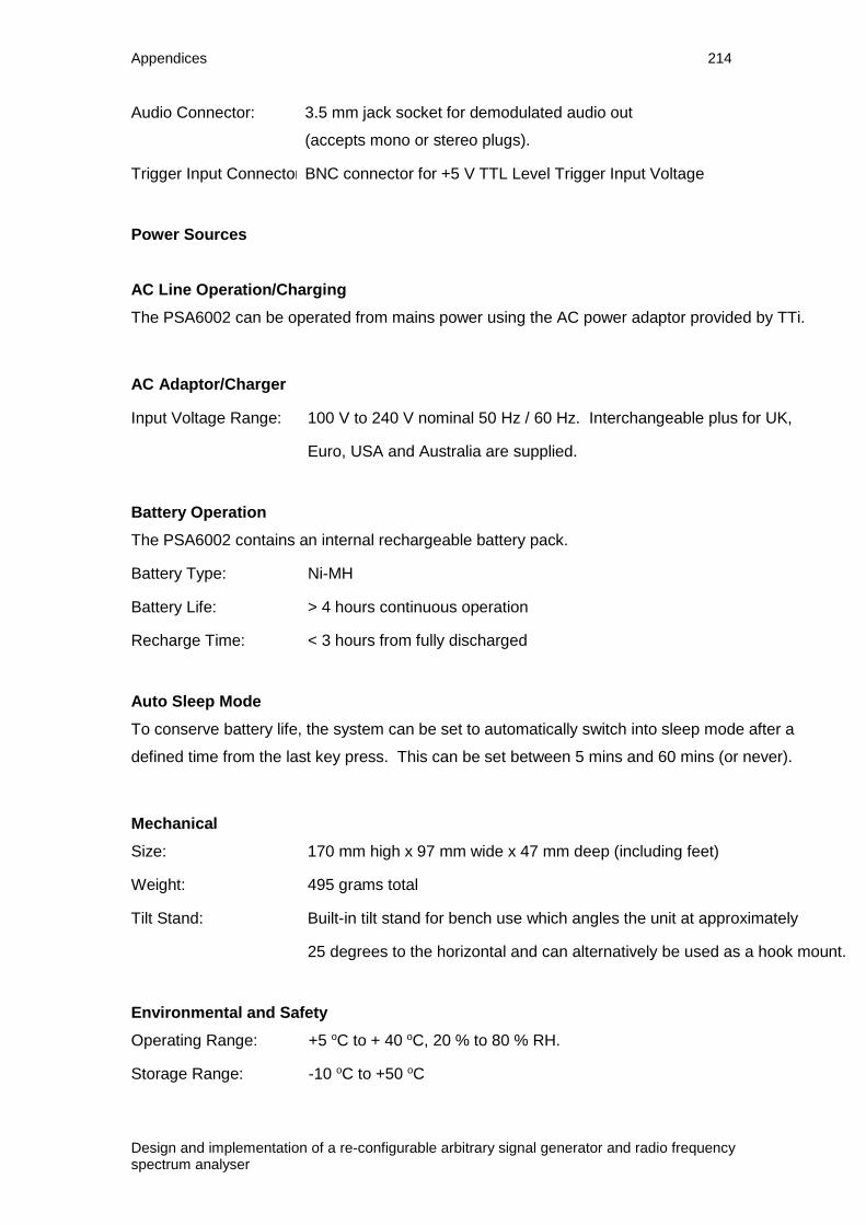
Appendices 214
Design and implementation of a re-configurable arbitrary signal generator and radio frequency spectrum analyser
Audio Connector: 3.5 mm jack socket for demodulated audio out
(accepts mono or stereo plugs).
Trigger Input Connector: BNC connector for +5 V TTL Level Trigger Input Voltage
Power Sources
AC Line Operation/Charging
The PSA6002 can be operated from mains power using the AC power adaptor provided by TTi.
AC Adaptor/Charger
Input Voltage Range: 100 V to 240 V nominal 50 Hz / 60 Hz. Interchangeable plus for UK,
Euro, USA and Australia are supplied.
Battery Operation
The PSA6002 contains an internal rechargeable battery pack.
Battery Type: Ni-MH
Battery Life: > 4 hours continuous operation
Recharge Time: < 3 hours from fully discharged
Auto Sleep Mode
To conserve battery life, the system can be set to automatically switch into sleep mode after a
defined time from the last key press. This can be set between 5 mins and 60 mins (or never).
Mechanical
Size: 170 mm high x 97 mm wide x 47 mm deep (including feet)
Weight: 495 grams total
Tilt Stand: Built-in tilt stand for bench use which angles the unit at approximately
25 degrees to the horizontal and can alternatively be used as a hook mount.
Environmental and Safety
Operating Range: +5 oC to + 40 oC, 20 % to 80 % RH.
Storage Range: -10 oC to +50 oC

Appendices 215
Design and implementation of a re-configurable arbitrary signal generator and radio frequency spectrum analyser
Environmental: Indoor use at altitudes to 2000 m, Pollution Degree 2.
Electrical Safety: Complies with EN61010-1.
EMC: Complies with EN61326.


![MPC8548E Configurable Development System … Configurable Development System Reference Manual, ... [4:0] ... MPC8548E Configurable Development System Reference Manual,](https://img.pdfslide.us/doc/110x75/5af028337f8b9ac62b8e4c0e/mpc8548e-configurable-development-system-configurable-development-system-reference.jpg)