Embed Size (px)
Citation preview
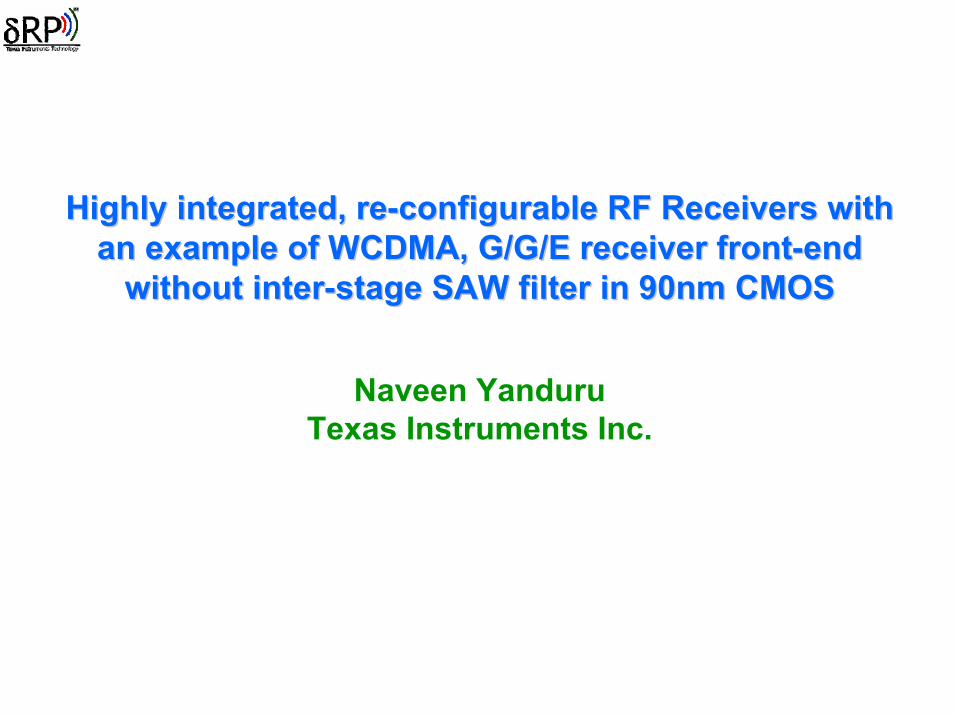
Highly integrated, reHighly integrated, re--configurable RF Receivers with configurable RF Receivers with an example of WCDMA, G/G/E receiver frontan example of WCDMA, G/G/E receiver front--end end
without interwithout inter--stage SAW filter in 90nm CMOSstage SAW filter in 90nm CMOS
Naveen YanduruTexas Instruments Inc.
1
Outline
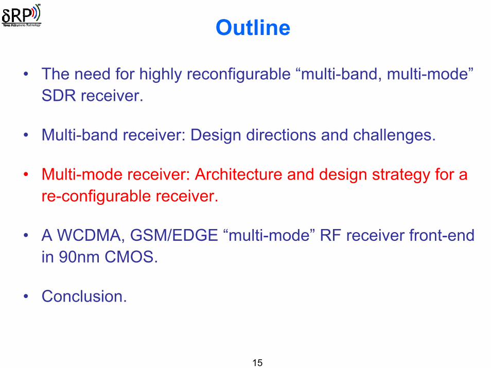
• The need for highly reconfigurable “multi-band, multi-mode”receiver.
• Multi-band receiver: Design directions and challenges.
• Multi-mode receiver: Architecture and design strategy for a re-configurable receiver.
• A WCDMA, GSM/EDGE “multi-mode” RF receiver front-end in 90nm CMOS.
• Conclusion.
2
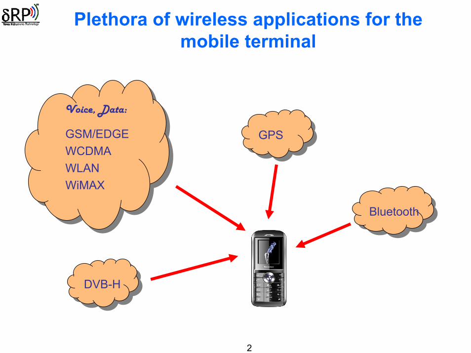
Plethora of wireless applications for the mobile terminal
GPS
Voice, Data:
GSM/EDGE WCDMA WLAN WiMAX
DVB-H
Bluetooth
3
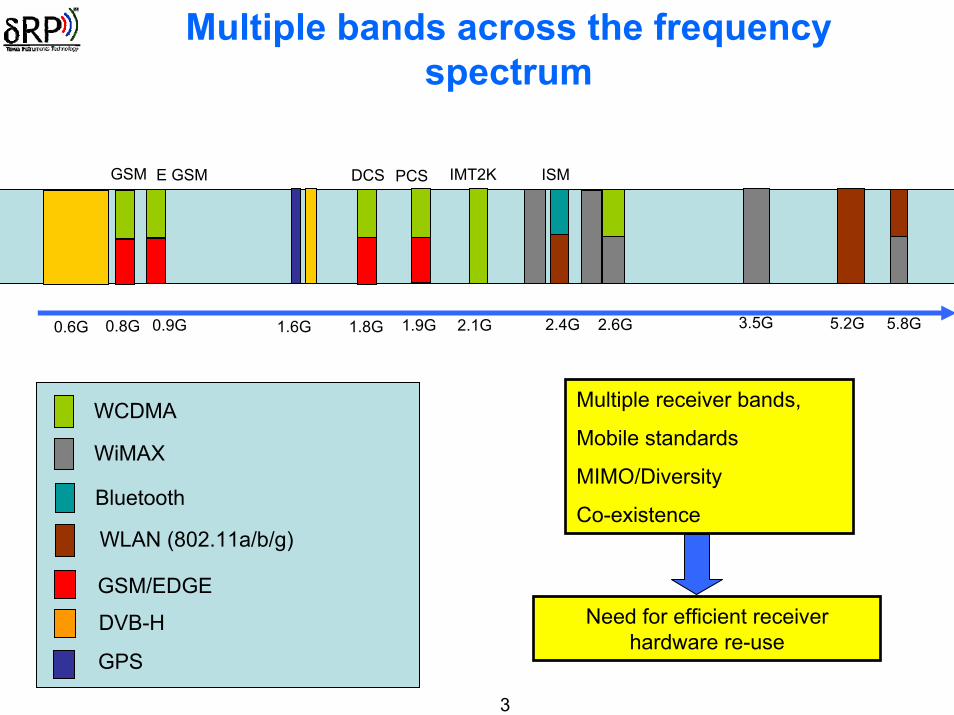
Multiple bands across the frequency spectrum
Multiple receiver bands,
Mobile standards
MIMO/Diversity
Co-existence
GSM E GSM PCS IMT2K ISM
0.8G 0.9G 1.6G 1.8G 1.9G 2.1G 2.4G 3.5G 5.2G2.6G0.6G
DCS
WCDMA
WLAN (802.11a/b/g)
WiMAX
DVB-H
GSM/EDGE
Bluetooth
GPS
Need for efficient receiver hardware re-use
5.8G
4
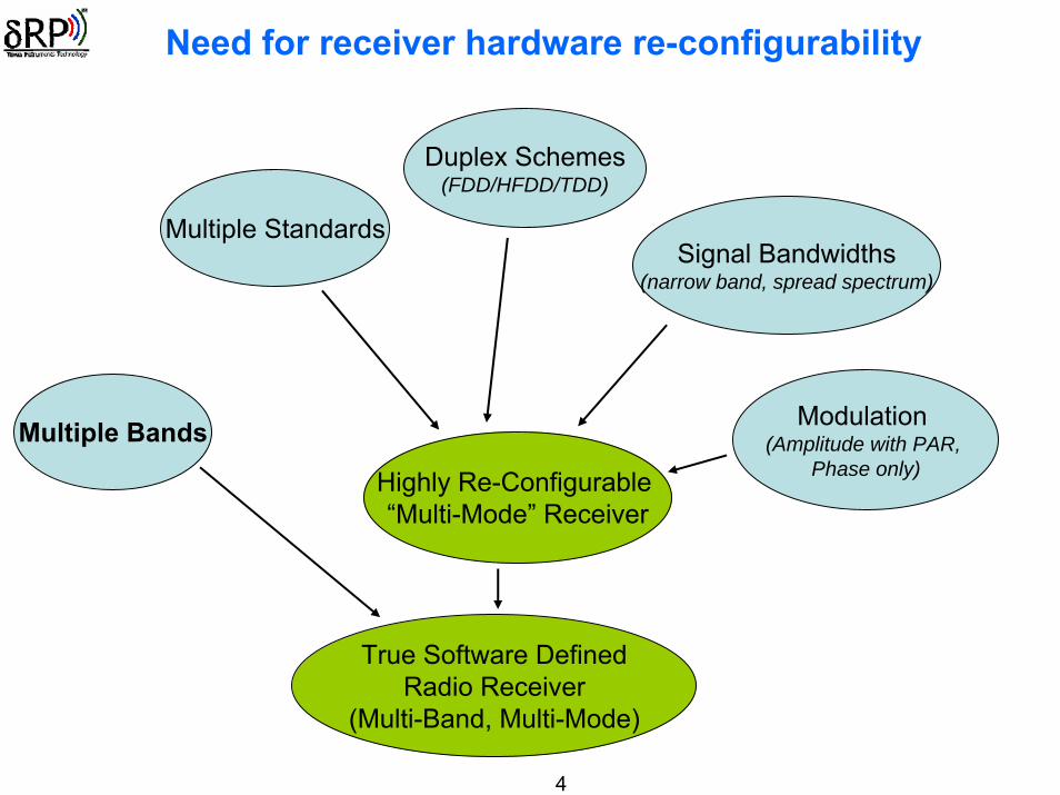
Need for receiver hardware re-configurability
Multiple Bands
Multiple Standards
Duplex Schemes(FDD/HFDD/TDD)
Modulation (Amplitude with PAR,
Phase only)
Signal Bandwidths(narrow band, spread spectrum)
Highly Re-Configurable “Multi-Mode” Receiver
True Software Defined Radio Receiver
(Multi-Band, Multi-Mode)
5
Outline
• The need for highly reconfigurable “multi-band, multi-mode”SDR receiver.
• Multi-band receiver: Design directions and challenges.
• Multi-mode receiver: Architecture and design strategy for a re-configurable receiver.
• A WCDMA, GSM/EDGE “multi-mode” RF receiver front-end in 90nm CMOS.
• Conclusion.
6
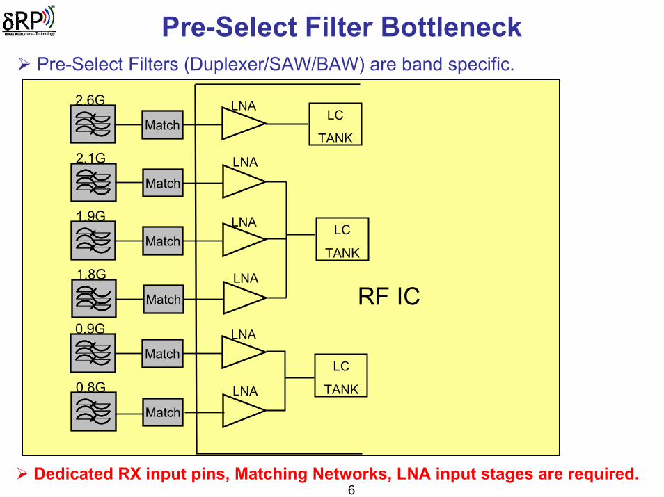
Pre-Select Filter Bottleneck
Dedicated RX input pins, Matching Networks, LNA input stages are required.
Pre-Select Filters (Duplexer/SAW/BAW) are band specific.
1.9G LNAMatch
RF IC1.8G LNA
Match
2.6G LNAMatch
2.1G LNAMatch
0.9G LNAMatch
0.8G LNAMatch
LC
TANK
LC
TANK
LC
TANK

Can we overcome this bottleneck?
8
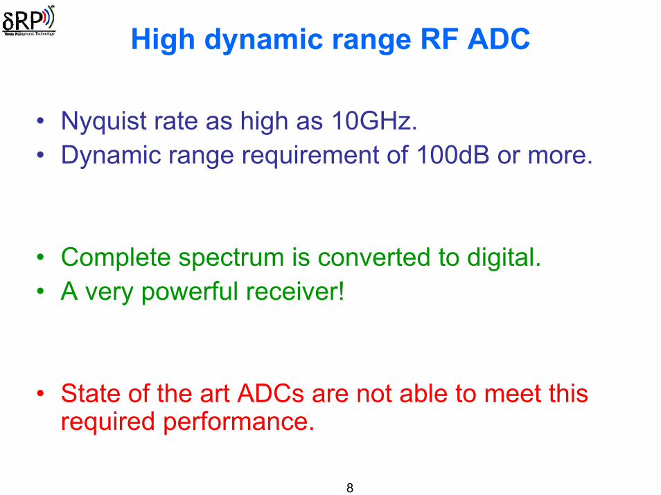
High dynamic range RF ADC
• Nyquist rate as high as 10GHz.• Dynamic range requirement of 100dB or more.
• Complete spectrum is converted to digital.• A very powerful receiver!
• State of the art ADCs are not able to meet this required performance.
9
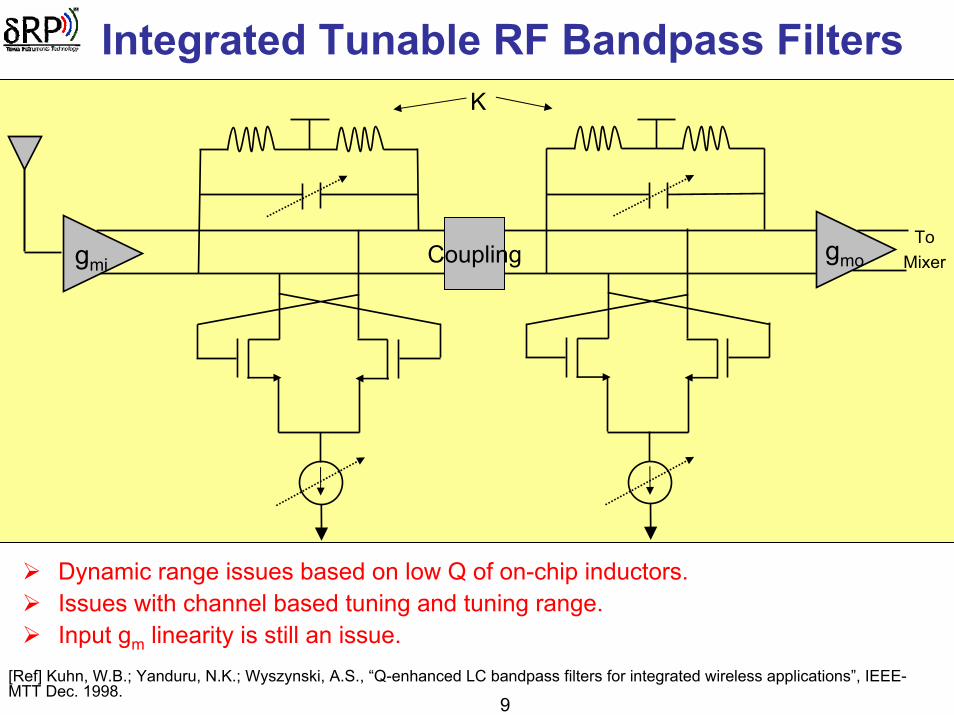
Integrated Tunable RF Bandpass Filters
Dynamic range issues based on low Q of on-chip inductors. Issues with channel based tuning and tuning range.Input gm linearity is still an issue.
gmi gmo
K
CouplingTo
Mixer
[Ref] Kuhn, W.B.; Yanduru, N.K.; Wyszynski, A.S., “Q-enhanced LC bandpass filters for integrated wireless applications”, IEEE-MTT Dec. 1998.
10
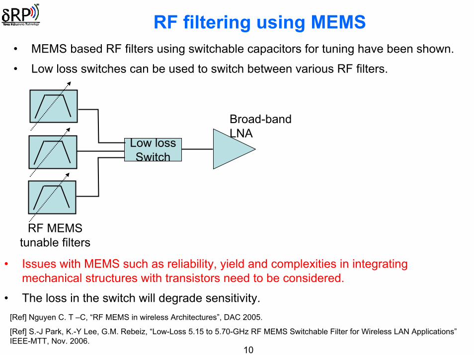
RF filtering using MEMS• MEMS based RF filters using switchable capacitors for tuning have been shown.
• Low loss switches can be used to switch between various RF filters.
• Issues with MEMS such as reliability, yield and complexities in integrating mechanical structures with transistors need to be considered.
• The loss in the switch will degrade sensitivity.
Low lossSwitch
Broad-band LNA
RF MEMS tunable filters
[Ref] Nguyen C. T –C, “RF MEMS in wireless Architectures”, DAC 2005.
[Ref] S.-J Park, K.-Y Lee, G.M. Rebeiz, “Low-Loss 5.15 to 5.70-GHz RF MEMS Switchable Filter for Wireless LAN Applications”IEEE-MTT, Nov. 2006.
11
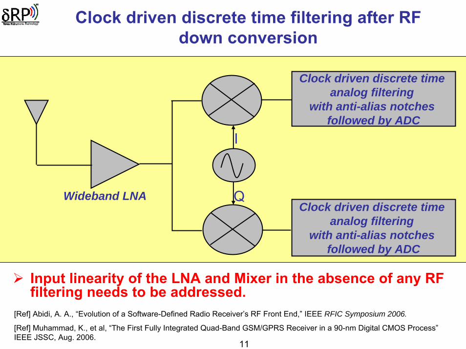
Clock driven discrete time filtering after RF down conversion
Input linearity of the LNA and Mixer in the absence of any RF filtering needs to be addressed.
Clock driven discrete time analog filtering
with anti-alias notches followed by ADC
Wideband LNA
I
QClock driven discrete time
analog filtering with anti-alias notches
followed by ADC
[Ref] Abidi, A. A., “Evolution of a Software-Defined Radio Receiver’s RF Front End,” IEEE RFIC Symposium 2006.
[Ref] Muhammad, K., et al, “The First Fully Integrated Quad-Band GSM/GPRS Receiver in a 90-nm Digital CMOS Process”IEEE JSSC, Aug. 2006.
12
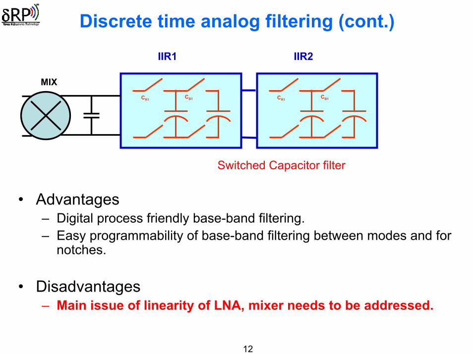
Discrete time analog filtering (cont.)
• Advantages– Digital process friendly base-band filtering.– Easy programmability of base-band filtering between modes and for
notches.
• Disadvantages– Main issue of linearity of LNA, mixer needs to be addressed.
Switched Capacitor filter
IIR1
CR1 CB1
IIR2
CR1 CB1
MIX
13
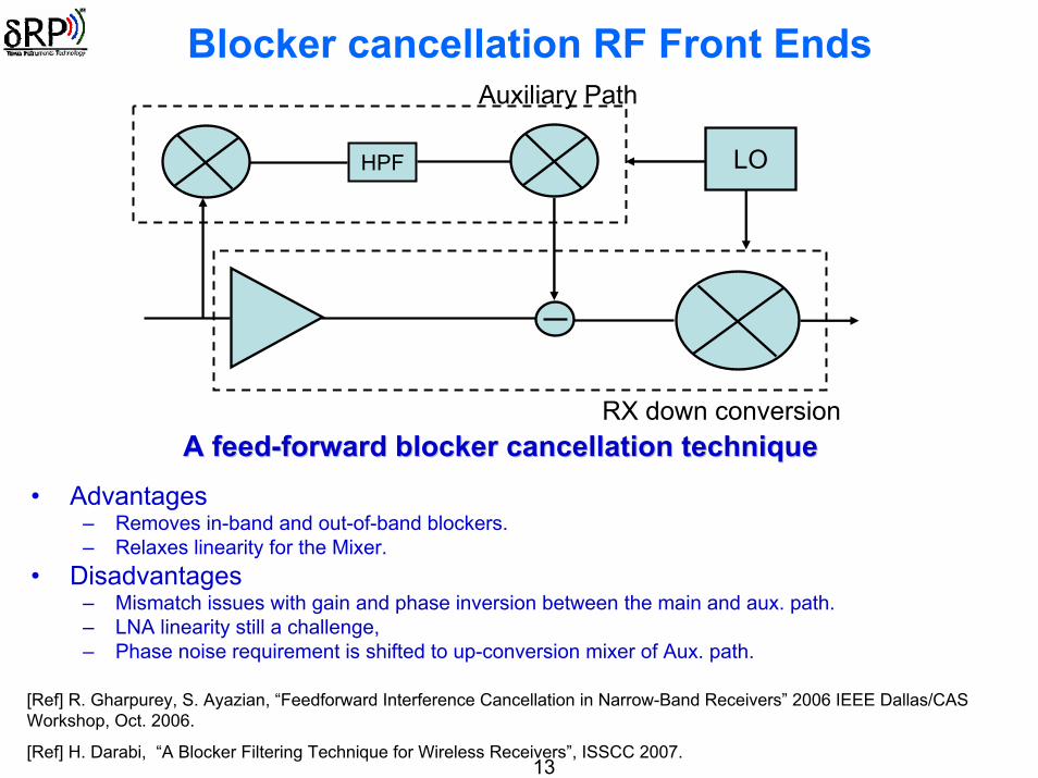
Blocker cancellation RF Front Ends
• Advantages– Removes in-band and out-of-band blockers.– Relaxes linearity for the Mixer.
• Disadvantages– Mismatch issues with gain and phase inversion between the main and aux. path.– LNA linearity still a challenge, – Phase noise requirement is shifted to up-conversion mixer of Aux. path.
LO
Auxiliary Path
RX down conversion
HPF
A feedA feed--forward blocker cancellation techniqueforward blocker cancellation technique
[Ref] R. Gharpurey, S. Ayazian, “Feedforward Interference Cancellation in Narrow-Band Receivers” 2006 IEEE Dallas/CAS Workshop, Oct. 2006.
[Ref] H. Darabi, “A Blocker Filtering Technique for Wireless Receivers”, ISSCC 2007.
Some other approaches including blocker detection using fast RSSI and subsequent reduction in RF gain have been investigated.
But these schemes along with other schemes discussed are not able to match the RF performance of a receiver with pre-select filter.
15
Outline
• The need for highly reconfigurable “multi-band, multi-mode”SDR receiver.
• Multi-band receiver: Design directions and challenges.
• Multi-mode receiver: Architecture and design strategy for a re-configurable receiver.
• A WCDMA, GSM/EDGE “multi-mode” RF receiver front-end in 90nm CMOS.
• Conclusion.
16
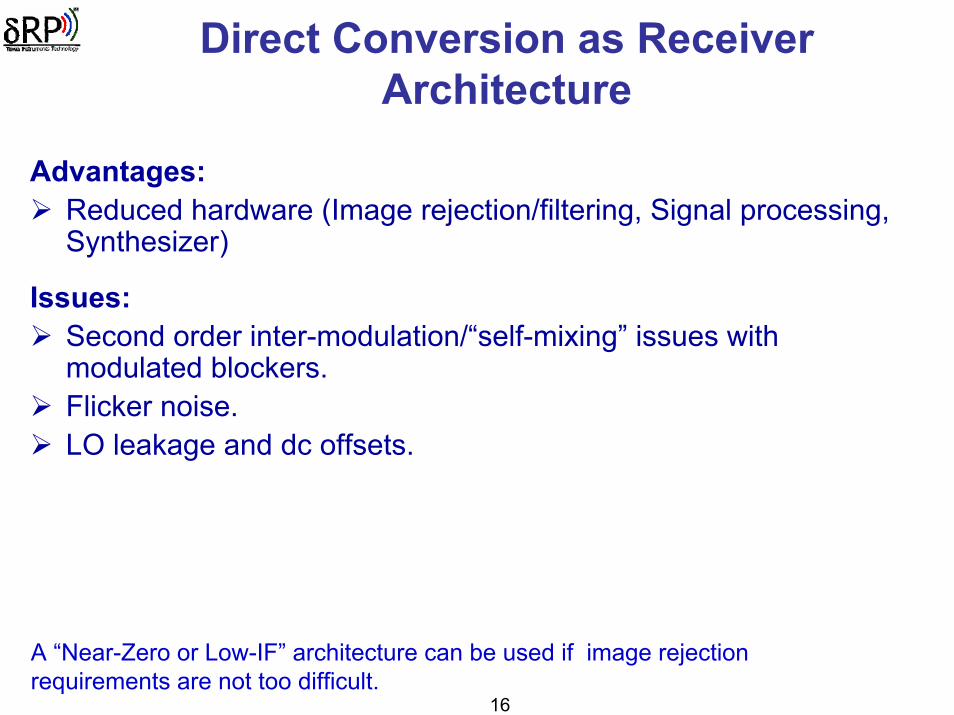
Direct Conversion as Receiver Architecture
Advantages:Reduced hardware (Image rejection/filtering, Signal processing, Synthesizer)
Issues:Second order inter-modulation/“self-mixing” issues with modulated blockers. Flicker noise.LO leakage and dc offsets.
A “Near-Zero or Low-IF” architecture can be used if image rejection requirements are not too difficult.
17
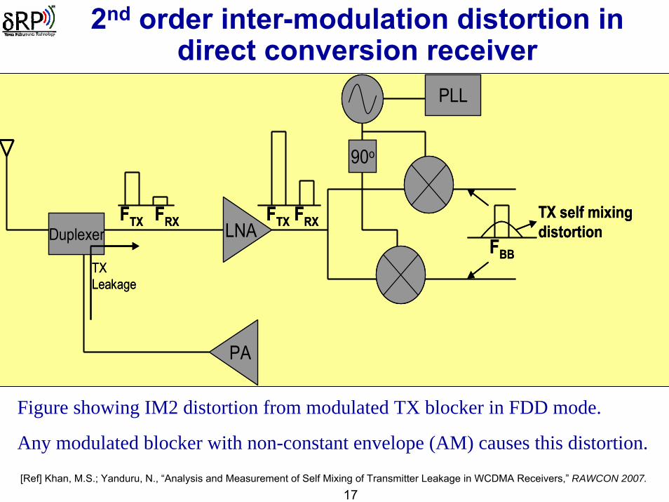
2nd order inter-modulation distortion in direct conversion receiver
LNADuplexer
PA
PLL
90o
TX Leakage
TX self mixing distortion
FTX FRX FRXFTX
FBB
LNADuplexer
PA
PLL
90o
TX Leakage
TX self mixing distortion
FTX FRX FRXFTX
FBB
Figure showing IM2 distortion from modulated TX blocker in FDD mode.
Any modulated blocker with non-constant envelope (AM) causes this distortion.
[Ref] Khan, M.S.; Yanduru, N., “Analysis and Measurement of Self Mixing of Transmitter Leakage in WCDMA Receivers,” RAWCON 2007.
18
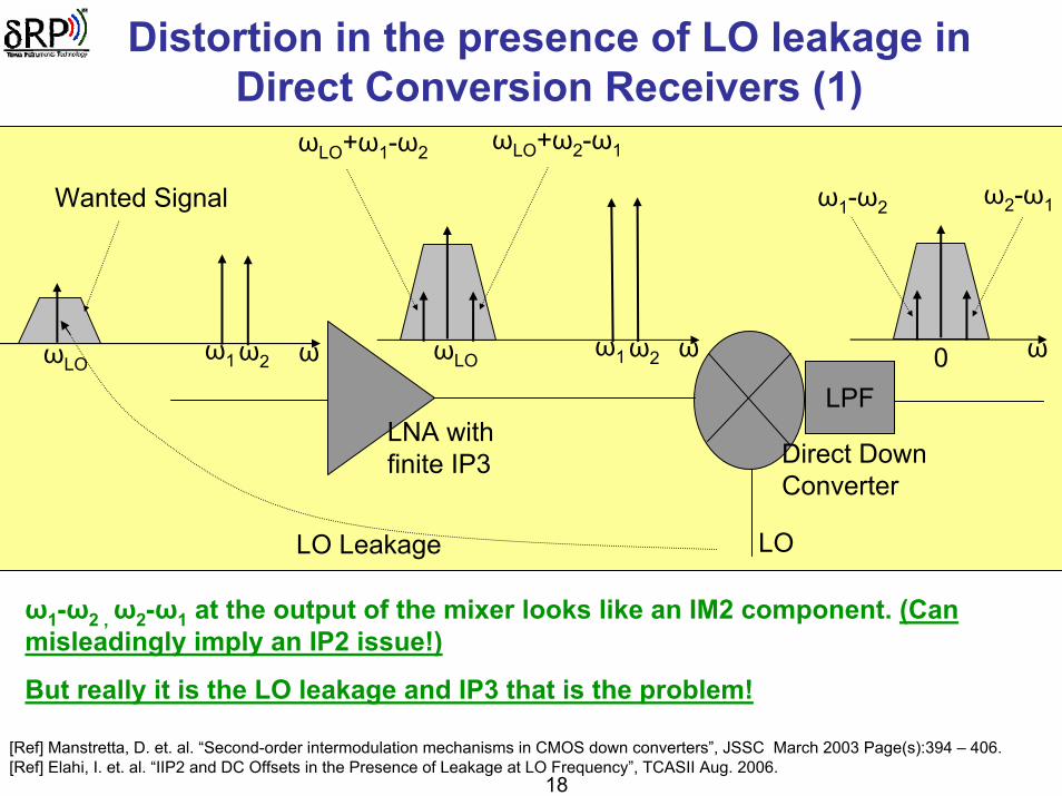
Distortion in the presence of LO leakage in Direct Conversion Receivers (1)
ω1-ω2 , ω2-ω1 at the output of the mixer looks like an IM2 component. (Can misleadingly imply an IP2 issue!)
But really it is the LO leakage and IP3 that is the problem!
LO
ω1ω2ωLOω1ω2ωLOω ω ω0
ωLO+ω2-ω1ωLO+ω1-ω2
ω2-ω1ω1-ω2
Direct Down Converter
LNA with finite IP3
LO Leakage
LPF
Wanted Signal
[Ref] Manstretta, D. et. al. “Second-order intermodulation mechanisms in CMOS down converters”, JSSC March 2003 Page(s):394 – 406.[Ref] Elahi, I. et. al. “IIP2 and DC Offsets in the Presence of Leakage at LO Frequency”, TCASII Aug. 2006.
19
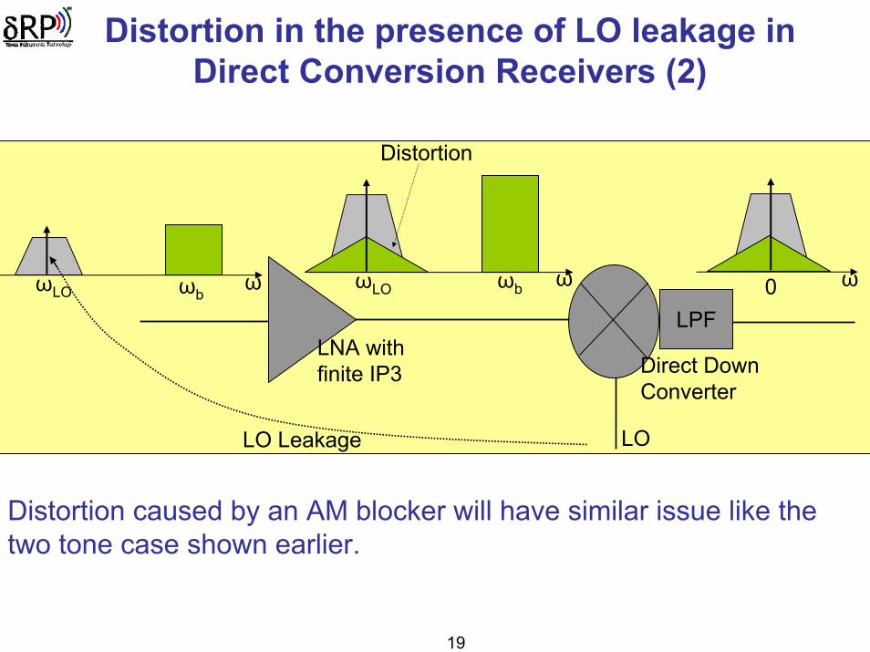
Distortion in the presence of LO leakage in Direct Conversion Receivers (2)
Distortion caused by an AM blocker will have similar issue like the two tone case shown earlier.
LO
ωbωLO ωbωLOω ω ω0
Direct Down Converter
LNA with finite IP3
LO Leakage
LPF
Distortion
20
Performance re-configurability in RF front end
A high dynamic range RF Front End design without any inter-stage external filter is the starting point.
Need to be able to program this front end for various combinations of noise/linearity/power.
Need to have little degradation in overall performance between various programming modes.
High Linearity mode – FDD mode, higher input signal conditions.
Low Noise mode – TDD mode, sensitivity conditions.
Low Power mode – high input signal, low level of blockers.
Linearity/(Noise*Power) ~ Constant
21
Outline
• The need for highly reconfigurable “multi-band, multi-mode”SDR receiver.
• Multi-band receiver: Design directions and challenges.
• Multi-mode receiver: Architecture and design strategy for a re-configurable receiver.
• A WCDMA, GSM/EDGE “multi-mode” RF receiver front-end in 90nm CMOS.
• Conclusion.
22
A WCDMA, GSM/GPRS/EDGE “multi-mode” RF Receiver Front End in 90nm CMOS without inter-
stage SAW filter
23
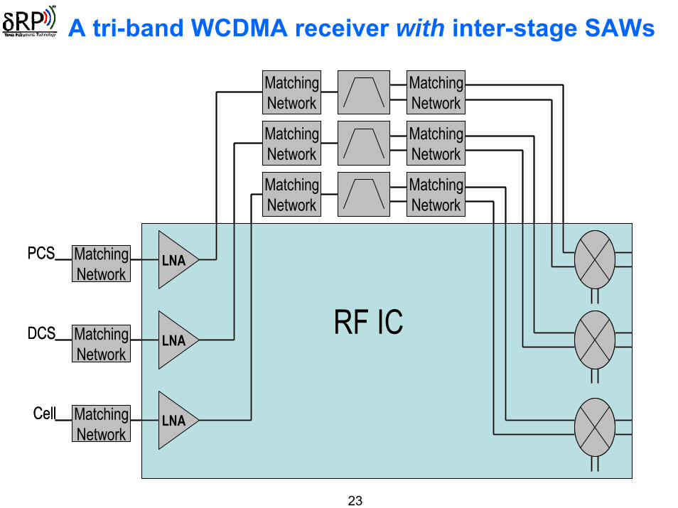
A tri-band WCDMA receiver with inter-stage SAWs
LNAMatchingNetwork
MatchingNetwork
LNAMatchingNetwork
LNAMatchingNetwork
MatchingNetwork
MatchingNetwork
MatchingNetwork
MatchingNetwork
MatchingNetwork
PCS
DCS
Cell
RF IC
LNAMatchingNetwork
MatchingNetwork
LNAMatchingNetwork
LNAMatchingNetwork
MatchingNetwork
MatchingNetwork
MatchingNetwork
MatchingNetwork
MatchingNetwork
PCS
DCS
Cell
RF IC
24
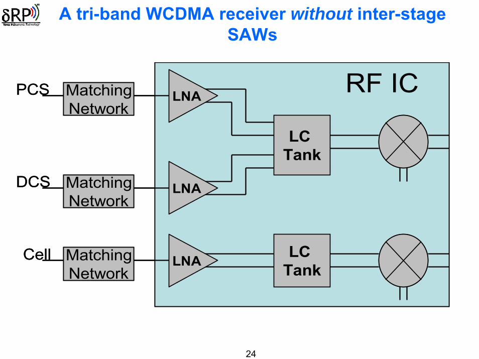
A tri-band WCDMA receiver without inter-stage SAWs
MatchingNetwork
MatchingNetwork
MatchingNetwork
LC Tank
LNA
LNA
LC TankLNA
PCS
DCS
Cell
RF ICMatchingNetwork
MatchingNetwork
MatchingNetwork
LC Tank
LNA
LNA
LC TankLNA
PCS
DCS
Cell
RF IC
25
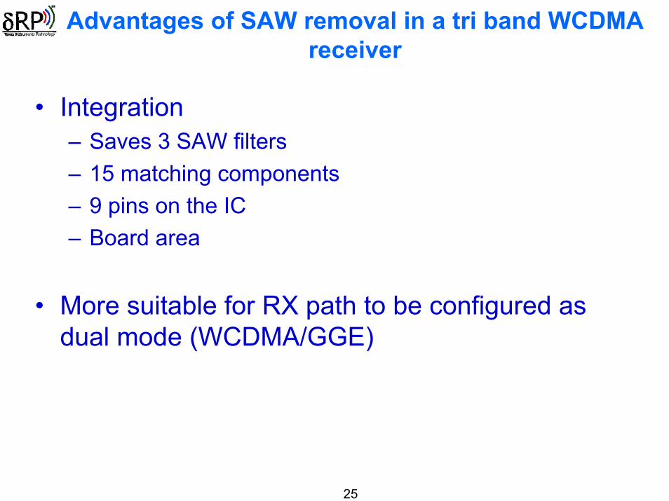
Advantages of SAW removal in a tri band WCDMA receiver
• Integration– Saves 3 SAW filters– 15 matching components– 9 pins on the IC– Board area
• More suitable for RX path to be configured as dual mode (WCDMA/GGE)
26
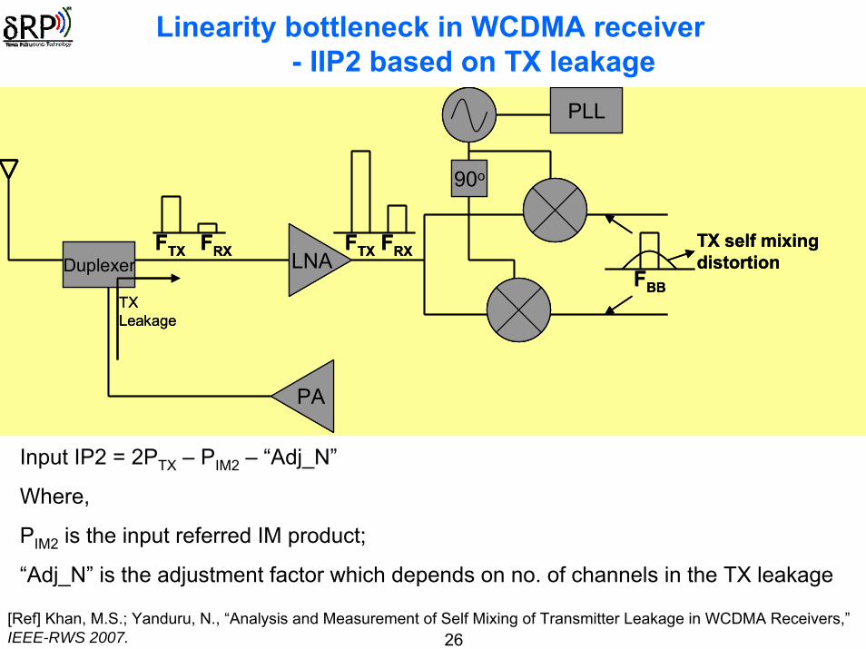
Linearity bottleneck in WCDMA receiver- IIP2 based on TX leakage
LNADuplexer
PA
PLL
90o
TX Leakage
TX self mixing distortion
FTX FRX FRXFTX
FBB
LNADuplexer
PA
PLL
90o
TX Leakage
TX self mixing distortion
FTX FRX FRXFTX
FBB
Input IP2 = 2PTX – PIM2 – “Adj_N”
Where,
PIM2 is the input referred IM product;
“Adj_N” is the adjustment factor which depends on no. of channels in the TX leakage
[Ref] Khan, M.S.; Yanduru, N., “Analysis and Measurement of Self Mixing of Transmitter Leakage in WCDMA Receivers,”IEEE-RWS 2007.
27
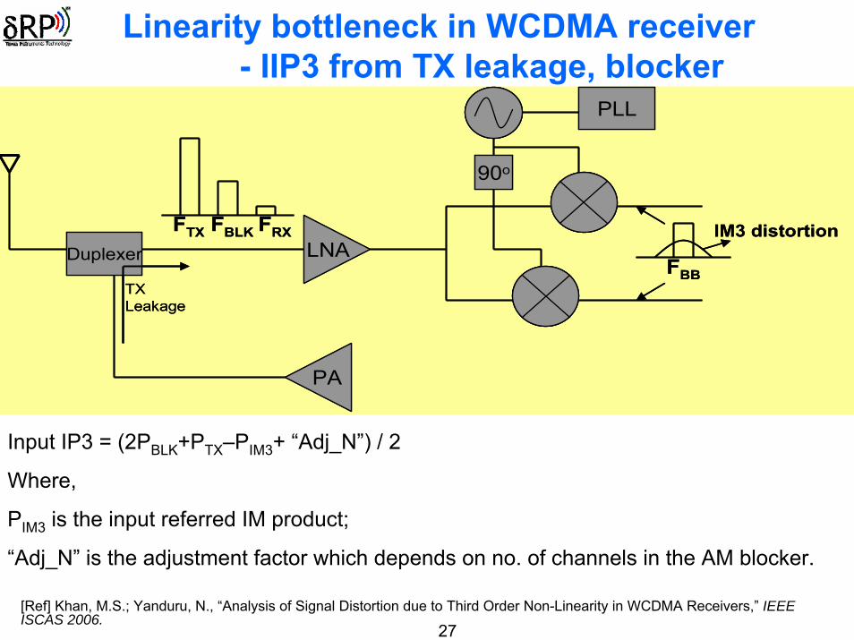
Linearity bottleneck in WCDMA receiver- IIP3 from TX leakage, blocker
LNADuplexer
PA
PLL
90o
TX Leakage
IM3 distortionFTX
FBB
FBLK FRXLNADuplexer
PA
PLL
90o
TX Leakage
IM3 distortionFTX
FBB
FBLK FRX
Input IP3 = (2PBLK+PTX–PIM3+ “Adj_N”) / 2
Where,
PIM3 is the input referred IM product;
“Adj_N” is the adjustment factor which depends on no. of channels in the AM blocker.
[Ref] Khan, M.S.; Yanduru, N., “Analysis of Signal Distortion due to Third Order Non-Linearity in WCDMA Receivers,” IEEE ISCAS 2006.
28
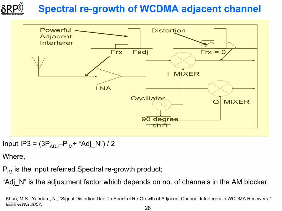
Spectral re-growth of WCDMA adjacent channel
Input IP3 = (3PADJ–PIM+ “Adj_N”) / 2
Where,
PIM is the input referred Spectral re-growth product;
“Adj_N” is the adjustment factor which depends on no. of channels in the AM blocker.
Khan, M.S.; Yanduru, N., “Signal Distortion Due To Spectral Re-Growth of Adjacent Channel Interferers in WCDMA Receivers,”IEEE-RWS 2007.
29
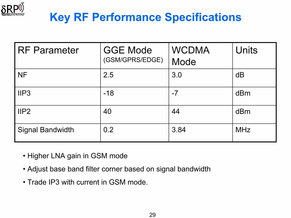
Key RF Performance Specifications
RF Parameter GGE Mode (GSM/GPRS/EDGE)
WCDMA Mode
Units
NF 2.5 3.0 dB
IIP3 -18 -7 dBm
IIP2 40 44 dBm
Signal Bandwidth 0.2 3.84 MHz
• Higher LNA gain in GSM mode
• Adjust base band filter corner based on signal bandwidth
• Trade IP3 with current in GSM mode.
30
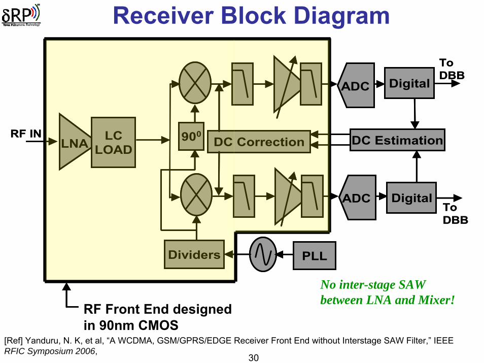
Receiver Block Diagram
Digital
DC Estimation
ADC
LNA LCLOAD
Dividers
DC Correction
ADC
PLL
900RF IN
To DBB
To DBB
Current Chip Presented
Digital
Digital
DC Estimation
ADC
LNALNA LCLOAD
Dividers
DC Correction
ADCADC
PLL
900RF IN
To DBB
To DBB
Current Chip Presented
Digital
RF Front End designed in 90nm CMOS
No inter-stage SAW between LNA and Mixer!
[Ref] Yanduru, N. K, et al, “A WCDMA, GSM/GPRS/EDGE Receiver Front End without Interstage SAW Filter,” IEEE RFIC Symposium 2006,
31
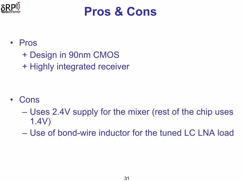
Pros & Cons
• Pros+ Design in 90nm CMOS+ Highly integrated receiver
• Cons – Uses 2.4V supply for the mixer (rest of the chip uses
1.4V)– Use of bond-wire inductor for the tuned LC LNA load
32
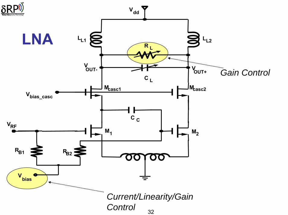
LNA R L
VOUT+
Mcasc1
VRF
RB1
M1
Vbias
Vbias_casc
Vdd
C L
VOUT-
M2
Mcasc2
LL1 LL2
RB2
C C
Gain Control
Current/Linearity/Gain Control
33
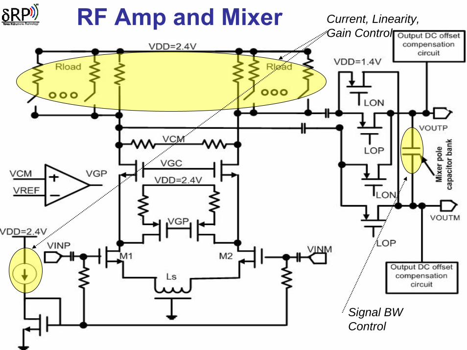
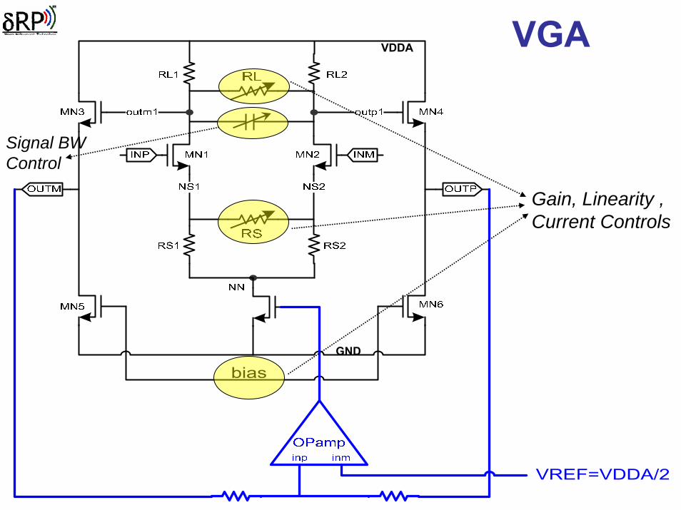
RF Amp and Mixer Current, Linearity, Gain Control
Signal BW Control
34
GND
VDDA VGA
Gain, Linearity , Current Controls
Signal BW Control
35
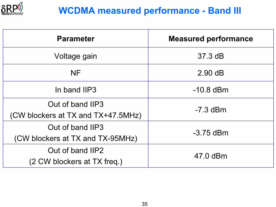
WCDMA measured performance - Band III
Parameter Measured performance
37.3 dB
2.90 dB
-10.8 dBm
-7.3 dBm
-3.75 dBm
47.0 dBm
Voltage gain
NF
In band IIP3
Out of band IIP3(CW blockers at TX and TX+47.5MHz)
Out of band IIP3(CW blockers at TX and TX-95MHz)
Out of band IIP2(2 CW blockers at TX freq.)
36
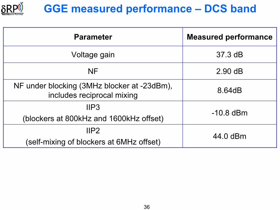
GGE measured performance – DCS band
Parameter Measured performance
37.3 dB
2.90 dB
NF under blocking (3MHz blocker at -23dBm), includes reciprocal mixing 8.64dB
-10.8 dBm
44.0 dBm
Voltage gain
NF
IIP3(blockers at 800kHz and 1600kHz offset)
IIP2(self-mixing of blockers at 6MHz offset)

37
More Measured performance
Parameter Measured performance
-14 dB
50 uV
Gain imbalance (WCDMA) 0.4 dB
Phase imbalance (WCDMA) 4o
Phase Imbalance (GGE) 1o
Out of Band IIP2 (WCDMA)(CW blockers at RX+TX and TX)
34.7 dBm
0.3 dB
S11
Output DC offset (after correction)
Gain Imbalance (GGE)
38
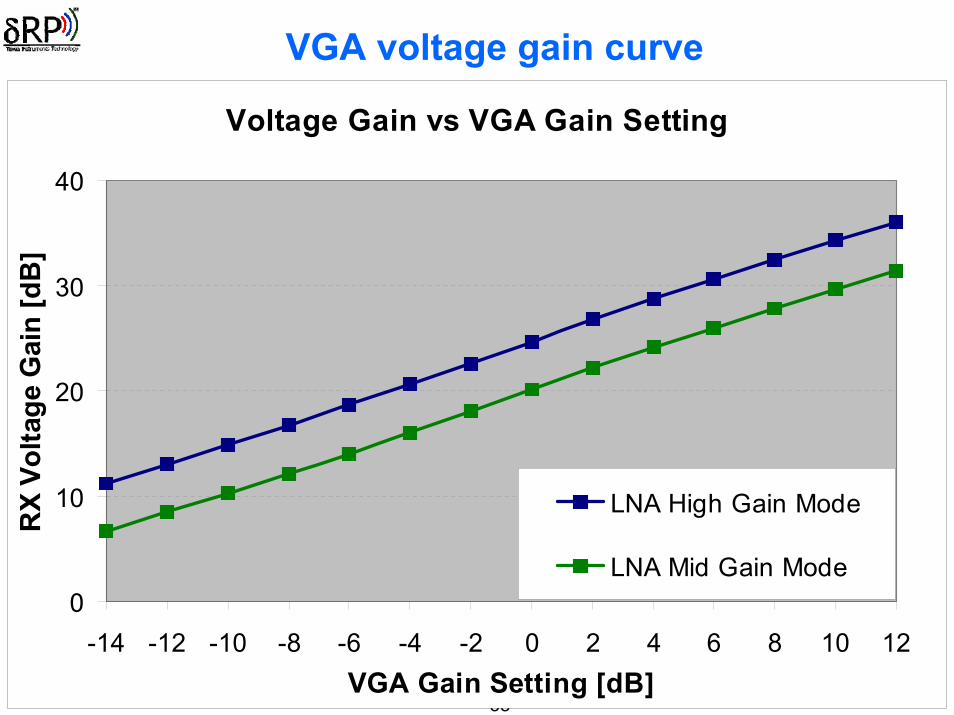
VGA voltage gain curve
Voltage Gain vs VGA Gain Setting
0
10
20
30
40
-14 -12 -10 -8 -6 -4 -2 0 2 4 6 8 10 12VGA Gain Setting [dB]
RX
Volta
ge G
ain
[dB
]
LNA High Gain Mode
LNA Mid Gain Mode
39
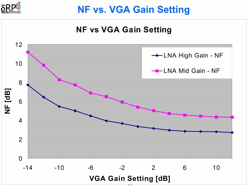
NF vs. VGA Gain Setting
NF vs VGA Gain Setting
0
2
4
6
8
10
12
-14 -10 -6 -2 2 6 10
VGA Gain Setting [dB]
NF
[dB
]
LNA High Gain - NF
LNA Mid Gain - NF
40
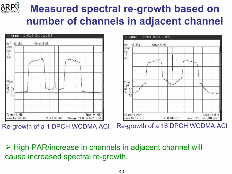
Measured spectral re-growth based on number of channels in adjacent channel
Re-growth of a 16 DPCH WCDMA ACIRe-growth of a 1 DPCH WCDMA ACI
High PAR/increase in channels in adjacent channel will cause increased spectral re-growth.
41
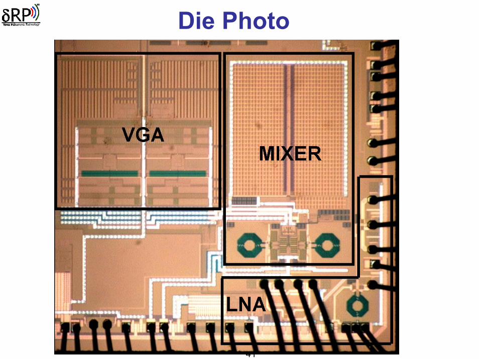
Die Photo
42
Outline
• The need for highly reconfigurable “multi-band, multi-mode”SDR receiver.
• Multi-band receiver: Design directions and challenges.
• Multi-mode receiver: Architecture and design strategy for a re-configurable receiver.
• A WCDMA, GSM/EDGE “multi-mode” RF receiver front-end in 90nm CMOS.
• Conclusion.
43
Conclusion
The need for “multi-band, multi-mode” receivers to support SDR is highlighted.
Multi-band receiver: Various approaches and directions in trying to achieve this goal are presented.
Multi-mode receiver: A multi-mode receiver front end in 90nm CMOS is presented.The high performance achieved eliminates the need for inter-stage SAW filter.
Once a clear winner showing the performance and requirements for multi-band receiver emerges, we will have the RF receiver for SDR.
44
Acknowledgements
• Danielle Griffith• Kah-Mun Low• CC Chen• Fikret Dulger• Sudhind Dhamankar
45
References
• Kuhn, W.B.; Yanduru, N.K.; Wyszynski, A.S., “Q-enhanced LC bandpass filters for integrated wireless applications”, Microwave Theory and Techniques, IEEE Transactions on, Vol. 46, Issue: 12 , Dec. 1998.
• W.B. Kuhn, “Fully integrated bandpass filters for wireless transceivers-problems and promises” MWSCAS-2002, Volume 2, 4-7 Aug. 2002 Page(s):II-69 - II-72 vol.2
• Nguyen C. T –C, “RF MEMS in wireless Architectures”, DAC 2005, June 13 -17 2005, Page(s): 416 – 420.• S.-J Park, K.-Y Lee, G.M. Rebeiz, “Low-Loss 5.15 to 5.70-GHz RF MEMS Switchable Filter for Wireless LAN Applications”
IEEE Transactions on Microwave Theory and Techniques, Vol 54, Issue 11, Nov. 2006 Page(s):3931 – 3939.• Muhammad, K., et al, “The First Fully Integrated Quad-Band GSM/GPRS Receiver in a 90-nm Digital CMOS Process” Solid-
State Circuits, IEEE Journal of, Vol. 41, Issue 8, Aug. 2006 Page(s):1772 – 1783.• Abidi, A. A., “Evolution of a Software-Defined Radio Receiver’s RF Front End,” RFIC Symposium 2006, Page(s):27 – 30.• R. Gharpurey, S. Ayazian, “Feedforward Interference Cancellation in Narrow-Band Receivers” 2006 IEEE Dallas/CAS
Workshop, Oct. 2006 Page(s):67 – 70.• H. Darabi, “A Blocker Filtering Technique for Wireless Receivers”, ISSCC 2007, Page(s):84 - 85 Vol. 1• Khan, M.S.; Yanduru, N., “Analysis and Measurement of Self Mixing of Transmitter Leakage in WCDMA Receivers,”
RAWCON 2007.• Khan, M.S.; Yanduru, N., “Analysis of Signal Distortion due to Third Order Non-Linearity in WCDMA Receivers,” IEEE
ISCAS 2006.• Khan, M.S.; Yanduru, N., “Signal Distortion Due To Spectral Re-Growth of Adjacent Channel Interferers in WCDMA
Receivers,” RAWCON 2007.• Yanduru, N. K, et al, “A WCDMA, GSM/GPRS/EDGE Receiver Front End without Interstage SAW Filter,” RFIC Symposium
2006, Page(s):19 – 22.• P. Fontaine, A.N. Mohieldin, A. Bellaouar, “A low-noise low-voltage CT Delta Sigma modulator with digital compensation of
excess loop delay” ISSCC 2005, 6-10 Feb. 2005 Page(s):498 - 613 Vol. 1• Ali Ahmad W. Y., “Effective IM2 estimation for two-tone and WCDMA modulated blockers in zero-IF receivers”, RF Design,
April 2004.• Khan, M.S.; Yanduru, N., “Analysis of self mixing of transmitter interference in WCDMA receivers,” ISCAS 2006.
Proceedings. 2006 IEEE International Symposium on; 21-24 May 2006 Page(s):4 pp.• Manstretta, D.; Brandolini, M.; Svelto, F., “Second-order intermodulation mechanisms in CMOS down converters”, Solid-
State Circuits, IEEE Journal of, Volume 38, Issue 3, March 2003 Page(s):394 – 406.• Elahi, I.; Muhammad, K.; Balsara, P.T., “IIP2 and DC Offsets in the Presence of Leakage at LO Frequency”, IEEE
Transactions on Circuits and Systems II: Express Briefs, Volume 53, Issue 8, Aug. 2006 Page(s):647 – 651.• Craninckx, J, et al, “A Fully Reconfigurable Software-Defined Radio Transceiver in 0.13μm CMOS,” IEEE ISSCC 2007