Embed Size (px)
Citation preview

CER
N-T
HES
IS-2
013-
274
31/0
8/20
13
Design and Control of Modular Multilevel Converter in an Active Front End
Application
Master of Science Thesis in Electric Power Engineering
Panagiotis Asimakopoulos
Department of Energy and Environment
Division of Electric Power Engineering
CHALMERS UNIVERSITY OF TECHNOLOGY
Göteborg, Sweden, 2013

ii

iii
“Design and Control of Modular Multilevel Converter in an Active Front End Application”
By
Panagiotis Asimakopoulos
This Thesis was elaborated during a Technical Training Programme at CERN, the European
Laboratory for Particle Physics.

iv
Supervisor
Konstantinos Papastergiou
Technology Department
European Laboratory for Particle Physics (CERN)
Examiner
Massimo Bongiorno
Associate Professor, Chalmers University of Technology
Department of Energy and Environment
Division of Electric Power Engineering
CHALMERS UNIVERSITY OF TECHNOLOGY
Göteborg, Sweden, 2013

v
DESIGN AND CONTROL OF MODULAR MULTILEVEL CONVERTER IN AN
ACTIVE FRONT END APPLICATION
PANAGIOTIS ASIMAKOPOULOS
©PANAGIOTIS ASIMAKOPOULOS, 2013
Department of Energy and Environment
Division of Electric Power Engineering
CHALMERS UNIVERSITY OF
TECHNOLOGY
SE-412 96 Göteborg
Sweden
Telephone: + 46 (0)31-772 1000
Göteborg, 2013
Electrical Power Converters Group
TECHNOLOGY DEPARTMENT
EUROPEAN LABORATORY
FOR PARTICLE PHYSICS
CERN, 1211 Geneva
Switzerland


vii
Design and Control of Modular Multilevel Converter in an Active Front End Application
PANAGIOTIS ASIMAKOPOULOS
Department of Energy and Environment
Division of Electric Power Engineering
Chalmers University of Technology
ABSTRACT
In CERN, the European Organization for Nuclear Research, the particles’ accelerators
demand controlled magnetic fields for the particles move. The necessary magnetic fields are
achieved by supplying electromagnets with current precisely controlled by power electronics.
The magnets are supplied with dc current and a diode rectifier circuit or a more advanced
Active Front End converter is used for the connection with the grid.
The Active Front End converters offer the possibility to control both sides of the circuit, the
ac and the dc side. In this way, the ac side current can be controlled to approach the
sinusoidal waveform and to avoid the reactive power flow. At the same time the dc-link
voltage can be regulated.
A proposed topology to operate as an Active Front End is the Modular Multilevel Converter.
The Modular Multilevel Converter is a new solution in the field of medium and high power
electronics. The converter’s operation is based on the modular approach. It consists of
modules, each one being a half-bridge connected in parallel to a capacitor. The special
characteristic of this idea is that it is possible to build the sinusoidal waveform of the voltage
by adding several modules in series in each phase-leg of the converter. An arm inductance is
connected in series with the modules of every arm. In contrast to the two level voltage source
converter, where the output phase voltage can be either plus or minus the half of the dc-link
voltage, the MMC can change its output with steps equal to each module capacitor’s voltage
level.
Some features of the converter that are interesting especially for this application are:
i. the redundancy in operation due to the several modules used in each arm that is
very important for experiments running for long periods of time and being difficult
to interrupt in case of failure.

viii
ii. the probable reduction in the cost for the medium voltage level application due to
the lower ratings of the switches in each module
iii. the sinusoidal waveforms with very low harmonic content that reduce drastically
the size of the filters used in the input of the converter.
iv. Low switching frequency of the semiconductors, typically up to 20 times the
fundamental
In this work, the appropriateness of the Modular Multilevel Converter is investigated. At the
beginning, the operation of the topology is analyzed and the extra considerations are pointed
out. A feature of this topology is the significant second harmonic component of the current
that circulates among the phase legs and mainly increases the losses. Secondly, the sizing
process for the module capacitance and the arm inductance is described. A stepwise design
procedure is presented for the total system, starting from the magnet specifications, the dc-
link capacitance and voltage choice, the converter and the transformer ratings. Subsequently,
the suitable control strategy is selected.
The existence of the modules capacitors necessitates the control of their voltage level. A
dedicated controller is described that has two main parts; the averaging controller that takes
care of the average capacitor voltage level per leg and the balancing controller that regulates
the voltage of each capacitor separately. In this application the load is well specified and the
dc-link voltage of the converter can be assigned to the averaging controller. The power flow
control and the grid current quality are assigned to an ac current controller.
Keywords: Modular multilevel Converter, Control system, Active Front End, Pulsed
Power Applications

ix
ACKNOWLEDGEMENTS
This master thesis was carried out at the Medium Power Converters section of the Electrical
Power Converters group. This group is a part of the Technology Department at CERN.
I would like to express my gratitude to my supervisor Konstantinos Papastergiou, researcher
at the Medium Power Converters section, for giving me the opportunity to work on this very
interesting project at the scientific environment of CERN. His continuous academic and
technical guidance and our friendly personal contact are very valuable for me. I would also
like to thank my examiner from Chalmers University of Technology, Massimo Bongiorno for
the very useful feedback and the interesting conversations during our meetings. I am thankful
to Stefan Lundberg, researcher and Torbjorn Thiringer, professor, both from Chalmers
University of Technology for their support during my master thesis selection process.
My working experience at the Medium Power Converters section was challenging but also
very pleasant. Special thanks to the section leader Gilles Le Godec for offering me technical
knowledge and practical comments during the project. Generally, many thanks to all my
colleagues in Medium Power Converters section and High Power Converters section for
accepting me very kindly as a member.
My deepest gratefulness goes to my family for their continuous support and patience during
my life.
Panagiotis Asimakopoulos
Prevessin, France, June 2013

x
NOMENCLATURES
MMC Modular Multilevel Converter
AFE Active Front End
NPC Neutral Point Clamped
EMI Electromagnetic Interference
FFT Fast Fourier Transformation
IGBT Insulated Gate Bipolar Transistor
HVDC High Voltage Direct Current
Arm inductor voltage
DC-link voltage
Load voltage
DC-link power
Load power
Dc-link current
Load current
Number of modules per arm
Number of modules per leg
Current direct axis
Current quadrature axis
Arm current
Second harmonic filter inductance
Second harmonic filter capacitance
Fundamental angular frequency
s Second
A Ampere
V Volts
W Watt
Per unit
Capacitor charge
Coulomb
Capacitor ripple
Switching frequency
PWM Pulse Width Modulation
SPWM Sinusoidal Pulse Width Modulation

xi
SVM Space Vector Modulation
PI Proportional –Integral controller
Arm inductance
Arm resistance
THD Total Harmonic Distortion
Load voltage
Module voltage
Upper arm current
Lower arm current
Circulating current
Line impedance
Phase shift between two sources
PLL Phase Locked Loop
Magnet inductance
Magnet resistance
Magnet pulsing period
Magnet power
Magnet voltage
Magnet current
Maximum magnet current
DC-link Capacitor time constant
H-bridge current
H-bridge efficiency
DC-link minimum voltage
DC-link initial voltage
Magnet inductance maximum energy
Capacitor energy
Magnet ohmic losses
Converter voltage
Grid voltage
Maximum magnet ohmic losses
IMC Internal Model Control
Current controller bandwidth
Ohm
Farrad
Integral controller gain
Proportional controller gain
Equivalent switching frequency
Damping resistance

xii
Controller transfer function
Physical system transfer function
Closed loop transfer function
Converter voltage in dq coordinates
Complex integrator state variable
Half of the arm resistance
Half of the arm inductance
Complex integrator state variable in dq
coordinates
Derivative of the complex integrator state
variable in dq coordinates
Limited derivative of the complex integrator
state variable in dq coordinates
Current controller output in dq coordinates
Limited current controller output in dq
coordinates
Module capacitance
DC-link capacitance
rms Root mean square value
Peak load current
dq Direct quadrature
Transformer leakage inductance
Secondary winding transformer rms phase
voltage
Secondary winding transformer rms current
Short-circuit impedance of the transformer

xiii
LIST OF FIGURES
Figure 1.1: CERN particle accelerators' chain 1
Figure 1.2: MMC topology 2
Figure 1.3: MMC control general overview 2
Figure 2.1: 1-phase MMC 5
Figure 2.2: Switch operation inside the MMC module 6
Figure 2.3: MMC equivalent model 6
Figure 2.4: Load voltage 8
Figure 2.5: Inner alternating voltage of the converter 9
Figure 2.6: Phase equivalent circuit 9
Figure 2.7: Capacitor voltage 10
Figure 2.8: Common mode voltage 11
Figure 2.9: Differential mode voltage 12
Figure 2.10: Three-phase MMC with the dominant currents flowing in the arms: Ia Ib, Ic the
load currents, I2 the second harmonic component and Idc the dc-component of the
circulating current
13
Figure 2.11: Different structures of the explosion proof housing 14
Figure 2.12: Full-bridge module 15
Figure 2.13: Clamp-double module 15
Figure 3.1: 1-phase MMC 17
Figure 3.2: Upper arm current for different number of modules per arm 18
Figure 3.3: From top to bottom: load current, upper arm current, lower arm current, modules’
output voltage- voltage - In the fourth plot the significant difference in the voltage
amplitudes is just a change in plotting for clarity.
19
Figure 3.4: Upper arm current for N=10 20
Figure 3.5: Fault at dc-link for half-bridge module 21
Figure 3.6: From top to bottom: Phase currents and modules capacitors' voltage 22
Figure 3.7: From top to bottom: Phase currents and modules capacitors' voltage. 22
Figure 3.8: Fault at dc-link for full-bridge module 23
Figure 3.9: Second order harmonic suppression filter
Figure 3.10: Upper capacitor voltage ripple, upper arm current and upper module output
voltage
24
25
Figure 3.11: Upper capacitor voltage ripple for different N 27
Figure 4.1: Phase disposition PWM 29
Figure 4.2: Phase opposition disposition PWM 30
Figure 4.3: Alternative phase opposition disposition PWM 30
Figure 4.4: Phase-shifted PWM 30

xiv
Figure 4.5: Voltage balancing control with phase shifted PWM 32
Figure 5.1: System equivalent circuit 35
Figure 5.2: Examples of modes of operation for VSC 36
Figure 5.3: Theoretical P-Q capability diagram for VSC 36
Figure 5.4: Thyristor bridges 37
Figure 5.5: Diode rectifier and H-bridge 37
Figure 5.6: Two level VSC and H-bridge 37
Figure 5.7: Diode rectifier, boost converter and H-bridge. 38
Figure 5.8: VSC control overview. 39
Figure 6.1: Magnet current specification – Current value as a function of time for the 0.9 s
period 41
Figure 6.2: Complete structure of the system 42
Figure 6.3: Analytical model used at the simulation for the combination of the magnet and the
H-bridge 43
Figure 6.4: Load for each semiconductor depending on the arm current sign 44
Figure 6.5: Upper switch current (light green), lower switch current (blue) and upper arm
current (dark green) during a magnet cycle of 0.9 s 45
Figure 6.6: : Upper diode current (light green), lower diode (blue) current and upper arm
current (dark green)during magnet cycle of 0.9 s 45
Figure 6.7: General overview of the current controller and the physical system 49
Figure 6.8: Block diagram with the real physical system 50
Fi Figure 6.9: Simplified block diagram 50
Figure 6.10: Feed forward of coupling term and grid voltage 52
Figure 6.11: Complete current controller 53
Figure 6.12: Current controller reference calculation 54
Figure 6.13: Voltage balancing control 55
Figure 6.14: Control structure overview 56
Figure 7.1: Simulation results overview for N=4 57
Figure 7.2: Grid current for N=4 59
Figure 7.3: Converter output phase voltage for N=4 59
Figure 7.4: Simulation results overview for N=6 60
Figure 7.5: Grid current for N=6 61
Figure 7.6: Converter output phase voltage for N=6 61
Figure 7.7: Operation overview for N=10 and fsw=1000 Hz 62
Figure 7.8: Grid current for N=10 and fsw= 1000Hz 63
Figure 7.9: Converter output phase voltage for N=10 and fsw=1000 Hz 63

xv
Figure 7.10: Simulation results overview for N=10 and fsw=350 Hz 64
Figure 7.11: Grid current for N=10 and fsw=350 Hz 65
Figure 7.12: Converter output phase voltage for N=10 and fsw=350 Hz 65
Figure A.1: Model overview 75
Figure A.2: Current controller of id component 76
Figure A.3: Voltage balancing controller overview 76
Figure A.4: Capacitor's individual voltage balancing controller 77
Figure A.5: Averaging controller 77
Figure A.6: One phase-leg 78
Figure A.7: Module
Figure A.8: Load model-Magnet and H-bridge simulation model
Figure A.9: Current controller reference calculation
79
79
80

xvi
LIST OF TABLES
Table 1.1: Advantages and disadvantages of the MMC 3
Table 2.1: One capacitor voltage FFT 10
Table 2.2: Sum of two capacitors’ voltages in the upper arm FFT 11
Table 2.3: Circulating current FFT 12
Table 5.1: Topologies used at CERN 38
Table 6.1: Load specifications 42
Table 6.2: Semiconductors’ rms and peak current values 46
Table 6.3: Current controller parameters for N=4
Table 6.4: Average and balancing controller gains for N=4
54
55
Table 7.1: Converter parameters for N=4 58
Table 7.2: Converter parameter for N=6 59
Table 7.3: Converter parameters for N=10, fsw=1 kHz 61
Table 7.4: Converter parameters for N=10, fsw=350 Hz 63
Table 7.5: Summary of THD for different N and switching frequency 65
Table A.1: Types of transformation 74

xvii
TABLE OF CONTENTS
ABSTRACT…………………………………………………………………………….....vii
ACKNOWLEDGEMENTS………………………………………………………………..ix
NOMENCLATURES………………………………………………………………………x
LIST OF FIGURES……………………………………………………………………....xiii
LIST OFTABLES……………………………………………………………………….. xvi
TABLE OF CONTENTS………………………………………………………………...xvii
Chapter1. Introduction………………………………………………………………………...1
1.1 Background…………………………………………………………………..….......1
1.2 The Modular Multilevel Converter……………………………………………..…...2
1.3 Aim…………………………………………………………………………….…….4
1.4 Thesis outline…………………………………………………………………….….4
Chapter 2. Operation and analysis of the Modular Multilevel Converter……………..............5
2.1 Physical structure of the 1-phase Modular Multilevel Converter…….....…….……..5
2.2 Operation of the 1-phase Modular Multilevel Converter…………………………....6
2.3 Circulating current……………………………………………………………….…..9
2.4 Dc-link fault and non-controllable addressing………………………………….…..13
2.5 Limitation of dc-link fault currents by modules structure and control………….….14
Chapter 3. Components dimensioning…………………………………………………….....17
3.1. The role of the arm inductance…………………………………………..................17
3.2 Second-order harmonic suppression filter................................................……….…23
3.3 Module capacitance dimensioning………………………………………………....24
Chapter 4.Voltage balancing control strategies and modulation techniques…………….…..29
4.1 Modulation techniques………………………………………………………….….29
4.1.1 Sinusoidal Pulsed Width Modulation……………………………………………...29
4.1.2 Active selection process………………………………………………………...31
4.2 Voltage balancing control methods…………………………………………….…..31
4.2.1. Voltage balancing control with phase shifted PWM modulation…....................31
4.2.2 Closed-loop control…………………………………………………………......32
4.2.3 Open-loop control…………………………………………………….….….….32
4.3 The applied voltage balancing control method and modulation technique………..33
Chapter 5. Active Front End operation and control of Voltage Source Converters……........35
5.1 Principles of power control for a VSC and AFE operation ………………..……...35

xviii
5.2 Examples of topologies used as AFE converters for magnet supply at CERN…….36
5.3 Control of AFE converters…………………………………………………………38
Chapter 6. Converter design procedure………………………………………………..……..41
6.1 Load specifications……………………………………………………………........41
6.2 Sizing of dc-link capacitor…………………….…………………….………….…..43
6.3 MMC power and components ratings…………………….…………….…………..43
6.3.1. Semiconductors ratings ………………………………………………...........…44
6.3.2 Module capacitance dimensioning ……………………………………….….....46
6.3.3 Arm inductance dimensioning…………………………………….........….........47
6.3.4 Selection for the number of modules per arm…………………………….…....48
6.4 Transformer ratings…….……….……….……….……….……….…….….……...49
6.5 Controllers definition and design…….……….……….……….……….….………49
6.5.1 Current controller design…….………………………………………….….……....49
6.5.2 Controller of dc-link voltage................................................................................54
Chapter 7. Simulation and Results...........................................................................................57
7.1 Simulation model.......................................................................................................57
7.2 Simulation results......................................................................................................57
Chapter 8. Conclusions and future work..................................................................................67
8.1 Conclusions................................................................................................................67
8.2 Future work................................................................................................................68
References................................................................................................................................69
Bibliography.............................................................................................................................70
Appendices ........................................ .......................................................................................73
A.1. Clarke transformation.................................................................................................73
A.2. Park transformation....................................................................................................74
A.3. Total Harmonic Distortion.........................................................................................74
A.4. Simulink model..........................................................................................................75

xix

xx

Chapter 1
Introduction 1.1 Background
CERN, the European Organization for Nuclear Research, conducts research open to international
co-operation in the field of physics concerning high-energy particles. To this direction, special
attention is paid to the design of the equipment supporting the experiments.
The particles’ acceleration necessitates controlled magnetic fields. Power electronics are an
essential component of the experimental setup due to the fact that they control with precision the
current supplied to the electromagnets of the accelerators. The demanding applications of power
electronics in the experiments lead the Electrical Power Converter (EPC) group to further develop
the power electronic converters for future accelerators.
One of the responsibilities of the EPC group is the power supply of the Proton Synchrotron
Booster (PS Booster). PS Booster is a circular accelerator and it accelerates beams of protons from
the energy of 50MeV up to 1.4 GeV. It is a part of the accelerator chain at the CERN Large
Hadron Collider, see figure 1.1. The future upgrade of the PS Booster aims to accelerate the beams
up to the energy of 2 GeV. The load specifications for the upgrade of the PS Booster are used as an
example to test the capability of the converter.
Figure 1.1: CERN particle accelerators' chain
In the framework of future application at CERN, it was proposed to investigate the Modular
Multilevel Converter (MMC) operating as an Active Front End converter. An AFE is a

2
controllable rectifier regulating the dc-link voltage and at the same time keeping the ac side current
quality within the acceptable limits for grid connection.
1.2 The Modular Multilevel Converter
The MMC studied in this work consists of a number of cascaded modules, each one being a half-
bridge connected to a capacitor [1]. Several modules connected in series with an inductance form a
converter arm, according to figure 1.2. Two converter arms form a phase-leg.
E
E
m1R+
mnR+
m1S+
mnS+
m1T+
mnT+
mnR-
m1R-
mnS-
m1S-
mnT-
m1T-
R S T
Figure 1.2. MMC topology
The structure of the MMC including module capacitors indicates that an inner voltage balancing
control for the capacitors’ voltage level is needed. This balancing control includes two parts: the
control of the average capacitor voltage in a leg and an individual voltage control for each of the
modules in the leg. The dc-link voltage control is assigned to this balancing control. Figure 1.3
provides a general picture of the different controls blocks acting at the MMC.
io
ac grid
capacitor voltage balancing control
ac current control
average control
dc-link
Figure 1.3: MMC control general overview

3
Table 1.1 makes a synopsis of the main advantages and disadvantages of the MMC:
Table 1.1:Advantages and disadvantages of the MMC
+ - Low actual switching frequency but high
effective: , where is the number
of modules per leg, therefore significantly
decreasing the switching losses
Vulnerable to faults at dc-link. The lower
antiparallel diodes of the switches in the modules
are forward biased
Stepwise change in the output voltage reducing
the Electromagnetic Interference (EMI)
Need for protection in case of semiconductor failure
in a module. The stored energy in the module
capacitor will be released leading to explosion No need for bulk filters at the ac side (cost and
area saving) due to the low harmonic content of
the current produced
The arm inductance is the converter’s inner filter.
There is also a dc current component through the
filter
Redundancy due to the extra modules that can be
connected to substitute the failed ones
Extra control for the voltage balancing of the
modules’ capacitors is needed Reduction or even elimination of capacitance in
dc-link due to the fact that the energy is stored in
the converter’s modules
Attention for the decoupling of the different
controllers must be paid.
Simple mechanical construction comparing to
other multilevel topologies, e.g. Neutral Point
Clamped (NPC)
Need for monitoring all the capacitors’ voltage
values and (depending on the voltage balancing
method) the arm currents The simple mechanical construction allows to
increase easily the number of levels
Depending on the balancing method the signals of
the capacitors’ and arm currents’ measurements
must be sent to a central processing unit increasing
the needs for data and communication resources Low voltage ratings for semiconductors, very
advantageous for high voltage applications
Circulating current in the phase legs mainly
consisting of second harmonic, which increases the
losses at the components The arm inductance, necessary to limit the current
at the voltage steps, is also used for current
filtering
An extra controller or passive filter may be needed
to suppress the second harmonic in the circulating
current More difficult power stage dimensioning due to the
capacitors, the arm inductors and the circulating
current
For high current applications the voltage drop
across the arm inductance can be significant and can
cause reactive power losses.
In practice, for this application the system consists of the AFE, the dc-link capacitors bank and an
H-bridge converter that further regulates the voltage applied to the load, the magnet. The load can
be modeled as an inductive-ohmic load. It receives periodically current pulses of trapezoidal shape.
The H-bridge together with the magnet is simulated as the total load “seen” by the MMC. The dc-
link capacitor is dimensioned to supply and receive the magnet energy and the AFE is rated to
compensate for the power losses in the magnet.
In fact, the optimal sizing of the converter and the dc-link capacitor voltage level and fluctuation is
a matter of techno-economical analysis. The cost of the capacitor, the ratings and the total cost of
the converter, the price of the energy supplied by the grid and its change through the years as well
as the general construction cost must be taken into consideration. The cost optimization, though
very interesting, is outside of the scope of this thesis.

4
The master thesis is elaborated in collaboration with the Division of Electric Power Engineering in
the Department of Energy and Environment at Chalmers University of Technology.
1.3 Aim
The aim of this master thesis is to:
To examine the state of the art in the MMC design and control
To compile a design guideline for the design sizing of the MMC as an AFE
To evaluate a voltage balancing control method
To evaluate the overall performance of the topology in an AFE application
1. 4 Thesis outline
Chapter 2 explains the operation of the MMC and presents the analysis and the special
considerations for the converter.
Chapter 3 includes a more detailed approach of the converter’s operation and of the sizing of its
components, i.e. the arm inductance, the module capacitance and the semiconductors.
Chapter 4 presents the MMC topology’s inner control dedicated to the voltage balancing of the
modules’ capacitors and the modulation techniques applied.
Chapter 5 describes the AFE operation and control and provides examples of topologies used at
CERN.
Chapter 6 describes the procedure followed for the design of the converter concerning the
calculation of its ratings based on the load specifications. Moreover, the calculation of the ratings
for the converter’s components and the design of the control system is presented.
Chapter 7 presents the results and observations for the system’s simulation.
Chapter 8 includes the conclusions and the suggested future steps as a continuation of this work.

5
Chapter 2
Operation and analysis of the Modular Multilevel Converter
In this chapter, the operation and the mathematical analysis of the MMC are presented. For
simplification, the initial study is based on the 1-phase model and it can be extended to the 3-phase
model. The operation of the 1-phase converter at the inverter mode is explained. The detailed
mathematical analysis is presented, as well as the special considerations for this type of power
electronic converter. Finally, the effect of module failure caused by a dc-link short-circuit and its
addressing are described.
2.1 Physical structure of the 1-phase Modular Multilevel Converter
Figure 2.1 shows the topology of the 1-phase MMC. The converter’s power stage is composed of one
phase leg.
1
2
3
4
Figure 2.1: 1-phase MMC
The main reasons for the utilization of the inductance are summarized in the following bullet points:
Limitation of the current when the dc-link is connected in parallel with one or more modules
taking up a part of the voltage applied to the capacitors.
Replacement of an inductance at the ac side, due to the fact that the arm inductance can
contribute to the ac current filtering.
Limitation of the current in the case of a fault in the dc-link.
Limitation of the current circulating among the legs consisting of higher harmonics, mainly
the second.
Focusing on each module, it consists of a half-bridge with anti-parallel diodes, connected in parallel
with a capacitor. The voltage output of each module is either the capacitor’s voltage, when the

6
capacitor is inserted, or zero, when the capacitor is bypassed. Figure 2.2 illustrates the switch
activated in each possible mode of operation for the module.
iarm iarm
iarm>0 iarm<0 iarm>0
iarm iarm
iarm<0
Figure 2.2: Switch operation inside the MMC module
Conclusively, the topology provides the possibility of energy storage in the arms.
2.2 Operation of the 1-phase Modular Multilevel Converter
In order to understand the basic operation of the converter, it is assumed that the capacitors are
constant DC sources. The arm inductance is ignored.
Vdc/2
Vdc/2
1
2
3
4
Ro
Larm
Larm
Rarm
Rarm
iu
il
io
Vm1
Vm2
Vm3
Vm3
Vo
+-
Figure 2.3: MMC equivalent model
For the upper loop the application of Kirchhoff’s voltage law provides:
and for the lower loop:
where is the load voltage and are the module voltages. According to figure 2.3
the total dc-link voltage is Vdc. The circuit is a three-level converter. The voltage Vo can be
, 0,
.

7
The voltage level of each module is assumed to be equal to
. The potential
can be
achieved by bypassing the two modules at the upper loop and connecting both modules of the lower
loop.
To achieve
, connect both the upper sources and bypass the two lower.
To achieve 0, bypass one module from the upper loop and one from the lower. Hence, there are
four possible ways to have a zero voltage output.
Considering the inductance and its parasitic resistance in each arm:
For the upper loop the Kirchhoff’s voltage law is:
(2.1)
For the lower loop:
(2.2)
The subscripts l and u mean lower and upper respectively and is the load voltage.
The subtraction of (2) from (1) results to:
and
where , the current of the lower and upper loop respectively.
From Kirchhoff’s current law:
where the load current.
(
)
and for the general case of more than 2 modules per arm:
(∑
∑
)
(
)
(2.4)
where N is the number of modules per arm.
For ohmic load the voltage across the load is equal to:

8
Hence, the load current can be written:
(∑
∑
)
(
)
Based on the equations of the aforementioned analysis, it is possible to build a model in
Matlab/Simulink to simulate the basic operation of the converter.
In figure 2.4 the load voltage is shown.
Figure 2.4: Load voltage
It can be noticed that the output voltage, in this case the current too, have 5 levels. As a result, a
waveform with even lower harmonic content is provided. It can be stated that the output phase voltage
of this type of converter has levels from peak to peak including the zero level.
The load phase voltage is expressed as
(2.6)
where are the total voltages of the capacitors inserted in the upper/lower arm.
(2.8) is equivalent to (2.4). It is observed that the load voltage depends on the load current and the arm
voltage difference term
. This term can be considered as the inner alternating voltage output
prior to the arm inductance produced by the converter [1]. The inner alternating voltage is plotted in
figure 2.5 for a three-phase converter with four modules per arm. The current produced is filtered by
the arm inductance to approximate a sinusoidal waveform.

9
Figure 2.5: Inner alternating voltage of the converter
The equivalent circuit for each phase of the converter is presented in figure 2.6. This circuit is helpful
for the design process of the current controller, as it is shown in Chapter 6.
inner voltage
Larm/2Rarm/2
Vo
Figure 2.6: Phase equivalent circuit
2.3 Circulating current
The arm currents can be written based on the sign conventions of figure 2.1 and with the possibility to
extend the analysis to the three-phase case
where j is the phase a, b or c. The part of the arm current not flowing to the load, which is called
circulating current, is defined
10
The circulating current mentioned in [5] consists apparently of a dc component, which is responsible
for the real power flow between the dc-link and the ac side. If higher harmonics connected to the
switching frequency are neglected, the circulating current contains also a significant second harmonic
component, according to [2].
By integrating the instantaneous power flowing in the upper and in the lower arm and summing them
together, the energy stored in a phase leg can be found for a period of time. A dc component and an ac
component of second harmonic occur in the phase leg energy. Due to the fact that the capacitor’s
voltage is related to its stored energy via the equation
(2.8)
it is concluded that the second harmonic in the energy passes through to the capacitor voltage creating
ripple in the module output voltage.
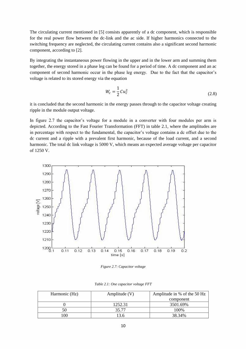
In figure 2.7 the capacitor’s voltage for a module in a converter with four modules per arm is
depicted. According to the Fast Fourier Transformation (FFT) in table 2.1, where the amplitudes are
in percentage with respect to the fundamental, the capacitor’s voltage contains a dc offset due to the
dc current and a ripple with a prevalent first harmonic, because of the load current, and a second
harmonic. The total dc link voltage is 5000 V, which means an expected average voltage per capacitor
of 1250 V.
Figure 2.7: Capacitor voltage
Table 2.1: One capacitor voltage FFT
Harmonic (Hz) Amplitude (V) Amplitude in % of the 50 Hz
component
0 1252.31 3501.69%
50 35.77 100%
100 13.6 38.34%

11
Table 2.2: Sum of two capacitors’ voltages in upper arm FFT
Harmonic (Hz) Amplitude (V) Amplitude in % of the 50 Hz
component
0 2504.3 3504.47%
50 71.47 100%
100 27.51 38.47%
Comparing the results in table 2.1 and table 2.2 the sum of two or more capacitors’ voltages in the
same arm indicates that the second harmonic voltage is very close in phase for the capacitors of the
same arm. The same is valid for the first harmonic.
The sum of all capacitors’ voltages in a phase leg of a converter with four modules per arm called
common mode voltage is depicted in figure 2.8.
Figure 2.8: Common mode voltage
It is observed that the first harmonic is eliminated and the second harmonic is dominant. That means
that the second harmonic component of the voltage in the capacitors of the same leg is very close in
phase to each other. Furthermore, the first harmonic voltage in the modules of the same arm are in
phase and of different arm in the same leg are approximately 180o out of phase, due to the modulation
scheme, as it is shown in Chapter 4. As a result, a second harmonic voltage ripple is added to the
phase leg.

12
In figure 2.9 the difference between the sum of the upper arm capacitors’ voltage and the lower arm
capacitors’ voltage is illustrated. The result is an almost pure fundamental frequency voltage.
Figure 2.9: Differential mode voltage
It can be stated that the phase difference between the phase legs due to the three phase system forces
the second harmonic current to circulate among the three phases transferring charge among the
capacitors of different legs. The dc component circulates between the dc-link and the phase legs. In
the case of the one phase model the second harmonic flows through the dc-link. In table 2.3 the
results of the FFT for the circulating current are provided.
Table 2.3: Circulating current FFT
Harmonic (Hz) Amplitude (A) Amplitude in %
0 51.06 1843.34%
50 2.77 100%
100 18.9 682.52%
The arm current can now be written
and is the second harmonic component.

13
Figure 2.4: Three-phase MMC with the dominant currents flowing in the arms:Ia Ib, Ic the load currents, I2 the second
harmonic component and Idc the dc-component of the circulating current
The second harmonic causes considerable extra losses and increases the ratings of the components. It
can be suppressed with a filter or a dedicated controller.
It is also concluded that the insertion and bypass of the capacitors in the circuit necessitates a
dedicated voltage balancing control strategy to ensure the safe operation of the converter and to limit
the capacitors’ voltage ripple.
2.4 Dc-link fault and non-controllable addressing
A problem that must be considered in the power stage design, especially in converters with chain-
linked modules, is the failure of one or more modules. One possible reason for the module failure is
the dc-link short-circuit. The use of the half bridge module at the MMC does not offer the possibility
to limit dc-link fault currents due to the freewheeling diodes in parallel to the switches. The arm
inductance plays the role of the current rise rate limiter but in high current applications, the inductance
value is restricted because it causes large voltage drops and reactive power consumption.
In the case that a semiconductor or other accessory part fails, the module capacitor will discharge its
stored energy and, additionally, the device must undertake the load current. In contrast to the thyristor
that meets this requirement, it is quite challenging to develop semiconductors with turn-off capability
[3], such as the Insulated Gate Bipolar Transistor (IGBT), to continue carrying the load current after
failing, with no need to substitute the device until the next scheduled shutdown. Consequently, the

14
transmission of power would be interrupted. Another result of the failure is the explosion of the
device that can lead to conductive plasma cloud or debris reaching neighboring parts of the power
stage.
Despite the described effects the conventional IGBT is still used in applications like High Voltage
Direct Current (HVDC), where many modules per arm are installed, due to their affordable cost and,
also, because the IGBT modules are easy to handle when the semiconductors stack is assembled. In
the old two level converter arrangement for HVDC application, it was needed to put a number of
transistors in series to be able to reach the desired voltage level. . This is not needed anymore when it
comes to MMC, where ordinary industrial IGBTs can be used.
According to [3] a solution is to utilize a mechanical switch to bypass the failed module. An
explosion proof housing is proposed to cover the parts that are prone to fail. A variety of materials
ensure that the housing is able to provide stiffness to withstand the forces produced at the explosion,
to cool the module and to slow down the debris. In figure 2.11 different structures are shown. Foam is
used as an inexpensive material to slow down the debris, metal to provide the stiffness and to cool the
module and fiber reinforced plastic to withstand the forces caused by the explosion.
Figure 2.5: Different structures of the explosion proof housing
Another solution is mentioned in [5]. The idea of this invention is to put a suitable material in contact
with one of the electrodes of the Si semiconductor. The mixture of this material that can be Ag with Si
should melt in lower temperature than Si alone. In the event of a failure, the mixture melts and a
stable short circuit is created by the formed metallically conductive channel expanding along the
electrodes of the semiconductor.
2.5 Limitation of dc-link fault currents by modules structure control

15
In contrast to the half bridge based MMC, other solutions [5] regarding the module internal structure
can contribute to the dc-link fault current limitation. In figure 2.12 the full-bridge module is shown.
The full-bridge structure offers the possibility to inverse the module’s output voltage opposing the
increase of the current in the case of a fault. During the fault, the switches are disabled and the current
charges the capacitors. In this way, the modules capacitors prevent the current rise. The disadvantage
is the double cost for the semiconductors and the extra losses.
D1
D2
D3
D4
T3
T4
T1
T2
Cmod
Vmod
Figure 2.6: Full-bridge module
Comparing to the full-bridge module the clamp-double module in figure 2.13 has a second capacitor,
an extra switch with antiparallel diode and two extra freewheeling diodes. The extra switch T5
operates during normal conditions. In case of a fault the two capacitors are connected in parallel
taking up part of the energy and also preventing the overvoltage at each module capacitor.
D1
D2
D3
D4
T3
T4
T1
T2
Cmod1
Vmod
D5
D6
D7
T5
Cmod2
Figure 2.7: Clamp-double module

16

17
Chapter 3
Components dimensioning
In this chapter, an approach to the problem of dimensioning the arm inductance and the module
capacitance is attempted.
3.1 The role of the arm inductance
The arm inductance, at a first glance, affects the arm current ripple and, as a result, the grid current
quality and the semiconductors’ ratings. The approach focuses on the single-phase circuit of the MMC
with ohmic load that can be depicted in figure 3.1 for a number of modules per arm N=2. The voltage
balancing control method for the modules’ capacitors described in Chapter 4 is also used, since
voltage balancing is a prerequisite for the operation of this topology.
In order to locate and justify the maximum ripple in the arm current during a fundamental period,
attention is paid to one of the two loops created in the circuit, in this case the upper.
Vdc/2
Vdc/2
1
2
3
4
Rload
Larm
Larm
Rarm
Rarm
iu
il
io
Figure 3.1: 1-phase MMC
A module transition from the insertion to the bypass state occurs once every switching period of a
semiconductor. acts during this interval to limit the arm current ripple. Due to the presence of
the arm inductance, the current ripple depends on the voltage applied to the inductor, the value of the
inductor and the time that the voltage is applied:
In figure 3.2, the part of the arm current containing the maximum ripple is seen. Considering the
interval in the fundamental period, where the load current is maximum, the modules in the upper arm
are bypassed for long time in every switching period, to achieve the maximum voltage in the load. In
this case, according to (3.1) it seems that the voltage applied to the inductor could have the highest
value leading to the greatest ripple. In fact, the load voltage must be, also, taken into account which
can be considered to be equal to the dc-link voltage supplied to the upper loop. This observation
shows that the voltage applied to the inductor is very low and the same is valid for the current ripple,

18
as seen in figure 3.2. Taking the other extreme case of zero voltage in the load, the voltage across the
inductor voltage is again low because a module is inserted almost continuously in the loop. It is
expected that the highest ripple occurs at the instant where the voltage across the inductor has a high
value and at the same time the interval that this voltage is applied is long enough. These conditions
are satisfied between the two extreme cases as shown in figure 3.2 for different number of modules
per arm.
Figure 3.2: Upper arm current for different number of modules per arm
A starting point to calculate the current ripple is to take the instant with the maximum ripple in figure
3.3. Since the ripple is almost the same at this interval, the simplest case is chosen, where no module
from the upper loop is inserted. The load is regarded constant, as seen from the current value in figure
3.2 and the Kirchhoff’s voltage law is applied to the upper loop, ignoring the voltage drop at the
parasitic resistance of the arm inductance, in order to find the voltage applied to the inductor:
In this case, the current flowing in the inductor is the arm current but the current at the load is the load
current. Therefore, the ripple of the arm current can be calculated by equation (3.1) with the
information provided in figure 3.3. The interval used for the calculation is the one with the maximum
current ripple, in order to compare with the simulation and verify the approach:
With the help of (3.2)
(
)

19
The values used at the simulations are: (0.03 in p.u that is less than what is used in [6]
to demonstrate the difference in the ripple in figure 3.2), (assumed constant within
the interval) and for (measured in Matlab as shown in figure 3.3) applied in both cases.
It is calculated that , which is very close to the simulation value of . It must be
noticed that the last plot of figure 3.3 shows the output voltage of each module. The comparison
shows that the change of the current within an interval, where no module insertion or bypass happens,
can be approached as linear and is driven by the arm inductance value. This conclusion is useful for
the calculation of the maximum current ripple.
Figure 3.3: From top to bottom: load current, upper arm current, lower rm current, modules’ output voltage - In the fourth
plot the significant difference in the voltage amplitudes is just a change in plotting for clarity.
Taking into consideration that the maximum ripple occurs close to the peak value of the arm current,
the maximum current flowing in the arm can be written
where
is the peak ripple that can appear in the arm current.
In order to verify that the peak current is given by (3.3), the is calculated for a lossless converter
with the same values for the system: a total dc-link of 5000V, a modulation index 1 that is the extreme
case, and a load of 10
Due to the fact that the peak load current flowing in each arm is

20
(3) can be written, if the current ripple is ignored:
The second harmonic component presented in Chapter 2 is included in the ripple.
The maximum arm current for N=10, where the ripple is negligible can be seen in figure 3.4.
Figure 3.4: Upper arm current for N=10
The highest value of the ripple can be defined by the selection of the arm inductance. This is more
important for very low number of modules per arm because the increase of N reduces the current
ripple and makes it negligible for the ratings as seen in figure 3.2.
The second main contribution of the arm inductance is the limitation of the rise time of the fault
current in the case of a dc-link fault, if a voltage source is considered instead of the ohmic load. The
aim is to prevent the fault current to exceed the peak value that the semiconductors can withstand
before the protection equipment is activated. In the case of the half-bridge module the fault current
passes through the antiparallel diodes.

21
Figure 3.5: Fault at dc-link for half-bridge module
Based on the actual ratings of the converter a 3-phase simulation model was built to visualize the
effect of a dc-link fault at the converter. The converter with N=4 and an ideal dc voltage source at the
dc-link side is used. The model includes capacitors’ voltage balancing control, see Chapter 4, and the
ac grid current control, see chapter 6. During the fault, zero reference is applied to the current
controller and the integration parts of the current and the voltage balancing controller receive a zero
input, in order to bring back the system to steady state. The focus is on the different way the half-
bridge module and the full-bridge module treat the fault. The converter can be tripped or special
control strategies can be applied to assist the system to ride through the fault.
Figure 3.6 illustrates the current and voltage during the fault. The voltage disturbance occurs at t=0.6 s
and it is assumed that it is detected and cleared at t=0.64 s. The fast current rise and its high value are
an indication that a large arm inductance value is needed.

22
Figure 3.6: From top to bottom: Phase currents and modules capacitors' voltage
In case of high current applications considerable voltage drop occurs across a large arm inductance.
Therefore, either the voltage must be increased or the full bridge module can be used.
In figure 3.7 the same fault for a full bridge MMC is simulated. The module capacitors are connected
in series opposing the current to rise. The current is kept at low levels during the fault but it must be
ensured that the capacitors can handle such a voltage fluctuation. The arm inductance can be selected
now based on the capacitor voltage fluctuation.
Figure 3.7: From top to bottom: Phase currents and modules capacitors' voltage

23
The use of a full-bridge module has a fairly more complicated control. The semiconductors have the
same ratings as in the half-bridge case. The circuit for a dc-link fault in the case of a full-bridge
module converter is depicted in figure 3.8.
Figure 3.8: Fault at dc-link for full-bridge module
3.2 Second-order harmonic suppression filter
The third role of the inductance is to limit the amplitude of the second harmonic. The
As an option, an additional inductance is used with the form of a filter, see figure 3.9, at each arm to
suppress the second harmonic component. In this case the total arm inductance can be kept at a value
of 0.1 p.u.[6]. The value of the filter inductance and capacitance are calculated.

24
Lf
Lf
Cf
io
Figure 3.9: Second order harmonic suppression filter
For a specified acceptable current ripple, the value of the filter inductance per arm is equal to
The filter capacitance is defined
According to [7] this filter is effective in eliminating the second harmonic but it may cause large
harmonic components to appear during transients. A controller dedicated to the suppression of the
second order harmonic is an alternative solution [8]
3.3 Module capacitance dimensioning
The value of the module capacitance influences the ripple at the capacitor’s voltage. The voltage
ripple is by its turn crucial for the lifetime of the capacitor and the output voltage of the converter.
The capacitance value has also an impact on the system’s speed of response. Furthermore, an increase
in the capacitance leads to a bigger physical size of the capacitors affecting the total cost of the
construction. Due to the fact that the capacitors are a considerable part of the total system cost, it is
important to specify accurately enough the capacitance value for the modules.
The approach is based on the observation of the upper module capacitor’s voltage in figure 3.10. The
simple model of figure 3.1 is again applied.

25
Figure 3.10: Upper capacitor voltage ripple, upper arm current and upper module output voltage
Based on the voltage reference for the upper arm it is expected that the upper capacitor starts to be
inserted, in order to achieve the negative load voltage. The discharge part of the capacitor’s curve is
made with almost continuous insertion of the module and it can be assumed continuous between the
two red lines in the upper module output voltage plot, figure 3.10. The upper arm current is assumed
to have sinusoidal shape of the fundamental frequency and it will be negative during the capacitor
discharge. It can be described by the equation
The aim is to calculate the capacitor’s size for a given ripple and load. According to the equation
where is the capacitance, in this case is the upper arm current, the time that the capacitor
discharge lasts and the desired capacitor ripple
By equating the dc-link power provided and the load power for the system of figure 3.1, assuming
again a lossless system and the highest modulation index 1
The relation between the load current and the dc current is independent of the number of modules.
The duration during which the upper arm current is negative is found by solving the equation

26
⇔
This equation has two solutions for
or
that correspond to the beginning and end of
the discharging time respectively.
The charge lost at the capacitor during its voltage decrease is
∫ ∫
(3.10)
where is the time instant that corresponds to the first (beginning of discharging) and to the
second solution (end of discharging) of (3.9).
Following the same process for a three-phase system by equating the dc-link power provided and the
load power, can be written solving the integral of equation (3.10).
where the dc component of the current in every leg is
.
By substituting with Q in (3.7) for a specified voltage ripple, the capacitance needed can be
found.
According to [7] in order to avoid the resonant peak created by the components and in a
frequency double of the fundamental, the following condition must be satisfied:
Therefore, having the value of the arm inductance as known, the capacitance value must be ensured to
fulfill (3.12).
The method is valid for a higher number of modules keeping the fixed. The time interval, where
the capacitor is discharged, depends on the fundamental frequency but the method is the same as well
as the interval that the arm current is negative with respect to the fundamental period. If N is increased
the peak to peak voltage remains almost the same, see figure 3.11 where the upper capacitor voltage
value is shown for N=2, 4, 6, 10, 15 and for the same value of , and .

27
Figure 3.11: Upper capacitor voltage ripple for different N
The small difference in the voltage ripple can be explained by the fact that more capacitors are
inserted or bypassed in the arm during the discharge of a capacitor, thus influencing the upper arm
current. While N increases, the ripple in the capacitor voltage tends to be constant due to the fact that
the ripple in the arm current is eliminated. In addition, the carriers are shifted to the reference with an
angle that depends on N, due to the fact that a separate carrier is used for each module and is
compared to a general upper arm voltage reference, see Chapter 4. This phase shift can affect the
capacitor voltage ripple if a quite low is used.
75
80
85
90
95
100
2 4 6 10 15
[V]
[N]

28

29
Chapter 4
Voltage balancing control strategies and modulation techniques
The chapter deals with three main voltage balancing control strategies that are presented in the
literature in order to limit the capacitors’ voltage ripple. For the proper operation of the control a
modulation technique must be selected. The main modulation techniques are also presented.
4.1 Modulation techniques
The modulator defines the switching pattern of the transistors, in order to produce the output voltage
reference. The basic criteria for the appropriate modulator of the MMC are:
the harmonic content in the output waveforms that the switching produces
the computational and communication resources for the data transfer and the calculations
needed, especially when a system with many modules per arm is considered
the contribution to the voltage balancing of the capacitors and, thus, the limitation of the
ripple in the capacitors voltage to a low level.
4.1.1 Sinusoidal Pulsed Width Modulation (SPWM)
The modulation techniques usually applied to multilevel converters are based on multicarrier
Sinusoidal Pulsed Width Modulation (SPWM) [9]. Space Vector Modulation (SVM) is also found in
the literature with application to the MMC [10].
The SPWM can be implemented by using one triangular carrier for each module of a phase leg and a
common sinusoidal reference as the modulation index for the output voltage.
In the phase disposition PWM the carriers are all in phase but with different dc-offsets depending on
the number of modules per arm. but shifted in amplitude, as depicted in figure 4.1.
Figure 4.8: Phase disposition PWM
In the phase opposition disposition PWM the carriers of the upper arm, the positive ones, have a phase
shift of 180° to the lower arm carriers, figure 4.2.

30
Figure 4.2: Phase opposition disposition PWM
Finally, in the alternative phase opposition disposition PWM the carriers are alternatively displaced
by 180° every two carriers-modules see figure 4.3.
Figure 4.3: Alternative phase opposition disposition PWM
Another SPWM based technique is the phase-shifted, where the carriers are phase shifted to each
other by the angle
, where is the number of modules per leg, figure 4.4.
0
0.5
1
Figure 4.4: Phase-shifted PWM
According to [9] the most suitable technique with the lowest Total Harmonic Distortion (THD) for the
half-bridge MMC is the phase shifted PWM. An important advantage of this technique comparing to
the phase disposition techniques is that it contributes to the balancing of the capacitors’ voltage
because there is a rotation of the modules inserted in the circuit not allowing the overcharge or deep
discharge of specific modules. On the other hand, this problem is observed in the phase disposition
methods, where an algorithm is demanded to rotate the modules connected to the circuit.
The reference voltage is compared with all the carriers of a leg. This illustrates an advantage of this
topology. Although the actual switching frequency of each module is significantly low, the equivalent
switching frequency of the system is equal to the actual of every switch multiplied by the number of
modules per leg leading to reduced switching losses For this reason, the switching losses are
significantly reduced.

31
These techniques are more difficult to implement in the case that many modules per arm are
connected.
4.1.2 Active selection process
Another technique that follows the phase disposition PWM is the active selection process as presented
in [11]. In this method the sinusoidal output voltage reference is compared with triangular carriers.
The number of the carriers is based on the observation that the levels of the output phase voltage
are . The same number of levels can be provided by this comparison. The maximum and
minimum values of all the disposed carriers together are 1 and -1 respectively. The same is valid for
the reference.
The comparison of the reference with the carriers indicates the voltage level (out of the
possible levels produced) at the output of the converter. The voltage level determines the number of
inserted capacitors from the lower and the upper arm. The next step is to define which specific cells
must be connected based on their capacitors’ voltage level and on the direction of the current in the
arm. This shows the need to measure the voltage of each cell. In more detail, the cells in each arm are
ranked according to their voltage level. If the direction of the current in the arm is positive (charging
the capacitors), the number of cells with the lowest voltage level needed from this arm is connected. If
the direction of the current is negative (discharging the capacitors), the number of cells with the
highest voltage level from the arm is connected. Finally, the gating signals to the switches of the
selected modules are sent.
4.2 Voltage balancing control methods
The aim of the voltage balancing control is to control the capacitors’ voltage level in the same range
and limit the capacitors’ ripple, in order to prevent a module failure or distorted voltage output of the
converter. Moreover, the allowed ripple by the balancing control may have an impact on the cost of
the capacitors.
4.2.1 Voltage balancing control with phase shifted PWM
The voltage balancing control with phase shifted PWM consists of two controllers, the averaging
control and the balancing control [12].
The averaging control in figure 4.5 ensures that the voltage of each capacitor in a leg is close to the
average capacitor voltage that is provided as a reference. Summing the measured capacitors’ voltages
and dividing them by the number of modules per leg the actual average voltage is calculated. The
output of the first proportional-integral (PI) controller is the reference for the circulating current
controller. The current reference is compared to the actual one that is calculated by measuring the arm
currents and applying (2.5)
The result is sent as an input to a second PI controller. In this way an inner control of the current
flowing in the leg is achieved.

32
Figure 4.5: Voltage balancing control with phase shifted PWM
The individual balancing control in figure 4.5 is responsible for setting every capacitor’s voltage to its
reference value. It uses a proportional (P) controller acting only dynamically in the balancing process
in every switching period. In order to keep the voltage limited, the output of the controller is
multiplied by 1, if the current’s direction is to charge the capacitor or by -1, if it is to discharge the
capacitor.
The next step is to form the proper voltage reference for each module and send it to the modulator.
The outputs of the two controllers are summed together and are added, in the case of the lower arm, or
subtracted, in the case of the upper arm, by the sinusoidal reference voltage for each module. This
reference is equal to the phase voltage reference divided by the number of modules per arm.
Subsequently, an offset is added to the reference to make it positive and the result is divided by the
average capacitor voltage to limit the reference between 0 and 1. Phase-shifted PWM is used and
every capacitor’s reference is now compared to its corresponding triangular carrier.
4.2.2 Closed-loop control
The idea in this method [1] is the control of the energy stored per leg and not of the average voltage as
in the previous method and, also, of the stored energy difference between the two phase arms. Two PI
controllers are used. The energy per arm and the total leg energy are estimated by measuring the
voltage of each capacitor. A characteristic of this method is that no current is measured and, therefore,
no direct current control is implemented. The modulation used is based on the active selection
process.
4.2.3 Open-loop control

33
An evolution of the closed loop control is the open loop [13]. The voltage of each capacitor is still
measured but only for the ranking made in the modulator’s active selection process. The upper and
lower arms’ energy values are used and they are estimated now using the load current. The transferred
data to the controller for the arm energy estimation is reduced, which is important especially in the
case that a high number of modules are used. In this way the demanded communicational and
computational resources are reduced.
4.3 The applied voltage balancing control method and modulation
technique
The voltage balancing method applied in this work is the one with the phase shifted PWM. This
method offers the possibility to track directly the voltage levels of the modules capacitors and it
provides an inner control of the circulating current. As a result, there is a close inspection of the
system to ensure its normal operation. As it is mentioned, the phase shifted PWM assists the
balancing control in the voltage balancing of the capacitors and presents the lowest THD.

34

35
Chapter 5
Active Front End operation and control of Voltage Source
Converters
A significant advantage of the Voltage Source Converters (VSC) is the possibility to operate as an
inverter or as a rectifier with a controllable dc-link voltage; hence, the converter is controllable in both
directions of the power flow. In this chapter, the principles of control in the rectifier operation of a
VSC are described and different topologies used for magnet supply in CERN are presented.
Furthermore, the design of the AFE control, which includes an ac side current controller as an inner
loop and a dc-link voltage controller as an outer loop, is analyzed.
5.1. Principles of power control for a VSC and AFE operation
A first step to describe the AFE operation is to consider the converter as a controllable ac source in
series with the ac grid.
Zarm/2Rarm/2
VconvVgrid
Zleak
Figure 5.1: System equivalent circuit
A change in the voltage amplitude of the converter or a phase shift between the converter voltage and
the grid voltage can lead to a controllable reactive or real power flow respectively between the two
sources. It can be described mathematically [14]
| | (5.1)
where P is the real power flowing between the two sources, Z is the line impedance together with the
arm inductance and the parasitic resistance and the phase shift between the two sources. Regarding
the reactive power Q flow
| | (5.2)
In figure 5.2 the phasor diagrams of the converter are presented describing different modes of
operation. In the general phasor diagram the real power flow is from the grid to the converter because
the grid voltage is leading the converter voltage. The converter operates in the under-excited mode,
where it absorbs reactive power, due to the fact that the current is lagging the grid voltage. In the
rectifier mode, which is the AFE operation and of main interest for this work, the aim is to allow only
reverse power flow. In the example of the inverter mode in figure 5.2, the converter only supplies real
power to the grid.

36
Vconv
Vgrid
jωLIδ
I
q
d
Rectifier
Vconv
Vgrid
jωLIδI
q
d
Inverter
Vconv
Vgrid
jωLI
δ
I
q
d
General phasor diagram
Figure 5.9: Examples of modes of operation for VSC
Ideally, the converter has the possibility to supply or consume real and reactive power in any mode of
operation. In case it operates in the inverter mode, it can provide real power if it is connected to a real
power source in the dc-link.
Q
P
Figure 5.3: Theoretical P-Q capability diagram for VSC
Figure 5.3 depicts the ideal P-Q capability diagram for a VSC, which shows an idealized region of
real and reactive power supply or consumption in which the converter can operate. The limitations in
its operation are set mainly by the dc-link voltage and the semiconductors’ current ratings.
5.2 Examples of topologies used for magnet supply at CERN [15]
The first topology in figure 5.4 consists of two thyristor rectifiers connected in series.

37
Figure 5.4: Thyristor bridges
The topology of figure 5.5 has a diode rectifier and an H-bridge with IGBTs. The H-bridge is used for
a more precise voltage regulation after the rectification of the ac grid voltage. A capacitor can be
connected before the H-bridge instead of the brake chopper, in order to store the energy returned by
the magnet.
Figure 5.5: Diode rectifier and H-bridge
The difference in the topology of figure 5.6 is that a two level VSC and a dc-link capacitor are
utilized. In this work the two-level VSC is replaced with the MMC.
Figure 5.6: Two level VSC and H-bridge
The topology of figure 5.7 uses a diode rectifier and dc-dc boost converter to regulate the dc-link
voltage.

38
Figure 5.7: Diode rectifier, boost converter and H-bridge
The main characteristics of the aforementioned topologies are summarized in Table 5.1
Table 5.1: Topologies used at CERN
Topology Main advantages Main disadvantages
Thyristor bridge Simple and well known, low cost,
energy recovery
Reactive power produced,
harmonic pollution
Diode rectifier with brake chopper Simple and well known Energy lost in the brake chopper,
harmonic pollution
Diode rectifier with capacitor
bank
Simple and well known, returned
energy stored in the capacitor
bank
No energy return to the grid,
harmonic pollution
Diode rectifier and boost
converter Voltage regulation at dc-link No energy return to the grid
AFE
Unity power factor, returned
energy storing, energy return to
the grid possible
More complicated control,
decreased reliability due to more
switches, more expensive
5.3 Control of AFE converters
The AFE control aims to keep the dc-link voltage constant independently of the load variations and at
the same time to regulate the ac current in order to keep unity power factor, avoid reactive power flow
and, therefore, harmonic injection to the grid.
The control of the AFE converter in this work follows the vector control theory [16] and it is voltage
oriented. The voltage oriented method is based on the angle of the voltage vector, in this case of the
grid voltage.
The rotating in the time domain voltage vector created by the three phase grid voltage vectors can be
written as a function of two vectors in the αβ coordinate system using the Clarke transformation, see
appendix A.1. The transformation used is the amplitude invariant transformation.
The vector at the αβ coordinate system can now be transferred to the direct-quadrature (dq) rotating
coordinate system with the help of the Park transformation, see appendix A.2, that is synchronized
with the rotation of the grid voltage vector. In the dq system the system quantities are dc.

39
The controllers are designed in the dq reference frame. The main reasons are that it is easier to design
the system, analyse it and observe its dynamics when the quantities are dc. A disadvantage is the
calculations needed to transform from three-phase quantities to αβ to dq and vice versa, but it is not a
considerable obstacle.
The overview of the control is presented in figure 5.8. The cancellation of the coupling terms into the
current controller in the dq reference frame, as it is described in chapter 6, is not included. The Phase
Locked Loop (PLL) is a crucial component of the control system because it tracks the grid voltage
angle setting the right reference for the dq coordinate system. It is necessary especially for weak grids
and in cases of unsymmetrical systems. The d component controls the real part of the current and the
q the imaginary part. The d component is in phase with the grid voltage and controls the real power
flow. The q component of the current can be set to zero to eliminate the reactive power exchange with
the grid.
Va
AC
abc/αβ
αβ/dq
PLL
PI PI
αβ/abc
dq/αβ
PWM
PI
Iqref
Idref
Vdcref
IabcVabc
Vdc
Vb
Vc
Figure 5.8: VSC control overview

40

41
Chapter 6
Converter design procedure
This chapter describes analytically the design procedure of the MMC for the specific application. The
steps followed are:
1. Load specifications
2. Sizing of dc-link capacitance
3. Converter power and component ratings
4. Transformer ratings
5. Converter’s controllers specification
6.1 Load specifications
The load is governed by the position of the particle beam. When the beam approaches the magnet, the
magnet’s current is ramped up. The current increase must be precise for the particle to be driven along
the accelerator’s trajectory. When the beam starts to move away from the magnet, the current has
reached its peak current. Subsequently, the current has to decrease before the beam approaches the
magnet again.
In this chapter the example of the upgrade of the PS Booster supply is considered. The specifications
for the magnet are and the current waveform that must be supplied has a
period and is depicted in figure 6.1.
Figure 6.1: Magnet current
The exact values of the current are written in Table 6.1.

42
Table 6.1.Magnet current specification – Current value as a function of time for the 0.9 s period
Time [s] 0 0.1 0.5 0.53 0.7 0.9
Current [A] 400 400 6000 6000 400 400
The current rise rate is 14000 A/s and the current fall rate is 34941 A/s.
Due to the fact that the load seen by the converter’s dc-link is the input of the H-bridge, see figure 6.2,
a more detailed load model representing the total system of the H-bridge connected to the magnet was
designed.
AFE DC link cap H bridge Magnet
Vdc
IH
Vm
Im
Figure 6.2: Complete structure of the system
The current supplied at the H-bridge input can be calculated by
where is the H-bridge efficiency, the dc-link capacitor voltage and the magnet’s voltage
and current respectively. The efficiency of the H-bridge is assumed to be 1. The H-bridge input
current is represented as the output of a controlled current source, see figure 6.3. The magnet current
is known and used to calculate the voltage drop across the inductance and the resistance of the
magnet. Subsequently, is multiplied with the magnet current to calculate the power needed. Based
on (6.1) the current flowing at the input of the H-bridge is calculated by dividing the magnet’s power
by the dc-link voltage. s then the reference for a controllable current source.

43
Magnet current waveform Im
dIm/dt
Rm
1/effX
Im
Im
Vm
X..
Vdc
Lm
H-bridge efficiency
IH
Figure 6.3:Analytical model used at the simulation for the combination of the magnet and the H-bridge
From the simulation of the load mode presented analytically in figure 6.3 occurs that the maximum
magnet voltage during the load supply is 6 kV. This value is taken as a reference for the dc-link
capacitor’s voltage, see figure 6.3. Therefore, the minimum dc-link capacitor voltage is chosen to be
6.5 kV, in order to provide a voltage margin at the input of the H-bridge for a modulation
index smaller than 1.Furthermore, the MMC operates in its linear range without saturating acting as a
linear amplifier.
6.2. Sizing of dc-link capacitor
The dc-link capacitor is sized to have enough stored energy to provide the maximum energy specified
for the magnet inductance and at the same time to keep a maximum voltage ripple of up to 20%. Thus
the initial capacitor voltage must be
The maximum energy is stored in the magnet inductance when the magnet current is maximum as
well. Thus,
The capacitance of the dc-link capacitor can be calculated
where are the initial and lowest dc-link voltage values respectively. The capacitor’s time
constant is 0.369 s.
6.3 MMC power and components ratings
The converter is rated to supply the magnet ohmic losses, whereas the capacitor provides the reactive
power to the magnet’s inductance. Therefore, the converter is rated for the maximum ohmic losses
that occur at maximum magnet current. In more detail, assuming a lossless system

44
For a dc-link voltage and with sinusoidal Pulsed Width Modulation (PWM) the
maximum amplitude of the phase voltage produced by the converter is
The ac grid phase peak voltage can be chosen to be
, in order to take into
account that the maximum modulation index and the efficiency of the MMC is practically lower than
1 and to provide a margin to the current controller.
6.3.1 Semiconductors ratings
The voltage of the module capacitor that is connected in parallel to the semiconductors defines the
semiconductors’ voltage ratings. The average module capacitor voltage is equal to
and an extra
margin of 10% is added to provide the expected voltage plus the ripple at the capacitor1.
The individual current ratings for each semiconductor of the half bridge in the module depend on the
converter’s mode of operation. In this application the converter operates as an AFE, therefore is
negative based on the sign conventions of figure 2.9. As a result, the arm current has a negative dc-
offset. According to figure 6.4 the arm current is defined as positive when flowing towards the
module. Due to the fact that the negative sign of the arm current is dominant, the upper switch and the
lower diode conduct for longer period and receive higher currents. In the opposite way, if the
converter operates as an inverter, the arm current has a positive dc-offset. As a result, the upper diode
and the lower switch are loaded more.
iarmiarm
iarm>0 iarm<0
Figure 6.4: Load for each semiconductor depending on the arm current sign
Figure 6.5 illustrates the upper and the lower switch current for the second module in the upper arm
together with the total upper arm current. The converter has N=4.
1 In this application the absolute essential ratings are calculated. Margins may be added to extend the
semiconductor lifetime and fault-proof operation.

45
Figure 6.5: Upper switch current (light green), lower switch current (blue) and upper arm current (dark green) during a
magnet cycle of 0.9 s
Figure 6.6 depicts the upper and lower diodes’ current together with the upper arm current. It is
concluded that the greater the dc-offset the more unequal is the current distribution among the
semiconductors.
Figure 6.6: Upper diode current (light green), lower diode (blue) current and upper arm current (dark green)during
magnet cycle of 0.9 s
The rms values of the semiconductors’ currents are calculated using the equations [18]:
{ }
(6.2)

46
{ }
(6.3)
{ }
(6.4)
{ }
(6.5)
where is the module capacitor current is the module current that is equal to the arm current,
is the upper switch current, is the upper diode current, is the lower switch current, is the
lower diode current and is the absolute value function.
Table 6.2 provides the rms and the peak values of the current for each semiconductor in the
application with and the current ratings calculated in section 6.3.3.
Table 6.2 Semiconductors’ rms and peak current values
Semiconductor rms (A) peak (A)
Upper switch 490 2795
Lower switch 203 1028
Upper diode 357 1028
Lower diode 1482 2795
The upper switch rms current is high and the capacitor is discharged. In order to keep a balance in the
capacitor’s charge the upper diode rms current must also be high enough. This justifies that the rms
current of the upper diode is higher than the lower switch.
The current rating for the half bridge module is calculated based on the highest rms value among the
semiconductors taking into consideration the peak current for each semiconductor as well. In this case
the lower diode has the highest ratings. The increase in the number of modules leads to lower voltage
ratings for the semiconductors but the current ratings remain the same. The semiconductor products
available in the market are reduced for low voltage and high current. The use of parallel devices or
paralleling phase legs is unavoidable in high current applications.
6.3.2 Module capacitance dimensioning
As analyzed in Chapter 3, in every fundamental cycle an amount of electrical charge is shifted in and
out of the module capacitor. This causes a voltage ripple across the capacitor. The charge that is
shifted during the capacitor’s discharge is given by (3.12) and for 50 Hz fundamental frequency it is
equal to:
where is the discharge starting time and is the discharge ending time shown in figure 3.10.

47
For a specific N and a maximum voltage ripple of 20% the module capacitance is found2 by applying
(3.11)
6.3.3 Arm inductance dimensioning
The converter components are dimensioned based on the process analyzed in Chapter 3.
Current ripple
The first criterion is the ripple in the load current. The ripple in the arm current and, as a consequence,
in the load current is inversely proportional to the number of modules per arm N. Therefore, the arm
inductance value is critical for a low N. A limit for the Total Harmonic Distortion (THD), see
appendix A.3, is set to 5% assuming that the converter is connected to a medium voltage grid.
Second harmonic component in the arm current
The second criterion concerning the elimination of the second harmonic can be fulfilled with the
mentioned filter or with a dedicated controller.
Limitation of fault current at dc-link
The third criterion ensures that the current value in case of a dc-link fault would not exceed the
current limitation of the antiparallel diodes within the time period that the protection equipment needs
to react. As discussed in Chapter 3, either a large enough arm inductance followed by the increase of
the dc-link voltage or a full-bridge MMC can be used.
If the increase of the arm inductance is selected as a solution, the arm inductor must be of air core
type. The iron core inductors may saturate in case of dc-link fault, thus they lose their ability to
oppose the current rise. The air core type inductors are placed outside of the converter increasing the
cost of the construction.
and resonant peak limitation
Finally, according to Chapter 3, (3.12) must also be satisfied to avoid the resonant peak created by the
components and in a frequency double of the fundamental.
2 It is noticed that is directly proportional to but the stored energy per capacitor decreases because
the average voltage at the capacitor decreases and the capacitor’s energy is proportional to the square of the voltage.

48
The minimum value of the arm inductance for a minimum of 4 modules per arm is chosen 1.7
mH, although no abnormal operation is observed with even lower inductance.
The arm rms current value must be considered for the arm inductance ratings. The arm current is
equal to3
√
The maximum ac grid current can be calculated
where are in dq coordinates with amplitude invariant transformation. Solving for it is
found that its maximum amplitude is approximately
The maximum current at the dc-link of the converter is found for peak load power and the lowest dc-
link voltage
The rms value of the maximum arm current is with the help of (6.6)
6.3.4 Selection for the number of modules per arm
The decision of the number of modules per arm N is based on the following criteria:
The voltage ratings of the semiconductors; as it is observed the module semiconductor rating
is related to the equation
.
The same ratings are valid for the module capacitors. If N is doubled the capacitance is
doubled according to the equation
, but the stored energy ends up to be half
based on the equation
.
The grid current ripple; If the number of modules is large, the voltage step between the
modules insertions/bypasses is small, the equivalent switching frequency is high and,
therefore, the current ripple is small. As a result, the arm inductance value can be reduced.
Conclusively, it is a matter of techno-economical nature. It is a trade-off among the cost of the extra
modules, the size of the capacitors that can cause restrictions in the construction process and, also, the
size of the arm inductance and the external grid side filters.
3 The second harmonic in the arm current is considered small enough due to the use of a filter or a controller
and can be ignored.

49
6.4 Transformer ratings
The transformer that connects the medium voltage grid of 18 kV with the converter should have been
selected for a voltage ratio of 18 kV/3.8 kV and a current rating of 2.72 kA. The leakage inductance
can be found
(6.7)
where the rms phase voltage at the secondary winding of the transformer, the
secondary winding current, the fundamental angular frequency of the grid and the short
circuit impedance of the transformer with a typical value between 6% and 10%. As an example a
value of 0.14 mH is given.
6.5 Controllers definition and design
As mentioned in Chapter 5 the AFE control structure consists of a current controller and an outer dc-
link voltage controller
6.5.1 Current controller design
The current controller controls the converter’s grid side current. It consists of a PI regulator. The
process followed for the design of the controller is presented.
The design of the controller is based on the Internal Model Control (IMC) method [16]. The aim of
the IMC is to consider the total closed loop, from the error calculation until the current output of the
converter, as a first order system. The controller is parameterized according to the controlled system
and the bandwidth of the closed loop. In this way, the calculation of the PI gains is simplified. In
figure 6.7 the overview of the controller and the physical system, the grid-connected converter, is
depicted.
F(s)C(s)iref i
i
Controller Physical system
error vref
Figure 6.7: General overview of the current controller and the physical system
Based on (2.8) the relation between the converter voltage and the grid voltage transformed to dq
coordinates is

50
where
,
.
It is observed in (6.9), (6.10) that there is an interaction among the quantities aligned to the q axis and
those aligned to the d axis through the terms and that are referred as coupling terms.
Solving (6.8) for
and applying Laplace transformation gives
iref i
i
Controller C(s)
Physical system F(s)
error vref Kp + ki/s
vgrid
1/(Ls+R+jωL)
Figure 6.8: Block diagram with the real physical system
Equation (6.11) is used to define the physical system, see figure 6.8.
In order to facilitate the design of the current controller, the grid voltage and the coupling term are
temporarily ignored. The physical system’s equation seen by the controller is shown in figure 6.9 and
can be written
i
i
Controller C(s)Physical system
F(s)
error vcont Kp + ki/s 1/(Ls+R)
iref
G(s)
Figure 6.9: Simplified block diagram
The closed loop transfer function of figure 6.6 is calculated
As mentioned, the closed loop system is set equal to a first order system.

51
where is the bandwidth of the controller. Setting equal (6.12), (6.13)
It can be observed that
Substituting the last equation becomes
Where are the integral and proportional parts of the PI controller respectively.
The controller gains can now be calculated choosing a bandwidth ten times smaller than the frequency
of the carrier in the modulator (expressed in r/s) that is the inner loop comparing to the current
controller [16]. The carrier frequency has the same value as the switching frequency. In the case of
the MMC the carrier frequency for the controller is the equivalent carrier frequency , which is
equal to the number of modules per leg, 2N, multiplied by the real carrier frequency, as it was
described in Chapter 4.

52
iref i
i
PI Controller C(s)
Physical system
error vcont 1/(Ls+R+jωL)
jωL
vgrid
vconv
vgrid
System “seen” by the controller F’(s)
G(s)
Kp + ki/s
Figure 6.10: Feed forward of coupling term and grid voltage
The PI controller “sees” the physical system as a first order system. The next step is to feed the
ignored terms in the output of the controller as shown in figure 6.10.
According to (6.8) the converter’s output voltage is written
and from figure 6.7 it is also equal to
Equating (6.14) and (6.15) it is observed that in the case that the parameters are satisfactorily
estimated to be equal to the real, as well as the angle of the grid voltage for the dq transformation is
tracked precisely, then the controller can treat the physical system as a first order system.
Improvements - Anti-windup
The next step is to improve the controller by adding the anti-windup function.
The anti-windup function is used to form the error fed to the integrator part of the PI. As mentioned,
the maximum voltage that the converter can provide at its output is ideally
In the case that the
current controller provides a voltage reference higher than what the system can supply, the controller
will saturate and an non-decreasing error will be fed to the integrator part of the controller. As a
result, the error will be accumulated in the integrator leading to an overshooting in the controller’s
output. This effect is called integrator windup.
The anti-windup function is designed according to the back-calculation method [16]. The difference
of the actual controller output and the saturated one is fed back to provide a reduced error to the
integrator. The saturation effect is simulated with the use of the voltage limiter. Under the condition
that no saturation happens, the anti-windup does not affect the input of the integrator, because the
output of the anti-windup is zero.
The complex output of the PI controller is

53
where is defined as a complex integrator state variable with
If is limited due to the system’s ratings, then the integrator should be fed with
the appropriate error to avoid the windup.
The error fed to the integrator should remain the same, but the error in the proportional part will
change.
By subtracting (6.16) from (6.17) is obtained
The results of the system’s simulation indicated that no other improvement such as the active damping
is necessary in this work. The load is well specified and the parameters R and L are calculated
precisely.
Current controller overview
A detailed overview of the system is shown in figure 6.11.
iref i
i
Physical system
error vcont 1/(Ls+R+jωL)
jωL
vgrid
vconv
vgrid
System “seen” by the controller F’(s)
kp
1/s ki
vconv,lim
Complete current controller
Voltage limiter
1/kp
Figure 6.11: Complete current controller
Due to the fact that no reactive power should be exchanged between the converter and the grid, the
reactive component of the current should be set equal to zero. The current controller can be developed
as two decoupled controllers, one for the d component and one for the q component of the current
according to (6.9) and (6.10).
The bandwidth and the gains of the controller are provided in Table 6.3 as an example for N=4.

54
Table 6.3: Current controller parameters for N=4
ac (r/s) 5027
kp 4.78
ki 2.5
Due to the fact that the converter is rated to supply the losses of the magnet, the reference of the
current controller can be calculated based on the instantaneous losses of the magnet. The Simulink
implementation is shown in figure 6.12. The current reference for the load is found
Magnet current waveform Im
Im2 Rm
X..
3Vphase /2
Idref
Figure 6.12: Current controller reference calculation
Furthermore, there is the possibility to compensate for the internal losses of the converter in the arms,
see figure A.9 calculated in the same way as for the load current, and the module capacitors and for
the dc-link capacitor losses.
6.5.2 Controller of dc-link voltage
In the two level VSCs the control of the dc-link voltage is achieved with a dedicated voltage
controller that provides the reference to the current controller.
In the MMC with the well-specified load of this application, the proposed solution is to assign the dc-
link voltage control to the averaging controller of the modules capacitors’ voltage. In fact, the
averaging controller controls the phase leg capacitors’ average voltage. The capacitors are connected
in parallel to the dc-link capacitor. In dynamic conditions the difference in voltage between the two
branches is taken up by the arm inductors. At the beginning and the end of each pulsing cycle the
system returns to steady state and the dc-link voltage is equal to N multiplied by the average capacitor

55
voltage in the phase leg. The voltage balancing controller is shown again in figure 6.13.
Figure 6.13: Voltage balancing control
The overview of the control structure is provided in figure 6.14. The PLL is not used in this
simulation. The grid voltage is considered to be known from the simulation and the angle can be
accurately calculated.
The individual balancing control acts in every switching period, therefore it should be the fastest
controller in the control system. The averaging controller follows the voltage balancing controller. As
it was observed during the development of the simulation model, the bandwidth of the first PI of this
controller must be higher than the ac grid current controller, in order to avoid the conflict between the
two controllers.
At the simulation model it is observed that if the circulating current controller is removed, the voltage
balancing of the capacitors is unstable but the PI controller of the circulating current can be replaced
by a single P controller. The system can be kept in steady state with the help of the first integrator in
the controller. Moreover, instability can be avoided by removing the second pole and the controller
becomes faster in the case of disturbances.
The gains of the average and the voltage balancing controller were calculated by testing in the
simulation and their values for N=4 are provided in table 6.4.
Table 6.4: Average and balancing controller gains for N=4
Average controller first proportional part 7
Average controller first integral part 300
Average controller second proportional part 1.5
Average controller second integral part 0
Balancing controller proportional part 0.35

56
Figure 6.14: Control structure overview

57
Chapter 7
Simulation and Results
In this chapter the simulation results of the total system for different numbers of modules per arm and
switching frequencies are presented.
7.1 Simulation model
The model that was constructed for the simulation is shown in Appendix A.3. It is a full-switch
representation of the real system.
The semiconductor devices of the converter are assumed to be ideal. The modules capacitors, the dc-
link capacitor and the arm inductance have small parasitic resistances.
7.2 Simulation results
The results for N=4, 6 and 10 are presented and compared. Firstly, the results for N=4 are depicted in
figure 7.1. The figure is an overview of the operation of the total system.
Figure 7.1: Simulation results overview for N=4

58
Table 7.1 provides the values of the parameters for the first simulation.
Table 7.1: Converter parameters for N=4
Number of modules per arm N 4
Module capacitance (mF) 10
Module capacitor average voltage (V) 2031.25
Arm inductance (mH) 1.74
Switching frequency (Hz) 1000
Equivalent switching frequency (Hz) 8000
Starting from the top left plot of figure 7.1 the grid current reaches a maximum peak value of
approximately 3.7 kA at t = 0.5 s. The THD of the current is equal to 0.78%. It is calculated at the
maximum value of the current waveform between t=0.5 s and t=0.53s, figure 7.2. The load at this
interval is constant and the system is at steady state.
Considering the capacitors’ voltage ripple, it is maximum at the peak load and equal to 17% of the
average capacitor voltage. The module capacitance was designed for a maximum voltage ripple of
20% at the peak load. The difference in the estimation occurs because the assumption was made that
no second harmonic exists in the arm current. At the third graph of the first row the magnet current
and the voltage drop across it are depicted.
At the first plot of the second row it is observed that the components of the grid current, id in blue and
iq in red, are decoupled and they track successfully their references. The reactive component is very
close to zero during all the cycle. The lower arm current consists mainly of the dc component and the
first harmonic. It has a negative dc offset because the real power flow is towards the dc-link side, as it
was explained in Chapter 6. The dc-link voltage decreases to 6.5 kV as expected and returns again to
its initial value.
At the third row the real power supplied from the grid follows the magnet current as it is expected. It
reaches its peak at t = 0.5 s and is 18 MW. The circulating current consists of a second harmonic with
a dc offset. The dc-link current, which is mentioned as AFE current in figure 7.1, reaches a maximum
value of approximately 2.77 kA following again the magnet current.
4 As a comment to the arm inductance dimensioning in chapter 6, the use of an inductance value
smaller than did not have any effects on the second harmonic.

59
Figure 7.2: Grid current for N=4
The converter output phase voltage is shown in figure 7.3 with THD equal to 2.26%. The amplitude
of the converter output voltage is always kept at constant amplitude equal to the grid phase voltage
amplitude, in order to avoid the exchange of reactive power.
Figure 7.3: Converter output phase voltage for N=4
Table 7.2 provides the values of the parameters for the second simulation.
Table 7.2: Converter parameter for N=6
Number of modules per arm N 6
Module capacitance (mF) 15
Module capacitor average voltage (V) 1354.2
Arm inductance (mH) 1.7
Switching frequency (Hz) 1000
Equivalent switching frequency (Hz) 12000

60
Figure 7.4 includes the main variables’ plots for N=6.
Figure 7.4: Simulation results overview for N=6
The module capacitor’s peak ripple is again at 17% of the average capacitor voltage. The ripple of the
iq component of the current is significantly reduced. The same is valid for the circulating current and
the dc-link current. As a consequence, the capacitor is stressed less and its losses are also decreased.
The THD of the grid current, see figure 7.5, is 0.4%. The converter output voltage is shown in figure
7.6 and has THD equal to 1.53%.

61
Figure 7.5: Grid current for N=6
Figure 7.6: Converter output phase voltage for N=6
Table 7.3 provides the values of the parameters for the third simulation.
Table 7.3: Converter parameters for N=10, fsw=1 kHz
Number of modules per arm N 10 Module capacitance (mF) 25
Module capacitor average voltage (V) 812.5
Arm inductance (mH) 1.7
Switching frequency (Hz) 1000
Equivalent switching frequency (Hz) 20000

62
Figure 7.7: Operation overview for N=10 and fsw=1000 Hz
In figure 7.7 the module capacitors’ peak ripple is 17% of their average voltage. The ripple of the
converter’s dc-link current for N=10 is decreased even more as expected. The grid current
components id and iq have also improved waveforms. The ripple in the circulating current is reduced.
In figure 7.8 the grid current’s THD is 0.35%.

63
Figure 7.8: Grid current for N=10 and fsw= 1000Hz
The converter output phase voltage of figure 7.9 has THD equal to 0.81%.
Figure 7.9: Converter output phase voltage for N=10 and fsw=1000 Hz
Table 7.4 provides the parameters for the fourth simulation.
Table 7.4: Converter parameters for N=10, fsw=350 Hz
Number of modules per arm N 10
Module capacitance (mF) 25
Module capacitor average voltage (V) 812.5
Arm inductance (mH) 1.7
Switching frequency (Hz) 350
Equivalent switching frequency (Hz) 7000
Figure 7.10 includes the system overview for N=10 with a reduced switching frequency of 350 Hz.
The dc-link current has even lower ripple than in the case with N=6.

64
Figure 7.10: Simulation results overview for N=10 and fsw=350 Hz
In figure 7.10 the maximum voltage ripple at the module capacitors is at 17% of the average capacitor
voltage
The switching frequency is now reduced significantly to observe the effect on the current ripple.
Although the equivalent switching frequency is reduced the, THD of the grid current is 0.59%, very
close to the N=6 case. This is explained by the fact that the increase in N provides an improved
converter output voltage that can compensate for the reduced switching frequency. The combination
of the lower switching frequency with the lower turn-off voltage for the switch can lead to lower
switching losses, although the number of switches is increased. For N=10 the THD is 0.84%. The
switching frequency of 350 Hz is chosen as a limit because the THD of the grid current in this case
exceeds the THD at the case of N=6. The ripple in the components id and iq is increased comparing
to case with fsw=1000 Hz. The overall results are still satisfying. The converter could operate with
even lower switching frequency and the results would be still acceptable.
The grid current and the converter output voltage are given in figures 7.11 and 7.12 respectively.

65
Figure 7.11: Grid current for N=10 and fsw=350 Hz
Figure 7.12: Converter output phase voltage for N=10 and fsw=350 Hz
Table 7.5: Summary of THD for different N and switching frequency
N=4, fsw=1000 Hz Converter voltage THD 2.26%
Grid current THD 0.78%
N=6, fsw=1000 Hz Converter voltage THD 1.53%
Grid current THD 0.4%
N=10, fsw=1000 Hz Converter voltage THD 0.81%
Grid current THD 0.35%
N=10, fsw=350 Hz Converter voltage THD 0.84%
Grid current THD 0.59%.
The switching frequency for N=10 has an impact mainly on the grid current THD and not on the
converter voltage.

66

67
Chapter 8
Conclusions and future work
8.1 Conclusions
This work is focused on the Modular Multilevel Converter and its application as a grid interface to
magnet power supplies.
The first significant observation is that the second harmonic component of the voltage in the
capacitors of the same leg is very close in phase to each other. On the other hand the first harmonic
voltage in the modules of the same arm is in phase and of different arm in the same leg is
approximately 180o out of phase, due to the modulation scheme used. As a result, a second harmonic
voltage ripple is added to the phase leg. The phase difference between the phase legs due to the three
phase system forces the second harmonic current to circulate among the three phases transferring
charge among the capacitors of different legs.
The voltage balancing control method using the phase-shifted PWM was applied and evaluated. The
models used for the analysis and design of the converter utilize this strategy.
An overall guideline was compiled for the sizing of the MMC as an AFE for this application. Starting
from the arm inductance sizing, three main criteria were considered as the prevalent:
1. The arm and the load current ripple; increasing the number of modules per arm can reduce
the ripple even with a small number of modules.
2. The second harmonic component increasing mainly the losses can be suppressed with a filter
or a dedicated controller.
3. The current limitation in case of a dc-link fault; it was demonstrated that the half-bridge
module is vulnerable to dc-link faults due to the freewheeling diodes in the modules. A
solution is to use an arm inductance large enough to limit the increase of the fault current
until the protection is activated. The disadvantage is that for high current applications the
inductance impedance can cause a significant voltage drop reducing the maximum
modulation index in the linear operation of the converter. Additionally, an air core inductor
must be used to avoid the saturation due to the fault current.
The full-bridge module was introduced and demonstrated as a possible solution because it
leads the fault current automatically to charge the module capacitors through the antiparallel
diodes. In this case the capacitors must be dimensioned in parallel to the arm inductance to
withstand the voltage fluctuation during the fault.
The module capacitance is of great importance for the system’s total cost, physical size and response.
Based on the proposed method of this work, the capacitance for a specified ripple was calculated
using the ac and dc side currents of the converter. The arm current consists of the dc current
component transferring the real power and the fundamental ac current component.. The calculations
can be adapted to any fundamental frequency and are independent of the switching frequency.
Regarding the semiconductors voltage rating, it depends on the number of modules per arm, therefore
it is defined by the module’s capacitor voltage. Based on simulation models, the rms current
distribution among the semiconductors was calculated. It was observed that the load is not distributed

68
equally among the semiconductors. Furthermore, the rms current of each device is much lower than
the peak value and must be taken into consideration. The current rating of the half-bridge module is
based on the most loaded component, if a module as a whole is to be selected. The factor that defines
the devices that are most loaded is the converter’s mode of operation. In the case of the rectifier mode
the upper switch and the lower diode are the most loaded components, whereas in the inverter mode
the lower switch and the upper diode have higher rms current values. Conclusively, the increase in the
number of modules leads to lower voltage ratings for the semiconductors but the current ratings
remain the same.
Finally, the decision for the number of modules per arm is led by:
1. The voltage ratings of the semiconductors
2. The module capacitor ratings
3. The grid current ripple limitations.
Concerning the control of the AFE the dc-link voltage control is assigned to the voltage balancing
control of the modules’ capacitors. It was observed that for the well specified load of the application
the averaging controller is able to operate as a dc-link voltage controller. The averaging controller
controls the phase leg capacitors’ average voltage. The capacitors are connected in parallel to the dc-
link capacitor. In dynamic conditions the difference in voltage between the two branches is taken up
by the arm inductors.
The simulation results of the overall system show the advantage of the MMC. The THD of the ac
current is acceptable even with a low N. The dc current ripple is reduced limiting the stress at the dc-
link capacitor. The increase of N allows a lower switching frequency reducing the switching losses.
8.2 Future work
The next step after the design and simulation of the system is to design a small-scale prototype of the
MMC, in order to validate the conclusions reached during the theoretical analysis and perform
improvements. The specifications for the prototype are going to be based on the described
dimensioning process.
A different designing and control approach for the total system is going to be tested based on a flat
power absorption from the grid.
In parallel, an analytical method is going to be searched for the modules ‘voltage balancing/dc-link
voltage controller. A dedicated controller for the elimination of the second harmonic component can
be designed as well.
Furthermore, the techno-economical evaluation of the system and its comparison with other solutions
is of great interest. To this direction, the optimal number of modules per arm should be decided. From
the technical point of view the semiconductors and the capacitors ratings and the grid current quality
define this number.

69
References
[1] A. Antonopoulos, L. Angquist, H.-P. Nee, “On Dynamics and Voltage Control of the
Modular Multilevel Converter”, European Power Electronics Conference (EPE), Barcelona,
Spain, September 8-10, 2009.
[2] Q. Tu, Z. Xu, H. Huang and J. Zhang, “Parameter Design Principle of the Arm Indcutor in
Modular Multilevel Converter based HVDC”, International Conference on Power System
Technology, 2010.
[3] M. Billmann, D. Malipaard, H. Gambach, “Explosion proof housings for IGBT module based
high power inverters in HVDC transmission application”.
[4] Short-circuit-resistant IGBT module, Patent US 6426561 B1
[5] D. Schmitt, Y. Wang, Th. Weyh and R. Marquardt, “DC-side Fault Current Management in
extended Multiterminal-HVDC-Grids”, 9th International Multi-Conference on Systems,
Signals and Devices, 2012.
[6] K. Ilves, S. Norrga, L. Harnefors and H.-P. Nee, “Analysis of Arm Current Harmonics in
Modular Multilevel Converters with Main-Circuit Filters”, 9th International Multi-Conference
on Systems, Signals and Devices.
[7] K. Ilves, “Modelling and Design of Modular Multilevel Converters for Grid Applications”,
Licentiate Thesis, Stockhom, Sweden, 2012.
[8] X. She, A. Huang, X. Ni and R. Burgos, “AC Circulating Currents Suppression in Modular
Multilevel Converter”, 38th Annual Conference on IEEE Industrial Electronics Society,
Montreal, Canada, 2012.
[9] G.S. Konstantinou, Agelidis V.G., “Performance evaluation of half-bridge cascaded
multilevel converters operated with multicarrier sinusoidal PWM techniques”, 4th IEEE
Conference on Industrial Electronics and Applications, Xi’an, China, 25-27 May, 2009.
[10] A. Lesnicar, R. Marquardt, “A new modular voltage source inverter topology”, EPE,
Toulouse, France, 2003.
[11] M. Saeedifard, R. Iravani, “Dynamic Performance of a Modular Multilevel Back-to-Back
HVDC System, IEEE TRANSACTIONS ON POWER DELIVERY, VOL. 25, NO. 4,
October, 2010.
[12] M. Hagiwara, H. Akagi, “Control and Experiment of Pulsewidth-Modulated Converters”,
IEEE TRANSACTIONS ON POWER ELECTRONICS, VOL. 24, NO. 7, JULY, 2009.
[13] L. Angquist, A. Antonopoulos, D. Siemaszko, K. Ilves, M. Vasiladiotis, H-P. Nee, “Inner
Control of Modular Multilevel Converters-An Approach using Open-loop Estimation of
Stored Energy”, International Power Electronics Conference, 2010.
[14] M. Bongiorno, Lectures slides, ENM100 Power Electronics Solutions for Power Department
of Energy and Environment, Chalmers University of Technology, Gothenburg, Sweden, 2012.
[15] G. Le Godec, “Energy Recovery and Modular Approach”, Technology Department, Electric
Power Converters Group, Medium Power Converters Section, CERN, 2012.
[16] S. Lundberg, ENM075 Electric Drives II, Department of Energy and Environment, Chalmers
University of Technology, Gothenburg, Sweden, 2012.
[17] N. Mohan, T. Undeland and W. Robbins, Power Electronics: Converters, Applications and
Design, Second edition, New York: John Wiley and Sons, Inc., 1995.
[18] S. Rohner. S.Bernet, M. Hiller and R. Sommer, “Modelling, Simulation and Analysis of a
Modular Multilevel Converter for Medium Voltage Applications”, IEEE International
Conference on Industrial Technology, 14-17 March, 2010.

70
Bibliography
[1] P. Tenca, “High Voltage Direct Current (HVDC) Systems and Their Modern Voltage Source
High Power Static Converters”, Lecture to Chalmers University of Technology, November
2013.
[2] B. Jacobson, P. Karlsson, G. Asplund, L. Harnefors and T. Jonsson, “VSC-HVDC
Transmission with Cascaded Two-Level Converters, CIGRE 2010.
[3] S. Rohner, S. Bernet, M. Hiller and R. Sommer, “Modulation, Losses and Semiconductor
Requirements of Modular Multilevel Converters”, IEEE TRANSACTIONS ON
INDUSTRIAL ELECTRONICS, VOL. 57, NO. 8, AUGUST 2010.
[4] L. G. Franquelo, J. Rodriguez, J. Leon, S. Kouro, R. Portillo and M. A.M. Prats, “The Age of
Multilevel Converters Arrives”, IEEE INDUSTRIAL ELECTRONICS MAGAZINE, JUNE
2008.
[5] Siemens, “High Voltage Direct Current Transmission-Proven Technology for Power
Exchange”.
[6] S. Norrga, “HVDC technology with multilevel converters”, ABB Corporate research, Augst,
2010.
[7] M. Hagiwara, R. Meda and H. Akagi, “Theoretical Analysis and Control of the Modular
Multilevel Cascade Converter Based on Double-Star Chopper-Cells (MMCC-DSCC), The
2010 International Power Electronics Conference.
[8] M. Hagiwara, K. Nishimura and H. Akagi, “A Medium-Voltage Motor Drive With a Modular
Multilevel PWM Inverter, IEEE TRANSACTIONS ON POWER ELECTRONICS, VOL. 25,
NO.7, JULY 2010.
[9] A. Lachichi, L. Harnefors, “Comparative Analysis of Control Strategies for Modular
Multilevel Converters”, IEEE PEDS 2011, Singapore, 5-8 December, 2011.
[10] D. Siemaszko, A. Antonopoulos, K. Ilves, M. Vasiladiotis, L. Angquist and H-P. Nee,
“Evaluation of Control and Modulation Methods for Modular Multilevel Converters”, The
2010 International Power Electronics Conference.
[11] A. Antonopoulos, “Control, Modulation and Implementation of Modular Multilevel
Converters”, Licentiate Thesis, KTH, Stockholm, Sweden, 2011.
[12] S. Rohner, S. Bernet, M. Hiller and R. Sommer, “Analysis and Simulation of a 6 kV, 6 MVA
Modular Multilevel Converter”, Industrial Electronics, 35th Annual Conference of IEEE,
2009.
[13] W. Li, L-A. Gregoire and J. Belanger, “Control and Performance of a Modular Multilevel
Converter System”, Conference on Power Systems, CIGRE Canada, Halifax, September 6-8,
2011.
[14] M. Glinka, R. Marquardt, “A New AC/AC-Multilevel Converter Family Applied to a Single-
Phase Converter”, IEEE TRANSACTIONS ON INDUSTRIAL ELECTRONICS, VOL. 52,
NO.3, JUNE 2013.
[15] M. Glinka, R. Marquardt, “A New AC/AC Multilevel Converter Family”, IEEE
TRANSACTIONS ON INDUSTRIAL ELECTRONICS, VOL. 52, NO. 3, JUNE 2005.
[16] A. Lesnicar, R. Marquardt, “An Innovative Modular Multilevel Converter Topology Suitable
for a Wide Power Range”, Power Tech Conference Proceedings, IEEE, Bologna, 2003.
[17] S. Allebrod, R. Hamerski and R. Marquardt, “New Tarnsformerless, Scalable Modular
Multilevel Converters for HVDC-Transmission, Power Electronics Specialists Conference
PESC, IEEE, 2008.
[18] Y. Zhang, G. P. Adam, T. C. Lim, S. J. Finney and B. Williams, “Mathematical Analysis and
Experiment Validation of Modular Multilevel Converters”, JPE, Vol. 12, No .1, January 2012.
[19] Q. Song, W. Liu, X. Li, H. Rao, S. Xu and L. Li, “A Steady-State Analysis Method for a
Modular Multilevel Converter”, IEEE TRANSACTIONS ON POWER ELECTRONICS,
VOL. 28, NO. 8, AUGUST, 2013.
[20] H. Barnklau, A. Gensior and S. Bernet, “Submodule Capacitor Dimensioning for Modular
Multilevel Converters”, Energy Conversion Congress and Exposition (ECCE), IEEE, 15-20
September, 2012.

71
[21] J. Kolb, F. Kammerer and M. Braun, “Dimensioning and Design of a Modular Multilevel
Converter for Drive Applications, 15th International Power Electronics and Motion Control
Conference, EPE-PEMC ECCE Europe, Novi Sad, Serbia, 2012.
[22] K. Ilves, “Modeling and Design of Modular Multilevel Converters for Grid Applications”,
Licentiate Thesis, KTH, Stockholm, Sweden, 2012.
[23] R. Ottersten, “On Control of Back-to-Back Converters and Sensorless Induction Machine
Drives, Thesis for the degree of Doctor of Philosophy, Chalmers University of Technology,
Goteborg, Sweden, 2003.

72

73
Appendices
A.1 Clarke transformation [16]
The first step is to define the voltage in a three-phase system. For a positive sequence system the
voltage of every phase can be written
(
)
(
)
For a system with no neutral connection and, therefore, having only positive and negative sequence it
is valid
Every three-phase system can be uniquely represented by a rotating vector called space vector. The
same vector can be described in the complex plane as a function of two components α (real), β
(imaginary). This is the Clarke transformation
(
)
where the superscript s is for the αβ stationary reference frame, due to the fact that the quantities
rotate with and K is the scaling constant defining.
In the form of matrix the Clarke transformation is
[
]
[
√
√ ] [
]
and the inverse transformation
[
]
[
√
√
]
[
]

74
Based on the value of K the transformations used are
Table A.1: Types of transformation
Amplitude invariant
RMS-value invariant
√
Power invariant
√
A.2 Park transformation [16]
The variables of the system can now be transformed from the stationary reference frame αβ to the dq
rotating frame. The angular frequency that the rotating frame is rotating can be arbitrarily selected. In
this work the frequency of the grid is chosen in order to transform the three-phase quantities to dc
quantities. A vector in the dq reference frame is written
( )( )
In matrix form
[
] [
] [
]
and the inverse transformation
[
] [
] [
]
A.3 Total Harmonic Distortion [17]
The Total Harmonic Distortion (THD) is defined as the ratio of the rms value of the variable not
including the fundamental over the rms fundamental magnitude. Assuming that no dc component
exists, the THD is expressed
√∑

75
A.4 Simulink model
The schematics of the main parts of the model with four modules per arm are provided here.
Figure A.1: Model overview

76
Figure A.2: Current controller of id component
Figure A.3: Voltage balancing controller overview

77
Figure A.4: Capacitor's individual voltage balancing controller
Figure A.5: Averaging controller

78
Figure A.6: One phase-leg

79
Figure A.7: Module
Figure A.8: Load model-Magnet and H-bridge simulation model

80
Figure A.9: Current controller reference calculation