Embed Size (px)
Citation preview

15-TIE-0725
1
Abstract—Super-junction MOSFETs exhibit low on-state
resistances and low switching losses. However, the reverse
recovery behavior of their intrinsic diodes and their output
capacitance characteristics make their deployment in
freewheeling locations challenging. In this paper, a new snubber
circuit arrangement has been proposed for a three-level
converter to minimize the effect of the output capacitance. This is
used in conjunction with diode deactivation circuitry to address
the diode recovery behavior. Results are given for a three-phase
three-level neutral point clamped converter running from an
input voltage of 720 V and supplying a 3-kVA load. The
converter operates with no forced cooling and efficiency is
estimated at 99.3%. Apart from lower energy consumption, an
advantage of high efficiency is a reduced converter mass due to
reduced cooling requirements.
Index Terms—multilevel, neutral point clamped, super-
junction, MOSFET, efficiency.
I. INTRODUCTION
GBTS and fast-recovery diodes are typically the preferred
power devices for use in voltage source converter (VSC)
topologies at voltages above approximately 200 V to 300 V.
However, super-junction (SJ) technology [1] has made the
MOSFET of potential interest here as low RDS(on) ratings are
attainable at these voltages. Advantages are low forward
conduction losses, low switching losses and the possibility of
implementing synchronous rectification to reduce freewheel
diode conduction losses. However, challenges are encountered
when deploying SJ devices in VSCs:
• Their intrinsic diodes tend to exhibit adverse behavior
and draw a very high reverse recovery charge (Qrr).
• Even with the diode behavior addressed, the output
capacitance, Coss, still presents a difficulty. Coss is highly non-
linear [1], increasing with reducing drain-source voltage. This
non-linearity is beneficial in single-ended applications [2] as
self-discharge losses are low. However, it is problematic in a
Manuscript received... Copyright (c) 2015 IEEE. Personal use of this material is permitted.
However, permission to use this material for any other purposes must be obtained from the IEEE by sending a request to [email protected].
The authors would like to thank the UK EPSRC National Centre for Power Electronics for supporting the related research under Grant EP/K035096/1 and EP/K035304/1.
N. McNeill and X. Yuan are with the Electrical Energy Management Group, Department of Electrical and Electronic Engineering, The University of Bristol, Bristol, BS8 1UB, U.K. (e-mail: [email protected]).
P. Anthony was with the Electrical Energy Management Group, Department of Electrical and Electronic Engineering, The University of Bristol, Bristol, BS8 1UB, U.K.
voltage-sourced bridge-leg at turn-on of the complementary
device. For example, as the low-side device begins to turns on,
the voltage across it is still high and consequently, the voltage
across the other high-side device is low and its Coss is high.
The low-side device therefore simultaneously supports a high
voltage and sources a large current to supply the charge, Qoss,
drawn by the Coss of the high-side device, leading to high
switching losses and EMI. Because of these drawbacks, SJ
devices cannot readily be used as direct replacements for
IGBTs in locations where they have to provide a freewheeling
function as well as operating as a forward switch.
Silicon Carbide (SiC) MOSFETs draw little reverse
recovery charge and have a low Coss [3]. However,
commercially-available devices are costlier than silicon
counterparts and they exhibit technical challenges when
driving their gates due to their lower trans-conductances and
lower absolute maximum gate-source voltage limits.
Instead of the VSC, SJ devices can be deployed in a current
source converter (CSC) [4]. MOSFETs do not have to
freewheel in a CSC and the problems associated with their
intrinsic diodes are thus obviated. The CSC has desirable
properties, particularly in machine drives, such as reduced
winding insulation stresses. However, because of the need to
provide a current source instead of a voltage source and the
need for output capacitors capable of supporting bipolar
voltages, the VSC is normally preferred.
High efficiency AC to DC converters can be realized by
deploying SJ MOSFETs with SiC diodes such that the
MOSFETs only operate as forward switches and do not
freewheel [5]-[7]. Topologically, this becomes more complex
in DC to AC converters where the converter has to provide a
low-frequency steering function. Combined buck converters
can be used here [8], [9] but choke utilization is poor and the
technique is not readily suited to machine drives where the
machine’s series inductance acts as a choke.
Difficulties due to intrinsic diode effects and Coss charging
can be addressed with synchronous conducting mode (SCM)
[10] operation (also referred to as the triangular conduction
mode (TCM) in [11]). With SCM operation the choke current
in a converter changes direction twice per switching cycle and
soft switching of the MOSFETs at turn-on can be realized.
However, RMS currents are higher than when in the
continuous conduction mode (CCM) and the converter’s
switching frequency varies with load and supply voltage
conditions. Furthermore, a difficulty is encountered with SCM
operation in machine drive applications where the machine’s
series inductance acts as the main choke. This is fixed and
High-Efficiency NPC Multilevel Converter
using Super-Junction MOSFETs
Neville McNeill, Xibo Yuan, Member IEEE, and Philip Anthony
I

15-TIE-0725
2
therefore cannot be varied for the purpose of optimizing the
operation of the power converter circuitry.
Auxiliary bridge-legs [12], [13] can be used in converters
for efficient Coss charging. However, additional power devices
with lower current ratings but the full supply voltage ratings
are required, as are extra drive signals.
Forced commutation [14], [15] techniques can also be used
for efficient Coss charging and intrinsic diode deactivation.
Again, additional drive signals are required.
Snubber circuitry and the diode deactivation circuitry in
[16] was used to address the difficulties presented by the
adverse intrinsic diode behavior and Coss in [17] where 600-V
SJ MOSFETs were deployed in a two-level converter.
However, many applications require a nominal voltage-
supporting capability greater than 600 V. SJ MOSFETs are
available with 900-V ratings and low RDS(on) values, but a
1200-V rating is often needed. An alternative is to use lower-
rated power devices in a multilevel converter. Apart from
giving a higher-voltage capability, another advantage of
multilevel converters is a more beneficial output voltage
harmonic spectrum [18]. This paper presents a three-level
VSC with 600-V SJ devices. A novel snubber configuration
addresses the effect of the device’s output capacitances. This
is used in conjunction with circuitry that deactivates the
device’s intrinsic diodes. The design process used to inform
the numbers and locations of the snubber elements and diode
deactivation circuits is given. A prototype circuit is presented
and experimental results are given.
II. MULTILEVEL CONVERTER TOPOLOGY
SELECTION AND OPERATION
Various multilevel topologies are available [19], [20],
including the neutral point clamped (NPC), flying capacitor-
clamped and cascaded H-bridge circuits. A diode-clamped
NPC three-level converter is investigated here. Active NPC
(ANPC) multilevel converters [21]-[23], have advantages
including the ability to balance losses between power devices.
However, they have greater complexity, requiring six switches
per phase for a three-level converter and the diode-clamped
variant is therefore considered in this paper. On the other
hand, the focus of this paper is to devise a relatively
generalized method to determine how many snubber circuits
are required and how to design them in a three-level converter.
Therefore, we take a simpler structure, i.e. the conventional
NPC converter, as an example as a starting point given the
popularity of the NPC structure in various applications.
Nevertheless, the devised method can also be applied to the
ANPC structure with adjustment. Fig. 1 shows the NPC circuit
with SJ MOSFETs (TR1-TR4) and fast-recovery diodes (D5
and D6). D1-4 are the MOSFETs’ intrinsic diodes. Tables 1
and 2 summarize operation with the output current (iout in
Fig. 1), flowing out of, and into the bridge-leg respectively.
The output voltage levels referred to as H, M and L
correspond respectively to Vss, Vss/2 and 0V in Fig. 1. In
Tables 1 and 2 sequential voltage excursions from H to M,
from M to L, from L to M and from M to H are described,
arbitrarily starting at H with both TR1 and TR2 signaled on.
Operation in all four quadrants is thus considered. Simple
drive signals with under-lapping are applied in each case.
Transient stages during under-lap intervals are shown in grey.
Some observations are made with respect to Tables 1 and 2:
1. D5 and D6 are taken as being purpose-designed fast-
recovery pn silicon or SiC Schottky diodes. The reverse
recovery charge drawn by them is therefore treated as
being negligible or much smaller than the Qrr or Qoss
drawn by the MOSFETs. The effects of D5 and D6 are
therefore neglected in the far right-hand columns in
Tables 1 and 2.
2. With the switching sequences given, the intrinsic diodes
in either TR1 or TR4 have to recover in reverse during a
cycle and deactivating them is desirable.
3. Even if the intrinsic diodes in TR1 and TR4 are
deactivated, their output capacitances are still problematic
as they draw substantial charging currents.
Whilst the currents in TR2 and TR3 are zero when they are
turned off, a voltage change of Vss/2 is applied across one of
them during each switching cycle. This results in them
drawing Coss charging currents to supply Qoss. As described in
[1], SJ MOSFETs have a highly non-linear Coss. In [17], a
simple working rectangular characteristic, Fig. 2, was assumed
and this is applied again in this paper. Ideally, Qoss is drawn
from a lossless source such as a voltage, v, in series with an
inductance, L. The area under the QV curve represents the
capacitive co-energy and this is much higher than the
capacitive stored electric field energy for low-RDS(on) high-
voltage MOSFETs. The straight-line approximation in Fig. 2
yields an overestimate of the co-energy and thus a factor of
safety.
In summary, when using SJ MOSFETs in all four quadrants
in a diode-clamped three-level converter, the charging of all
four device’s output capacitances has to be managed. The
behavior of the intrinsic diodes of the outer devices (TR1 and
TR4 in Fig. 1) also has to be addressed for four-quadrant
operation. In low-voltage conversion, a technique for
MOSFET intrinsic diode deactivation is to connect a silicon
Schottky diode in anti-parallel [24]. However, silicon Schottky
diodes do not have sufficient voltage ratings for use at off-line
voltages. Those diodes that do, such as the fast recovery
silicon P-N diode or the SiC Schottky diode, have a higher
forward voltage drop, being comparable to, or greater than,
that of the MOSFET’s intrinsic diode. The effect of this is that
when the MOSFET’s channel is turned off, there is
insufficient voltage to force current into an external diode.
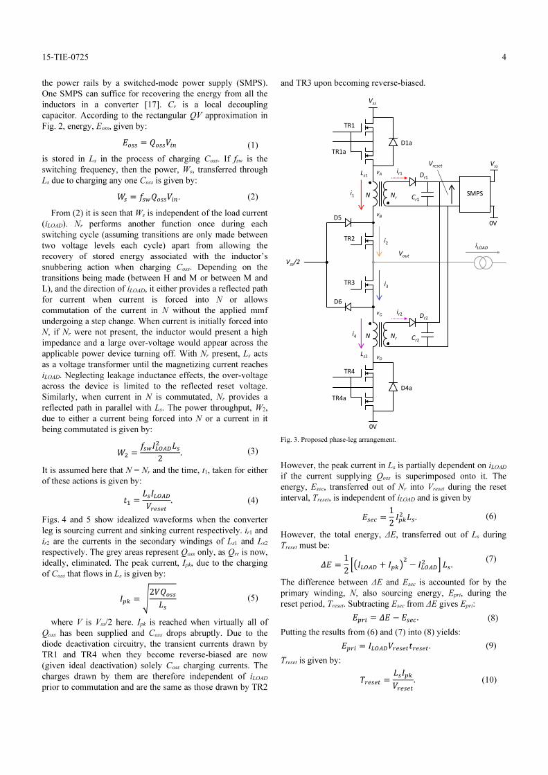
III. PROPOSED ARRANGEMENT
An objective is to identify the minimum ancillary circuit
requirements based on the switching actions listed in Tables 1
and 2, where linear inductors are used to control charging of
Coss. Fig. 3 shows the proposed arrangement [25]. As TR1 and
TR4 are subjected to intrinsic diode recovery effects, the local
intrinsic diode deactivation circuits in [16] are included. By
inspecting the far right-hand columns in Tables 1 and 2 it is
seen that both TR2 and TR3 lie in all the charging current
routes. Locating one snubber inductor directly in series with
either TR2 or TR3 should therefore suffice to control the Coss

15-TIE-0725
3
charging currents into all four MOSFETs.
Fig. 1. Three-level NPC converter phase-leg based around MOSFETs.
Fig. 2. Rectangular approximation of QV characteristic of output capacitance of super-junction MOSFET.
However, a difficulty arises with inductor reset. Consider,
for example, where the transition from Stage 6 to Stage 7 in
Table 1 is made. TR4 effectively turns off when it has drawn
most of its Qoss and its Coss then falls rapidly.
TABLE 1. OPERATION OF POWER DEVICES WITH CURRENT FLOWING OUT OF BRIDGE-LEG
Stage Output
voltage
level
Gate-drive signals (1 = on, 0 = off)
States of power devices
• Fwd = conducting in forward direction
• Rev = intrinsic diode conducting
• SR = acting as synchronous rectifier and conducting in reverse direction
• 0 = not conducting
Devices drawing
diode recovery
charge, Qrr, or Coss
charge, Qoss, when
transition into stage
is made
Charging
current
routes
TR1 TR2 TR3 TR4 TR1 TR2 TR3 TR4 D5 D6
1 H 1 1 0 0 fwd fwd 0 0 0 0 D5 (Qrr), TR3 (Qoss) TR1, 2, 3**
2 M 0 1 0 0 0 fwd 0 0 fwd 0 none none
3 M 0 1 1 0 0 fwd 0 0 fwd 0 none none
4 L 0 0 1 0 0 0 SR rev 0 0 none none
5 L 0 0 1 1 0 0 SR SR 0 0 none none
6 L 0 0 1 0 0 0 SR rev 0 0 none none
7 M 0 1 1 0 0 fwd 0 0 fwd 0 TR4 (Qrr + Qoss) D5, TR2, 3, 4
8* M 0 1 0 0 0 fwd 0 0 fwd 0 none none
*The circuit then transitions back to Stage 1. **The reverse recovery current drawn by D5 is neglected here.
TABLE 2. OPERATION OF POWER DEVICES WITH CURRENT FLOWING INTO BRIDGE-LEG
Stage Output
voltage
level
Gate-drive signals (1 = on, 0 = off)
States of power devices
• Fwd = conducting in forward direction
• Rev = intrinsic diode conducting
• SR = acting as synchronous rectifier and conducting in reverse direction
• 0 = not conducting
Devices drawing
diode recovery
charge, Qrr, or Coss
charge, Qoss, when
transition into stage
is made
Charging
current
routes
TR1 TR2 TR3 TR4 TR1 TR2 TR3 TR4 D5 D6
1 H 1 1 0 0 SR SR 0 0 0 0 none none
2 H 0 1 0 0 rev SR 0 0 0 0 none none
3 M 0 1 1 0 0 0 fwd 0 0 fwd TR1 (Qrr + Qoss) D6, TR1, 2, 3
4 M 0 0 1 0 0 0 fwd 0 0 fwd none none
5 L 0 0 1 1 0 0 fwd fwd 0 0 D6 (Qrr), TR2 (Qoss) TR2, 3, 4**
6 M 0 0 1 0 0 0 fwd 0 0 fwd none none
7 M 0 1 1 0 0 0 fwd 0 0 fwd none none
8* H 0 1 0 0 rev SR 0 0 0 0 none none
*The circuit then transitions back to Stage 1. **The reverse recovery current drawn by D6 is neglected here.
Energy has been stored in the inductor and it is now
necessary to reset it but, in Stage 7, TR2, TR3, D6 and D5
would form a zero-volt loop around N, thereby preventing
effective resetting. For this reason, the circuit with two
inductors in Fig. 3 is used as either TR1 or TR4 lie in all the
charging routes. Inductor reset is implemented by a secondary
winding, Nr, on each inductor that transfers energy into a
voltage sink, Vreset, via a diode, Dr. This energy is returned to
Vss
D1
D2
D3
D4
Vss/2
0V
D5
D6
iout
TR1
TR2
TR3
TR4
0V
TR1 D1
Coss
L
vc
v
Qoss
Q
ioss
vc
15-TIE-0725
4
the power rails by a switched-mode power supply (SMPS).
One SMPS can suffice for recovering the energy from all the
inductors in a converter [17]. Cr is a local decoupling
capacitor. According to the rectangular QV approximation in
Fig. 2, energy, Eoss, given by:
= (1)
is stored in Ls in the process of charging Coss. If fsw is the
switching frequency, then the power, Ws, transferred through
Ls due to charging any one Coss is given by:
= . (2)
From (2) it is seen that Ws is independent of the load current
(iLOAD). Nr performs another function once during each
switching cycle (assuming transitions are only made between
two voltage levels each cycle) apart from allowing the
recovery of stored energy associated with the inductor’s
snubbering action when charging Coss. Depending on the
transitions being made (between H and M or between M and
L), and the direction of iLOAD, it either provides a reflected path
for current when current is forced into N or allows
commutation of the current in N without the applied mmf
undergoing a step change. When current is initially forced into
N, if Nr were not present, the inductor would present a high
impedance and a large over-voltage would appear across the
applicable power device turning off. With Nr present, Ls acts
as a voltage transformer until the magnetizing current reaches
iLOAD. Neglecting leakage inductance effects, the over-voltage
across the device is limited to the reflected reset voltage.
Similarly, when current in N is commutated, Nr provides a
reflected path in parallel with Ls. The power throughput, W2,
due to either a current being forced into N or a current in it
being commutated is given by:
=
2. (3)
It is assumed here that N = Nr and the time, t1, taken for either
of these actions is given by:
= . (4)
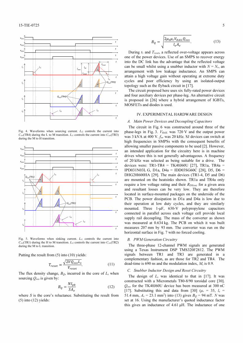
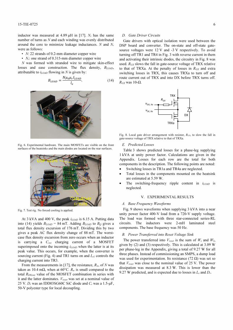
Figs. 4 and 5 show idealized waveforms when the converter
leg is sourcing current and sinking current respectively. ir1 and
ir2 are the currents in the secondary windings of Ls1 and Ls2
respectively. The grey areas represent Qoss only, as Qrr is now,
ideally, eliminated. The peak current, Ipk, due to the charging
of Coss that flows in Ls is given by:
= 2 (5)
where V is Vss/2 here. Ipk is reached when virtually all of
Qoss has been supplied and Coss drops abruptly. Due to the
diode deactivation circuitry, the transient currents drawn by
TR1 and TR4 when they become reverse-biased are now
(given ideal deactivation) solely Coss charging currents. The
charges drawn by them are therefore independent of iLOAD
prior to commutation and are the same as those drawn by TR2
and TR3 upon becoming reverse-biased.
Fig. 3. Proposed phase-leg arrangement.
However, the peak current in Ls is partially dependent on iLOAD
if the current supplying Qoss is superimposed onto it. The
energy, Esec, transferred out of Nr into Vreset during the reset
interval, Treset, is independent of iLOAD and is given by
=1
2 . (6)
However, the total energy, ∆E, transferred out of Ls during
Treset must be:
=1
2 + − . (7)
The difference between ∆E and Esec is accounted for by the
primary winding, N, also sourcing energy, Epri, during the
reset period, Treset. Subtracting Esec from ∆E gives Epri:
= − . (8)
Putting the results from (6) and (7) into (8) yields:
= . (9)
Treset is given by:
= . (10)
Vss
Vss/2
0V
D5
D6
D1a
TR1
TR2
TR1a
TR3
TR4
D4a
TR4a
i2
i3
Ls1
Ls2
iLOAD
N Nr
SMPS
Dr1
Cr1
Vreset
0V
N Nr
Dr2
Cr2
i1
i4
ir1
ir2
Vss
Vout
vA
vB
vC
vD
15-TIE-0725
5
Fig. 4. Waveforms when sourcing current. Ls2 controls the current into Coss(TR4) during the L to M transition. Ls1 controls the current into Coss(TR3) during the M to H transition.
Fig. 5. Waveforms when sinking current. Ls1 controls the current into Coss(TR1) during the H to M transition. Ls2 controls the current into Coss(TR2) during the M to L transition.
Putting the result from (5) into (10) yields:
= 2 . (11)
The flux density change, BQ, incurred in the core of Ls when
sourcing Qoss is given by:
=
(12)
where S is the core’s reluctance. Substituting the result from
(5) into (12) yields:
= 2
. (13)
During t1 and Treset, a reflected over-voltage appears across
one of the power devices. Use of an SMPS to recover energy
into the DC link has the advantage that the reflected voltage
can be small whilst using a snubber inductor with N = Nr, an
arrangement with low leakage inductance. An SMPS can
attain a high voltage gain without operating at extreme duty
cycles and poor efficiency by using an isolated-output
topology such as the flyback circuit in [17].
The circuit proposed here uses six fully-rated power devices
and four auxiliary devices per phase-leg. An alternative circuit
is proposed in [26] where a hybrid arrangement of IGBTs,
MOSFETs and diodes is used.
IV. EXPERIMENTAL HARDWARE DESIGN
A. Main Power Devices and Decoupling Capacitors
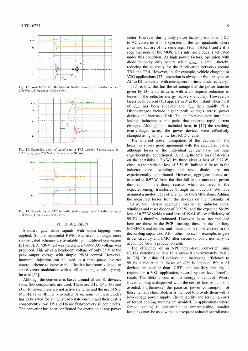
The circuit in Fig. 6 was constructed around three of the
phase-legs in Fig. 3. VRAIL was 720 V and the output power
was 3 kVA at 400 V. fsw was 20 kHz. SJ devices can switch at
high frequencies in SMPSs with the consequent benefits of
allowing smaller passive components to be used [2]. However,
an intended application for the circuitry here is in machine
drives where this is not generally advantageous. A frequency
of 20 kHz was selected as being suitable for a drive. The
devices were: TR1-TR4 = TK40J60U [27], TR1a, TR4a =
IPD031N03L G, D1a, D4a = IDD03SG60C [28], D5, D6 =
DHG20I600HA [29]. The main devices (TR1-4, D5 and D6)
are mounted on the heatsinks shown. TR1a and TR4a only
require a low voltage rating and their RDS(on) for a given area
and resultant losses can be very low. They are therefore
located in surface-mounted packages on the underside of the
PCB. The power dissipation in D1a and D4a is low due to
their operation at low duty cycles, and they are similarly
mounted. Three 1-µF, 630-V polypropylene capacitors
connected in parallel across each voltage cell provide local
supply rail decoupling. The mass of the converter as shown
was measured at 0.634 kg. The PCB on which it was built
measures 207 mm by 93 mm. The converter was run on the
horizontal surface in Fig. 7 with no forced cooling.
B. PWM Generation Circuitry
The three-phase 12-channel PWM signals are generated
using a Texas Instrument DSP TMS320F2812. The PWM
signals between TR1 and TR3 are generated in a
complementary fashion, as are those for TR2 and TR4. The
dead-time is 690 ns and the modulation index, M, is 0.9.
C. Snubber Inductor Design and Reset Circuitry
The design of Ls was identical to that in [17]. It was
constructed with a Micrometals T80-8/90 toroidal core [30].
Qoss for the TK40J60U device has been measured at 300 nC
[17]. Substituting this and data from [30] (µr = 35, le =
51.4 mm, Ae = 23.1 mm2) into (13) gives BQ = 94 mT. N was
set at 16. Using the manufacturer’s quoted inductance factor
this gives an inductance of 4.61 µH. The inductance of one
vGS1
vGS2
i2
i3
t
t
t
t
t
t
vGS3
vGS4
Qoss(TR4)
Qoss(TR3)
i1
t
i4
t
ir1
ir1
ir2ir2
ILOAD
IpkImax
treset
i2
i3
t
t
Qoss(TR2)
vGS1
vGS2
t
t
t
t
vGS3
vGS4
i1
t
Qoss(TR1)
i4
t
ir2
ir2
ir1 i
r1
15-TIE-0725
6
inductor was measured at 4.89 µH in [17]. Nr has the same
number of turns as N and each winding was evenly distributed
around the core to minimize leakage inductances. N and Nr
were as follows:
• N: 22 strands of 0.2-mm diameter copper wire
• Nr: one strand of 0.315-mm diameter copper wire
N was formed with stranded wire to mitigate skin-effect
losses and ease construction. The flux density, BLOAD,
attributable to iLOAD flowing in N is given by:
. (14)
Fig. 6. Experimental hardware. The main MOSFETs are visible on the front
surfaces of the heatsinks and the main diodes are located on the rear surfaces.
Fig. 7. Test rig. No forced cooling is applied.
At 3 kVA and 400 V, the peak iLOAD is 6.15 A. Putting data
into (14) yields BLOAD = 84 mT. Adding BLOAD to BQ gives a
total flux density excursion of 176 mT. Dividing this by two
gives a peak AC flux density change of 88 mT. The worst-
case flux density excursion from zero occurs when an inductor
is carrying a Coss charging current of a MOSFET
superimposed onto the incoming iLOAD when the latter is at its
peak value. This occurs, for example, when the converter is
sourcing current (Fig. 4) and TR1 turns on and Ls1 controls the
charging current into TR3.
From the measurements in [17], the resistance, Rw, of N was
taken as 10.4 mΩ, when at 60°C. Rw is small compared to the
total RDS(on) value of the MOSFET combination in series with
it and the latter dominates. Vreset was set at a nominal value of
25 V. Dr was an IDD03SG60C SiC diode and Cr was a 1.5-µF,
50-V polyester type for local decoupling.
D. Gate Driver Circuits
Gate drivers with optical isolation were used between the
DSP board and converter. The on-state and off-state gate-
source voltages were 12 V and -3 V respectively. To avoid
turning off TR1 and TR4 in Fig. 3 with reverse current in them
and activating their intrinsic diodes, the circuitry in Fig. 8 was
used. RGX slows the fall in gate-source voltage of TRX relative
to that of TRXa. At the penalty of losses in RGX and extra
switching losses in TRX, this causes TRXa to turn off and
route current out of TRX and into DX before TRX turns off.
RGX was 10-Ω.
Fig. 8. Local gate driver arrangement with resistor, RGX, to slow the fall in
gate-source voltage of TRX relative to that of TRXa.
E. Predicted Losses
Table 3 shows predicted losses for a phase-leg supplying
1 kVA at unity power factor. Calculations are given in the
Appendix. Losses for each row are the total for both
components in the description. The following points are noted:
• Switching losses in TR1a and TR4a are neglected.
• Total losses in the components mounted on the heatsink
are estimated at 5.59 W.
• The switching-frequency ripple content in iLOAD is
neglected.
V. EXPERIMENTAL RESULTS
A. Base Frequency Waveforms
Fig. 9 shows waveforms when supplying 3 kVA into a near
unity power factor 400-V load from a 720-V supply voltage.
The load was formed with three star-connected series-RL
circuits. The inductors were 2-mH laminated steel
components. The base frequency was 50 Hz.
B. Power Transferred into Reset Voltage Sink
The power transferred into Vreset is the sum of Ws and W2,
given by (2) and (3) respectively. This is calculated at 3.09 W
per phase-leg in the Appendix, giving a total of 9.27 W for all
three phases. Instead of commissioning an SMPS, a dump load
was used for experimentation. Its resistance (72 Ω) was set so
that Vreset was close to the nominal value of 25 V. The power
dissipation was measured at 8.3 W. This is lower than the
9.27 W predicted, and is expected due to losses in Ls and Dr.
TRX
vGX, Xa
DX
vSX, Xa
TRXa
RGX
15-TIE-0725
7
TABLE 3. PREDICTED LOSSES FROM ONE PHASE-LEG
Description Loss
(W)
Applicable
section in
Appendix
Loss in
components
in bridge-leg
Phase-leg
components
mounted on
heatsink
Conduction loss in TR1
and TR4
1.11 A.
Switching loss in main
switches (TR1 and TR4)
1.02 B.
Switching loss in main
switches (TR2 and TR3)
0
Self-discharge loss in
TR1 and TR4
0.32 C.
Conduction loss in inner
switches (TR2 and TR3)
1.51 D.
Conduction loss in D5
and D6
1.63 E.
Phase-leg
components
mounted on
pcb
Conduction loss in TR1a
and TR4a
0.06 F.
Dead-time loss in D1a
and D4a
0.14 G.
Snubber
inductors
Conduction loss (Ls1 and
Ls2)
0.15 H.
Core loss (Ls1 and Ls2) 0.50 I.
Losses in reset circuitry
Reset diode (Dr1 and Dr2)
loss
0.16 J.
Losses in SMPS 0.77 K.
Total estimated loss 7.37
Fig. 9. Base-frequency waveforms showing an output voltage from one phase
and the three output currents. The top trace is the voltage. Scales: vout =
500 V/div, iLOAD = 5 A/div. Time scale = 5 ms/div.
C. Thermal Measurements
Fig. 10 shows a thermal photograph of the circuit running at
full load, as in Fig. 9, and in the hard thermal steady-state.
Before proceeding with the thermal tests, one of the heatsinks
was thermally characterized. A DC current was passed
through the path from the source of TR3 to the drain of TR2
and the voltage developed was measured. The thermal
resistance was estimated at 4.74°C/W by recording the
heatsink’s temperature rise above ambient. The total loss of
the components mounted on the heatsinks was estimated at
17.3 W from the average temperature rises of the heatsinks.
Due to the proximity of the heatsinks to each other, and the
heating effect of losses incurred from circuitry not mounted on
the heatsinks, this is expected to be an overestimate. Although
the central heatsink is at a higher temperature than the other
two, this is only by approximately 2°C and is expected given
its physical location.
Fig. 10. Thermal photograph of the circuit in Figs. 6 and 7 when supplying
3 kVA into a unity power factor load and in the hard thermal steady-state.
D. Exemplifying Switching-Frequency Waveforms with Current out of Converter and Positive Output Voltage
Fig. 11 shows switching-frequency waveforms from a
phase-leg running under steady-state DC conditions and
switching between the “H” and “M” voltage levels so that it
outputs a positive voltage. The duty cycle was set so that the
average output voltage, vout, is 230 V. An RL load is
connected between vout and Vss/2. For this test an inductor of
3.9 mH based around ferrite cores was used. iLOAD is 4.35 A.
This corresponds to those instances in the AC cycle in Fig. 9
where ωt = 0.785 rads and 2.356 rads. The quantities shown
are: iLOAD, the current (i1) in the primary winding of Ls1, the
drain voltage of TR1a (vA) and the drain voltage of TR2 (vB).
For practical purposes vA is very close to the source voltage of
TR1. An overshoot voltage (circle “A”) is seen at vA when
current is forced out of Ls1 at TR1 turn-off. An overshoot
voltage (circle “B”) is seen at vB at Ls1 reset. iLOAD was
measured with a high-bandwidth DC current probe. i1 was
measured with a sensor based on a Rogowski coil as this
introduces less physical disruption and consequent stray
inductance in series with N. The resistance of the dump load
substituted for the SMPS was set to give a Vreset value close to
25 V. 227 Ω gave Vreset = 25.6 V. The power transferred into
the resistance was thus calculated at 2.89 W. Figs. 12 and 13
show waveforms at TR1 turn-on. Although no intrinsic diode
recovery action is taking place, a Coss charging current is
sourced into TR3. It is seen, Fig. 12, that the duration of Treset
is in good agreement with the value of 1.30 µs calculated with
(10). Fig. 14 shows waveforms at TR1 turn off where it is also
seen that t1 is in good agreement with the value of 0.85 µs
calculated with (4).
Fig. 11. Switching-frequency waveforms showing complete switching cycles.
Scales: iLOAD, i1 = 5 A/div, vA, vB = 200 V/div, Time scale = 20 µs/div.

15-TIE-0725
8
Fig. 12. Waveforms at TR1 turn-on. Scales: iLOAD, i1 = 5 A/div, vA, vB =
200 V/div, Time scale = 500 ns/div.
Fig. 13. Expanded view of waveforms at TR1 turn-on. Scales: iLOAD, i1 =
5 A/div, vA, vB = 200 V/div, Time scale = 200 ns/div.
Fig. 14. Waveforms at TR1 turn-off. Scales: iLOAD, i1 = 5 A/div, vA, vB =
200 V/div, Time scale = 500 ns/div.
E. Exemplifying Switching-Frequency Waveforms with Current out of Converter and Negative Output Voltage
For these tests the RL load was connected between the vout
terminal of a phase-leg and 0V, Fig. 15. Although this is not a
standard configuration and the power flow is from the DC
supply, an outer device is forced to act as a freewheeling
device as is the case with AC to DC (rectifier) operation. In
this case the behavior of its intrinsic diode has to be addressed
in conjunction with the charging of its Coss, as is the case with
the L to M and H to M transitions in Tables 1 and 2
respectively. The switching stresses are thus those
encountered with operation as an AC to DC converter. The
switching duty factor was set so that the load voltage (not
output voltage) is 230 V with an average iLOAD of 4.35 A.
Fig. 15. Connection arrangement with positive output current and negative
output voltage (when referenced to mid-point, Vss/2). The ancillary circuitry is
not shown for clarity.
Fig. 16 shows exemplifying switching-frequency
waveforms from one of the phase-legs. As in Section D, the
phase-leg is running under steady-state DC conditions. In this
case it transitions between the “M” and “L” voltage levels to
output a negative voltage. Four quantities are shown: iLOAD, the
current (i4) in the primary winding of Ls2, the source voltage of
TR3 (vC) and the drain voltage of TR4 (vD). iLOAD was, again,
measured using a high-bandwidth DC current probe. As with
i1, i4 was measured using a sensor based around a Rogowski
coil. Vreset was measured at 24.52 V. Given the dump
resistance value of 227 Ω used here, the power transferred into
the resistance was calculated at 2.65 W.
Fig. 16. Switching-frequency waveforms showing complete switching cycles.
Scales: iLOAD, i4 = 5 A/div, vC, vD = 200 V/div, Time scale = 20 µs/div.
Figs. 17 and 18 show waveforms at TR2 turn-on. Fig. 19
shows waveforms at TR2 turn-off. The power transferred into
Vreset is similar for the two situations where firstly a
capacitance has to be charged (2.89 W) and secondly both a
Coss has to be charged and an intrinsic diode has to be
deactivated (2.65 W). Also, the observed Qoss is approximately
300 nC in both cases. Qoss is taken from the current-time
overshoot products in i1 and i4 in Figs. 13 and 17 respectively.
It is therefore inferred that intrinsic diode deactivation is
effective.
Vss
D1
D2
D3
D4
Vss/2
0V
D5
D6
iout
TR1
TR2
TR3
TR4
Lout
RLOAD
vload
15-TIE-0725
9
Fig. 17. Waveforms at TR2 turn-on. Scales: iLOAD, i4 = 5 A/div, vC, vD =
200 V/div, Time scale = 500 ns/div.
Fig. 18. Expanded view of waveforms at TR2 turn-on. Scales: iLOAD, i4 =
5 A/div, vC, vD = 200 V/div, Time scale = 200 ns/div.
Fig. 19. Waveforms at TR2 turn-off. Scales: iLOAD, i4 = 5 A/div, vC, vD =
200 V/div, Time scale = 500 ns/div.
VI. DISCUSSION
Standard gate drive signals with under-lapping were
applied. Simple sinusoidal PWM was used, although more
sophisticated schemes are available for multilevel conversion
[31]-[36]. A 720-V rail was used and a 400-V AC voltage was
produced. This gives a headroom voltage of only 35 V at the
peak output voltage with simple PWM control. However,
harmonic injection can be used in a three-phase inverter
control scheme to increase the effective headroom voltage, or
space vector modulation with a cell-balancing capability may
be used [33].
Although the converter is based around silicon SJ devices,
some SiC components are used. These are D1a, D4a, Dr1 and
Dr2. However, these are not active switches and the use of SiC
MOSFETs or JFETs is avoided. Also, none of these diodes
has to be rated for a high steady-state current and their cost is
consequently low. D5 and D6 are fast-recovery silicon diodes.
The converter has been configured for operation at any power
factor. However, during unity power factor operation as a DC
to AC converter it only operates in the two quadrants where
iLOAD and vout are of the same sign. From Tables 1 and 2 it is
seen that none of the MOSFET’s intrinsic diodes is activated
under this condition. At high power factors, operation with
diode recovery only occurs when iLOAD is small, thereby
reducing the necessity for the deactivation networks around
TR1 and TR4. However, in, for example, vehicle charging or
V2G applications [37], operation is always or frequently as an
AC to DC converter with consequent intrinsic diode recovery.
If Ls is low, this has the advantage that the power transfer
given by (3) tends to zero, with a consequent reduction in
losses in the inductor energy recovery circuitry. However, a
larger peak current (Ipk) appears in N at the instant when most
of Qoss has been supplied and Coss then rapidly falls.
Disadvantages include higher peak voltages across power
devices and increased EMI. The snubber inductors introduce
leakage inductances into paths that undergo rapid current
changes. Although not included here, in [17] the resulting
over-voltages across the power devices were effectively
clamped using simple low-loss RCD circuits.
The inferred power dissipation of the devices on the
heatsinks shows good agreement with the calculated value,
although losses in the individual devices have not been
experimentally apportioned. Dividing the total loss of devices
on the heatsinks (17.3 W) by three gives a loss of 5.77 W,
close to the predicted loss of 5.59 W. Individual losses in the
inductor cores, windings and reset diodes are not
experimentally apportioned. However, aggregate losses are
inferred at 0.97 W from the shortfall in the measured power
dissipation in the dump resistor when compared to the
expected energy transferred through the inductors. We have
assumed a modest 75% efficiency for the SMPS stage. Adding
the measured losses from the devices on the heatsinks of
17.3 W, the inferred aggregate loss in the inductor cores,
windings and reset diodes of 0.97 W, and the expected SMPS
loss of 0.77 W yields a total loss of 19.04 W. An efficiency of
99.3% is therefore estimated. However, losses not included
here are those in the PCB tracking, those in the auxiliary
MOSFETs and diodes, and losses due to ripple current in the
decoupling capacitors. Also, other losses, for example, in gate
driver circuitry and EMC filter circuitry, would normally be
accounted for in a production unit.
The efficiency of an NPC three-level converter using
IGBTs switching at 20 kHz is given at approximately 98.8%
in [38]. By using SJ devices and increasing efficiency to
99.3% a reduction in losses of 42% is attained. Whilst SJ
devices are costlier than IGBTs and ancillary circuitry is
required in a VSC application, several system-level benefits
result. The lifetime cost in lost energy is reduced. Where
forced cooling is dispensed with, the cost of fans or pumps is
avoided. Furthermore, the parasitic power consumption of
these items is eliminated, as is the need to provide them with a
low-voltage power supply. The reliability and servicing costs
of forced cooling systems are avoided. In applications where
forced cooling is undesirable or impermissible, smaller
heatsinks may be used with a consequent reduced overall mass

15-TIE-0725
10
and bulk. This is particularly advantageous in aerospace power
systems. High efficiencies are also attainable with SiC
devices, but these are costlier than SJ devices and, in the case
of SiC MOSFETs, there are concerns over gate oxide behavior
[39].
VII. CONCLUSION
Silicon super-junction MOSFETs can be readily deployed
in a three-level neutral point clamped converter provided the
behavior of the intrinsic diodes in the outer devices and
charging of the output capacitances of all the MOSFETs is
addressed. 99.3% efficiency has been estimated in a naturally-
cooled converter operating from a 720-V DC rail, switching at
20 kHz, and supplying 3 kVA. Target applications are where
forced cooling is undesirable or not possible, and low losses
are consequently essential to reduce cooling requirements.
VIII. APPENDIX
Loss formulae for one phase-leg are given in this appendix.
Values are calculated for a 1-kVA unity power factor load.
A. Conduction Loss in Main Outer Switches (TR1 and TR4)
As iLOAD is 4.35 A, its peak value, Ip, is 6.15 A. vout is 230 V
(phase) and its peak phase value, Vp, is 325 V. The effective
input voltage for calculating duty cycles is half of 720 V, at
360 V. The total on-state loss in TR1 and TR4 is given by:
. (A1)
iLOAD(t) is given by:
sin (A2)
where φ is the phase angle of iLOAD. δ(t) is given by:
sin. (A3)
The modulation depth, M, is defined as:
. (A4)
Hence δ(t) may be expressed as:
sin. (A5)
The results from (A2) and (A5) are put into (A1) and Wave is
then derived as:
12
12 4 cos 2". (A6)
RDS(on) for TR1-4 is taken as 80 mΩ. This was estimated from
[26] as being the approximate value at a junction temperature
of 60°C. Putting values into (A6) gives a loss of 1.11 W.
B. Switching Loss in Main Switches (TR1-4)
Each switching cycle a power device is switching iLOAD on and
off. Which device switches depends on the direction of iLOAD
and whether the transitions are between H and M or between
M and L. The total loss is independent of φ and is given by:
# $%
. (A7)
where tr is the rise time and tf is the fall time. The total
switching loss in TR1 and TR4 is given by:
# $%2
1 cos. (A8)
The total switching loss in TR2 and TR3 is given by:
# $%2
1 cos . (A9)
tf and tr are each estimated at approximately 40 ns by
observation. Putting the values into (A8) and (A9) gives
1.02 W and 0 W respectively. Due to the self-snubbering
action of Coss, turn-off losses may be over-estimated.
C. Self-Discharge Loss in TR1 and TR4
The data in [27] gives Coss for vDS between 0.1 V and 100 V.
We have derived a QV curve from this data and linearly
extrapolated the curve to 360 V at the gradient (capacitance)
observed at 100 V. The stored energy is estimated at 16.1 µJ.
Multiplying this by the switching frequency of 20 kHz yields a
power dissipation due to self-discharge of 322 mW.
D. Conduction Loss in TR2 and TR3
This is calculated from:
. (A10)
Putting values into (A10) (RDS(on) = 80 mΩ) yields 1.51 W.
E. Conduction Loss in D5 and D6
This is calculated from:
#1 $. (A11)
Putting the results from (A2) and (A5) into (A11) yields:
&' 1 sin. (A12)
The average value derived from (A12) is:
2
4
4 2 cos 4 sin". (A13)
The diode forward voltage drop, Vf, is estimated at 1.3 V from
[29]. Putting this and other values into (A13) yields 1.63 W.
F. Conduction Loss in Auxiliary Switches (TR1a and TR4a)
This was calculated from (A6), but with the RDS(on) value for
the auxiliary MOSFETs entered. This was estimated at 4 mΩ
at a junction temperature of 60°C from the data in [28].
Putting the values at unity power factor into (A6) yields
0.06 W.
G. Dead-Time Loss in D1a and D4a
This is calculated from:
2(% (A14)
where Tdead is the dead-time. Averaging the integral of (A14)
between the appropriate limits yields:
4(%
. (A15)
Putting Tdead = 690 ns and Vf = 1.3 V into (A15) gives 0.14 W.
H. Conduction Loss (Ls1 and Ls2)
This is given by (A6), but with Rw substituted for RDS(on):

15-TIE-0725
11
=12 × 12 + 4 cos 2. (A16)
Putting the values into (A16) (Rw = 10.4 mΩ) yields 0.15 W.
I. Core Loss (Ls1 and Ls2)
The loss density for the -8 material was estimated at
416 mW/cm3 from the curve-fit formula in [30]. This was then
multiplied by the effective volume of the T80-8/90 core
(1.19 cm3) to yield a loss of 495 mW. The peak AC flux
density excursion entered was 88 mT, that is, the value when
iLOAD is at its peak level. The frequency entered was 20 kHz.
However, this is only the frequency of the fundamental
component of the flux density excursion and there is a high
harmonic content. On the other hand, the peak iLOAD was used.
J. Reset Diode (Dr) Loss
Before calculating reset circuit losses, the energy
transferred out of Nr is calculated. Putting the data into (2)
gives 2.16 W. The power transferred through Ls due to forcing
iLOAD into it or commutating iLOAD is given by (3). Where iLOAD
varies sinusoidally, the average power transfer is given by:
=2 !"#$%#
. (A17)
Putting the data into (A17) gives 925 mW. Adding the
results from (2) and (A17) gives 3.09 W. If this is transferred
into Vreset, then the average current through Dr into a 25-V
reset voltage is 124 mA. If Dr’s forward voltage drop is taken
as 1.3 V, this gives a loss of 161 mW. Losses in Ls are
neglected in estimating the power transferred through Dr.
K. Losses in SMPS
A modest 75% efficiency is assumed for the SMPS. This
gives a loss of 773 mW with an input power of 3.09 W. Losses
in Ls and Dr are neglected in estimating the power transferred
into the SMPS.
REFERENCES
[1] J.-S. Lai, B.-M. Song, R. Zhou, A. Hefner, Jr., D. W. Berning, and C.-C. Shen, “Characteristics and utilization of a new class of low on-resistance MOS-gated power device”, IEEE Transactions on Industry Applications, Vol. 37, No. 5, pp. 1282-1289, September/October 2001.
[2] L. Lorenz, G. Deboy, and I. Zverev, “Matched pair of Coolmos transistor with SiC-schottky diode - advantages in application”, IEEE Transactions on Industry Applications, Vol. 40, No. 5, pp. 1265-1272, September/October 2004.
[3] R. A. Wood and T. E. Salem, “Evaluation of a 1200-V, 800-A all-SiC dual module”, IEEE Transactions on Power Electronics, Vol. 26, No. 9, pp. 2504-2511, September 2011.
[4] M. M. Farag, S. M. Gadoue, A. L. Mohamadein, A. M. Massoud, and S. Ahmed, “Elimination of reverse recovery effects associated with Coolmos devices employing current source inverter topology”, Proceedings, 6th IET Power Electronics, Machines and Drives Conference (PEMD 2012), Bristol, UK, March 2012.
[5] J. Biela, J. W. Kolar, and G. Deboy, “Optimal design of a compact 99.3% efficient single-phase PFC rectifier”, Proceedings, 25th Annual Applied Power Electronics Conference and Exposition (APEC’10), Palm Springs, CA, pp. 1397-1404, February 2010.
[6] J. W. Kolar and T. Friedli, “The essence of three-phase PFC rectifier systems—part I”, IEEE Transactions on Power Electronics, Vol. 28, No. 1, pp. 176-198, January 2013.
[7] T. Friedli, M. Hartmann, and J. W. Kolar, “The essence of three-phase PFC rectifier systems—part II”, IEEE Transactions on Power Electronics, Vol. 29, No. 2, pp. 543-560, February 2014.
[8] S. V. Araújo, P. Zacharias, and R. Mallwitz, “Highly efficient single-phase transformerless inverters for grid-connected photovoltaic systems”, IEEE Transactions on Industrial Electronics, Vol. 57, No. 9, pp. 3118-3128, September 2010.
[9] P. Sun, C. Liu, J.-S. Lai, C.-L. Chen, and N. Kees, “Three-phase dual-buck inverter with unified pulsewidth modulation”, IEEE Transactions on Power Electronics, Vol. 27, No. 3, pp. 1159-1167, March 2012.
[10] W. Yu, H. Qian, and J.-S. Lai, “Design of high-efficiency bidirectional DC-DC converter and high-precision efficiency measurement”, Proceedings, 34th Annual IEEE Industrial Electronics Conference (IECON 2008), Orlando, FL, pp. 685-690, November 2008.
[11] C. Marxgut, F. Krismer, D. Bortis, and J. W. Kolar, “Ultraflat interleaved triangular current mode (TCM) single-phase PFC rectifier”, IEEE Transactions on Power Electronics, Vol. 29, No. 2, pp. 873-882, February 2014.
[12] J. Zhang and J.-S. Lai, “A synchronous rectification featured soft-switching inverter using CoolMOS”, Proceedings, 21st Annual IEEE Applied Power Electronics Conference and Exposition (APEC’06), Dallas, TX, USA, pp. 810-815, March 2006.
[13] P. Sun, J.-S. Lai, H. Qian, W. Yu, C. Smith, and J. Bates, “High efficiency three-phase soft-switching inverter for electric vehicle drives”, Proceedings, 5th IEEE Vehicle Power and Propulsion Conference (VPPC '09), Dearborn, MI, USA, pp. 761-766, September 2009.
[14] P. Anthony and N. McNeill, “The efficient deployment of silicon super-junction MOSFETs as synchronous rectifiers”, Proceedings, 7th IET Power Electronics, Machines and Drives Conference (PEMD 2014), Manchester, UK, April 2014.
[15] R. M. Martinelli, “Synchronous rectifier bi-directional converter”, Patent Application No. EP2461472 (A2), 6 June 2012.
[16] D. B. DeWitt, C. D. Brown, and S. M. Robertson, “System and method for reducing body diode conduction”, US Patent No. 7508175 (B2), 24 March 2009.
[17] N. McNeill, P. Anthony, and N. Oswald, “Ultra-high efficiency machine drive inverter using super-junction MOSFETs”, Proceedings, 7th IET Power Electronics, Machines and Drives Conference (PEMD 2014), Manchester, UK, April 2014.
[18] G. Grandi, J. Loncarski, and O. Dordevic, “Analysis and comparison of peak-to-peak current ripple in two-level and multilevel PWM inverters”, IEEE Transactions on Industrial Electronics, Vol. 62, No. 5, pp. 2721-2730, May 2015.
[19] J. Rodríguez, J.-S. Lai, and F. Z. Peng, “Multilevel inverters: a survey of topologies, controls, and applications”, IEEE Transactions on Industrial Electronics, Vol. 49, No. 4, pp. 724-738, August 2002.
[20] S. Kouro, M. Malinowski, K. Gopakumar, J. Pou, L. G. Franquelo, B. Wu, J. Rodriguez, M. A. Pérez, and J. I. Leon, “Recent advances and industrial applications of multilevel converters”, IEEE Transactions on Industrial Electronics, Vol. 57, No. 8, pp. 2553-2580, August 2010.
[21] T. Brückner and S. Bernet, “Loss balancing in three-level voltage source inverters applying active NPC switches”, Proceedings, 32nd Annual Power Electronics Specialists Conference (PESC 2001), Vancouver, Canada, Vol. 2, pp. 1135-1140, June 2001.
[22] T. Brückner, S. Bernet, and H. Güldner, “The active NPC inverter and its loss-balancing control”, IEEE Transactions on Industrial Electronics, Vol. 54, No. 6, pp. 855-868, June 2005.
[23] J. Li, A. Q. Huang, Z. Liang, and S. Bhattacharya, “Analysis and design of active NPC (ANPC) inverters for fault-tolerant operation of high-power electrical drives”, IEEE Transactions on Power Electronics, Vol. 27, No. 2, pp. 519-533, February 2012.
[24] N. Yamashita, N. Murakami, and T. Yachi, “Conduction power loss in MOSFET synchronous rectifier with parallel-connected Schottky barrier diode”, IEEE Transactions on Power Electronics, Vol. 13, No. 4, pp. 667-673, July 1998.
[25] N. McNeill, X. Yuan, and P. Anthony, “High-efficiency multilevel converter technology for electric vehicle applications using super-junction MOSFETs”, Proceedings, 5th IET Hybrid and Electric Vehicles Conference (HEVC 2014), London, UK, November 2014.
[26] Y. Wang and R. Li, “Novel high-efficiency three-level stacked-neutral-point-clamped grid-tied inverter”, IEEE Transactions on Industrial Electronics, Vol. 60, No. 9, pp. 3766-3774, September 2013.
[27] TK40J60U datasheet [Online], available: www.toshiba-components.com, accessed March 2013.

15-TIE-0725
12
[28] IPD031N03L G and IDD03SG60C datasheets [Online], available: www.infineon.com, accessed March 2013.
[29] DHG20I600HA datasheet [Online], available: www.ixys.com, accessed
March 2013.
[30] T80-8/90 and -8 Material datasheets [Online], available:
www.micrometals.com, accessed April 2013.
[31] P. Zanchetta, D. B. Gerry, V. G. Monopoli, J. C. Clare, and P. W.
Wheeler, “Predictive current control for multilevel active rectifiers with
reduced switching frequency”, IEEE Transactions on Industrial
Electronics, Vol. 55, No. 1, pp. 163-172, January 2008.
[32] F. H. Khan, L. M. Tolbert, and W. E. Webb, “Hybrid electric vehicle
power management solutions based on isolated and nonisolated
configurations of multilevel modular capacitor-clamped converter”,
IEEE Transactions on Industrial Electronics, Vol. 56, No. 8, pp. 3079-
3095, August 2009.
[33] C. Xia, H. Shao, Y. Zhang, and X. He, “Adjustable proportional hybrid SVPWM strategy for neutral-point-clamped three-level inverters, IEEE
Transactions on Industrial Electronics, Vol. 60, No. 10, pp. 4234-4242,
October 2013.
[34] J. I. Leon, S. Vazquez, R. Portillo, L. G. Franquelo, J. M. Carrasco, P.
W. Wheeler, and A. J. Watson, “Three-dimensional feedforward space
vector modulation applied to multilevel diode-clamped converters”,
IEEE Transactions on Industrial Electronics, Vol. 56, No. 1, pp. 101-
109, January 2009.
[35] R. Davoodnezhad, D. G. Holmes, and B. P. McGrath, “A novel three-
level hysteresis current regulation strategy for three-phase three-level
inverters”, IEEE Transactions on Power Electronics, Vol. 29, No. 11,
pp. 6100-6109, November 2014.
[36] B. Jacob and M. R. Baiju, “A new space vector modulation scheme for
multilevel inverters which directly vector quantize the reference space
vector”, IEEE Transactions on Industrial Electronics, Vol. 62, No. 1,
pp. 88-95, January 2015.
[37] M. Kesler, M. C. Kisacikoglu, and L. M. Tolbert, “Vehicle-to-grid
reactive power operation using plug-in electric vehicle bidirectional
offboard charger”, IEEE Transactions on Industrial Electronics, Vol. 61,
No. 12, pp. 6778-6784, December 2014.
[38] M. Schweizer and J. W. Kolar, “Design and implementation of a highly
efficient three-level T-type converter”, IEEE Transactions on Power
Electronics, Vol. 28, No. 2, pp. 899-907, February 2013.
[39] R. Ouaida, M. Berthou, J. León, X. Perpiñà, S. Oge, P. Brosselard, and
C. Joubert, “Gate oxide degradation of SiC MOSFET in switching
conditions”, IEEE Electron Device Letters, Vol. 35, No. 12, pp. 1284-
1286, December 2014.
Neville McNeill received the M.Phil. and
Ph.D. degrees in power electronics from
Napier University, Edinburgh, U.K., in
2003 and 2008 respectively.
His career has included periods
working for electric vehicle and
renewable energy companies. In 2004 he
became a research engineer in the
Electrical Energy Management Group
(EEMG), Department of Electrical and Electronic
Engineering, University of Bristol, Bristol, UK, where he is
now Senior Lecturer in Power Electronics. His present
research interests are in the area of high-efficiency multi-
kilowatt power electronic conversion for aerospace, renewable
energy and electric vehicle applications.
Dr McNeill is a member of the Institution of Engineering
and Technology, a Chartered Engineer with the Engineering
Council of the U.K. and a fellow of the Higher Education
Academy.
Xibo Yuan (S’09-M’11) received the
B.S. degree from China University of
Mining and Technology, Xuzhou, China
and the Ph.D degree from Tsinghua
University, Beijing, China, in 2005 and
2010, respectively, both in electrical
engineering.
He is currently a Senior Lecturer in the
Electrical Energy Management Group
(EEMG), Department of Electrical and Electronic
Engineering, the University of Bristol, Bristol, UK, where he
was a Lecturer from 2011 to July 2015. From 2007 to 2008, he
was a visiting scholar in Center for Power Electronics Systems
(CPES), Virginia Polytechnic Institute and State University,
Blacksburg, Virginia, USA. In early 2013, he was a visiting
scholar in the Institute of Energy Technology, Aalborg
University, Denmark. During 2010 and 2011, he was a post-
doctoral research associate in the Electrical Machines and
Drives (EMD) Research Group, Department of Electronic and
Electrical Engineering, the University of Sheffield, Sheffield,
UK. His research area include power electronics, wind power
generation, multilevel converters, sensor-less drive of
induction motor and permanent magnet motor, drive train
design for electric vehicles and more electric aircraft
technologies.
Dr Yuan is an Associate Editor of IET Power Electronics
and an International Scientific Committee Member of
European Power Electronics and Drives Association.
Philip Anthony, photograph and biography not available
at the time of publication.