Embed Size (px)
Citation preview
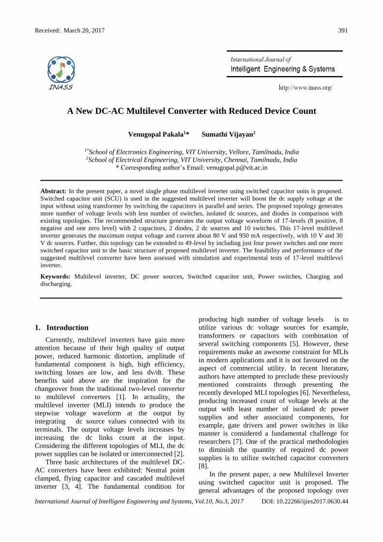
Received: March 20, 2017 391
International Journal of Intelligent Engineering and Systems, Vol.10, No.3, 2017 DOI: 10.22266/ijies2017.0630.44
A New DC-AC Multilevel Converter with Reduced Device Count
Venugopal Pakala1* Sumathi Vijayan2
1*School of Electronics Engineering, VIT University, Vellore, Tamilnadu, India 2School of Electrical Engineering, VIT University, Chennai, Tamilnadu, India
* Corresponding author’s Email: [email protected]
Abstract: In the present paper, a novel single phase multilevel inverter using switched capacitor units is proposed.
Switched capacitor unit (SCU) is used in the suggested multilevel inverter will boost the dc supply voltage at the
input without using transformer by switching the capacitors in parallel and series. The proposed topology generates
more number of voltage levels with less number of switches, isolated dc sources, and diodes in comparison with
existing topologies. The recommended structure generates the output voltage waveform of 17-levels (8 positive, 8
negative and one zero level) with 2 capacitors, 2 diodes, 2 dc sources and 10 switches. This 17-level multilevel
inverter generates the maximum output voltage and current about 80 V and 950 mA respectively, with 10 V and 30
V dc sources. Further, this topology can be extended to 49-level by including just four power switches and one more
switched capacitor unit to the basic structure of proposed multilevel inverter. The feasibility and performance of the
suggested multilevel converter have been assessed with simulation and experimental tests of 17-level multilevel
inverter.
Keywords: Multilevel inverter, DC power sources, Switched capacitor unit, Power switches, Charging and
discharging.
1. Introduction
Currently, multilevel inverters have gain more
attention because of their high quality of output
power, reduced harmonic distortion, amplitude of
fundamental component is high, high efficiency,
switching losses are low, and less dv/dt. These
benefits said above are the inspiration for the
changeover from the traditional two-level converter
to multilevel converters [1]. In actuality, the
multilevel inverter (MLI) intends to produce the
stepwise voltage waveform at the output by
integrating dc source values connected with its
terminals. The output voltage levels increases by
increasing the dc links count at the input.
Considering the different topologies of MLI, the dc
power supplies can be isolated or interconnected [2].
Three basic architectures of the multilevel DC-
AC converters have been exhibited: Neutral point
clamped, flying capacitor and cascaded multilevel
inverter [3, 4]. The fundamental condition for
producing high number of voltage levels is to
utilize various dc voltage sources for example,
transformers or capacitors with combination of
several switching components [5]. However, these
requirements make an awesome constraint for MLIs
in modern applications and it is not favoured on the
aspect of commercial utility. In recent literature,
authors have attempted to preclude these previously
mentioned constraints through presenting the
recently developed MLI topologies [6]. Nevertheless,
producing increased count of voltage levels at the
output with least number of isolated dc power
supplies and other associated components, for
example, gate drivers and power switches in like
manner is considered a fundamental challenge for
researchers [7]. One of the practical methodologies
to diminish the quantity of required dc power
supplies is to utilize switched capacitor converters
[8].
In the present paper, a new Multilevel Inverter
using switched capacitor unit is proposed. The
general advantages of the proposed topology over
Received: March 20, 2017 392
International Journal of Intelligent Engineering and Systems, Vol.10, No.3, 2017 DOI: 10.22266/ijies2017.0630.44
the most recent similar topologies are self-balancing
with reduced number of components and the most
extreme number of involved components in the
current path, Nc, max which can impose on total
conduction losses, has a noteworthy reduction in the
proposed topology. Additionally, this topology
generates increased number of output voltage levels
compared to the topologies mentioned in the
literature. Moreover, this architecture can be
extended to further levels by adding the basic
switched capacitor units. H-bridges are not used in
this topology and will lead to less number of power
electronic switches, reduced cost and complexity of
the circuit. A far reaching, comparison has been
done with the recently proposed structures, which
can demonstrate the upsides of proposed MLI using
switched capacitor structure in various perspective,
such as the switch count, diodes, capacitors, number
of dc sources and voltage levels at output. To
examine the proposed structure, simulation has been
done using MATLAB/SIMULINK and these results
are verified with hardware prototype to confirm
performance of the proposed structure.
This paper is organised as follows: literature
review is presented in Section.2, where those
already found in practice and those currently under
development are addressed. In Section.3, the
performance and switching patterns of proposed 17-
level and 49-level multilevel inverter is addressed.
The analysis of power loss has been carried out in
Section.4. The proposed topology is compared with
existing topologies in Section.5. To validate the
performance accuracy of the suggested structure,
simulation and experimental results are presented in
Section.6. Finally, Conclusions of the present work
is addressed in Section.7.
2. Literature review
Multilevel converter technology started in the
late 1960s, with the introduction of the multilevel
stepped waveform concept with a series-connected
H-bridge, which is also known as cascaded H-
Bridge converter, [9]. This as closely followed by
low-power development of a flying capacitor based
multilevel inverter (FCMLI) topology the same year
by Meynard and Foch. The major advantages of
FCMLI are that it has redundancies for inner voltage
levels; it does not require all of the switches that are
ON (conducting) be in a consecutive series and
phase redundancy [10, 11]. Dozens of variants and
new FCMLIs have been proposed in literature.
However, these topologies require a separate voltage
balancing circuit to preclude the problem of
discharging [12, 13]. This problem can be reduced
by switching states repetitions. In this approach,
large number of semiconductor switches is required
to achieve more number of voltage levels [14].
Dargahi [15] presented a novel technique in FCMCs
to balance the charge with less number of switches
and gate driver circuits. However, this design
generates an abnormal voltage ripples with
increased levels of voltage at the output and is not
possible to increase the output levels further as
desired. By contrast, [16] presented a 17-level
inverter by using a 3-level FCMLI and a cascaded
H-bridge. This topology requires one dc voltage
source and four floating capacitors which their
respective voltage rating is a fraction of power
supply, with 16 power switches. Meanwhile saving
the number of required dc power supplies with
contribution of RSS, makes a significant switching
loss because of higher switching frequency of each
power switch per each cycle.
Switched capacitor inverters are known as
another alternative approach, in which charge
balancing processes for eliminating the additional dc
sources are not required; consequently overall cost
will reduce [17]. In 1989, Marusarz [18] was
developed first switched capacitor inverter. This
inverter produces improved sinusoidal output
waveform by boosting the dc link. Following this,
Voltage equational type inverter was developed to
improve the previous inverter performance by
Ishimatsu et al. [19] in 1998. A programmable
inverter using a ring type converter was developed
by Terada et al. [20]. Utilizing a series-parallel type
converter, Oota suggested a bidirectional inverter
[21]. These inverters can generate square wave or
improved sinusoidal wave, by controlling the
switching pulses of the circuit. Be that as it may,
these inverters need large number of circuit
components, in light of the fact that the increased
gain of these inverters is proportional to the quantity
of transfer capacitors. Chang [22] recommended the
multistage switched capacitor voltage multiplier
DC-AC inverter to lessening the count of circuit
elements. Switched capacitor voltage multiplier
inverter can attain high gain by arranging the
converters in series. In any case, many circuit
devices are as yet vital for the switched capacitor
voltage multiplier inverter, on the grounds that all
the capacitors have the same voltage ratio. Kei
Eguchi et. Al. [23] was developed DC-AC inverter
without inductor. This makes the inverter with
reduced size and weight. However, this inverter
generates a square wave output voltage (2-levels) by
using 17 switches and 5 capacitors.
B. Axelrod, et. al. [24] suggested a new switched
capacitor multilevel inverter (SCMLI), which

Received: March 20, 2017 393
International Journal of Intelligent Engineering and Systems, Vol.10, No.3, 2017 DOI: 10.22266/ijies2017.0630.44
produces more number of voltage levels with less
number of dc sources. Nonetheless, the operation of
this inverter relies on many power semiconductor
switches and additional inductors to transfer more
power to the output with less number of separated
dc control supplies. In contrast, the by using the
switching capacitor technique in matrix inverter a
novel SCMLI has developed which has noteworthy
effect on limiting the total cost by diminishing the
quantity of semiconductor devices and dc power
supplies [25]. In this case, the switches are operating
in series and parallel fashion to charge the capacitor
to their nominal voltage fed straightforwardly by
power supply in parallel modes, and afterward they
have capacity to discharge their stored energy in
series modes. This strategy, not just have more
quantity of input power transfer to the output;
however, likewise they can keep more number of
output voltage levels. Concerning this advantage, a
few enhanced topologies have been introduced in
the literature by proposing the new fundamental
circuits. However, these topologies have used a H-
Bridge to change the polarity of the output voltage
waveform and cascaded strategy keeping in mind
the end goal to generalize the structure and achieve
the higher number of the voltage levels at the output.
Moreover these topologies have higher number of
current paths which results more conduction losses
and requires more number of switches [26-29].
The new multilevel inverter using switched
capacitor unit is proposed which generates higher
number of voltage levels at the output than present
suggested topologies and can be formulized to
extended condition. The proposed structure does not
required H-bridge cell to change the output voltage
polarity and this will lead to less required power
switch numbers in compare to conventional
multilevel inverter structures.
3. Proposed multilevel inverter using
switched capacitor unit
In order to generate more number of levels with
reduced device count, a novel structure has been
introduced, which utilizes the switched capacitor
units. The basic structure of switched capacitor
converter is shown in Fig.1 (a). The switched
capacitor unit contains a capacitor, power diode, dc
power supply and two power semiconductor
switches. The capacitor will be charged to the
voltage Vdc when turned ON the switch Sb. The
capacitor will be discharged when turn ON the
switch Sa. Figure 1 (b) shows the operations of
charging and Fig. (c) shows the operation of
discharging of capacitor.
(a)
(b) (c)
Figure.1 Basic structure of switched capacitor converter:
(a) basic switched capacitor unit, (b) capacitor charging
circuit, and (c) capacitor discharging circuit.
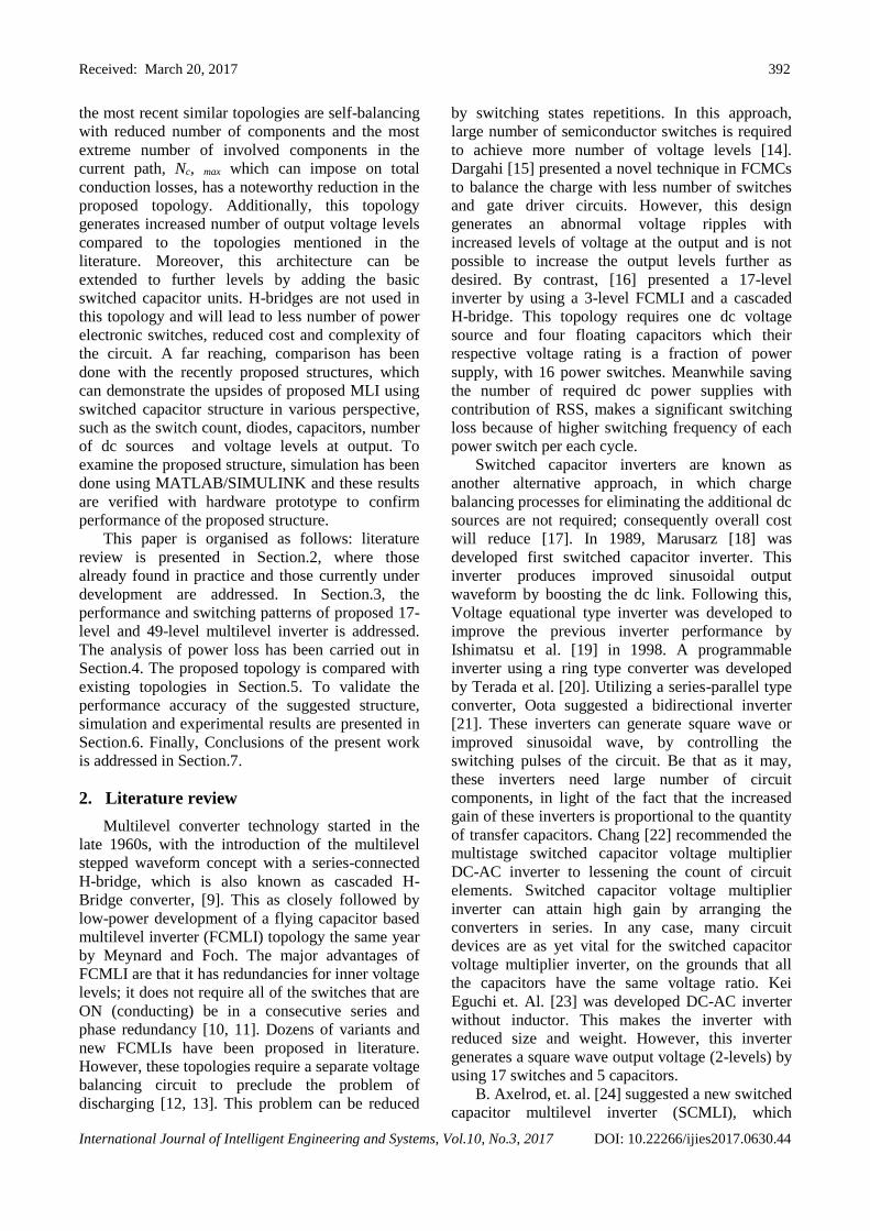
The basic architecture of proposed multilevel
Inverter is shown in Figure.2, which contains 2
switched capacitor units, 6 power semiconductor
switches, 2 dc sources and 2k (k is the half of the
isolated dc sources) capacitors. The number of
switches and power diodes required in the proposed
topology can be stated as following equations;
28 kNSwitch (1)
kNdiode 2 (2)
To generate maximum number of output levels 2
dc sources ae in asymmetric in nature. The
mathematical expression for the dc source of second
switched capacitor unit is given by,
1,2, )21( dc
kdc VV
(3)
The asymmetrical proposed topology will produce
maximum voltage levels at output can be expressed
as following,
122 221 kklevelN
(4)
The seventeen levels proposed inverter is shown
in Fig.3. This structure contains 10 power switches,
2 capacitors, 2 diodes and 2 isolated power supplies.
The value of DC sources of first SCU and second
SCU are Vdc and 3Vdc. The switching pattern of the
17-level topology is provided in Table. 1. For
example, if the value of Vdc is 10 V, and then the
+
-
+
-
+
-
Buy SmartDraw!- purchased copies print this
document without a watermark .
Visit www.smartdraw.com or call 1-800-768-3729.
+
-
+
-
+
-
Buy SmartDraw!- purchased copies print this
document without a watermark .
Visit www.smartdraw.com or call 1-800-768-3729.
+
-
+
-
+
-
Buy SmartDraw!- purchased copies print this
document without a watermark .
Visit www.smartdraw.com or call 1-800-768-3729.
Received: March 20, 2017 394
International Journal of Intelligent Engineering and Systems, Vol.10, No.3, 2017 DOI: 10.22266/ijies2017.0630.44
maximum voltage obtained at load is 80V. Each step
size is10 V. To get 80V at the output side SB1, S1,
ST, S’1, S’B1 should be turned ON. During this
period both the capacitors are in discharging mode.
When switches SB1, S2, ST, S’1, S’B1 are turn ON
simultaneously, the voltage at output will be 70 V
with capacitor C1 charging and C2 discharging.
The proposed topology can be extended to
further levels by adding SCU and switches. For
instant, by adding the one SCU and two switches to
the basic topology, will produce 49 level output.
Figure.2 Basic Proposed Switched Capacitor
Multilevel Inverter
Figure.3 Proposed Seventeen Level Multilevel
Inverter
Figure.4 49-level multilevel inverter
Hence, 49 level inverter require 14 switches, 3 DC
sources, 3 capacitors and 3 diodes. For example, the
switches SB1, ST2, ST, S’T1 alongside the internal
power switches of SCU-2 and SCU-3 and also
internal power switch of SCU-1 must be turn ON.
So as to generate 9th level of output, switches of SB1,
SB2, ST, S’T1 along with internal power switches of
SCU-3 and SCU-2 and also turn ON the SCU-1
switches which are in parallel. The switching
sequence is given in the Table. 2. To create higher
number of voltage levels at the output side with
regard to further levels, the value of additional dc
power sources of individually SC unit can be
implemented by the given expressions:
1)(2 )1(,1,, jrdcjdcjdc VVV
(5)
1)(2 )1(,,, jrdcjdcrjdc VVV
(6)
Table 1. Switching Sequence of Seventeen Level
Multilevel Inverter
S. No ON Switches Output Voltage Vo
1 SB1,S1,ST,S’1,S’B1 4Vdc+vc1+vc2
2 SB1,S2,ST,S’1,S’B1 4Vdc+vc2
3 ST1,S2,ST,S’1,S’B1 3Vdc+vc2
4 SB1,S1,ST,S’2,S’B1 4Vdc+vc2
5 SB1,S2,ST,S’2,S’B1 4Vdc
6 ST1,S2,ST,S’2,S’B1 3Vdc
7 SB1,S1,ST,S’2,S’T1 Vdc+vc1
8 SB1,S2,ST,S’2,S’T1 Vdc
9 SB1,S2,SB,S’2,S’B1 0
10 ST1,S2,SB,S’2,S’B1 -Vdc
11 ST1,S1,SB,S’2,S’B1 -Vdc-vc1
12 SB1,S2,SB,S’2,S’B1 -3Vdc
13 ST1,S2,SB,S’2,S’B1 -4Vdc
14 ST1,S1,SB,S’2,S’B1 -4Vdc-vc2
15 SB1,S2,SB,S’1,S’B1 -3Vdc-vc2
16 ST1,S2,SB,S’1,S’B1 -4Vdc-vc2
17 ST1,S1,SB,S’1,S’B1 -4Vdc-vc1-vc2
Table 2. Different states of switching of 49-Level
Multilevel Inverter
S. No ON Switches Output
Voltage, Vo
1 SB1,ST2,ST,S’T1 1,2
2 ST1,ST2,ST,S’B1 3,6
3 SB1,ST2,ST,S’B1 4,5,7,8
4 SB1,SB2,ST,S’T1 9,18
5 ST1,SB2,ST,S’B1 10,11,13,14,19,
20,22,23
6 SB1,SB2,ST,S’B1 12.15.21.24
7 ST1,SB2,ST,S’T1 16,17
+-
+-
+-
+
-
+
-
Buy SmartDraw!- purchased copies print this
document without a watermark .
Visit www.smartdraw.com or call 1-800-768-3729.
+-
+-
+-
+
-
+
-
Buy SmartDraw!- purchased copies print this
document without a watermark .
Visit www.smartdraw.com or call 1-800-768-3729.
+-
+-
+-
+
-
+
-
Buy SmartDraw!- purchased copies print this
document without a watermark .
Visit www.smartdraw.com or call 1-800-768-3729.
Received: March 20, 2017 395
International Journal of Intelligent Engineering and Systems, Vol.10, No.3, 2017 DOI: 10.22266/ijies2017.0630.44
4. Analysis of power loss for 17-level
suggested structure
The total power losses of this inverter includes:
Conduction losses Pc, Switching losses Psw, Losses
due to ripples in the capacitor. Fundamental
frequency of switching technique has been used to
calculate the above losses.
4.1 Losses due to switching
Switching losses take place for the period of ON
and OFF switching states. A linear approximation
between voltage and current of switches has been
assumed in the switching period. By using this
assumption, switching power losses can be
calculated for the ith switch as follows:
oniisw
t
onon
i
on
t
iswionsw
tIfV
ttt
It
t
iVswf
dttitvfP
on
on
,
0
0
,,,
6
1
dt ,
)()(
(7)
Where Vsw,i is the OFF state voltage of ith switch. I
and I’ are the ith switch current after turn ON and
before turn OFF respectively. The fundamental
switching frequency is denoted by f. Psw,on,i and
Psw,off,i are the switching power loss during ON and
OFF states.
offiisw
t
offoff
i
on
isw
t
iswioffsw
tIfV
ttt
It
t
Vf
dttitvfP
off
off
,
0
,
0
,,,
6
1
dt '
)()(
(8)
The total switching power losses is given by
ioffswionswsw PPP ,,.,
(9)
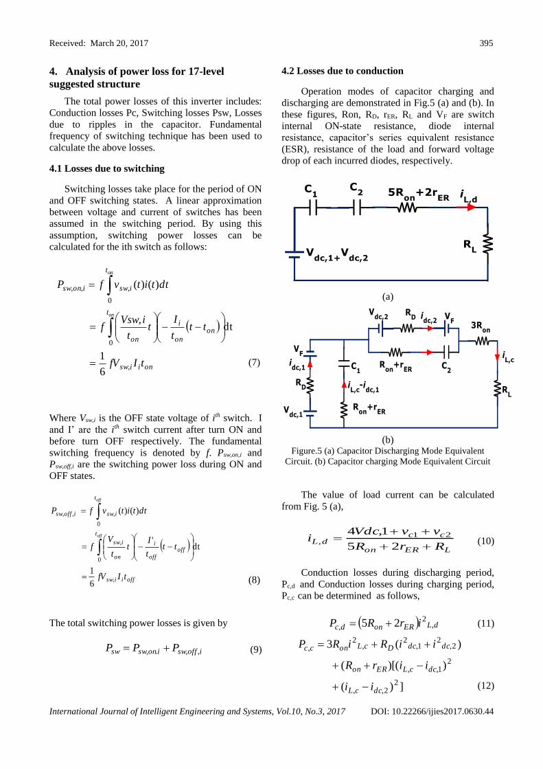
4.2 Losses due to conduction
Operation modes of capacitor charging and
discharging are demonstrated in Fig.5 (a) and (b). In
these figures, Ron, RD, rER, RL and VF are switch
internal ON-state resistance, diode internal
resistance, capacitor’s series equivalent resistance
(ESR), resistance of the load and forward voltage
drop of each incurred diodes, respectively.
(a)
(b)
Figure.5 (a) Capacitor Discharging Mode Equivalent
Circuit. (b) Capacitor charging Mode Equivalent Circuit
The value of load current can be calculated
from Fig. 5 (a),
LERon
ccdL
RrR
vvVdci
25
1,4 21,
(10)
Conduction losses during discharging period,
Pc,d and Conduction losses during charging period,
Pc,c can be determined as follows,
dLERondc irRP ,2
, 25
(11)
])(
))[((
)(3
22,,
21,,
2,2
1,2
,2
,
dccL
dccLERon
dcdcDcLoncc
ii
iirR
iiRiRP
(12)
Buy SmartDraw!- purchased copies print this
document without a watermark .
Visit www.smartdraw.com or call 1-800-768-3729.
Buy SmartDraw!- purchased copies print this
document without a watermark .
Visit www.smartdraw.com or call 1-800-768-3729.
Received: March 20, 2017 396
International Journal of Intelligent Engineering and Systems, Vol.10, No.3, 2017 DOI: 10.22266/ijies2017.0630.44
Therefore, the total conduction losses is given by
Lrmsonccdcc IRPPP ,
2,, 3
(13)
Where Irms, L is the load current rms value.
4.3 Losses due to ripple
During charging operation of the capacitors, the
difference between the respected input voltage and
the voltage of capacitors (Vci (i=1, 2)) [25] causes
arising of ripple losses. Thus, the capacitor voltage
ripple ΔVci is given by
dtti
CV
t
t
Cii
Ci )(1
'
(14)
Where, iCi (t) is the current of capacitor and the
time interval for discharging modes is [t’ − t],
which can be obtained by regarding to Table 1. Thus,
the total value of ripple loss, for one full cycle of
output waveform is equal to
2
1
2
2i
ciirip VCf
P
(15)
The total loss of the suggested topology is the
sum of switching, conduction and ripples losses and
is expressed as follows,
ripcswlosses PPPP
(16)
Overall efficiency can be calculated as,
lossesout
out
PP
P
(17)
5. Comparison of proposed structure with
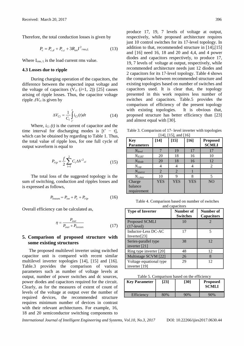
some existing structures
The proposed multilevel inverter using switched
capacitor unit is compared with recent similar
multilevel inverter topologies [14], [15] and [16].
Table.3 provides the comparison of various
parameters such as number of voltage levels at
output, number of power switches and dc sources,
power diodes and capacitors required for the circuit.
Clearly, as for the measures of extent of count of
levels of the voltage at output over the number of
required devices, the recommended structure
requires minimum number of devices in contrast
with their relevant architectures. For example, 16,
18 and 20 semiconductor switching components to
produce 17, 19, 7 levels of voltage at output,
respectively, while proposed architecture requires
just 10 control switches for its 17-level topology. In
addition to that, recommended structure in [14],[15]
and [16] need 16, 18 and 20 and 4,4, and 4 power
diodes and capacitors respectively, to produce 17,
19, 7 levels of voltage at output, respectively, while
recommended architecture needs just 12 diodes and
2 capacitors for its 17-level topology. Table 4 shows
the comparison between recommended structure and
existing topologies based on number of switches and
capacitors used. It is clear that, the topology
presented in this work requires less number of
switches and capacitors. Table.5 provides the
comparison of efficiency of the present topology
with existing topologies. It is obvious that,
proposed structure has better efficiency than [23]
and almost equal with [30].
Table 3. Comparison of 17- level inverter with topologies
[14], [15], and [16]
Key
Parameters
[14] [15] [16] Proposed
SCMLI
Nlevel 7 19 17 17
NIGBT 20 18 16 10
Ndiode 20 18 16 12
Ncap 4 4 4 2
Nsource 2 2 1
Nc,max 10 9 8 5
Charge
balance
requirement
YES YES YES NO
Table 4. Comparison based on number of switches
and capacitors
Type of Inverter Number of
Switches
Number of
Capacitors
Proposed SCMLI
(17-level)
10 2
Inductor-Less DC-AC
Inverter[23]
17 5
Series-parallel type
inverter [21]
38 12
Ring type inverter [20] 48 12
Multistage SCVM [22] 26 8
Voltage equational type
inverter [19]
29 12
Table 5. Comparison based on the efficiency
Key Parameter [23] [30] Proposed
SCMLI
Efficiency 80% 90% 90%
Received: March 20, 2017 397
International Journal of Intelligent Engineering and Systems, Vol.10, No.3, 2017 DOI: 10.22266/ijies2017.0630.44
(a)
(b)
Figure.6 Simulation waveforms of 17-level multilevel
inverter (a) output voltage wave form (b) Current
waveform
6. Simulation and experimental results
To analyse the performance of recommended
switching capacitor based multilevel inverter, the
simulation and experimental results of 17-level
inverter are presented. MATLAB/Simulink has been
used for simulation. In addition to that, the
hardware prototype of seventeen-level inverter with
80 V has been developed. The FPGA spartan-3e has
been used to produce the gating pulses. For the
present structure fundamental switching frequency
method is used. The MOSFETs used are IRF-840,
500 V, 8A and Ron is 0.85 and Power diodes
used are FR107, 700 V and 50 . Capacitors have
been used with 4700 F and 50 V. The prototype has
been tested on R-L load with the magnitude of 0.5
mH and 500 for all the studies.
In this topology, the values of dc sources are
unequal and are 10 V and 30 V. According to this
present topology produces the maximum voltage at
the output will be 80 V. R-L load have been used for
both simulation and experimental tests. The
simulation results of proposed multilevel inverter
which produces 17-level have shown in Fig.6 (a)
and (b). It is observed that the output voltage is 80
V and current is 950 mA.
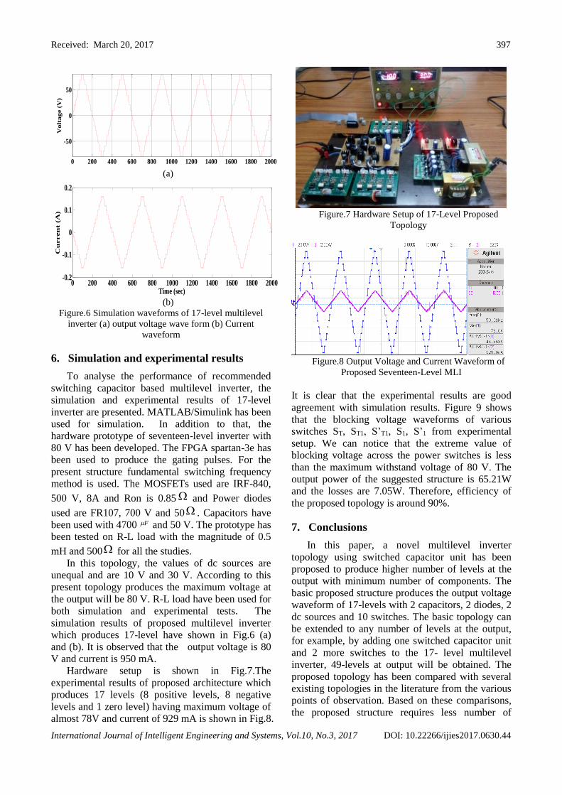
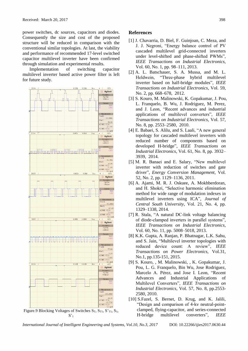
Hardware setup is shown in Fig.7.The
experimental results of proposed architecture which
produces 17 levels (8 positive levels, 8 negative
levels and 1 zero level) having maximum voltage of
almost 78V and current of 929 mA is shown in Fig.8.
Figure.7 Hardware Setup of 17-Level Proposed
Topology
Figure.8 Output Voltage and Current Waveform of
Proposed Seventeen-Level MLI
It is clear that the experimental results are good
agreement with simulation results. Figure 9 shows
that the blocking voltage waveforms of various
switches ST, ST1, S’T1, S1, S’1 from experimental
setup. We can notice that the extreme value of
blocking voltage across the power switches is less
than the maximum withstand voltage of 80 V. The
output power of the suggested structure is 65.21W
and the losses are 7.05W. Therefore, efficiency of
the proposed topology is around 90%.
7. Conclusions
In this paper, a novel multilevel inverter
topology using switched capacitor unit has been
proposed to produce higher number of levels at the
output with minimum number of components. The
basic proposed structure produces the output voltage
waveform of 17-levels with 2 capacitors, 2 diodes, 2
dc sources and 10 switches. The basic topology can
be extended to any number of levels at the output,
for example, by adding one switched capacitor unit
and 2 more switches to the 17- level multilevel
inverter, 49-levels at output will be obtained. The
proposed topology has been compared with several
existing topologies in the literature from the various
points of observation. Based on these comparisons,
the proposed structure requires less number of
0 200 400 600 800 1000 1200 1400 1600 1800 2000
-50
0
50
Time (sec)
Vo
lta
ge (
V)
0 200 400 600 800 1000 1200 1400 1600 1800 2000-0.2
-0.1
0
0.1
0.2
Time (sec)
Cu
rren
t (
A)
Received: March 20, 2017 398
International Journal of Intelligent Engineering and Systems, Vol.10, No.3, 2017 DOI: 10.22266/ijies2017.0630.44
power switches, dc sources, capacitors and diodes.
Consequently the size and cost of the proposed
structure will be reduced in comparison with the
conventional similar topologies. At last, the viability
and performance of recommended 17-level switched
capacitor multilevel inverter have been confirmed
through simulation and experimental results.
Implementation of switching capacitor
multilevel inverter based active power filter is left
for future study.
Figure.9 Blocking Voltages of Switches ST, ST1, S’T1, S1,
S’1
References
[1] J. Chavarria, D. Biel, F. Guinjoan, C. Meza, and
J. J. Negroni, “Energy balance control of PV
cascaded multilevel grid-connected inverters
under level-shifted and phase-shifted PWMs”,
IEEE Transactions on Industrial Electronics,
Vol. 60, No. 1, pp. 98–111, 2013.
[2] A. L. Batschauer, S. A. Mussa, and M. L.
Heldwein, “Three-phase hybrid multilevel
inverter based on half-bridge modules”, IEEE
Transactions on Industrial Electronics, Vol. 59,
No. 2, pp. 668–678, 2012.
[3] S. Kouro, M. Malinowski, K. Gopakumar, J. Pou,
L. Franquelo, B. Wu, J. Rodriguez, M. Perez,
and J. Leon, “Recent advances and industrial
applications of multilevel converters”, IEEE
Transactions on Industrial Electronics, Vol. 57,
No. 8, pp. 2553–2580, 2010.
[4] E. Babaei, S. Alilu, and S. Laali, “A new general
topology for cascaded multilevel inverters with
reduced number of components based on
developed H-bridge”, IEEE Transactions on
Industrial Electronics, Vol. 61, No. 8, pp. 3932–
3939, 2014.
[5] M. R. Banaei and E. Salary, “New multilevel
inverter with reduction of switches and gate
driver”, Energy Conversion Management, Vol.
52, No. 2, pp. 1129–1136, 2011.
[6] A. Ajami, M. R. J. Oskuee, A. Mokhberdoran,
and H. Shokri, “Selective harmonic elimination
method for wide range of modulation indexes in
multilevel inverters using ICA”, Journal of
Central South University, Vol. 21, No. 4, pp.
1329–1338, 2014.
[7] R. Stala, “A natural DC-link voltage balancing
of diode-clamped inverters in parallel systems”,
IEEE Transactions on Industrial Electronics,
Vol. 60, No. 11, pp. 5008–5018, 2013.
[8] K.K. Gupta, A. Ranjan, P. Bhatnagar, L.K. Sahu,
and S. Jain, “Multilevel inverter topologies with
reduced device count: A review”, IEEE
Transactions on Power Electronics, Vol.31,
No.1, pp.135-151, 2015.
[9] S. Kouro, , M. Malinowski, , K. Gopakumar, J.
Pou, L. G. Franquelo, Bin Wu, Jose Rodriguez,
Marcelo A. Pérez, and Jose I. Leon, “Recent
Advances and Industrial Applications of
Multilevel Converters”, IEEE Transactions on
Industrial Electronics, Vol. 57, No. 8, pp.2553-
2580, 2010.
[10] S.Fazel, S. Bernet, D. Krug, and K. Jalili,
“Design and comparison of 4-kv neutral-point-
clamped, flying-capacitor, and series-connected
H-bridge multilevel converters”, IEEE

Received: March 20, 2017 399
International Journal of Intelligent Engineering and Systems, Vol.10, No.3, 2017 DOI: 10.22266/ijies2017.0630.44
Transactions on Industrial Electronics, Vol. 43,
No. 4, pp. 1032–1040, 2007.
[11] K. D. Papastergiou, P. W. Wheeler, and J. C.
Clare, “Comparison of losses in multilevel
converters for aerospace applications”, In: Proc.
IEEE Power Electron. Specialist Conf., pp.
4307–4312, 2008.
[12] B. P. McGrath and D. G. Holmes, “Analytical
modelling of voltage balance dynamics for a
flying capacitor multilevel converter”, IEEE
Transactions on Power Electronics, Vol. 23, No.
2, pp. 543–550, 2008.
[13] M. Khazraei, H. Sepahvand, K. A. Corzine, and
M. Ferdowsi, “Active capacitor voltage
balancing in single-phase flying-capacitor
multilevel power converters”, IEEE
Transactions on Industrial Electronics, Vol. 59,
No. 2, pp. 769– 778, 2012.
[14] V. Dargahi, A. K. Sadigh, M. Abarzadeh, S.
Eskandari, and K. Corzine, “A new family of
modular multilevel converter based on modified
flying capacitor multi cell converters”, IEEE
Transactions on Power Electronics, Vol. 30, No.
1, pp. 138–147, 2015.
[15] V. Dargahi, A. K. Sadigh, M. Abarzadeh, M. R.
A. Pahlavani, and A. Shoulaie, “Flying
capacitor reduction in an improved double
flying capacitor multi-cell converter controlled
by a modified modulation method”, IEEE
Transactions on Power Electronics, Vol. 27, No.
9, pp. 3875–3887, 2012.
[16] P. Roshankumar, R. S. Kaarthic, K. Gupakumar,
J. I. Leon, and L. G. Franquelo,“ A seventeen-
level inverter formed by cascading flying
capacitor and floating capacitor H-bridge”,
IEEE Transactions on Power Electronics, Vol.
30, No. 7, pp. 3471–3478, 2015.
[17] M. S.W. Chan and K. T. Chau, “A new
switched-capacitor boost multilevel inverter
using partial charging”, IEEE Trans. Circuits
Syst. II, Exp. Briefs, Vol. 54, No. 12, pp. 1145–
1149, 2007.
[18] R. Marusarz, “A switched capacitor, inductor
less DC to AC voltage step-up power
converter”, In: Proc. of the 20th Annual Power
Electronics Specialists Conf., pp.99-103, 1989.
[19] K. Ishimatsu, I. Oota, and F. Ueno. “A DC-AC
converter using a voltage equational type
switched-capacitor transformer”, In: Proc. of
the Thirteenth Annual Applied Power
Electronics Conf. and Exposition, APEC’98,
Vol. 2, pp. 603-606, 1998.
[20] S. Terada, I. Oota, K. Eguchi, and F. Ueno. “A
ring type switched-capacitor (SC)
programmable converter with DC or AC input/
DC or AC output”, In: Proc. of the 47th IEEE
International Midwest Symposium on Circuits
and Systems., pp. I-29 – I-32, 2004.
[21] M. Oota, S. Terada, K. Eguchi, and I. Oota.
“Development of switched-capacitor bi-
directional DC-AC converter for inductive and
capacitive loads”, In: Proc. of IEEE
International Symposium on Industrial
Electronics., pp. 1618-1623, 2009.
[22] Y. H. Chang, “Modelling and analysis of
multistage switched-capacitor-voltage-
multiplier boost DC-AC inverter”, In: Proc. of
IEEE 9th International Conf. on Power
Electronics and Drive Systems, PEDS 2011, pp.
523- 526, 2011.
[23] K. Eguchi, K. Abe and W. Do, “Synthesis and
Analysis of a Simple Inductor-Less DC-AC
Inverter”, In: Proc. of 6th International
Workshop on Computer Science and
Engineering, pp.315-319, 2016.
[24] B. Axelrod, Y. Berkovich, and A. Ioinovici, “A
cascade boost switched capacitor-converter
two-level inverter with an optimized multilevel
output waveform”, IEEE Transactions on
Circuits Syst. I, Vol. 52, No. 12, pp. 2763–2770,
2005.
[25] Y. Hinago and H. Koizumi, “A switched-
capacitor inverter using series/ parallel
conversion with inductive load”, IEEE
Transactions on Industrial Electronics, Vol. 59,
No. 2, pp. 878–887, 2012.
[26] J. Liu, K. W. E, Cheng, and Y. Ye, “A
cascaded multilevel inverter based on switched-
capacitor for high-frequency ac power
distribution system”, IEEE Transactions on
Power Electronics, Vol. 22, No. 8, pp 4219–
4230, 2014.
[27] E. Babaei and F. Sedaghati, “Series-parallel
switched-capacitor based multilevel inverter”,
In: Proc. Int. Conf. Electr. Mach. Syst., pp 1–5,
2011.
[28] Y. Ye, K. Cheng, J. Liu, and K. Ding, “A step-
up switched-capacitor multilevel inverter with
self-voltage balancing”, IEEE Transactions on
Industrial Electronics, Vol. 61, No. 12, pp.
6672–6680, 2014.
[29] E. Babaei and S. S. Gowgani, “Hybrid
multilevel inverter using switched capacitor
units”, IEEE Transactions on Industrial
Electronics, Vol. 61, No. 9, pp. 4614–4621,
2014.
[30] K. Eguchi, K. Abe, W. Do and H. Sasaki,
“Design of Inductor-Less DC-AC Inverter
Using A step-Down Fibonacci Sequence

Received: March 20, 2017 400
International Journal of Intelligent Engineering and Systems, Vol.10, No.3, 2017 DOI: 10.22266/ijies2017.0630.44
Generator”, ICICI Express Letters, Vol.10.
No.8, pp.1951-1956, 2016.