Embed Size (px)
Citation preview

University of Tennessee, Knoxville University of Tennessee, Knoxville
TRACE: Tennessee Research and Creative TRACE: Tennessee Research and Creative
Exchange Exchange
Doctoral Dissertations Graduate School
12-2011
Design and Control of High Power Density Motor Drive Design and Control of High Power Density Motor Drive
Dong Jiang [email protected]
Follow this and additional works at: https://trace.tennessee.edu/utk_graddiss
Part of the Controls and Control Theory Commons, Electrical and Electronics Commons, and the
Power and Energy Commons
Recommended Citation Recommended Citation Jiang, Dong, "Design and Control of High Power Density Motor Drive. " PhD diss., University of Tennessee, 2011. https://trace.tennessee.edu/utk_graddiss/1196
This Dissertation is brought to you for free and open access by the Graduate School at TRACE: Tennessee Research and Creative Exchange. It has been accepted for inclusion in Doctoral Dissertations by an authorized administrator of TRACE: Tennessee Research and Creative Exchange. For more information, please contact [email protected].

To the Graduate Council:
I am submitting herewith a dissertation written by Dong Jiang entitled "Design and Control of
High Power Density Motor Drive." I have examined the final electronic copy of this dissertation
for form and content and recommend that it be accepted in partial fulfillment of the
requirements for the degree of Doctor of Philosophy, with a major in Electrical Engineering.
Fred Wang, Major Professor
We have read this dissertation and recommend its acceptance:
Leon. M. Tolbert, Yilu Liu, Rao. V. Arimilli
Accepted for the Council:
Carolyn R. Hodges
Vice Provost and Dean of the Graduate School
(Original signatures are on file with official student records.)

Design and Control of High Power Density Motor Drive
A Dissertation Presented for the
Doctor of Philosophy
Degree in Electrical Engineering
The University of Tennessee, Knoxville
Dong Jiang
Dec. 2011

ii
Acknowledgements
This dissertation is the work under the advisory of my supervisor Dr. Fred Wang. First, I want
to show my endless gratitude to him, for his patience, support and guidance during my PhD
study as well as my PhD life. Beyond numerous specific technical problems, he also helped me
to find the way to face the challenges and opportunities in my life and do my best to achieve the
final goals. His profound knowledge, gentle personality and rigorous attitude toward research
will benefit my career as well as my whole personal life. I also want to thank the opportunities
he provided for me to be able to work in two great campuses.
I also want to show my gratitude to the other PhD dissertation committee members. Many
thanks to Dr. Leon Tolbert for his help in my research in the power electronics lab in the
University of Tennessee (UTK), and his guidance for my dissertation. I also want to thank Dr.
Yilu Liu and Dr. Rao Arimilli for their help in my dissertation. Their expertise in power
engineering and mechanics help me to improve the dissertation.
I am so lucky to be able to work in two great campuses for my PhD dissertation, and
supported by two NSF research centers. Some of the dissertation works were fulfilled in the
Center for Power Electronics Systems (CPES) in Virginia Polytechnic Institute and State
University (VT) from 2007 to 2010. I would like to thank Dr. Dushan Boroyevich and Dr.
Rolando Burgos, for their advisory and support for my dissertation work in CPES. Also, I want
to thank Dr. Krishnan Ramu in VT for his guidance and support from 2009 to 2010.
I would like to thank the National Science Foundation (NSF), the Boeing Company, and the
Department of Energy for their financial support for my PhD life. I would also want to thank
people in the University of Wisconsin-Madison (UW) for their efforts for our collaborated
projects which contributed to this dissertation.

iii
I would like to thank all my colleagues in UTK for their help not only for the research work
but also daily life. I cherish the great time we worked together. They are Miss Shengnan Li, Mr.
Faete Filho, Mr. Mihat Can Kisacikoglu, Miss Lakshmi Reddy, Mr. Fan Xu, Mr. Weimin Zhang,
Miss Bailu Xiao, Miss Yutian Cui, Miss Jing Wang, Mr. Yiwei Ma, Mr. Wenchao Cao, Mr.
Zheyu Zhang, and Mr. Yalong Li. My special thanks are to Dr. Ming Li, Miss Zhuxian Xu, Mr.
Jing Xue and Mr. Ben Guo for their cooperation in the dissertation work.
I would also like to thank my colleagues in VT for their help in my PhD life from 2007 to
2010. I could not list all their names for thanks, but I would like to show my special thanks to Dr.
Rixin Lai, Dr. Shuo Wang, Dr. Di Zhang, Dr. Puqi Ning, Mr. Ruxi Wang, Dr. Fang Luo, Dr.
Gerald Francis, Mr. Zhiyu Shen, Mr. Zheng Chen and Mr. Dong Dong for their cooperation and
help in my dissertation work. I would also like to thank Mr. Tong Liu, Mr. Daocheng Huang, Mr.
Qian Li, Dr. Xiao Cao, Mr. Zijian Wang, Mr. Feng Yu, Mr. Mingkai Mu, Mr. Yi Sun, Dr. Pengju
Kong, Dr. Dianbo Fu and so many friends in CPES for their kind help especially in my hard time.
So many staff members gave me so much help during my four and half years’ life in the USA.
I would show my special thanks to Ms. Dana Bryson and Mr. William Rhodes in UTK and Mr.
Robert Martin, Ms. Teresa Shaw, Mr. Douglas Sterk and Ms. Marianne Hawthorne in VT for
their kind help during my PhD life.
My last and the most affected thanks are to my parents, Shengan Jiang and Zhaohui Liao for
their 28 years continuous love and support for me. Although I spent too little time with them the
past 10 years, I use this dissertation as my best gift for them.

iv
Abstract
This dissertation aims at developing techniques to achieve high power density in motor drives
under the performance requirements for transportation system. Four main factors influencing the
power density are the main objects of the dissertation: devices, passive components, pulse width
modulation (PWM) methods and motor control methods.
Firstly, the application of SiC devices could improve the power density of the motor drive.
This dissertation developed a method of characterizing the SiC device performance in phase-leg
with loss estimation, and claimed that with SiC Schottky Barrier Diode the advantage of SiC
JFET could benefit the motor drive especially at high temperature.
Then the design and improvement of the EMI filter in the active front-end rectifier of the
motor drive was introduced in this dissertation. Besides the classical filter design method, the
parasitic parameters in the passive filter could also influence the filtering performance. Random
PWM could be applied to reduce the EMI noise peak value.
The common-mode (CM) noise reduction by PWM methods is also studied in this dissertation.
This dissertation compared the different PWM methods’ CM filtering performance. Considering
the CM loop, the design of PWM methods and switching frequency should be together with the
CM impedance.
Variable switching frequency PWM (VSFPWM) methods are introduced in the dissertation
for the motor drive’s EMI and loss improvement. The current ripple of the three-phase converter
could be predicted. Then the switching frequency could be designed to adapt the current ripple
requirements. Two VSFPWM methods are introduced to satisfy the ripple current peak and RMS
value requirements.

v
For motor control issue, this dissertation analyzed the principle of the start-up transient and
proposed an improved start-up method. The transient was significantly reduced and the motor
could push to high speed and high power with speed sensorless control.
Next, the hardware development of modular motor drive was introduced. The development
and modification of 10kW phase-legs and full power test of a typical 30kW modular converter is
realized with modular design method.
Finally, the techniques developed in this dissertation for high power density motor drive
design and control are summarized and future works are proposed.

vi
Table of Contents
Acknowledgements ......................................................................................................................... ii
Abstract .......................................................................................................................................... iv
List of Tables ................................................................................................................................. ix
List of Figures ................................................................................................................................. x
Chapter 1. Introduction ................................................................................................................... 1
1.1 Research background ........................................................................................................... 1
1.2 Current technical status ......................................................................................................... 6
1.2.1 Power electronics devices ............................................................................................... 7
1.2.2 Passive components ........................................................................................................ 8
1.2.3 Pulse width modulation (PWM) methods on density and efficiency ............................. 9
1.2.4 Motor control techniques .............................................................................................. 11
1.2.5 Hardware status ............................................................................................................ 13
1.3 Research challenges and objectives ................................................................................... 14
1.4 Organization of the dissertation ......................................................................................... 17
Chapter 2. SiC Devices Analysis in Motor Drive ......................................................................... 20
2.1 Introduction of SiC devices ................................................................................................ 20
2.2 SiC devices conduction performance evaluation ............................................................... 24
2.3 SiC devices switching performance evaluation ................................................................. 26
2.4 Device and converter loss estimation ................................................................................. 34
2.5 Conclusions ........................................................................................................................ 42
Chapter 3. EMI Noise Attenuation for the Active Front-end Rectifier ........................................ 44
3.1 Introduction ........................................................................................................................ 44
3.2 Input EMI filter design ....................................................................................................... 47
3.3 Coupling issue for input EMI filter .................................................................................... 52
3.4 Input EMI noise reduction by Random PWM ................................................................... 54
3.5 Conclusions ........................................................................................................................ 60
Chapter 4. Common-mode EMI Noise Attenuation for the Inverter ........................................... 62
4.1 Introduction ........................................................................................................................ 62

vii
4.2 Different PWM Methods on the Noise Source .................................................................. 65
4.2.1 CM noise source analysis ............................................................................................. 65
4.2.2 CM noise current analysis ............................................................................................ 70
4.2.3 CM choke volt-seconds analysis .................................................................................. 75
4.3 Experimental verification ................................................................................................... 79
4.4 Conclusions ........................................................................................................................ 85
Chapter 5. Variable Switching Frequency PWM for Loss and EMI Improvement ...................... 88
5.1 Introduction ......................................................................................................................... 88
5.2 Analytical Current Ripple Analysis for Three-phase PWM converter ............................... 90
5.3 Ripple current comparison .................................................................................................. 96
5.4 Variable Switching Frequency PWM Control Architecture ............................................. 102
5.5 Variable Switching Frequency PWM to Control Peak Current Ripple (VSFPWM1) ...... 104
5.6 Variable Switching Frequency PWM to Control Ripple Current RMS Value (VSFPWM2) ................................................................................................................................................. 110
5.7 Experimental Verification ................................................................................................. 114
5.8 Conclusions ....................................................................................................................... 122
Chapter 6. Permanent Magnet Motor Control with High Density Motor Drive ......................... 124
6.1 Introduction ...................................................................................................................... 124
6.2 Speed sensorless control method for PM motor............................................................... 126
6.3 Improvement for start-up transient ................................................................................... 131
6.4 Experiments ...................................................................................................................... 138
6.5 Conclusions ...................................................................................................................... 142
Chapter 7. Modular Motor Drive Design and Development ..................................................... 144
7.1 Introduction ...................................................................................................................... 144
7.2 System configuration and interface .................................................................................. 146
7.3 Hardware design and construction ................................................................................... 148
7.3.1 Controller .................................................................................................................... 149
7.3.2 Mother board .............................................................................................................. 151
7.3.3 Phase-leg module ........................................................................................................ 152
7.3.4 System assembly......................................................................................................... 153
7.4 Phase-leg module development ........................................................................................ 155

viii
7.5 Converter Test ................................................................................................................... 157
7.6 Conclusions ....................................................................................................................... 159
Chapter 8. Conclusions and Future Work ................................................................................... 161
8.1 Conclusions ...................................................................................................................... 161
8.2 Future work ...................................................................................................................... 163
References ................................................................................................................................... 165
VITA ........................................................................................................................................... 174

ix
List of Tables Table 1-1. Estimated motor drive numbers and rating for a typical MEA[5] 2
Table 1-2. Demo motor drives with SiC devices developed in recent years 8
Table 2-1. Conduction loss power of JFET 26
Table 2-2. Switching loss with 600V voltage 27
Table 2-3. Rated value of 10kW AC-DC-AC converter 38
Table 3-1. Theoretical terminal phase voltage of Vienna-type rectifier in each switching cycle 56
Table 5-1. Ripple current slope with different voltage vectors 93
Table 6-1. Parameters of the two AFPM motors in the experiments 131
Table 6-2. Function of each region in the proposed start-up process 135
Table 7-1. Main components weight estimation 154

x
List of Figures Figure 1-1. AC-fed motor drive 4
Figure 1-2. DC-fed motor drive 4
Figure 1-3. DC-fed motor drive 6
Figure 2-1. Structure of SiC Schottky diode 22
Figure 2-2. Structure of SiC JFET 22
Figure 2-3. SiC JFET conduction performance in D-S (left) and S-D (right) direction from 250C-
2000C 24
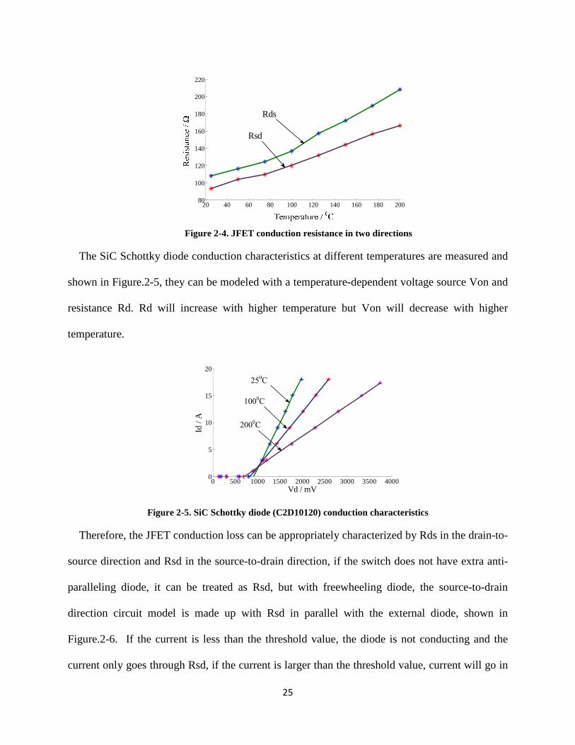
Figure 2-4. JFET conduction resistance in two directions 25
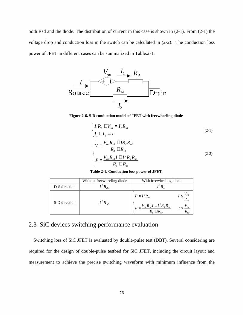
Figure 2-5. SiC Schottky diode (C2D10120) conduction characteristics 25
Figure 2-6. S-D conduction model of JFET with freewheeling diode 26
Figure 2-7. SiC JFET bridge test circuit 27
Figure 2-8. High temperature experimental set-up of switching test 29
Figure 2-9. Actual testbed for high temperature switching experiments 29
Figure 2-10. Switching waveform of JFET bridge 31
Figure 2-11. Turn-on (a) and turn-off (b) waveform in the bridge with only JFET at 250C, 1000C,
2000C: With 10 Ω gate resistance 33
Figure 2-12. Turn-on (a) and turn-off (b) waveform in the bridge with paralleled SiC Schottky
diodes at 250C, 1000C,2000C: With 10 Ω gate resistance 34
Figure 2-13. Voltage/current definition in phase-leg (a) and general switching waveforms for
switch 1 turn-on (b) and turn-off (c) 35
Figure 2-14. Switching loss linearization 37
Figure 2-15. Case1 of AC-DC-AC converter: without freewheeling diode 38
Figure 2-16. Case2 of AC-DC-AC converter: with freewheeling diode 38
Figure 2-17. Duty cycle of minimum losses DPWM 38
Figure 2-18. Converter conduction losses at 250C (left) and 2000C (right) 40
Figure 2-19. Converter switching losses at 250C (left) and 2000C (right) 40
Figure 2-20. Inverter and rectifier total losses at 250C (left) and 2000C (right) 41

xi
Figure 2-21. Loss distribution of AC-DC-AC converter at 2000C with case 1 (left, total loss
537W) and case 2 (right, total loss 365W) 41
Figure 2-22. Efficiency at different power for the AC-DC-AC converter : (a) 250C, (b) 2000C 42
Figure 3-1. D6-16050-5 EMI standard 47
Figure 3-2. Vienna-type rectifier based on SiC devices 47
Figure 3-3. Three-stage L-CL-CL filter 48
Figure 3-4. Noise conducting path in the Vienna-type rectifier input filter 49
Figure 3-5. DM filter equivalent circuit 49
Figure 3-6. CM filter equivalent circuit 49
Figure 3-7. Two-stage filter damping principle 50
Figure 3-8. Dimension of torrid core 50
Figure 3-9. Nanocrystalline core (a), type 1 inductor (b) and type 2 inductor (c) 51
Figure 3-10. Coupling in the three-stage filter 52
Figure 3-11. Influence of coupling inductance on attenuation 53
Figure 3-12 Three different set-up of the filter: (a) C2 close to inductor, (b) C2 on different side
from L2, (c) C2 far away from the inductor 53
Figure 3-13. Comparison of the EMI in the three different set-ups of the filter 54
Figure 3-14. Theoretical calculation results of phase voltage of Vienna rectifier with 70kHz
SVPWM, 40kHz SVPWM and RPWM (55kHz~70kHz) : (a)Waveform and (b) Spectrum 56
Figure 3-15. Simulation results of current spectrum in A and dBµA of the Vienna rectifier with
only boost inductor and using 70 kHz SVPWM 57
Figure 3-16. Simulation results of current spectrum in A and dBµA of the Vienna rectifier with
only boost inductor and using 55 kHz~70 kHz RPWM 57
Figure 3-17. Experimental results of Vienna-type Rectifier with 70 kHz SVPWM (a), 40 kHz
SVPWM (b) and 55~70 kHz RPWM (c) 59
Figure 3-18. Fourier analysis results of the current and voltage of Vienna-type Rectifier: with 70
kHz SVPWM (a), 40 kHz SVPWM (b) and 55~70 kHz RPWM (c) 60
Figure 3-19. Experimental results: EMI measurement results of three cases with three-stage filter,
330V DC voltage and 3.6 kW output power 60

xii
Figure 4-1. AC-fed motor drive with grounding 63
Figure 4-2. DC-fed motor drive with grounding 63
Figure 4-3. Equivalent circuit for VSI based motor drive CM path: (a) three-phase equivalent
circuit (b) CM path 64
Figure 4-4. Gate logic and CM voltage for: (a) SVPWM; (b) DPWM (clamped to positive bus);
(c) DPWM (clamped to negative bus); (d) AZSPWM; (e) NSPWM 66
Figure 4-5. Comparison of the modulation signals 67
Figure 4-6. CM modulation signal for SPWM, SVPWM and DPWM with modulation index of
(a):0.9, (b):0.6, (c):0.3 67
Figure 4-7. Spectrum analysis for CM modulation signals (f=400Hz) for (a) SVPWM and (b)
DPWM 67
Figure 4-8. Comparison of spectrum of CM modulation signal between SVPWM and DPWM
with m=0.9 68
Figure 4-9. CM loop current transfer gain with typical parameters 69
Figure 4-10. CM voltage and its spectrum with 400Hz fundamental frequency and m=0.9 (a)
SVPWM vs.AZSPWM and (b) DPWM vs. NSPWM 69
Figure 4-11. CM voltage and its spectrum with 400Hz fundamental frequency and m=0.3 (a)
SVPWM vs. AZSPWM and (b) DPWM vs. NSPWM 70
Figure 4-12. CM current comparison between NSPWM and DPWM (m=0.9) with switching
frequency: (a) 12.5kHz, (b) 40kHz 72
Figure 4-13. CM current comparison between AZSPWM and SVPWM (m=0.3) with switching
frequency: (a) 7kHz, (b) 20kHz 73
Figure 4-14. CM voltage spectrum comparison (f=300Hz,fs=20kHz,m=0.3) 73
Figure 4-15. CM current comparison between SVPWM and DPWM (m=0.3) with (a) Cs=10nF,
(b) Cs=30nF 74
Figure 4-16. Three-phase CM choke structure 75
Figure 4-17. Volt-seconds demonstration for the CM voltage source in one switching cycle: (a)
SPWM; (b) SVPWM; (c) DPWM 76
Figure 4-18. Source CM volt-seconds comparison (a): SVPWM; (b): DPWM 77

xiii
Figure 4-19. Source CM volt-seconds (m=0.9) comparison (a): SVPWM vs. AZSPWM; (b):
DPWM vs. NSPWM 77
Figure 4-20. Frequency domain bode plot of (a) voltage drop on CM choke (b) CM choke volt-
seconds 78
Figure 4-21. Experimental circuit for CM noise 79
Figure 4-22. PWM generation diagram for experiments 79
Figure 4-23. Details of three-phase output voltage and CM voltage for (a): AZSPWM (b):
NSPWM 80
Figure 4-24. Experimental results: CM voltage comparison with m=0.9, 6 kHz switching
frequency and 60 Hz fundamental frequency (a): time domain (b): spectrum 81
Figure 4-25. Experimental results: comparison of CM voltage between SVPWM and AZSPWM
(m=0.3) 81
Figure 4-26. CM loop transadmittance for the experimental system 82
Figure 4-27. CM current comparison between DPWM and NSPWM (a): fs=6 kHz (b): fs=20
kHz 83
Figure 4-28. CM current comparison between SVPWM and AZSPWM (a): fs=3.6 kHz (b):
fs=20 kHz 83
Figure 4-29. Conducted EMI comparison (fs=20 kHz), (a): SVPWM vs. AZSPWM; (b): DPWM
vs. NSPW 84
Figure 4-30. Comparison of CM current between SVPWM and DPWM with low modulation
index (m=0.3) (a): Cs=10 nF, (b): Cs=30 nF, (c): Cs=50 nF 85
Figure 5-1. 7 sectors in one switching cycle in SVPWM 91
Figure 5-2. Ripple current variation in one switching cycle in SVPWM 91
Figure 5-3. Switch combination of 8 different voltage vectors and their Thevenin equivalent
circuits 92
Figure 5-4. Current ripple in one switching cycle: SVPWM 94
Figure 5-5. Current ripple in one switching cycle: DPWM (a) Clamped to negative bus, (b)
Clamped to positive bus 95
Figure 5-6. Ripple current in one line-cycle: SVPWM 96

xiv
Figure 5-7. Ripple current in one line-cycle: DPWM 97
Figure 5-8. Comparison of ripple current peak-to-peak value 97
Figure 5-9. Comparison of ripple current RMS value 97
Figure 5-10. Ripple current peak value variation with phase-angle and modulation index 98
Figure 5-11. Comparison of ripple current peak-to-peak value 98
Figure 5-12. Comparison of ripple current RMS value 98
Figure 5-13. Equivalent circuit for simulation 99
Figure 5-14. Simulation result: three-phase current with SVPWM (20 kHz) 99
Figure 5-15. Simulation result: Phase current and its average value with SVPWM (20 kHz) 99
Figure 5-16. Comparison between simulation results and theoretical prediction with SVPWM:
whole period and details 100
Figure 5-17. Comparison between theoretical predicted peak ripple and simulation results:
SVPWM 100
Figure 5-18. Current spectrum of simulation result: SVPWM 100
Figure 5-19. Simulation result: three-phase current with DPWM (20 kHz) 101
Figure 5-20. Simulation result: Phase current and its average value with DPWM (20 kHz) 101
Figure 5-21. Comparison between simulation results and theoretical prediction with DPWM:
whole period and details 101
Figure 5-22. Comparison between theoretical predicted peak ripple and simulation results:
DPWM 101
Figure 5-23. Current spectrum of simulation result: DPWM 101
Figure 5-24. The pulses generation principle 102
Figure 5-25. Switching period update process 102
Figure 5-26. Structure of variable switching frequency PWM generation 104
Figure 5-27. Result: three-phase current of constant switching frequency (33.7 kHz) to fit the
ripple requirement 105
Figure 5-28. Simulation result: ripple current of constant switching frequency (33.7 kHz) to fit
the ripple requirement 106
Figure 5-29. Switching frequency update diagram for VSFPWM1 106

xv
Figure 5-30. Simulation result: switching frequency for VSFPWM1 107
Figure 5-31. Simulation result: three-phase current for VSFPWM1 107
Figure 5-32. Simulation result: ripple current of VSFPWM1 107
Figure 5-33. The comparison of current low frequency harmonics between CSFPWM and
VSFPWM1 108
Figure 5-34. Spectrum of current with CSFPWM 109
Figure 5-35. Spectrum of current with VSFPWM1 109
Figure 5-36. Simulation result: Comparison of conducted EMI for CSFPWM and VSFPWM1
109
Figure 5-37. Three-phase current of variable switching frequency PWM only considering one
phase ripple current (phase-A) 110
Figure 5-38. Switching frequency update diagram for VSFPWM2 111
Figure 5-39. Three-phase current with CSFPWM (16.06 kHz) 112
Figure 5-40. Three-phase ripple current with CSFPWM (16.06 kHz) 112
Figure 5-41. Switching frequency distribution for VSFPWM2 112
Figure 5-42. Simulation results: three-phase current with VSFPWM2 113
Figure 5-43. Simulation results: three-phase ripple current with VSFPWM2 113
Figure 5-44. Comparison of current spectrum between CSFPWM and VSFPWM2 113
Figure 5-45. Simulation result: Comparison of conducted EMI between CSFPWM and
VSFPWM2 113
Figure 5-46. Experimental circuit 114
Figure 5-47. Picture of the testbed hardware 114
Figure 5-48. Experimental results: phase current and its average value with SVPWM 115
Figure 5-49. Experimental results: phase current and its average value with DPWM 115
Figure 5-50. Experimental results: phase current and corresponding inductor voltage with
SVPWM 116
Figure 5-51. Experimental results: phase current and corresponding inductor voltage with
DPWM 116
Figure 5-52. Experimental results of current ripple with SVPWM 117

xvi
Figure 5-53. Experimental results of current ripple with DPWM 117
Figure 5-54. Switching frequency variation in experiments: CSFPWM vs. VSFPWM1 118
Figure 5-55. Phase-current with CSFPWM (8.66 kHz) 118
Figure 5-56. Ripple current with CSFPWM (8.66 kHz) 118
Figure 5-57. Phase-current with VSFPWM1 118
Figure 5-58. Ripple current with VSFPWM1 118
Figure 5-59. Low order harmonics comparison: CSFPWM vs.VSFPWM1 119
Figure 5-60. Conducted EMI comparison between CSFPWM and VSFPWM1 119
Figure 5-61. Switching frequency variation in experiments: CSFPWM vs. VSFPWM1 120
Figure 5-62. Phase-current with CSFPWM ( 6.07 kHz) 120
Figure 5-63. Ripple current with CSFPWM (6.07 kHz) 120
Figure 5-64. Phase-current with VSFPWM2 121
Figure 5-65. Ripple current with VSFPWM2 121
Figure 5-66. Low order harmonics comparison: CSFPWM vs.VSFPWM2 121
Figure 5-67. Conducted EMI comparison between CSFPWM and VSFPWM2 121
Figure 6-1. Coordinate transformation in PMSM 127
Figure 6-2. Sensorless vector control diagram for PM motor 128
Figure 6-3. Back-EMF observer structure [51][52] 129
Figure 6-4. Position/speed tracking module [51][52] 129
Figure 6-5. Diagram of the experimental platform 130
Figure 6-6. Experimental testbed: (a) AFPM motor with slots, (b) Slotless AFPM motor with
PCB windings 130
Figure 6-6. Conventional start-up process for PMSM for sensorless control 132
Figure 6-7. DC link voltage at the switching point with conventional start-up process 132
Figure 6-8. Current vector relationship in open loop and observer coordinate 133
Figure 6-9. Rotor angle in open loop and observer 133
Figure 6-10. iq_ref sudden change in speed loop plug in time 134
Figure 6-11. Experiment result of iq_ref sudden change in the plug in time (t3): Top: q-axis current,
Bottom: DC bus voltage 134

xvii
Figure 6-12. Proposed start-up process of sensorless controlled PM motor 135
Figure 6-13. Experimental results: reference and feedback q-axis current and DC bus voltage in
the tracking period (t4) 135
Figure 6-14. Iq and rotor angle in open loop and observer coordinates: In Region 5, after Iq_ref
tracking 137
Figure 6-15. Iq_ref in the sensorless plug in time (t5): With and without speed PI initialization
137
Figure 6-16. DC bus voltage in transient with different methods 138
Figure 6-17. Final experimental results (330V DC voltage Vc1+Vc2, rectifier input voltage Vab,
rectifier input current Ia_rec) 139
Figure 6-18. Final experimental results (330V DC voltage Vdc, inverter output voltage V_motor,
inverter output current Ia_rec, rectifier input current Ia_rec) 139
Figure 6-19. Steady-state DC bus voltage, reference and feedback (estimated) speed 140
Figure 6-20. Rectifier current, inverter current and DC-link voltage of the motor drive with 330V
dc voltage, 6000rpm and 4.3Nm load torque for Motor 2 141
Figure 6-21. Steady state waveform of the converter with 330V dc voltage, 6000rpm and 4.3Nm
load torque (Current probes use 500mA/10mV ratio transformation to the oscilloscope) 141
Figure 6-22. Steady-state waveform of the converter with 330V DC voltage, 6000rpm speed and
4.3Nm load torque: data sampled in DSP 142
Figure 7-1. Three-phase AC-fed motor drive with SiC devices 145
Figure 7-2. Version1 phase-leg module (with commercial devices): rectifier (left); inverter (right)
145
Figure 7-3. Version 2 phase-leg module (with customized package devices): rectifier (left);
inverter (right) 146
Figure 7-4. Mother board of the 10kW AC-DC-AC motor drive 146
Figure 7-5. the system architecture of the modular motor drive 147
Figure 7-6. Two kinds of different topologies for modular motor drive 148
Figure 7-7. Design procedure for modular motor drive 149
Figure 7-8. The interface between the controller and the mother board 150

xviii
Figure 7-9. Photo of DSP controller with the carrier board 151
Figure 7-10. Phase-leg module structure 152
Figure 7-11. Developed phase-leg module with IGBTs (Version-1) 153
Figure 7-12. Whole system appearance for the modular motor drive 153
Figure 7-13. Three phase-leg modules on the liquid cooling plate 154
Figure 7-14. Demonstration of coupling capacitor’s influence on the gate voltage interference
155
Figure 7-15. Switching waveform comparison between two versions of phase-leg module
(a):turn-on, (b):turn-off 156
Figure 7-16. Development of phase-leg modules: (a) version-2 (b): IGBT/diode package (c):
version-3 156
Figure 7-17. Switching waveform of the phase-leg module in different temperatures (a): turn-on,
(b): turn-off 157
Figure 7-18. Picture of the full power testbed 158
Figure 7-19. Experimental results of the modular converter with 30kW output power with
SVPWM 158
Figure 7-20. Experimental results of the modular converter with 30kW output power with
DPWM 159

1
Chapter 1. Introduction
This chapter starts with an introduction to the background of high power density motor drive.
Technical requirements of the motor drive are studied and the state-of-the-art research activities
are reviewed. The challenge and the research objectives are proposed in this chapter to identify
the originality of the work in the dissertation. The structure and organization of the dissertation
work is introduced at the last part of this chapter.
1.1 Research background
With the development of power electronic devices, adjustable speed motor drives become
widely used in many areas. In modern transportation systems including aviation, marine and
vehicle transportation system, motor drive can be used to serve for both propulsion and
assistance motor. With power electronics converter as motor drive, the motor can be feedback
controlled, the application range of the motor can be largely increased.
For the transportation system, because the limited space and carrier ability, the demand of
reducing motor drive volume and weight is more and more important, where the power density
defined as the ratio of power over the weight or volume of the motor drive. Reference[1] claimed
that the development of the fast switching and low loss devices is the main driven source of high
density power electronics converters.
For power density improvement, the efficiency of motor drive is also important, which is
defined as the output power over the input power. For transportation systems, power is generated
from independent generation systems whose energy is limited. Less power loss in these kinds of
system is more important than grid connected converters. What is more, high efficiency means
2
less cooling components which also increases the power density. The US Department of Energy
target is for 97% electrical vehicle motor drive efficiency for its year 2020 plan[2].
In vehicle applications, the expected developing path is from hybrid electrical vehicle (HEV)
to plug-in hybrid vehicle and then to all-electrical vehicle[3],[4]. Reference [3] summarized the
architecture of HEV and proposed the ways to reduce the weight and loss of the motor drive
systems in HEV. Reference [4] compared the possible motor type for HEV propulsion and
concluded that permanent magnet brushless DC motor can achieve the highest power density.
For vehicle application, power density and efficiency are the main concerns for motor drive.
In aviation application, power electronics motor drives are being developed for the more
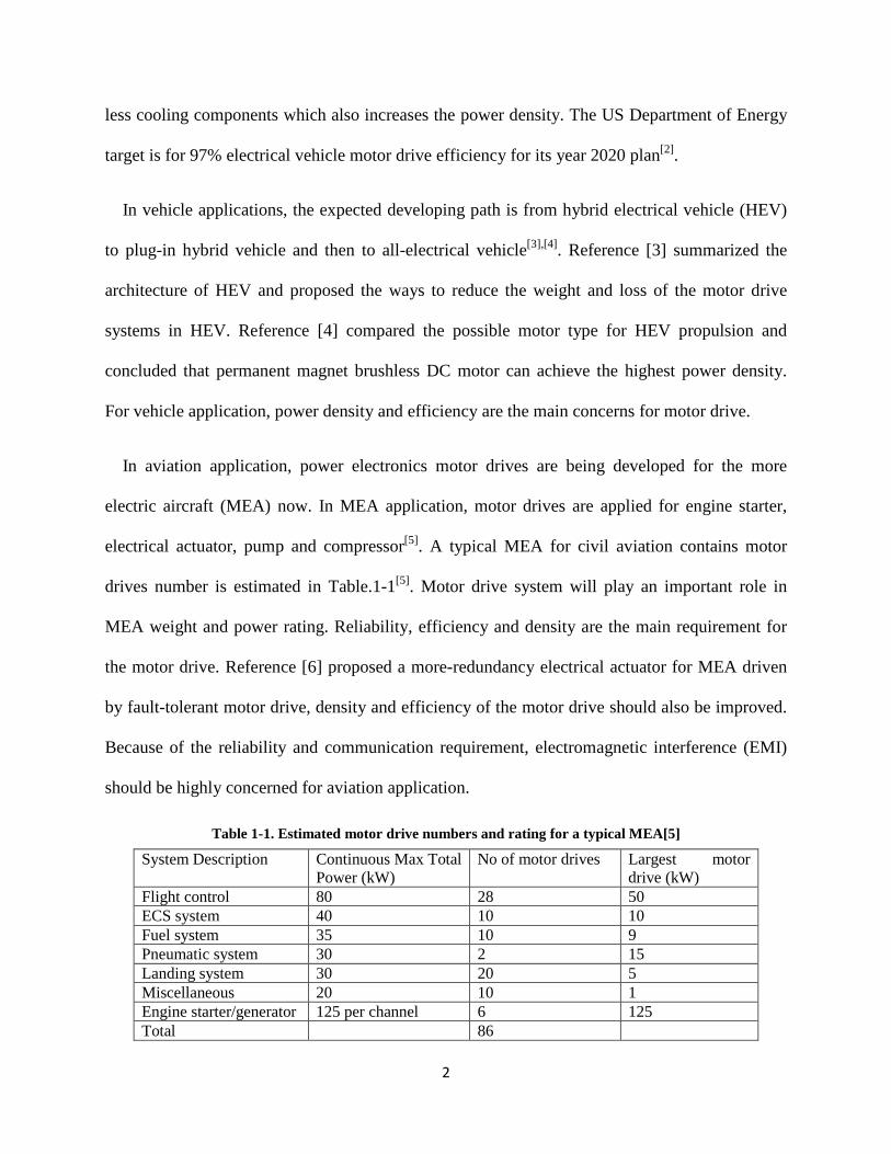
electric aircraft (MEA) now. In MEA application, motor drives are applied for engine starter,
electrical actuator, pump and compressor[5]. A typical MEA for civil aviation contains motor
drives number is estimated in Table.1-1[5]. Motor drive system will play an important role in
MEA weight and power rating. Reliability, efficiency and density are the main requirement for
the motor drive. Reference [6] proposed a more-redundancy electrical actuator for MEA driven
by fault-tolerant motor drive, density and efficiency of the motor drive should also be improved.
Because of the reliability and communication requirement, electromagnetic interference (EMI)
should be highly concerned for aviation application.
Table 1-1. Estimated motor drive numbers and rating for a typical MEA[5]
System Description Continuous Max Total Power (kW)
No of motor drives Largest motor drive (kW)
Flight control 80 28 50 ECS system 40 10 10 Fuel system 35 10 9 Pneumatic system 30 2 15 Landing system 30 20 5 Miscellaneous 20 10 1 Engine starter/generator 125 per channel 6 125 Total 86

3
In marine application, the concept of electrical war-ship is proposed by [7], including using
different kinds of motor drives for propulsion and actuation. Reference [8] and [9] summarized
the electrical motor drive architecture of the electrical ship propulsion.
For all these applications, the common problem is the power density, together with respective
performance requirements. This dissertation is studying the ways to improve motor drive power
density based on the specific requirement, including EMI, power quality and transient voltage.
Reference [10] summarized the power density barriers for most kinds of power electronics
converters and claimed that the maximum power density of 10kW/dm3 would be achieved in
around 2010. Reference [1] developed a 10kW AC-DC-AC converter with 2.8kg weight for
aircraft fan application, whose rated efficiency is 95.4%. Reference [11] discussed the efficiency
techniques for HEV system, pointing out that the switching loss of the power switches is the
main part to reduce.
Motor drive topology for the transportation system is an important factor to influence the
power density. Reference [12] introduced the possible topologies for motor drive. Reference [13]
systematically studied 4 typical AC-AC converter topologies for motor drive and concluded that
voltage source converters can achieve better density and efficiency comparing with current
source converters or matrix converters. In this dissertation, the main object is based on voltage
source converter type of motor drive.
More complex topologies could achieve better performance. Reference [14] studied the
application of multi-phase motor drive and [15] summarized the principle and application of
multi-level converter for motor drive. However, they require more devices and make the system
4
more complex. These topologies are more suitable for higher power application and will not be
studied in this dissertation.
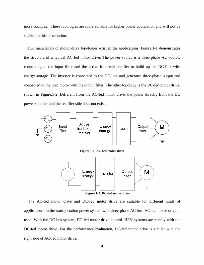
Two main kinds of motor drive topologies exist in the applications. Figure.1-1 demonstrates
the structure of a typical AC-fed motor drive. The power source is a three-phase AC source,
connecting to the input filter and the active front-end rectifier to build up the DC-link with
energy storage. The inverter is connected to the DC-link and generates three-phase output and
connected to the load motor with the output filter. The other topology is the DC-fed motor drive,
shown in Figure.1-2. Different from the AC-fed motor drive, the power directly from the DC
power supplier and the rectifier side does not exist.
Figure 1-1. AC-fed motor drive
Figure 1-2. DC-fed motor drive
The AC-fed motor drive and DC-fed motor drive are suitable for different kinds of
applications. In the transportation power system with three-phase AC bus, AC-fed motor drive is
used. With the DC bus system, DC-fed motor drive is used. HEV systems are mainly with the
DC-fed motor drive. For the performance evaluation, DC-fed motor drive is similar with the
right side of AC-fed motor drive.

5
For the AC source side of the AC-fed motor drive, the main concern of the system
performance is to reduce the harm to the AC source. Reference [16] introduced the power
quality standards for the grid connected converters, including the power factor, THD and EMI.
Reference [17] gave the aircraft AC power quality requirement for low order harmonics. For the
motor drives in the transportation system especially aircraft system, the conduction
electromagnet interference (EMI) is a very important performance standard since the conduction
EMI will impair the nearby equipments and reduce their reliability. Reference [19] defined the
aircraft EMI standard for Boeing 7E7 plane. Reference [20] systematically studied the conducted
EMI of active front-end rectifiers.
For inverter side of both AC-fed and DC-fed motor drive, the main concern of performance is
to reduce the harm to the motor. The power quality requirement is similar with the active front-
end side. Conduct EMI is harmful for motor especially the common-mode (CM) EMI current
which will be harmful for motor insulation. The current ripple of the inverter will brings torque
ripple for the motor and vibration and noise for the motor. The peak current ripple determines the
torque ripple peak value, and the THD of the current ripple determines the torque ripple average
effect. Reference [18] defined the harmonic distortion function (HDF) to evaluate the current
ripple’s effects.
For AC-fed motor drive, another performance requirement is the DC-link voltage variation[21].
The DC-link capacitor is usually determined by three factors. The first is system stability[13].
Figure.1-3 shows the system stability analysis based on impedance theory[22],[23]. With the
impedance margin of Zm and control bandwidth fBW, the DC link capacitor should satisfy (1-1).
The second requirement is the voltage switching ripple[13], with the maximum voltage ripple U∆
and the maximum output power Pmax, the DC-link capacitor should satisfy (1-2). The third and

6
the most critical requirement is the voltage peak in the transient, appears in load sudden change.
During the transient, before the rectifier fully response, some power will be supported by the
energy stored in DC link capacitor. Smaller DC-capacitor will have higher DC voltage peak or
sag, which will trigger the DC-link voltage protection. For the high density motor drive for the
fan-type of loads, this kind of transient is not considered and the DC-link capacitor is designed
based on (1-1) and (1-2).
Rectifier Inverter
outZinZ
C
Figure 1-3. DC-fed motor drive
mBWout
dc ZCfP
V ≥
−
π21
lg20lg202
(1-1)
swdc fUUV
PC
)2/( 2max
∆±∆≥
(1-2)
The power density should be pursued based on these requirements as constrains. Four typical
variables are studied in this dissertation: application of power electronic devices; passive
components; pulse width modulation (PWM) methods and motor control algorithms. Based on
the research background introduced in this section, this dissertation studies the methods of
pursuing high density and high efficiency for the motor drive with these four factors.
1.2 Current technical status
As discussed in 1.1, four factors are studies to pursue the high power density with satisfying
the performance constrains. This section summarizes the state-of-the-art of the techniques of the
four factors and their influence on motor drive power density. The unsolved problems of the

7
current techniques are also discussed. In order to implement the technique into motor drive, the
hardware status is also introduced.
1.2.1 Power electronics devices
The first factor is the application of power electronics devices. With fast switching devices,
the switching frequency of the motor drive can be higher and the passive filter could be reduced,
also the switching loss could reduce and the system efficiency will be higher, then the cooling
system volume and weight can also be reduced. What is more, the junction temperature of the
devices also contributes to the power density with reduction of cooling system.
Conventional silicon (Si) power devices have been pushed to their limits of the switching
speed and losses. Wide bandgap semiconductor devices are developed in the recent years
because of their better performance over the Si devices. Among the wide bandgap devices, the
silicon carbide (SiC) devices are the most widely applied wide bandgap power devices. Lower
loss is generally regarded as one of the most significant advantages of the SiC semiconductor
devices overt the conventional silicon (Si) devices. Another advantage of SiC semiconductor is
that it can perform well at higher temperature than Si devices, which can lead to smaller cooling
components.
At present, SiC Schottky barrier diode (SBD) and SiC JFET are among the main SiC switches
in the market. CREE and SiCED provide 1200V level SiC SBD and JFET which could be
applied for 10kW level motor drive. Many publications introduced method and results of SiC
device testing. Reference [24] proposed the method of testing SiC device switching with the
consideration of minimum measurement parasitic and can achieve 0Ω gate resistance switching.
[25] tested the SiC JFET under different temperatures up to 4000C. However, few of these tests

8
studied the SiC devices’ performance in real motor drive bridge and their influence on density
and efficiency.
Several demo motor drives with SiC devices were developed [26]-[30]. Center for Power
Electronics Systems (CPES) built up two versions of 10kW AC-fed motor drive with SiC JFETs
and SiC SBDs with non-regenerative three-level converter (NTC) and VSI structure which can
run with 70kHz switching frequency, the high temperature version converter is based on high
temperature package devices and could achieve smaller heatsink size. ETH in Zurich built a
2.5kW back-to-back (BTB) current source converter (CSC) with the similar devices and could
work with 200kHz switching frequency. Arkansas Power Electronics International (APEI) built
up a 4kW DC-fed motor drive with SiC JFET and SBD and claimed that it could be scaled-up to
100kW. The proto-type converter is with silicon on insulator (SOI) gate driver and can work at
high temperature. For higher power rating, a 55kW VSI based motor drive is introduced by the
Oak Ridge National Lab (ORNL) with Si IGBT and SiC SBD, claiming that the efficiency could
be obviously higher than all Si motor drive.
Table 1-2. Demo motor drives with SiC devices developed in recent years
Motor drive Rating Characteristics CPES 2008-2009[26],[27] 10kW, NTC+VSC SiC JFET+SBD, low temperature
and high temperature versions, fsw=70kHz
ETH 2008[28] 2.5kW BTB_CSC SiC JFET+SBD, fsw=200kHz APEI 2007[29] 4kW VSI SiC JFET+SBD, with SOI driver,
high temperature version ORNL 2006[30] 55kW VSI Si IGBT +SiC SBD
1.2.2 Passive components
Passive components in the motor drive could be divided into two main functions: one is the
component for switch assistant; the other is the passive filters.

9
In order to reduce the switching loss of the motor drive, the concept of resonant soft-switching
is introduced to motor drive with the resonant components. In [31], a 55kW soft-switching motor
drive is claimed to have efficiency higher than 98%. A zero current transition (ZCT) inverter is
introduced in [32] to achieve less switching loss. However, soft-switching inverter will highly
increase the complexity and reduce the reliability and currently is not preferred in most industrial
applications.
For passive component as filter, [33] systematically studied the impact of EMI filter on the
power density of three-phase PWM converters and proposed the design method for high density
EMI filter. Reference [34] proposed the EMI filter design with the conducted path. However, the
designed filter with inductor and capacitor are assumed to be with ideal value. Reference [35]
studied the parasitic and coupling issue of the passive filter component and the solutions for DC-
DC converter and this idea is introduced to three-phase converter in [36]. In real physical design
of the filter for motor drive, what kind of parasitic is the most important and how it influences
the density is a question which is very important for motor drive power density.
DC-link capacitor is another passive component influence the power density, as discussed in
1.1, stability, voltage ripple and transient peak determine the DC-link capacitor size. Reference
[37] studied the method of design a high density DC-link capacitor for PM motor drive.
1.2.3 Pulse width modulation (PWM) methods on density and efficiency
Different from the passive components’ influence, PWM methods are active methods to
improve the power density and efficiency of the motor drive. PWM methods highly influence the
switching loss and the current ripple, and determine the EMI sources.

10
Reference [38] summarized the methods for motor drive efficiency improvement and pointed
out that the device switching loss reduction is the most common way. Beside the soft-switching
discussed in 1.2.2, another idea is reducing the switching times. Reference [39] systematically
compared several kinds of PWM methods for three-phase converters and pointed out that the
main difference between space vector PWM (SVPWM), sinusoidal PWM (SPWM) and
discontinuous PWM (DPWM) is the arrangement of zero vectors, and they can achieve the same
line-to-line voltage. For phase voltage, the modulation signal of SVPWM and DPWM are the
modulation signal of SPWM plus a common-mode waveform, and could achieve higher
modulation index. With this principle, DPWM is preferred for reduction of switching loss since
one of the three phases is clamped to positive or negative bus and not switching in every
switching cycle. Reference [40] and [41] introduced the minimum-loss DPWM method which
reduced the switching loss with the biggest absolute current value.
PWM methods will influence the current ripple of the motor. Reference [42] and [43] studied
the current ripple caused by pulse sequence of SVPWM method and claimed that with different
voltage vector position, there is a optimized pulse sequence to achieve minimum current ripple
instead of using an unique pulse sequence. Then these papers proposed hybrid SVPWM method
to achieve minimum current ripple RMS value. Reference [44] derived the analytical expression
of current ripple of a single phase inverter and proposed a variable switching frequency PWM
method for the inverter which can adjust the switching frequency to adapt the current ripple
requirement. Then with the current ripple requirement, the optimized switching loss could be
achieved. However, for the more complex case of three-phase motor drive this method has not
been studied yet.

11
The main problem for current VSFPWM methods for three-phase PWM converter is lacking
theoretically analysis of current ripple and could not design the switching frequency variation
laws to arrange the current ripple. Reference [18] discussed the harmonic flux and Harmonic
Distortion Function (HDF) to evaluate the ripple current, but mainly studied the overall effect
but not ripple current distribution in time-domain. Reference [90] and [91] extended these
concepts to five-phase voltage-source converter and studied their influence on the Total
Harmonic Distortion (THD), but still not fully studied the current ripple distribution and variable
switching frequency.
PWM methods also determined the EMI noise source. With constant switching frequency the
power of EMI noise will converge in the integer harmonics of switching frequency. Then the
worst points to satisfy the EMI standard will also near the integer harmonics of switching
frequency. Random PWM (RPWM) is proposed by Trzynadlowski and other people[45]-[47] for
inverters. With randomly variable switching frequency the noise power will be spread in a wider
range and the noise peak will reduce. Experimental results have proved the reduction effects in
acoustic noise range by spectrum analysis of the inverter output current. However, for the higher
frequency range—EMI range, the effect of RPWM needs further study. Another issue for
RPWM is that there is not a quantified method to select the switching frequency, how to
determine the switching frequency is another question.
1.2.4 Motor control techniques
High performance AC machine feedback control technologies have been developed in the
recent years[48],[49] based on the AC machine mathematical models. The control object of the AC
motor is the electromagnetic torque of the machine then control the motor speed approach the

12
reference speed. These methods make the control of the complex AC machine similar with the
simple DC machine control and build up the basis of the adjustable AC motor drives.
There are two main methods for AC motor feedback control: vector control and direct torque
control (DTC). Vector control, or field orient control (FOC), is based on the AC machine d-q
model. By transferring the voltage and current into the rotating (d-q) frame, the AC value will be
converted to DC value and the torque is linearly depended on the d-q current and flux. DTC is
based on the stationary coordinate (D-Q) model. For different rotor position, each voltage vector
will affect respectively on the motor flux and torque. By selecting proper voltage vectors to keep
the motor flux and torque within tolerance with the reference value, the motor can also be
controlled well.
Another issue for motor control is sensing. In order to control the motor speed, rotor real speed
should be fed back. For coordinate transformation, rotor position is also required. Mechanical
position/speed sensor used for motor drive is expensive and reduces the system reliability. Based
on motor mathematical models, (position/speed) sensorless control is developed in the recent 30
years[48]. There are many sensorless control methods for AC motors, which could mainly divided
into two groups: methods based on fundamental wave model and based on harmonics model[50].
The methods based on harmonics model need extra high frequency signal to be injected into the
motor drive and extracted the rotor position and speed information from the harmonics, it could
achieve precise estimation results at low speed and stand still. The methods based on the
fundamental wave model do not need extra signal injection, but cannot get precise rotor position
and speed at low speed because of the small back-EMF.

13
The sensorless control methods based on fundamental wave model include linear observer,
model reference adaptive system (MRAS), extended Kalman filters (EKF), sliding mode
observer and so on. Mathematical model of the back-EMF observer based sensorless control
method of the permanent magnet synchronous motor (PMSM) is introduced by [51] and [52].
With this mathematical model, the observer bandwidth could be designed to meet the control
requirement.
For high density motor drive, because the passive components are designed to be small, how
will it influence the control method is an issue for the motor drive system.
1.2.5 Hardware status
Motor drive hardware usually contains two main parts: the power conversion main circuit and
the control system.
Reference [26] and [27] introduced a modular design method for high density motor drive.
The phase-leg of the motor drive (both for front-end rectifier and inverter) is build up in a phase-
leg module and all the modules are connected to the main board which contains the sensing and
protection functions. Then the motor drive could be developed based on modules and keeps the
interface between the module and the main board the same. In [26] and [27], high temperature
and low temperature versions of the phase-leg modules are connected to the same main board,
with interface of power paths and signal paths. Reference [54] introduced a high temperature
gate driver based on SOI structure, which could be used in the phase-leg module and push the
module temperature to be high.
Digital signal processor (DSP) plays an important role in motor drive control. The
development of DSP is from the fixed point DSP to the floating point DSP. Reference [55] did a

14
systematic comparison between fixed point DSP and floating point DSP in power electronics
control, claiming that the floating point DSP had better precision, higher dynamic range and less
quantization noise than fixed point DSP, and easier for coding. Texas Instrument (TI) is the main
supplier for power electronics control DSP. Its TMS320F2000 series DSP contains main
functions for motor drive control including AD channels and PWM channels[56]. Since 2007 it
has supplied the TMS320F28XXX series floating DSP for motor control application, which
makes the application of floating point DSP in motor drive much easier.
1.3 Research challenges and objectives
This dissertation aims at developing design and control techniques to achieve high power
density for the motor drive with satisfaction of the performance requirement. As discussed in 1.2,
there are many unsolved problems existing in the area. The system level explanation of how to
design and control high power density high efficiency motor drive with consideration of all of
the four aspects is studied in this dissertation. Four all the four aspects, there are many challenges:
(1) Device: although plenty of testing has been done for SiC devices and some are at high
temperature, the tests are based on single devices or with switch and diode commutation.
In real motor drive the devices are in the converter phase-leg, so the real performance of
SiC devices in the phase-leg is an unsolved problem. What is more, how will it influence
the power density and efficiency of the motor drive is another issue. Utilizing the
advantage of high temperature tolerance of SiC device, the cooling system can be
reduced, but how the device losses change at high temperature should be studied to
improve the efficiency of the motor drive.
(2) Passive: current physical designs of passive filter are mainly based on ideal model. Some
people studied the parasitic parameter’s influence on the passive filters and proposed

15
some solution. What parasitic parameters will highly influence the filter performance of
motor drives is another problem that needs to be solved.
(3) PWM: many works has been done on PWM methods used to influence the current ripple
and EMI of the motor drive. For ripple current attenuation, constant switching frequency
has its limits that it does not consider the ripple difference in different phase angles.
However, the analytical expression of the motor drive current is a complex problem, by
solving this problem the variable switching frequency PWM can be designed to achieve
less switching loss with the ripple requirement. Many works have been done on random
PWM to reduce the noise peak of motor drives. One of the challenges is how will
Random PWM improve the noise in EMI range and further improve the motor drive
density. Another function of improved PWM methods is the reduction of common-mode
noise. Although common-mode voltage peak value could be reduced by several improved
PWM methods, how it influences the common-mode noise current and common-mode
choke size are still unsolved problems.
Beside random PWM which is based on statistical effect, how to design more theoretical
variable switching frequency PWM to better utilize the freedom of switching frequency is
an important issue. To design switching frequency laws, the influence of PWM on
current ripple should be understood. The current ripple of three-phase motor drive is
influenced by the switching actions of every phase, and is more complex than single-
phase converter in reference [44]. Also, the current ripple requirement for three-phase
converter is also more complex than single-phase converter because it should consider all
the three phases. These issues make the variable switching frequency PWM for three-
phase PWM converter to be a hard problem.

16
(4) Control: plenty of high performance sensorless control methods could be used for motor
drive, however the motor low speed observing performance could not work well without
extra signal injection, so usually sensorless control should be started with non-sensorless
control. With high density design, the passive components are small and will be difficult
to tolerate the transient, how to adapt the motor control method to the high density motor
drive is an unsolved problem.
Based on these research challenges, main objectives of the research include the following four
parts:
(1) Devices: developing a precise measurement for SiC device in a phase-leg with high
temperature set-up. Analyzing the data for both conducting performance and switching
performance and developing loss models. Then the influence of temperature on the
density and efficiency of motor drives with SiC devices could be concluded.
(2) Passive: With the physical designed EMI filter, the coupling parasitic parameters’
influence on EMI noise attenuation is going to be studied.
(3) PWM method: Two main areas with PWM are studied for high power density motor
drives.
First, PWM methods’ influence on inverter CM noise is also going to be studied. The
goal is to reduce the CM noise current and minimize the CM choke size.
Another area for PWM is to analyze and design variable switching frequency PWM
methods for three-phase converters. Beside Random PWM method for active front-end
rectifier to improve EMI, the analytical current ripple expressions are studied at first as
the basis for variable switching frequency PWM method. Then based on different kinds
of current ripple requirements, variable switching frequency PWM methods are

17
developed to arrange the current ripple and achieve loss and EMI reduction for the
converter.
(4) Motor control: developing a sensorless control method for PMSM with high density
motor drive to achieve less transient peak in start-up process.
AC-fed motor drive experiments are done in the high density motor drive developed in [26]
and [27]. Developing a DC-fed motor drives hardware structure is the hardware object of this
dissertation.
1.4 Organization of the dissertation
The dissertation presents a systematic methodology for design and control of high power
density high efficiency motor drive. The chapters are organized as follows:
Chapter 2 studies the performance of SiC devices for motor drive. First, the physical
characteristic and application of SiC devices is introduced. Then the conducting performance of
the SiC JFET (with and without external SiC SBD) is evaluated. Switching performance of SiC
devices in a phase-leg is evaluated in a double-pulse-test (DBT) board with high temperature set-
up. Then the device losses model is proposed and the whole motor drive losses is estimated and
compared.
Chapter 3 studies the EMI attenuation methods for the active front-end rectifier of motor
drives. The EMI problem is introduced at first, and then the basic design of EMI filter is
discussed. With the basic design, the parasitic coupling issue is studied. Then the analysis and
experiments of Random PWM for EMI attenuation is introduced. Conclusion is made in the end
of this chapter.

18
Chapter 4 introduces the research of PWM methods’ influence on common-mode noise
reduction. Different PWM methods are compared as common-mode noise sources. Comparing
with conventional SVPWM and DPWM, two improved PWM methods could achieve less CM
voltage peak. The CM voltage source analysis, CM current analysis and CM choke volt-seconds
problems are presented to study the impact of PWM methods on the CM noises. Experiments are
presented to support the study and the conclusions are made in the end of this chapter.
Chapter 5 studies the variable switching frequency PWM methods for three-phase PWM
converters. First, analytical current ripple expressions are studied for both SVPWM and DPWM,
and verified by simulation and experimental results. The architecture of variable switching
frequency PWM is proposed based on ripple current prediction. Then based on two kinds of
ripple requirement: peak ripple current requirement and RMS ripple current requirement, two
kinds of variable switching frequency PWM methods are proposed as VSFPWM1 and
VSFPWM2 to improve losses and EMI noises, and verified with experimental results.
Conclusions are made in the end of this chapter.
Chapter 6 studies the PM motor control techniques for high density motor drive. Back-EMF
observer based sensorless vector control for PM motor is introduced first. Then the improved
start-up method is proposed to achieve small transient peak of DC-link voltage. With this start-
up method, the motor control experimental results are presented and the conclusions are made in
the end of this chapter.
Chapter 7 presents the hardware design and development of a high density high efficiency
motor drive as the hardware design example. After brief introduction, the system configuration

19
and interface is introduced at first. Then the hardware design and construction of the motor drive
is introduced. The designed motor drive test results are presented in the end of this chapter.
Finally Chapter 8 summaries the conclusions for the technologies developed in this
dissertation, and discuss the continuous work for design and control for high power density
motor drives.

20
Chapter 2. SiC Devices Analysis in Motor Drive
This chapter mainly studies the performance of SiC devices applied in motor drives especially
their influence on motor drive losses. This chapter starts with an introduction to the basic
knowledge and the-state-of –the-art of SiC devices. Then the conduction performance evaluation
of SiC devices is introduced in 2.2. A testbed of SiC devices phase-leg switching is introduced in
2.3 together with the switching waveform at different temperatures. With the performance
evaluation, the device conduction and switching loss model is introduced in 2.4, and then the
converter loss is estimated. Conclusions are made in 2.5.
2.1 Introduction of SiC devices
Advanced power electronics semiconductor techniques are usually propulsion for motor drive
power density and efficiency. The development of conventional silicon (Si) power devices is
approaching to their limits. Recent years with the development of wide bandgap power devices,
their application in motor drives are also studied [26]-[30]. Among the wide bandgap devices,
silicon carbide (SiC) devices are the most popular kinds of devices for power conversion
application now.
Lower loss is generally regarded as one of the most significant advantages of the emerging
SiC semiconductor devices overt the conventional Si devices. Another advantage of SiC
semiconductor is that it can perform well at higher temperature than Si devices. For motor drive
application, with the devices performing well at high temperature, the cooling system volume
can be effectively reduced.

21
There have been considerable previous works on SiC devices characterization and loss
modeling. [57]-[64]. However, most of the SiC characterization and loss modeling have been based
on single device. On the other hand, in high power applications where SiC devices can make the
greatest impact, they are most often used in a phase-leg topology. This chapter focuses on the
characterization of SiC device in a phase-leg configuration especially in high temperature. The
results and methodology will provide useful and practical tool in SiC converter design.
At present, SiC Schottky diode and SiC JFET are the main SiC switches. Most of the
researches deal with low current (less than 5A) low power cases (less than 2kW). CREE provides
1200V, 10A SiC Schottky diode C2D10120 in the market and SiCED can provide 1200V, 20A
SiC normally-on JFET with 4.18mm*4.18mm die size. 10kW, 600V level motor drive can be
made with these kinds of devices which can work at 200 0C high temperature. In this chapter,
these two devices are used as the switches.
Figure.2-1 shows the typical structure of SiC Schottky diode. In fabrication, a suitable metal is
evaporated onto the n-n+ epitaxial structure, forming Schottky barrier. With this structure,
charge transportation in the diode is by majority carriers therefore has little reverse recovery.
Figure.2-2 shows the structure of a SiC JFET with a channel in the n- drift region[61], if no gate
voltage is added between gate and source, current can conduct in both drain-to-source and
source-to-drain directions, but if enough negative voltage is added between gate and source, the
channel will be blocked. However, in Figure.2-2, a normal P-N junction exists in the JFET which
can be treated as a body diode. Because it does not contain the Schottky barrier, it has reverse
recovery phenomenon. In a SiC voltage source converter phase-leg, the JFET body diode can be
used as the anti-paralleling diode without using extra freewheeling diode[61]. However, with and
without Schottky diode as anti-paralleling diode, both conduction and switching performance of

22
the converter will be different. Reference [62] and [63] compared the reverse recovery
performance of SiC Schottky diode and normal diode, but did not study the body diode.
Reference [61] studied the switching performance difference between body diode of JFET and
Schottky diode at different temperature and concluded that with Schottky diode as anti-
paralleling diode the switching performance can be improved. This chapter presents a
comprehensive evaluation of SiC JFET and diode loss in a converter phase-leg with
consideration of temperature.
Figure 2-1. Structure of SiC Schottky diode
Figure 2-2. Structure of SiC JFET
Three-phase voltage source converter (VSC) total power losses depend on the device
conduction losses and switching losses. Reference [40] and [41] studied the method of
calculating total losses of three-phase VSC using IGBT type devices. The loss model is different

23
in the VSC with JFET. What is more, the temperature’s influence has not been extended to
higher than 1250C, which has more serious penalties. Reference [58]-[60] studied three-phase
converter losses based on SiC FET devices with anti-parallel diode, using switching losses based
on switch-to-diode switching test results, which is different from switch-to-switch (either with
diode or without diode) switching loss in the real VSC. Reference [57] and [61] studied the
switching performance based on switch-to-switch switching test, but did not study the switching
losses in this case. For conduction losses, most papers treat the conduction resistance of the
switch to be constant at the same temperature; however, with different conduction direction
conduction resistance difference should be noticed. [28] studies the loss of back-to-back current
source converter (CSC) with SiC JFET and diode, but the switching and conduction loss are
difference from VSC. All these considerations make that the total losses calculation of SiC JFET
converter need to be developed in a new way.
This chapter studies the performance evaluation and loss calculation method of SiC JFET in a
voltage source converter considering the temperature’s influence, especially compares the
performance and loss for the converter with and without SiC Schottky diode as anti-paralleling
diode. In 2.2, the conducting performance and conduction loss of the device is evaluated
considering drain-to-source and source-to-drain differences and the influence of anti-paralleling
diode in a wide temperature range. In 2.3, a testbed of converter phase-leg considering
temperature’s influence has been built and the switching performance for the converter phase-leg
(both with and without SiC Schottky diode as freewheeling diode) has been studied. In 2.4, based
on the switching waveform the switching loss model is developed, and then total power loss is
calculated in a 10kW bidirectional AC-DC-AC converter. Comparison is made to study the
influence factors on the total loss. Conclusions are made in 2.5.

24
2.2 SiC devices conduction performance evaluation
As discussed in the introduction, conduction losses calculation methods in most paper treat the
switch as a constant on-state resistance when conducting. However, based on the structure of
JFET in Figure.2-2, positive direction (drain-to-source) and negative direction (source-to-drain)
conducting current do not have identical path. Measured static conduction characteristics results
are shown in Figure.2-3. The V-I curves are linear in both direction, proving that in both
direction JFET can be treat as resistor. By calculating the slop of each V-I curve, the equivalent
resistance of JFET can be estimated, as shown in Figure.2-4. Rds and Rsd indicate the drain-to-
source and source-to-drain equivalent resistance respectively. The difference between resistances
in two directions increases as the temperature increases. In the converter loss calculation, current
direction in the device should be determined and with different current direction, different Rds
and Rsd should be used.
0 1000 2000 3000 40000
2
4
6
8
10
12
14
16
18
Vds / mV
Id /
A
D-S Characteristic
0 1000 2000 30000
2
4
6
8
10
12
14
16
18
Vsd / mV
Id /
A
S-D Characteristic
Figure 2-3. SiC JFET conduction performance in D-S (left) and S-D (right) direction from 250C-2000C
25
20 40 60 80 100 120 140 160 180 20080
100
120
140
160
180
200
220
Rds
Rsd
Figure 2-4. JFET conduction resistance in two directions
The SiC Schottky diode conduction characteristics at different temperatures are measured and
shown in Figure.2-5, they can be modeled with a temperature-dependent voltage source Von and
resistance Rd. Rd will increase with higher temperature but Von will decrease with higher
temperature.
0 500 1000 1500 2000 2500 3000 3500 40000
5
10
15
20
Vd / mV
Id /
A
250C
1000C
2000C
Figure 2-5. SiC Schottky diode (C2D10120) conduction characteristics
Therefore, the JFET conduction loss can be appropriately characterized by Rds in the drain-to-
source direction and Rsd in the source-to-drain direction, if the switch does not have extra anti-
paralleling diode, it can be treated as Rsd, but with freewheeling diode, the source-to-drain
direction circuit model is made up with Rsd in parallel with the external diode, shown in
Figure.2-6. If the current is less than the threshold value, the diode is not conducting and the
current only goes through Rsd, if the current is larger than the threshold value, current will go in
26
both Rsd and the diode. The distribution of current in this case is shown in (2-1). From (2-1) the
voltage drop and conduction loss in the switch can be calculated in (2-2). The conduction loss
power of JFET in different cases can be summarized in Table.2-1.
dR
sdR
onVI
1I
2I
Figure 2-6. S-D conduction model of JFET with freewheeling diode
=+=+
III
RIVRI sdond
21
21 (2-1)
++=
++=
sdd
sddsdon
sdd
sddsdon
RR
RRIIRVP
RR
RIRRVV
2 (2-2)
Table 2-1. Conduction loss power of JFET
Without freewheeling diode With freewheeling diode
D-S direction dsRI 2 dsRI 2
S-D direction sdRI 2
>++
=
≤=
sd
on
sdd
sddsdon
sd
onsd
R
VI
RR
RRIIRVP
R
VIRIP
2
2
2.3 SiC devices switching performance evaluation
Switching loss of SiC JFET is evaluated by double-pulse test (DBT). Several considering are
required for the design of double-pulse testbed for SiC JFET, including the circuit layout and
measurement to achieve the precise switching waveform with minimum influence from the
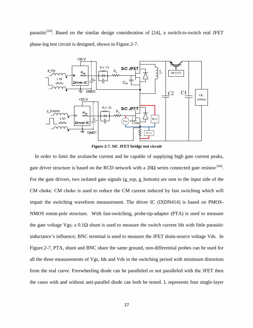
27
parasitic[24]. Based on the similar design consideration of [24], a switch-to-switch real JFET
phase-leg test circuit is designed, shown in Figure.2-7.
Figure 2-7. SiC JFET bridge test circuit
In order to limit the avalanche current and be capable of supplying high gate current peaks,
gate driver structure is based on the RCD network with a 20Ω series connected gate resistor [64].
For the gate drivers, two isolated gate signals (g_top, g_bottom) are sent to the input side of the
CM choke. CM choke is used to reduce the CM current induced by fast switching which will
impair the switching waveform measurement. The driver IC (IXDN414) is based on PMOS-
NMOS totem-pole structure. With fast-switching, probe-tip-adapter (PTA) is used to measure
the gate voltage Vgs; a 0.1Ω shunt is used to measure the switch current Ids with little parasitic
inductance’s influence; BNC terminal is used to measure the JFET drain-source voltage Vds. In
Figure.2-7, PTA, shunt and BNC share the same ground, non-differential probes can be used for
all the three measurements of Vgs, Ids and Vds in the switching period with minimum distortion
from the real curve. Freewheeling diode can be paralleled or not paralleled with the JFET then
the cases with and without anti-parallel diode can both be tested. L represents four single-layer

28
24-turn 250 µH inductors used for the DBT to achieve low equivalent parasitic capacitance
(EPC).
For phase-leg test, shoot-through protection needs to be considered, especially for the phase-
leg with normally-on JFETs. The shoot-through protection of the circuit is realized by an IGBT
driven by a current-sensing single-channel drive (IR2127), shown in Figure.2-7. C1 is a 2*2
bank of 450V-800µF aluminum electrolytic capacitor (AEC), which can serve as bulk capacitor
for supplying high current. C2 is an array of 1kV 250nF film capacitors which are located close
to the devices, providing a high frequency decoupling layers from the remaining dc bus stray
inductance. With C2, the waveform of switching voltage could be clean and the EMI problem
can be reduced. Parasitic inductance in the switching loop will cause oscillation and over-
shooting in the turn-off voltage. The PCB layout principle for parasitic minimization can reduce
the influence of oscillation problem, discussed in [24]. C2 stores little energy (less than 0.4J with
600V dc bus voltage). When the shoot-through happens, IGBT will be turned off and isolating
the DC source and the bulk AECs from the bridge, the circuit is protected.
In order to test the switching performance in high temperature, a high-temperature test set-up
is shown in Figure.2-8. The device is heated by connecting to a controlled hot plate on the
bottom side of test board, in order to make sure the gate driver and shunt are not heated to high
temperature, a fan is used to cool them and thermal couples are used to monitor the temperature.
Thermal isolation is also made for the shunt to make sure the shunt resistance will not be
influenced much by the heating. This set-up is simple and can simulate the similar situation for
high temperature inside the device but normal temperature in the circuit.
The actual testbed for high temperature switching experiments is shown in Figure.2-9. SiC
JFET based switching bridge with measurement devices are integrated in the PCB.

29
PCB
Device
Copper
connector Hot plate
Shunt
Gate driver
Thermal
couple 1, 2
Thermal
couple 3
Thermal
couple 4
Thermal
isolation
Fan
Thermal
controller
Figure 2-8. High temperature experimental set-up of switching test
Figure 2-9. Actual testbed for high temperature switching experiments
With the high temperature switching testbed, switching performance of the JFET has been
done at 250C, 1000C and 2000C, with 600V bus voltage and 5A,7A,9A,11A,13A and 15A
inductor current, both for with and without anti-paralleling diode, results are shown in Fig.2-10.
In order to make a comparison with non-bridge switching result, results of JFET switching with
SiC Schottky diode are also displayed in Figure.2-10.
Figure.2-10(a) shows the turn-on waveform of JFET-to-JFET switching without extra anti-
paralleling diode with 15A current at 250C, 1000C and 2000C. The current overshoot is much
worse at 2000C than at 250C. The switching energy in high temperature is also obviously bigger
than in low temperature. Figure.2-10 (d) shows the turn-off waveform of JFET-to-JFET

30
switching without extra anti-paralleling diode with 15A current at 250C, 1000C and 2000C. With
higher temperature, turn-off time of JFET is less, the turn-off time at 2000C is about 50ns less
than that of 250C, so the turn-off loss of JFET will decrease with temperature rising.
Figure.2-10(b) shows the turn-on waveform of JFET-to-JFET switching with external anti-
paralleling diode with 15A current in 250C, 1000C and 2000C. With SiC Schottky diode as anti-
paralleling diode, in the dead time most of the current will go through the freewheeling diode
and this part of current will have no reverse recovery, only the current which is still going
through the body diode has reverse recovery phenomenon. Figure.2-10 (b) shows that the turn-on
overshoot current is much less than the case without external diode especially in high
temperature (Figure.2-10(a)). For 2000C case, the turn-on current overshoot for Figure.2-10(b) is
about 8A, but in Figure.2-10(a), the turn-on current over-shoot is more than 16A, about twice as
Figure.2-10(b). That means the turn-on loss of JFET will be less than the case without
freewheeling diode. Figure.2-10 (e) shows the turn-off waveform of JFET-JFET switching with
external diode in 250C, 1000C and 2000C. Similar with Figure.2-10(d), the turn-off time
decreases as the temperature rises.
To make a comparison, the turn-on waveform of JFET switching with only SiC Schottky
diode is shown in Figure.2-10 (c). There is no obvious overshooting current in either high or low
temperature because of no reverse recovery. The switching loss using this test result will be less
than the real case in voltage source converter with bridges. Figure.2-10 (f) is the turn-off
waveform of this case.

31
50 100 150 200 250 300 3500
10
20
30
40Id
/ A
50 100 150 200 250 300 350-200
0
200
400
600
800
time / ns
Vd
s / V
(a)
50 100 150 200 250 300 350
0
5
10
15
20
Id /
A
50 100 150 200 250 300 350-200
0
200
400
600
800
time / ns
Vd
s / V
(d)
50 100 150 200 250 300 350
0
5
10
15
20
25
Id /
A
50 100 150 200 250 300 350-200
0
200
400
600
800
time / ns
Vd
s / V
(b)
50 100 150 200 250 300 350
0
5
10
15
20
Id /
A
50 100 150 200 250 300 350-200
0
200
400
600
800
time / ns
Vd
s / V
250C
1000C
2000C
250C
1000C
2000C
(e)
-50 0 50 100 150
0
5
10
15
20
Id /
A
-50 0 50 100 150-200
0
200
400
600
800
time / ns
Vd
s / V
(c)
-50 0 50 100 150 200
0
5
10
15
20
Id /
A
-50 0 50 100 150 200-200
0
200
400
600
800
time / ns
Vd
s / V
(f)
Figure 2-10. Switching waveform of JFET bridge (a) JFET turning on only with JFET (b) JFET turning on with both JFET and diode (c) JFET turning on only with diode (d) JFET
turning off only with JFET (e) JFET turning off wit h both JFET and diode (f) JFET turning off only with diode

32
For SiC JFET in a phase-leg, the turn-on waveform is related to the diode of the
complementary switch. This diode could be the body diode of the complementary JFET (in the
case of diode-less bridge) or the body diode paralleling with an extra SiC Schottky diode. The
body diode of JFET has bad reverse recovery performance especially at high temperature, which
causes big over-shooting in the JFET turn-on waveform (Figure.2-10(a)). Paralleling with
external SiC Schottky diode, this over-shooting will be obviously improved (Figure.2-10 (b)) but
the body diode still influence the over-shooting and the waveform is worse than the case with
only SiC Schottky diode (Figure.2-10 (c)).
For the turn-off waveforms of the three cases, the phenomenon is similar. With rising
temperature, the turn-off time will reduce. This is an advantage for high temperature application
which reduces the turn-off losses.
If further increase the switching speed by decreasing the gate resistor, the over-shooting of the
turn-on current will be even higher and make it unacceptable. The switching waveforms of the
bridge without external SiC Schottky diode as anti-paralleling diode but with only 10Ω gate
resistor at 2000C are shown in Figure.2-11(a). For the turn-on waveform, the current over-
shooting is up to 45A (with 15A steady state current), that will not only bring bigger switching
loss, but also bring worse EMI problem for the converter system. Comparing Figure.2-11(a) and
Figure.2-10(a), 100% more over-shooting current appears in the smaller gate driver resistance
case. Comparing Figure.2-11(b) and Figure.2-10(d), with smaller gate resistance, 60ns turn-off
time can be achieved comparing with 90ns turn-off time of bigger gate resistance case. But
considering of the penalty of the turn-on overshooting, decreasing gate resistance should not be
preferred in the case of the bridge without SiC Schottky diode.

33
50 100 150 200 250 300 3500
10
20
30
40
50
Id /
A
50 100 150 200 250 300 350-200
0
200
400
600
800
time / ns
Vd
s / V
250C
1000C
2000C
250C
1000C
2000C
50 100 150 200 250 300
0
5
10
15
20
Id /
A
50 100 150 200 250 300-200
0
200
400
600
800
time / ns
Vd
s / V
(a) (b)
Figure 2-11. Turn-on (a) and turn-off (b) waveform in the bridge with only JFET at 250C, 1000C,2000C: With 10 Ω gate resistance
When SiC Schottky diode is paralleled with the JFET in the bridge, decreasing the gate
resistance to 10Ω, the switching performance is shown in Figure.2-12, with 2000C ambient
temperature. The over-shooting problem could be improved. In Figure.2-12(a), the overshooting
peak is 12A above the steady state, about 50% higher than the case of Figure.2-10(b). The turn-
on time is about 80ns and the turn-off time is about 60ns. Comparing with the case without SiC
Schottky diode, decreasing the gate resistance can effectively accelerate the switching without
obviously deteriorated over-shooting.
Comparing with Figure.2-10(b), the fast gate driver does not cause obvious overshooting
change in the whole temperature range because of the tolerance of the SiC Schottky diode
against the temperature. The total commutation period of turn-on is 80ns and turn-off is 60ns at
2000C, comparing with 100ns (Figure.2-10(b)) and 90ns (Figure.2-10 (e)) with 20 Ω gate
resistance, the phase-leg with freewheeling diode can actually increase the switching speed
without obvious penalty. Similar with the previous cases, the turn-off waveform does not change
much and the turn-off time decreases as the temperature rises.

34
50 100 150 200 250 3000
10
20
30Id
/ A
50 100 150 200 250 300-200
0
200
400
600
800
time / ns
Vd
s / V
(a)
50 100 150 200 250 300
0
5
10
15
20
Id /
A
50 100 150 200 250 300-200
0
200
400
600
800
time / ns
Vd
s / V
(b)
Figure 2-12. Turn-on (a) and turn-off (b) waveform in the bridge with paralleled SiC Schottky diodes at 250C, 1000C,2000C: With 10 Ω gate resistance
2.4 Device and converter loss estimation
The motor drive losses include the conduction losses and switching losses. The device
conduction losses are evaluated in Table.2-1. The switching losses of the devices in the phase-leg
are evaluated with the switching waveform.
In order to estimate the switching loss of one phase-leg of SiC JFET, the switching process is
analyzed in Figure. 2-13. The commutation is realized in the dead time. In every switching time,
one of the switches is actively switched by the gate signal, and the other switch is forced to turn
on or turn off with the freewheeling diode.
The switching Figure.2-13 (a) defines the voltage and current in the top and bottom switch in
one phase leg. Without lose of generality, define the load current I load direction toward the
middle point of the bridge. (Actually when current is in the in the opposite direction the
switching loss in the phase leg will not be changed; only distribution is inversed between the two
switches). Because of the DC link capacitor and the load inductor, (2-3) is realized.

35
=+=−
dc
load
VVV
III
21
21
(2-3)
With (2-3) and the experimental results, general voltage and current waveforms of the two
switches are shown in Figure.2-13(b) and Figure.2-13(c). For the case of bottom switch turn-on,
shown in Figure.2-13(b), before time t0, current I2 is -Iload and it will change synchronously with
I1. Between time t1 and t3 the reverse recovery area in S2 will cause an extra loss in the top switch.
For the case of bottom switch turn-off, shown in Figure.2-13(c), beside the overlap area of S1
(t4~t6) will cause switching loss in the bottom switch, there is also an overlap area in the top
switch S2 (t4~t5), the product of I2 and V2 is negative, means that energy is generated but not
consumed. In physical analysis, the released energy is stored in the junction capacitor of the
freewheeling diode of S2 in the turn-on process of S1. This part of the energy loss is not
consumed in the turn-on process of S1, so it should be subtracted in the total switching energy
loss.
t0 t1 t2 t3
I1
I2
V2
V1
Vdc
Vdc
Iload
-Iload
0
0
0
0
(a) (b) (c)
Figure 2-13. Voltage/current definition in phase-leg (a) and general switching waveforms for switch 1 turn-on (b) and turn-off (c)
The switching energy loss of one turn-on and turn-off action in the single bridge can be
calculated as the sum of three parts:
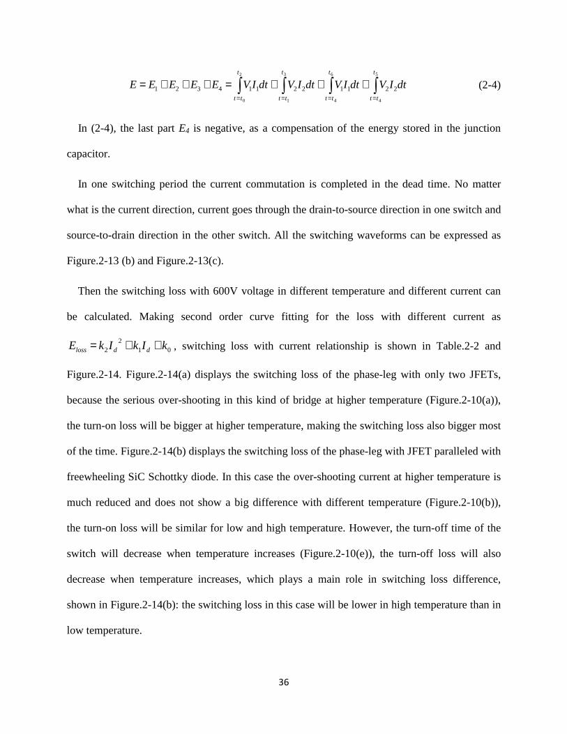
36
∫∫∫∫====
+++=+++=5
4
6
4
3
1
2
0
221122114321
t
tt
t
tt
t
tt
t
tt
dtIVdtIVdtIVdtIVEEEEE (2-4)
In (2-4), the last part E4 is negative, as a compensation of the energy stored in the junction
capacitor.
In one switching period the current commutation is completed in the dead time. No matter
what is the current direction, current goes through the drain-to-source direction in one switch and
source-to-drain direction in the other switch. All the switching waveforms can be expressed as
Figure.2-13 (b) and Figure.2-13(c).
Then the switching loss with 600V voltage in different temperature and different current can
be calculated. Making second order curve fitting for the loss with different current as
012
2 kIkIkE ddloss ++= , switching loss with current relationship is shown in Table.2-2 and
Figure.2-14. Figure.2-14(a) displays the switching loss of the phase-leg with only two JFETs,
because the serious over-shooting in this kind of bridge at higher temperature (Figure.2-10(a)),
the turn-on loss will be bigger at higher temperature, making the switching loss also bigger most
of the time. Figure.2-14(b) displays the switching loss of the phase-leg with JFET paralleled with
freewheeling SiC Schottky diode. In this case the over-shooting current at higher temperature is
much reduced and does not show a big difference with different temperature (Figure.2-10(b)),
the turn-on loss will be similar for low and high temperature. However, the turn-off time of the
switch will decrease when temperature increases (Figure.2-10(e)), the turn-off loss will also
decrease when temperature increases, which plays a main role in switching loss difference,
shown in Figure.2-14(b): the switching loss in this case will be lower in high temperature than in
low temperature.

37
Table 2-2. Switching loss with 600V voltage
Switching loss (µJ) Switching loss (µJ) 250C, with only JFET
0.984Id2+41.5Id+187 2000C, with only
JFET 1.703Id
2+74.9Id+37
250C, with JFET & diode
0.700Id2+39.2Id+148 2000C, with JFET &
diode 1.617Id
2+16.3Id+169
The comparison in Figure.2-14 shows that when using the SiC JFET converter without using
the external SiC Schottky diodes, the switching loss at high temperature will much worse than at
low temperature, reduction of the switching frequency at high temperature may be required.
However, the switching loss for the converter with SiC Schottky diode as anti-paralleling diode,
the switching loss at high temperature will be even less than in low temperature, this
phenomenon implies that the converter using external SiC Schottky diode can achieve much
better performance in high temperature than without using external SiC Schottky diode.
4 6 8 10 12 14 16200
400
600
800
1000
1200
1400
1600
1800
Id / A
Lo
ss /
uJ
(a)
4 6 8 10 12 14 16200
400
600
800
1000
1200
1400
1600
1800
Id / A
Lo
ss /
uJ
250C
2000C
(b)
Figure 2-14. Switching loss linearization (a) JFET switching only with JFET (b) JFET switching with both JFET and diode
Base on the analysis results, the total loss of a three-phase converter can be determined. In this
chapter, a 10kW AC-DC-AC voltage source converter is considered. Its rated values are shown
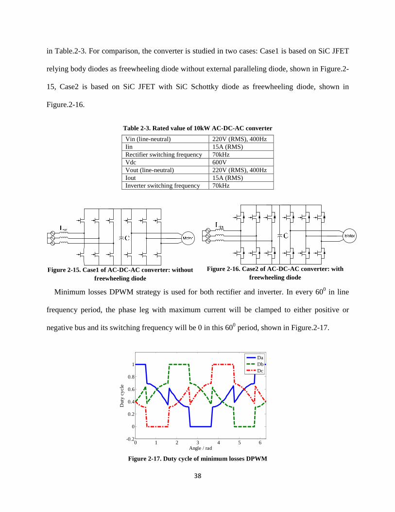
38
in Table.2-3. For comparison, the converter is studied in two cases: Case1 is based on SiC JFET
relying body diodes as freewheeling diode without external paralleling diode, shown in Figure.2-
15, Case2 is based on SiC JFET with SiC Schottky diode as freewheeling diode, shown in
Figure.2-16.
Table 2-3. Rated value of 10kW AC-DC-AC converter
Vin (line-neutral) 220V (RMS), 400Hz Iin 15A (RMS) Rectifier switching frequency 70kHz Vdc 600V Vout (line-neutral) 220V (RMS), 400Hz Iout 15A (RMS) Inverter switching frequency 70kHz
Figure 2-15. Case1 of AC-DC-AC converter: without freewheeling diode
Figure 2-16. Case2 of AC-DC-AC converter: with freewheeling diode
Minimum losses DPWM strategy is used for both rectifier and inverter. In every 600 in line
frequency period, the phase leg with maximum current will be clamped to either positive or
negative bus and its switching frequency will be 0 in this 600 period, shown in Figure.2-17.
Figure 2-17. Duty cycle of minimum losses DPWM
0 1 2 3 4 5 6-0.2
0
0.2
0.4
0.6
0.8
1
Angle / rad
Dut
y cy
cle
DaDbDc

39
Dividing one line period T0 into N switching period with width of Ts. Calculating the
conduction energy loss Econ of three-phase converter based on (2-5), the conduction power
Pconx(n) is determined by the current direction and calculated by Table.1. The switching energy
loss Esw is calculated by (2-6). In (2-6), if the duty cycle is 0 or 1, the phase leg is clamped and
the switching loss Esw,x is 0, if duty cycle is neither 0 nor 1, the switching loss Esw,x is calculated
by Table.3. Then the total switching energy loss of the three phase converter in one line-cycle is
calculated by (2-7), the power loss is calculated by (2-8).
∑ ∑= =
=cbax
N
nsxconxcon TndnPE
,, 1
)()( (2-5)
=
<<++=
1,0)(0
1)(0600
))()(()( 01
2
2,
nd
ndV
knIknIknE
x
xdc
xxxsw (2-6)
∑ ∑= =
=cbax
N
nxswsw nEE
,, 1, )( (2-7)
00 //__ TETEcPsPP consw +=+= (2-8)
Inverter and rectifier conduction losses with Case1 and Case2 at 250C and 2000C are shown in
Figure.2-18. At full power full voltage, the difference caused by the anti-paralleling diode in
inverter conduction loss is not obvious because most current is in JFET (drain to source
direction), but the difference is obvious in rectifier because current is mainly in the source to
drain direction and distributed between JFET channel, body diode and Schottky diode if there is
one. Inverter and rectifier switching loss with Case1 and Case2 at 250C and 2000C are shown in
Figure.2-19. Because of the reverse recovery caused by body diode, Case1 has higher switching
loss. The difference is much more pronounced at 2000C.
Figure.2-20 shows the comparison of the total converter losses between Case1 and Case2 at
250C and 2000C. With external SiC Schottky as anti-paralleling diode (Case2), because both the

40
conduction and switching loss of the switch will be less than the case without SiC Schottky diode
as freewheeling diode, both the rectifier and inverter total losses will decrease. This difference is
more obvious at high temperature.
The total loss distribution in the motor drive of Case1 and Case2 are shown in Figure.2-21,
both at 2000C. For case1 (without SiC Schottky diode as freewheeling diode), inverter
conduction loss is not dominated. If the SiC Schottky diode is added, the conduction loss of the
inverter does not change much in value because the current in the inverter mainly goes through
drain-to-source direction, but the other 3 kinds of losses will obviously reduce because of the
benefit of the freewheeling SiC Schottky diode. This causes the conduction loss of the inverter to
be the biggest in case 2. The total loss of the back-to-back converter will decrease from 537W in
case 1 to 365W in case 2, increasing the efficiency from 94.6% to 96.3% with the rated load.
Figure 2-18. Converter conduction losses at 250C (left) and 2000C (right)
Figure 2-19. Converter switching losses at 250C (left) and 2000C (right)
0
20
40
60
80
Inverter Rectifier
Case1
Case2
0
50
100
150
Inverter Rectifier
Case1
Case2
0
50
100
Inverter Rectifier
Case1
Case2
0
50
100
150
Inverter Rectifier
Case1
Case2

41
Figure 2-20. Inverter and rectifier total losses at 250C (left) and 2000C (right)
P_switch_inv21%
P_conduct_inv38%
P_switch_rec21%
P_conduct_rec20%
Loss in the AC-DC-AC converter (365W)
Figure 2-21. Loss distribution of AC-DC-AC converter at 2000C with case 1 (left, total loss 537W) and case 2
(right, total loss 365W)
The efficiency of the motor drive with different output power is also studied. Assuming the
inverter connected to an electrical motor with rated torque, when the motor speed increases from
0.1 p.u. to rated speed, the output power increases simultaneously. The inverter keeps the rated
current but increases the modulation index, the rectifier keeps the modulation index and varies
the input current. The calculation results are shown in Figure.2-22. In Figure.2-22 (a), the
efficiency of case 1 and case 2 at 250C has less difference than the efficiency of the two cases at
2000C shown in Figure.2-22 (b). This calculation shows that with freewheeling diodes, the total
efficiency will improve more in high temperature through the whole power range.
0
50
100
150
200
Inverter Rectifier
Case1
Case2
0
100
200
300
Inverter Rectifier
Case1
Case2

42
(a) (b) Figure 2-22. Efficiency at different power for the AC-DC-AC converter : (a) 250C, (b) 2000C
2.5 Conclusions
In order to study the techniques of device on the efficiency and power density of motor drives,
power loss of SiC JFET bridge-based converter are modeled, simulated and compared between
cases with and without external SiC Schottky diode as anti-paralleling diode. Based on the
steady state experimental results, JFET conduction loss model is evaluated. Based on switch-to-
switch commutation experimental results, switching loss model is evaluated. Then the AC-DC-
AC converter losses are calculated as an example. Following conclusions can be drawn:
(1) SiC JFET drain-to-source and source-to-drain path is not exactly the same. Experimental
results show an obvious difference between Rds and Rsd in different temperatures. This
difference is even larger at high temperature and need to be considered in conduction loss
calculation. With SiC Schottky diode as anti-paralleling diode, source-to-drain conduction loss
model needs be modified as summarized in Table.2-1.
(2) For voltage source converter phase-leg switching loss calculation, switch-to-switch
commutation experiment need to be done, this paper introduced a JFET phase leg testbed for
switching loss estimation and its set-up for high temperature performance evaluation.
0.2 0.4 0.6 0.8 10.75
0.8
0.85
0.9
0.95
1
Output power / p.u.
Effi
cie
ncy
Case 1Case 2
0.2 0.4 0.6 0.8 10.75
0.8
0.85
0.9
0.95
1
Output power / p.u.
Effi
cie
ncy
Case 1Case 2

43
(3) The body diode of SiC JFET behaves as P-N junction diode and has reverse recovery. The
switch-to-switch commutation of JFET without external anti-paralleling diode exhibits a larger
current overshooting and more switching loss, compared with the JFET with SiC Schottky diode
as freewheeling diode. This difference is bigger at high temperature.
(4) The turn-off time of JFET will decrease when the temperature rises. This phenomenon can
be found in both the cases with and without external anti-paralleling diode. Based on this
characteristic, the turn-off loss at high temperature is less than at low temperature, which is a
benefit for the high temperature converter.
(5) Gate resistance plays an important role in switching performance. Without external
freewheeling diode, the overshooting will be more serious with smaller gate resistor. For the case
with external freewheeling diode, the overshooting will not obviously increase with smaller gate
resistor and the switching time can be actually reduced.
(6) Based on the conduction and switching loss model, a 10kW AC-DC-AC converter loss is
calculated for 2 cases. Both switching and conduction loss for the case with SiC Schottky diode
as anti-paralleling diode are less than the case without external anti-paralleling diode. The
difference is bigger in rectifier than in inverter and bigger at high temperature than at low
temperature.

44
Chapter 3. EMI Noise Attenuation for the Active
Front-end Rectifier
This chapter studies the EMI noise attenuation methods for input active front-end rectifier of
the high density motor drive. Following the introduction at the beginning, the basic design of
input filter of AC-fed motor drives is introduced in 3.2. Based on the designed EMI filter, the
coupling issue in high frequency range is discussed in 3.3. Random PWM is used to attenuate the
EMI noise in medium-frequency range in 3.4. Conclusions are made in 3.5.
3.1 Introduction
High switching frequency is considered to be one of the most effective ways to increase the
power density of motor drives. By increasing the switching frequency, the converter can achieve
better power quality with a smaller volume. However, a faster switching frequency will also
introduce larger high-frequency voltage and current noise components to the system, which
makes the electromagnetic compatibility (EMC) an important concern[33]-[37]. Electromagnetic
interference (EMI) noise can interfere with the electronic system in critical control and
communication functions, which has an impact on the system reliability. In some applications
with a high reliability requirement, like aircraft and aerospace electrical systems, EMC is
especially important, since much less interference can be tolerated. In order to satisfy the
reliability requirements, an EMI filter must be applied to reduce the noise. But on the other hand,
high density is usually another essential requirement in those systems. Therefore the power
density of the whole converter considering the EMI filter is studied in the recent years[33],[34]. In

45
order to increase the system power density, ways of reducing EMI noise without increasing filter
volume/weight should be studied.
Active front-end rectifiers are developed as high performance AC-DC converters for AC-fed
motor drives which can achieve high power quality in the AC side and close-loop controlled DC
voltage. Because of the high-frequency switching in the active switches in the active front-end
rectifier, its EMI problem should be paid attention to. Among the different topologies of the
three-phase AC-DC converter, the non-regenerative Vienna-type rectifier can perform with a
three-level voltage waveform for input phase voltage and realizes unity power factor using only
six active switches[13],[65],[74]. The EMI noise of the Vienna-type rectifier is different from that of
a normal two-level voltage source rectifier (VSR). Reference [1] and [13] analyze the input filter
topology of the Vienna-type rectifier, and study the design methodology of the filter, including
the DM and CM filter equivalent circuit and attenuation requirement. They also give design
examples of the filter for a 10kW Vienna-type rectifier. However, none of these papers study the
EMI reduction based on the physical structure of the filter, nor do they suggest a method to
reduce EMI noise using PWM strategies without changing filter size.
In the high-frequency range, a designed filter will lose its original performance as an ideal LC
filter because of the parasitic components. References [35] and [66] studied the principle of
parasitic components in the LC filter in DC-DC converters and parasitic cancelling methods, [36]
studied winding capacitance cancelling for a three-phase converter but did not study the coupling
inductance. The problem of EMI in the high-frequency range EMI problem of Vienna-type
rectifiers needs further study with experiments.
For the mid-frequency range of EMI, parasitic components are not obvious and the LC filter
will have the designed attenuation. In order to reduce the EMI noise without changing the filter,

46
random PWM (RPWM) methods can be used[45]-[57],[68]-[72]. The principle of RPWM is to spread
the energy concentrated around the harmonics of switching frequency to a wider frequency range
to reduce the EMI peak. Most of the researches done on RPWM have been done with an inverter
and with spectrum analysis in frequency range lower than 100 kHz. Reference [71]-[72] applied
RPWM techniques in Vienna-type of rectifier. However, it did not do theoretical analysis for the
spectrum of RPWM and constant switching frequency PWM to make a comparison, nor did it
make systematically comparison between RPWM and constant switching frequency PWM with
experimental results. What is more, the noise frequency it studied is only up to 100 kHz, far less
than the conducted EMI frequency range. For Vienna-type rectifiers, a theoretical analysis of the
spectrum with RPWM needs to be performed, and an experimental comparison should be made
of EMI noise when using different PWM strategies. Also, when RPWM is applied in Vienna-
type rectifiers, the influence of RPWM on the power quality of the current is also unclear and
needs to be studied.
In this chapter, the EMI noise reduction of Vienna-type rectifier is studied. A three-stage LC-
LC-L filter structure is used for the Vienna-type rectifier. The influence of parasitic components
in the LC filter on the high frequency EMI noise is studied. The use of RPWM in the Vienna-
type rectifier is also studied.
In this chapter, the narrowband EMI standard D6-16050-5 is used[19], this is shown in
Figure.3-1. The frequency range is 150 kHz~30 MHz, the and current bandwidth should be
selected to be between 1 kHz and 3 kHz, according to the standard. In the experiment, 1 kHz
bandwidth is selected for EMI measurement. The sampled current in the transmission line is
transferred to dBµA and compared with the standard.

47
Figure 3-1. D6-16050-5 EMI standard
3.2 introduces a design example of an input filter for a Vienna-type rectifier, including the
physical design and an EMI testbed is set-up. Then, in 3.3, the problem of EMI noise in the high-
frequency range is studied with experimental results. Theoretical analysis and experiments for
the reduction of EMI noise in Vienna-type rectifiers in the mid-frequency range are discussed in
section 3.4. Conclusions are made in the final part.
3.2 Input EMI filter design
A Vienna-type rectifier is shown in Figure.3-2. To achieve a high switching frequency, SiC
Schottky diodes and SiC JFETs are used as the switches. Two 35µF film capacitors are
connected in the DC bus and load resistors are also connected in the DC bus. The maximum DC
bus voltage is 650V, with 230V (RMS) input phase-neutral voltage and the maximum power is
10kW.
Figure 3-2. Vienna-type rectifier based on SiC devices
105
106
107
108
0
20
40
frequency / HzN
oise
/ dB
uA

48
Based on the analysis in [1], a three-stage L-CL-CL input filter is designed to satisfy the EMI
standard, as shown in Figure.3-3. The two CL filters have the same parameters and the same
corner frequency fR. 1µF film capacitors are used in the filter. A three-phase inductor with a
nanocrystalline core is used as the inductor in the filter. Its three-phase main inductance serves as
CM inductance and the leakage inductance serves as DM inductance. The equivalent EMI path
of the input filter of the Vienna-type of rectifier is shown in Figure.3-4. The Noise sources are
the pulsating voltage in the rectifier terminals. The noise source can be divided into two groups:
CM noise source and DM noise sources, shown in (3-1). The DM noise only goes through the
AC lines, the equivalent filter path is shown in Figure.3-5. The CM noise source generates
conducted EMI going through the parasitic capacitor to the ground. The grounding capacitor is
mainly caused by the parasitic capacitance between switch and heatsink. For the worst case, the
neutral point of the dc-link is directly connected to the ground. The equivalent circuit of the CM
filter is shown in Figure.3-6. The DM and CM corner frequency of the last two stage filters can
be calculated as LdmC and 3LcmC, Ldm and Lcm are the CM and DM inductance of L1 and L2. (3-
2) describes the approximate relationship between the capacitance and inductance of CL filter,
both for CM and DM noises.
Figure 3-3. Three-stage L-CL-CL filter

49
−=
++=
CMcbaDM
cbaCM
VVV
VVVV
),,(
3 (3-1)
=
=
CfL
CfL
cmRcm
dmRdm
3
1
2
1
1
2
1
2
_
2
_
π
π (3-2)
Figure 3-4. Noise conducting path in the Vienna-type rectifier input filter
Figure 3-5. DM filter equivalent circuit
Figure 3-6. CM filter equivalent circuit
The PWM spectral voltage is calculated by double-Fourier analysis of the converter terminal
voltage [1]. CL-CL filters have 80dB attenuation characteristics; the corner frequency can be
calculated by spectral and EMI requirements, the principle is shown in Figure.3-7. Reference [1]
shows the calculated corner frequency for DM and CM filters with different switching
frequencies and proposes that with 40 kHz and 70 kHz switching frequencies are preferred since

50
the corresponding filter corner frequency can be big. 12mH CM inductance and 100uH DM
inductance is designed.
Rf
Figure 3-7. Two-stage filter damping principle Figure 3-8. Dimension of torrid core
High permeability, high saturating flux nanocrystalline torrid core is selected to be used as the
core for the inductor. The dimension of the torrid core is shown in Figure.3-8. With the
dimension, the area of the cross section Ac and the equivalent core length le can be calculated in
(3-3). With the dimension parameters and the turns N, the CM and DM inductance of the
inductor with torrid core can be calculated in (3-4) and (3-5) [70]. In (3-5), θ1 is the angle of the
arc of one phase winding.
+=
−=
)(
)(21
bal
cbaA
e
c
π (3-3)
e
crCM l
NAL
20µµ= (3-4)
45.1
1
1
20
1
1
20
)2
(5.2(
)(
2sin
360
5.0
)(
2sin
360 e
ceff
e
ceff
e
ceff
DM
l
Alayerstwo
l
AN
layerone
l
AN
Lπµ
π
θθ
µµ
π
θθ
µµ
=
+
×
+= (3-5)
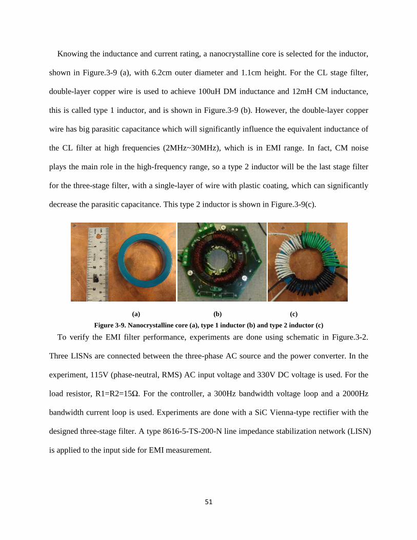
51
Knowing the inductance and current rating, a nanocrystalline core is selected for the inductor,
shown in Figure.3-9 (a), with 6.2cm outer diameter and 1.1cm height. For the CL stage filter,
double-layer copper wire is used to achieve 100uH DM inductance and 12mH CM inductance,
this is called type 1 inductor, and is shown in Figure.3-9 (b). However, the double-layer copper
wire has big parasitic capacitance which will significantly influence the equivalent inductance of
the CL filter at high frequencies (2MHz~30MHz), which is in EMI range. In fact, CM noise
plays the main role in the high-frequency range, so a type 2 inductor will be the last stage filter
for the three-stage filter, with a single-layer of wire with plastic coating, which can significantly
decrease the parasitic capacitance. This type 2 inductor is shown in Figure.3-9(c).
(a) (b) (c)
Figure 3-9. Nanocrystalline core (a), type 1 inductor (b) and type 2 inductor (c)
To verify the EMI filter performance, experiments are done using schematic in Figure.3-2.
Three LISNs are connected between the three-phase AC source and the power converter. In the
experiment, 115V (phase-neutral, RMS) AC input voltage and 330V DC voltage is used. For the
load resistor, R1=R2=15Ω. For the controller, a 300Hz bandwidth voltage loop and a 2000Hz
bandwidth current loop is used. Experiments are done with a SiC Vienna-type rectifier with the
designed three-stage filter. A type 8616-5-TS-200-N line impedance stabilization network (LISN)
is applied to the input side for EMI measurement.

52
3.3 Coupling issue for input EMI filter
All of the designs are based on the ideal model of inductor and filter. However, the parasitic
parameters embedded in the components will influence the filter performance, especially in the
high-frequency range. The most important issue is the equivalent series inductance (ESL) in the
final-stage capacitor, as shown in Figure.3-10. There are couplings between the ESL of C2 and
L1 and L2. Because the noise in the inductor is much bigger than the noise in C2, even though
the coupling inductance is very small, it will significantly influence the filtering performance of
the filter. Figure.3-11 shows the three-stage filter attenuation curve when there is 100pH
coupling between C2 and L2 and 10pH coupling between C2 and L1, in high frequency range
(10MHz~30MHz), the attenuation with the coupling has more than 20dB error than the ideal
filter. If the coupling inductance can be decreased to 20%, the attenuation can be improved more
than 10dB.
Figure 3-10. Coupling in the three-stage filter
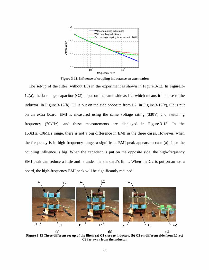
53
Figure 3-11. Influence of coupling inductance on attenuation
The set-up of the filter (without L3) in the experiment is shown in Figure.3-12. In Figure.3-
12(a), the last stage capacitor (C2) is put on the same side as L2, which means it is close to the
inductor. In Figure.3-12(b), C2 is put on the side opposite from L2, in Figure.3-12(c), C2 is put
on an extra board. EMI is measured using the same voltage rating (330V) and switching
frequency (70kHz), and these measurements are displayed in Figure.3-13. In the
150kHz~10MHz range, there is not a big difference in EMI in the three cases. However, when
the frequency is in high frequency range, a significant EMI peak appears in case (a) since the
coupling influence is big. When the capacitor is put on the opposite side, the high-frequency
EMI peak can reduce a little and is under the standard’s limit. When the C2 is put on an extra
board, the high-frequency EMI peak will be significantly reduced.
(a) (b) (c) Figure 3-12 Three different set-up of the filter: (a) C2 close to inductor, (b) C2 on different side from L2, (c)
C2 far away from the inductor
106
107
10-15
10-10
10-5
100
frequency / Hz
Atte
nuat
ion
Without coupling inductanceWith coupling inductanceDecreasing coupling inductance to 20%

54
Figure 3-13. Comparison of the EMI in the three different set-ups of the filter
3.4 Input EMI noise reduction by Random PWM
In the mid-frequency range (150kHz~10MHz), the linearity of the input filter stays nearly the
same as the designed value. The method for reducing the EMI noise will not be based on
parasitic parameters. Constant switching frequency space vector pulse width modulation
(SVPWM) is applied in the rectifier. As displayed in Figure.3-13, obvious oscillation in the EMI
noise can be found. The peak of the EMI noise is close to the standard. This is because that the
power of the switching voltage is focused near the harmonics of the switching frequency. When
designing the EMI filter, the corner frequency is selected to meet the requirement of the worst
case. In order to minimize the size of the filter, the switching frequency is selected in [1]. 70 kHz
and 140 kHz are selected since they can push the filter corner frequency to be high and satisfy
the EMI standard. For a 70kHz switching frequency, the second-order harmonic of the switching
frequency (140kHz) can avoid the EMI standard’s lower-limit (150kHz). However, the higher
harmonics of the switching frequency still produce the worst EMI noise, shown by Figure.3-13.
106
107
0
10
20
30
40
50
60
frequency / Hz
Noi
se /
dBuA
StandardCap and inductor in different side Cap far awayCap and inductor in the same side
55
Random PWM (RPWM) is an improved SVPWM method using a non-constant switching
frequency. By changing the switching frequency, the noise energy will be spread in a wider
frequency range and the peak noise in the harmonics of the switching frequency will be reduced.
This idea has been applied to inverters [45]-[47]. By applying this idea to high-frequency Vienna-
type rectifiers, the input current EMI noise peak can also be reduced. The switching frequency
should vary within a range much higher than the current controller frequency so the RPWM
method will not influence the low frequency component of the current. It will also not impair the
power quality of the current.
In order to verify the function of RPWM, theoretical Fourier analysis has been done for a
phase voltage waveform. The phase voltage in the Vienna-type rectifier is determined by the
switching function, shown in Table.3-1. In the table, d is the duty cycle of the gate signal in the
switching period Ts.. In each switching period, the terminal voltage of the rectifier can be 0 and
2dcV± , which is determined by the gate signal and current direction. A waveform of the terminal
phase voltage of one line-period in a Vienna-type rectifier can be constructed by this table, with
330V DC bus voltage, 110V (RMS) input voltage and unity power factor, with both constant
switching frequency and random switching frequency. The waveforms of the phase voltage are
displayed in Figure.3-14 (a), using one line-cycle data. Using Fourier analysis to calculate the
spectrum of the phase voltage from 150kHz to 1MHz, the results are shown in Figure.3-14 (b).
The spectrum of 70kHz SVPWM is concentrated in integers of 70kHz, with the 9.7V maximum
value near 210kHz. The spectrum of 40kHz SVPWM is concentrated in integers of 40kHz, with
the 8.2V maximum value near 160kHz. However, with the RPWM switching frequency ranging
from 55kHz to 70kHz, the noise spreads out in a wider frequency range and the maximum

56
voltage is less than 5V. With an input filter, the theoretical EMI noise with the RPWM can be
less than SVPWM in the mid-frequency range.
Table 3-1. Theoretical terminal phase voltage of Vienna-type rectifier in each switching cycle
ss Td
tTd
2
1
2
1 +<<− sT
dt
2
1−< or sTd
t2
1+>
I in Either >0 or <0 >0 <0
V in 0
2dcV
2dcV−
(a) (b)
Figure 3-14. Theoretical calculation results of phase voltage of Vienna rectifier with 70kHz SVPWM, 40kHz SVPWM and RPWM (55kHz~70kHz) : (a)Waveform and (b) Spectrum
A similar conclusion is found with Saber simulation results, shown in Figure.3-15 and
Figure.3-16. The simulation was performed with 330V DC bus voltage, 5kW load and 70kHz
switching frequency. Using only a 100uH input inductor and no extra filter, the spectrum of the
input current around the EMI lower limit is shown in Figure.3-15 (a). Although the 140kHz
spectrum peak avoids the EMI range, the current noise peak (in dBµA) in the EMI range still has
obvious peak in 210kHz and 280kHz, the EMI is up to 100dB. Figure.3-16 shows simulation
results when using RPWM ranging from 55kHz~70kHz. The current spectrum is distributed
0 0.5 1 1.5 2 2.5
x 10-3
-200
0
200
Va
/ V
70kHz SVPWM
0 0.5 1 1.5 2 2.5
x 10-3
-200
0
200
Va
/ V
40kHz SVPWM
0 0.5 1 1.5 2 2.5
x 10-3
-200
0
200
time / sec
Va
/ V
RPWM
2 4 6 8 10
x 105
0
1
2
3
4
5
6
7
8
9
10
frequency / Hz
Har
mon
ics
/ V
70kHz SVPWM
RPWM
40kHz SVPWM

57
continuously, and the noise in the EMI frequency range is much smoother than it is with constant
frequency SVPWM, it is about 10dB less around 280kHz.
(a) (b) Figure 3-15. Simulation results of current spectrum in A and dBµA of the Vienna rectifier with only boost
inductor and using 70 kHz SVPWM
(a) (b) Figure 3-16. Simulation results of current spectrum in A and dBµA of the Vienna rectifier with only boost
inductor and using 55 kHz~70 kHz RPWM
In order to verify the performance of RPWM in Vienna-type rectifier, experiments are
performed. In the beginning of the DSP program, N random numbers ranging between 0 and 1
are generated by MATLAB and saved as rand[N] . At the beginning of the interruption program,
the PWM cycle is updated using (3-6) with a changing index between 1 and N. PWM_cycle0 is
the PWM cycle of the initial switching frequency f0. With the defined coefficient λ, the switching
frequency will change between f0/(1+ λ ) and f0 so the random PWM range can be changed with
f0 and λ. If PWM_cycle0 is defined as 1.4286×10⁻⁵s (70kHz), and coefficient λ=0.2727, the

58
switching frequency will change between 55kHz and 70kHz. If λ=0 the switching frequency will
be fixed at 70kHz.
])[1(0__ indexrandcyclePWMcyclePWM ×+×= λ (3-6)
The experimental results are shown in Figure.3-17~Figure.3-19. Figure.3-17 displays the
experimental results of the Vienna-type rectifier with 70kHz SVPWM and RPWM ranging from
55kHz to 70kHz, using random data number N=200. The waveforms are similar for both the
PWM methods. The line-to-line voltage (Vab) of the rectifier input voltage is a five-level PWM
waveform with a 660V peak-peak value. The DC-link voltages (Vc1, Vc2) are controlled with
error less than 3V. The input phase currents (take phase A as example) in the three cases have
the same fundamental value (25A/div). Their low-order harmonics (1kHz~18kHz) are displayed
in Figure.3.18. The low-order harmonics are similar in the three cases, with the 2kHz value
(fifth-order harmonic) as the biggest, and the peak current harmonic is less than 0.5A. This is
because the control bandwidth is much less than the switching frequency and the methods used
with PWM have very little influence on the low-order harmonics. RPWM can perform with
similar power quality to constant frequency SVPWM. The spectrums of line-to-line voltage in
the three cases are displayed in Figure.3-18. With 70kHz and 40kHz SVPWM, the integers of the
switching frequency have obvious harmonic peaks among the frequency range, with peak value
more than 40V in the second-order harmonic. However, with RPWM, the voltage spectrum can
be smoothly distributed in the frequency range, with a peak value less than 20V.
Using an EMI tester, the current EMI noises in the three different cases are measured and
shown in Figure.3-19. The results are measured using a spectrum analyzer with 1kHz bandwidth
and using the peak-mode. At 70kHz SVPWM (a) and 40kHz SVPWM (b) the EMI noises have
obvious oscillation in the mid-frequency range. This is because the EMI peak is concentrated

59
around the harmonics of switching frequency. However, with RPWM, although the average EMI
noise is similar with the constant frequency SVPWM, the oscillation of EMI is much less in
RPWM, which keeps the EMI noise below the standard.
(a) (b)
(c)
Figure 3-17. Experimental results of Vienna-type Rectifier with 70 kHz SVPWM (a), 40 kHz SVPWM (b) and 55~70 kHz RPWM (c)
(a) (b)
2 4 6 8 10 12 14 16 180
0.1
0.2
0.3
0.4
frequency / kHz
Ia /
A
100 200 300 400 5000
10
20
30
40
50
frequency / kHz
Vab
/ V
2 4 6 8 10 12 14 16 180
0.1
0.2
0.3
0.4
frequency / kHz
Ia /
A
100 200 300 400 5000
10
20
30
40
50
frequency / kHz
Vab
/ V

60
(c)
Figure 3-18. Fourier analysis results of the current and voltage of Vienna-type Rectifier: with 70 kHz SVPWM (a), 40 kHz SVPWM (b) and 55~70 kHz RPWM (c)
106
107
-10
0
10
20
30
40
50
60
frequency / Hz
No
ise
/ dB
uA
70kHz SVPWM
106
107
-10
0
10
20
30
40
50
60
frequency / Hz
No
ise
/ dB
uA
40kHz SVPWM
106
107
-10
0
10
20
30
40
50
60
frequency / Hz
No
ise
/ dB
uA
55kHz~70kHz RPWM
EMI Standard
Total EMI
EMI Standard
Total EMI
EMI Standard
Total EMI
Figure 3-19. Experimental results: EMI measurement results of three cases with three-stage filter, 330V DC voltage and 3.6 kW output power
3.5 Conclusions
For modern power electronics converters with high switching frequencies, the EMI problem
should be examined, especially for applications that require high reliability, like aircraft and
aerospace applications. This chapter studies EMI reduction of active front-end rectifiers for the
high density motor drives, using the Vienna-type rectifiers as an example. The EMI noise
2 4 6 8 10 12 14 16 180
0.1
0.2
0.3
0.4
frequency / kHz
Ia /
A100 200 300 400 500
0
10
20
30
40
50
frequency / kHz
Vab
/ V

61
reduction methods are based on the three-stage LC filter structure. The following conclusions
can be made:
(1) The EMI reduction requirements can be calculated by spectrum analysis of the voltage and
the corner frequency of the filter can be calculated and the ideal L and C value can be decided.
However, parasitic capacitance in the double-layer inductor windings is detrimental to the
performance of the inductors at high frequencies. The third-stage inductor should serve as a CM
choke for high-frequency CM noise reduction, with single layer winding and with plastic coating.
(2) In the high-frequency range, experimental results prove that the coupling inductance in the
filter will significantly influence the EMI reduction result in the final-stage capacitor. The
coupling between the final-stage capacitor and the two inductors should be reduced.
(3) After theoretical analysis of different PWM methods based on the switching function of
Vienna-type rectifiers, we determine that random PWM can spread the energy concentrated
around the harmonics of switching frequency to a wider range than constant frequency SVPWM,
and random PWM can decrease the noise peak. Experimental results prove that when using
random PWM, the peak EMI noise in mid-frequency range can be reduced without a significant
reduction in the power quality.

62
Chapter 4. Common-mode EMI Noise Attenuation for
the Inverter
Different from the input side EMI requirement, few standardized EMI requirements are
defined for the motor drive output side in many cases. The main EMI concern for the inverter
side is the common-mode EMI current (leakage current) goes through the motor grounding
parasitic capacitor to the ground. The principle of CM noise reduction is mainly different from
that of DM noise because of different sources and paths. This chapter mainly deals with the CM
EMI noise attenuation techniques for the inverter. The basic principle is introduced in 4.1; then
the PWM methods’ influence on the CM noise source is introduced in 4.2; experiments are done
and discussed in 4.3 and conclusions are made in 4.4, including the design and control criteria
for the motor drive CM noise reduction.
4.1 Introduction
For high density motor drive design and control consideration, common-mode (CM) voltage
appears in the voltage source inverter. The CM voltage drops between the motor drive and the
ground and generating CM current (leakage current) going through the parasitic capacitors to the
ground. The CM current is not only harmful for the motor insulation but also brings worse EMI
problem for the motor drive system [75]. Two main groups of methods are studied for CM noise
current reduction: the improved PWM methods and the CM choke to attenuate the CM current.
Several improved PWM methods with better CM voltage are developed in recent years[76]-[78].
On the path of CM noise current, CM choke is also studied to attenuate the CM current[79][80].

63
CM chokes are CM inductors which can achieve high CM inductance in the motor drive’s CM
noise path and are used to impede the CM noise current for motor drives.
Figure.4-1 shows a typical AC-fed motor drive with CM choke and its grounding, the AC side
neutral point is connected to the power ground directly, the motor shell is also connected to the
power ground. Parasitic capacitance is existed between the motor windings and the motor shell,
and then there would be paths for the current going through the parasitic capacitors to the power
ground and back to the source side. Similarly, Figure.4-2 shows the case of DC-fed motor (VSI).
For safety issues the DC source is usually connected to the power ground, in order to reduce the
insulation standard the mid-point is used as the ground point for many cases like aircraft and ship.
The leakage current could go through the motor grounding capacitors and back to the DC source.
Both the two cases are based on the inverter CM voltage as noise source. In this chapter, the DC-
fed motor drive is used to study the methodology of CM noise attenuation for the inverter,
similar conclusions can also be valid for the AC-fed motor drive.
Figure 4-1. AC-fed motor drive with grounding
Figure 4-2. DC-fed motor drive with grounding

64
Figure.4-3(a) displays the equivalent circuit of a typical two-level inverter based motor drive
CM path with CM choke. The inverter output terminal voltages reference to O are Vao, Vbo and
Vco which are switching between Vdc/2 and -Vdc/2. Lcm is the CM choke connected between the
inverter and the motor. Rs and Ls are the motor stator resistance and inductance and ea, eb, ec are
the motor back-EMFs which are balanced. The equivalent single CM path is shown in Figure.4-
3(b) as a R-L-C series circuit, similar with reference[79]. The CM voltage source is
VCM=(Vao+Vbo+Vco)/3. Cs is the equivalent grounding capacitance between motor neutral point
and DC-link, usually with tens of nF value for 10kW level motor drive[79].
(a)
≈
(b)
Figure 4-3. Equivalent circuit for VSI based motor drive CM path: (a) three-phase equivalent circuit (b) CM
path
The main idea for the improved PWM methods is reducing the CM voltage peak from Vdc/2
to Vdc/6 including the active zero state PWM (AZSPWM1~3), the remote state PWM (RSPWM)
and the near state PWM (NSPWM). Among these PWM methods, the AZSPWM1 and NSPWM
are usually preferred[76]-[78]. The influence of PWM on the CM current is discussed in 4.2.
CM choke usually takes up to 25% of the system volume. Reference [79] claims that the
saturation of the flux in the CM choke caused by CM volt-second is the main factor determining
the CM choke size. However, reference [79] only studied the saturation case with SPWM whose
positive and negative volt-seconds are equal within one switching cycle. With most of the PWM
methods, low-frequency common-mode components are embedded in the modulation signals, the
volt-seconds are more complex. For high speed motor the influence of the low-frequency

65
components is more serious. The influence of PWM methods on the CM choke size are also
studied in 4.2.
Experiments are done to study the influence of PWM methods on CM noise and CM choke
saturation. Experiments are done with inverter driving R-L load, CM capacitor is build up to
emulate the CM loop, discussed in 4.3.
4.2 Different PWM Methods on the Noise Source
In 4.2, the PWM methods’ impact are studied for the noise source, the CM noise current and
CM choke volt-seconds.
4.2.1 CM noise source analysis
Four typical PWM methods are compared in this paper. The gate logics and the corresponding
CM voltage are displayed in Figure.4-4. Figure.4-4(a) shows the case of most common-used
SVPWM with CM voltage peak to be ±Vdc/2; Figure.4-4(b) and Figure4-4(c) show the case of
DPWM, one of the three phases is clamped to either positive or negative bus and the switching
loss could be reduced; AZSPWM1 is a variation for SVPWM but reduces the CM voltage peak
to be ±Vdc/6, shown in Figure.4-4 (d); similarly, NSPWM is a variation for DPWM and reduces
the CM voltage peak to be ±Vdc/6. NSPWM can both reduce the switching loss and CM voltage,
but it could not work with low modulation index, for CM voltage reduction purpose,
combination of AZSPWM1 and NSPWM is preferred[76]-[78].

66
ga
gb
gc
2/dcV6/dcV
6/dcV−2/dcV−
Vcm
ga
gb
gc
2/dcV6/dcV
6/dcV−2/dcV−
Vcm
ga
gb
gc
2/dcV6/dcV
6/dcV−2/dcV−
Vcm
(a) (b) (c)
ga
gb
gc
6/dcV
6/dcV−Vcm
(d)
ga
gb
gc
6/dcV
6/dcV−Vcm
(e)
Figure 4-4. Gate logic and CM voltage for: (a) SVPWM; (b) DPWM (clamped to positive bus); (c) DPWM (clamped to negative bus); (d) AZSPWM; (e) NSPWM
The main difference between SVPWM and DPWM is the arrangement of zero vectors and the
modulation signals for all the discussed PWM methods are the combinations of SPWM and
certain CM modulation signals [39]. The CM modulation signals for SVPWM and DPWM are
shown in (4-1) and (4-2). Beside the CM voltage in one switching period in Figure.4-4, these
CM modulation signals also contribute to the CM voltage. Figure.4-5 shows the modulation
signals of SPWM, SVPWM and DPWM. Figure.4-6 shows the CM modulation signal for
SVPWM (also AZSPWM) and DPWM (also NSPWM) under different modulation indexes.
With higher modulation index, the CM modulation signal of SVPWM increases but the CM
modulation signal of DPWM.
))1()1((2
1minmax uuucm −−+−= (4-1)
≤−−
>−=
minmaxmin
minmaxmax
),1(
),1(
uuu
uuuucm (4-2)
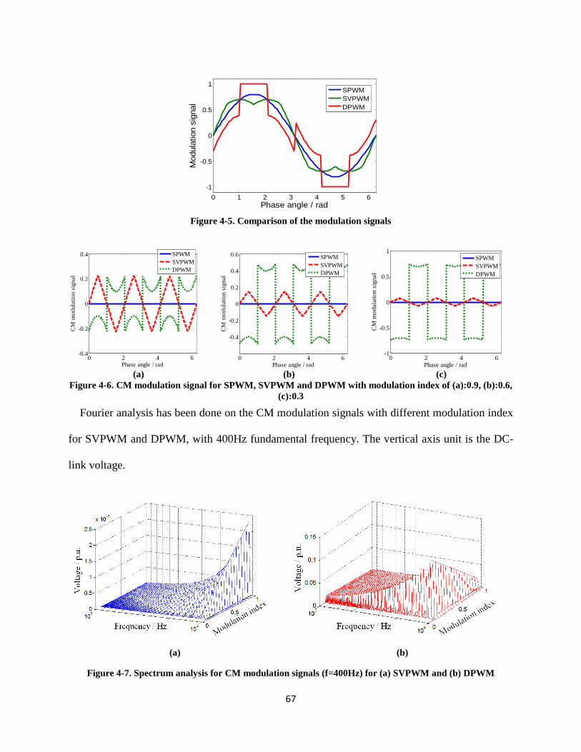
67
Figure 4-5. Comparison of the modulation signals
(a)
(b)
(c)
Figure 4-6. CM modulation signal for SPWM, SVPWM and DPWM with modulation index of (a):0.9, (b):0.6, (c):0.3
Fourier analysis has been done on the CM modulation signals with different modulation index
for SVPWM and DPWM, with 400Hz fundamental frequency. The vertical axis unit is the DC-
link voltage.
(a) (b)
Figure 4-7. Spectrum analysis for CM modulation signals (f=400Hz) for (a) SVPWM and (b) DPWM
0 1 2 3 4 5 6
-1
-0.5
0
0.5
1
Phase angle / rad
Mod
ulat
ion
sign
al
SPWMSVPWMDPWM
0 2 4 6-0.4
-0.2
0
0.2
0.4
Phase angle / rad
CM
mod
ula
tion
sign
al
SPWMSVPWMDPWM
0 2 4 6
-0.4
-0.2
0
0.2
0.4
0.6
Phase angle / rad
CM
mod
ulat
ion
sign
al
SPWMSVPWMDPWM
0 2 4 6-1
-0.5
0
0.5
1
Phase angle / radC
M m
od
ula
tion
sig
nal
SPWMSVPWMDPWM

68
With Figure.4-7, the harmonics of CM modulation signals with DPWM is obviously bigger
than with SVPWM in a wider range, especially with lower modulation index. Even with high
modulation index (0.9), the high frequency spectrum of DPWM is much bigger than SVPWM.
The comparison of CM modulation signal spectrum is shown in Figure.4-8.
Figure 4-8. Comparison of spectrum of CM modulation signal between SVPWM and DPWM with m=0.9
The CM loop (Figure.4-3(b)) equivalent circuit impedance is shown in (4-3). The resonant
frequency isscmCL
fππ
ω2
1
2== . With grounding capacitance of 10nF, if the CM choke
inductance is designed to be 2mH, the resonant frequency is 35kHz, with 8mH, the resonant
frequency will be 17.5kHz. In Figure.4.8, the CM modulation signal harmonics of DPWM near
these resonant frequencies has big contribution to CM current, which makes the CM current of
DPWM could be influenced much more than SVPWM. The transfer function bode plot is shown
in Figure.4-9. The peak point of the transfer gain waveform is the place where the CM current be
amplified most.
s
scms
scm
s
Cj
CLR
CjLj
RZ
ωω
ωω
21
3
1
3
−+=++= (4-3)
104
1050
0.005
0.01
0.015
0.02
0.025
0.03
0.035
Frequency / Hz
Vol
tage
/ p
.u.
DPWMSVPWM

69
Figure 4-9. CM loop current transfer gain with typical parameters
Although AZSPWM and NSPWM could effectively reduce the CM voltage peak, they make
the CM voltage turning points more. With spectrum analysis shown in Figure.4-10(a), the
voltage spectrums are compared between SVPWM and AZSPWM, and DPWM with NSPWM in
Figure.4-10(b).
(a)
(b)
Figure 4-10. CM voltage and its spectrum with 400Hz fundamental frequency and m=0.9
(a) SVPWM vs.AZSPWM and (b) DPWM vs. NSPWM
In Figure.4-10(a), although the CM voltage amplitude of AZSPWM is reduced to 1/3 of
SVPWM, its turning points are more, which makes the some orders harmonics of switching
frequency bigger in AZSPWM than SVPWM. Although the difference is small, with proper CM
resonant frequency the CM current could be amplified. The more obvious phenomenon can be

70
found in Figure.4-10(b), but for Figure.4-10(b), NSPWM also generates more 3rd order
harmonics of switching frequency than DPWM. With lower modulation index, the CM voltage
and its spectrum are shown in Figure.4-11 for comparison. Figure.4-11(a) is the comparison
between SVPWM and AZSPWM, some of the high order harmonics of switching frequency with
AZSPWM is bigger than SVPWM; Figure.4-11(b) is the comparison between DPWM and
NSPWM, discussed in reference [76]-[78], with low modulation index, NSPWM could not
achieve CM voltage amplitude reduction, and with low modulation index, CM modulation signal
influenced low frequency components is obviously bigger than with SVPWM/AZSPWM. With
AZSPWM and NSPWM, the CM modulation signal related harmonics (low frequency) do not
improve for SVPWM and DWM, because they are using the same CM modulation signals shown
in Figure. 4-6.
(a)
(b)
Figure 4-11. CM voltage and its spectrum with 400Hz fundamental frequency and m=0.3
(a) SVPWM vs. AZSPWM and (b) DPWM vs. NSPWM
4.2.2 CM noise current analysis
If the resonant frequency of the CM loop is close to the harmonics of switching frequency
where improved PWM methods (AZSPWM/NSPWM) CM voltage is bigger than

71
SVPWM/DPWM, the CM current of AZSPWM will be amplified and greatly reduce the benefit
of the improved PWM methods on CM noises.
For example, for the switching frequency is designed to be 12.5kHz, the choke inductance
should designed to make the resonant frequency avoid 37.5 kHz for NSPWM when m=0.9
because the 3rd order harmonics of NSPWM CM voltage is obviously bigger than DPWM and
the CM current will be amplified.
Assuming 10nF grounding capacitance and 2mH designed CM choke inductance, the resonant
frequency is kHzCL
fscm
352
1
2===
ππω
, with 12.5kHz switching frequency, the CM current
comparison is shown in Figure.4.12(a), because in Figure.4-10(b), NSPWM could achieve
obviously bigger 3rd order harmonics in CM voltage (37.5kHz) which is very close to the
resonant frequency, the CM current of NSPWM is greatly amplified and bigger than DPWM,
shown in Figure.4-12 (a), the benefit of CM voltage reduction in NSPWM could not achieve
better CM current; if change the switching frequency to 40kHz, the 3rd order harmonics (120kHz)
is far away from the resonant frequency, the CM current is greatly attenuated and the CM current
of NSPWM is obviously smaller than with DPWM, shown in Figure.4-12(b), the benefit of CM
voltage reduction for NSPWM could generate smaller CM current.

72
(a) (b)
Figure 4-12. CM current comparison between NSPWM and DPWM (m=0.9) with switching frequency:
(a) 12.5kHz, (b) 40kHz
Similar kinds of design consideration could also been developed in SVPWM/AZSPWM
comparison. Although AZSPWM could greatly reduce the CM voltage amplitude and the
component of switching frequency, when modulation index is low (m=0.3 for example), in the
voltage spectrum in Figure.4-11(b), the 5th order harmonic CM voltage of AZSPWM is bigger
than SVPWM. With the CM resonant frequency of 35 kHz (Lcm=2mH, Cs=10nF), if switching
frequency is 7kHz, the comparison of CM current of AZSPWM and SVPWM is shown in
Figure.4-13(a). Although AZSPWM reduced the CM voltage amplitude to 1/3, the 5th order
harmonics is obviously amplified and making the CM current amplitude more than SVPWM.
This is because the 5th order switching frequency is very close to the CM path resonant
frequency. When switching frequency increases to 20kHz, comparison is shown in Figure.4-
13(b), because the 5th order of switching frequency is far away from the CM loop resonant
frequency, the CM current of AZSPWM is not amplified, and the benefit of CM voltage
attenuation is also generating smaller amplitude of CM current.

73
(a)
(b)
Figure 4-13. CM current comparison between AZSPWM and SVPWM (m=0.3) with switching frequency:
(a) 7kHz, (b) 20kHz
The CM modulation signal could also obviously influence the CM current together with CM
loop impedance. DPWM could have more low frequency CM voltage than SVPWM in low
modulation index region because of the CM modulation signals. Assuming 300Hz fundamental
frequency for the motor and 20kHz switching frequency, with modulation index of 0.3, the
comparison of CM voltage with SVPWM and DPWM is shown in Figure.4-14. If the CM
resonant frequency is around the switching frequency, the CM current contributed by the CM
modulation signal will be low, but when the resonant frequency is lower (for example, around
10kHz) the impact will be big.
Figure 4-14. CM voltage spectrum comparison (f=300Hz,fs=20kHz,m=0.3)

74
Simulation results are shown in Figure.4-15. With CM choke inductance to be 8mH, when
Cs=10nF, the resonant frequency (18kHz) is close to switching frequency (20kHz), comparison
is shown in Figure.4-15(a), the CM current amplitude with DPWM is smaller than SVPWM, the
CM modulation signal does not contribute much to the CM current in DPWM because the
resonant frequency is too high. But when the CM resonant frequency is reduced to 10kHz
(Cs=30nF), the CM current of DPWM will be obviously bigger than SVPWM, because the CM
modulation signal based CM current is dominating the total CM current now, shown in Figure.4-
15(b).
(a)
(b)
Figure 4-15. CM current comparison between SVPWM and DPWM (m=0.3) with
(a) Cs=10nF, (b) Cs=30nF
The discussion in Chapter 4.2.2 analyzes the CM voltage differences with different PWM
methods, together with the CM loop model. The improved PWM methods could reduce the CM
voltage amplitude, but also brings some more high frequency components, when CM resonant
frequency is close to these components, the benefit of CM voltage reduction could not bring CM
current improvement. The application of PWM method for CM noise reduction should do
together with CM loop resonant frequency.

75
4.2.3 CM choke volt-seconds analysis
For the CM choke, its size is highly depends on the saturation flux generated by CM volt-
seconds[79]. In this chapter, CM choke is based on a toroid core with three-phase windings,
shown in Figure.4-16.
Figure 4-16. Three-phase CM choke structure
The flux in the core is the combination of phase-A winding (ia) and phase-B (ib) and phase-C
(ic) winding. The CM inductance is derived by (4-4), Ac is the cross-area and l is the core length.
With the maximum flux density in the core (Bmax), it can be expressed by (4-5). From (4-4) and
(4-5) the main volume of the inductor can be expressed by (4-6).
l
AN
li
AiN
i
NBA
iL cr
cm
ccmr
cm
c
cm
cmcm
20
20 33 µµµµψ ==== (4-4)
c
choke
c NA
dtV
NA
dB maxmax
max
∫∫ ==ψ
(4-5)
2max
max
2
02
max
max2
02
0 3)(
33
B
dtV
LNB
dtV
L
N
L
ANAlAV
choke
cm
rchoke
cm
r
cm
crcccore
∫∫==×=×= µµµµµµ (4-6)
From (4-6), with the designed CM inductance Lcm and the material character (Bmax and µr), the
volume is proportional to the square of CM volt-seconds. Then for high density motor drive
design and control, minimum volt-seconds should be achieved. Figure.4-17 shows the CM volt-
seconds for the CM voltage source for SPWM, SVPWM and DPWM in one switching cycle.
Only for SPWM, the source CM voltage can reset to its original value within one switching cycle.
For SVPWM and DPWM because of the CM modulation signal, the sum of the three-phase duty

76
cycles is different from 1.5 and the low frequency volt-second appears. DPWM has the worst
low frequency volt-second because of its CM modulation signal.
(a)
(b)
(c)
Figure 4-17. Volt-seconds demonstration for the CM voltage source in one switching cycle: (a) SPWM; (b) SVPWM; (c) DPWM
With the equivalent circuit in Figure.4-3(b), the CM voltage components dropped on the
choke is based on (4-7), Vsource is the component of source CM voltage with frequency of ω.
source
cms
cmchoke V
LR
LV
22
20222 )1(
9
1
ωωω
ω
−+=
(4-7)
The worst case for CM choke is that all the CM voltage is dropped on the choke, which means
AC and DC mid-points are directly connected. Then the volt-seconds are the source CM volt-
seconds, shown in Figure.4-17. In this worst case, the CM modulation signal will play a big role.
For example, with 400Hz fundamental frequency and 12.5kHz switching frequency, the CM
source volt-seconds for SVPWM and DPWM are shown in Figure.4-18. In one line-cycle
(2.5ms), the CM volt-seconds have 6 peak points which appear in each 1/6 cycle, mainly caused
by CM modulation signals. The oscillation of the CM volt-seconds are caused by the CM voltage
in each switching cycle as in Figure.4-17, mainly perform as the CM volt-seconds ripples.
With lower modulation index, CM modulation index in SVPWM is lower but in DPWM is
much bigger, causing the CM volt-seconds amplitude of DPWM is much bigger than SVPWM.

77
(a)
(b)
Figure 4-18. Source CM volt-seconds comparison (a): SVPWM; (b): DPWM
When using the improved PWM methods (AZSPWM and NSPWM), the CM voltage source
volt-seconds are shown in Figure.4-19 in comparison with SVPWM and DPWM. AZSPWM and
NSPWM could improve the volt-seconds in each switching cycle, but for the CM modulation
index determined volt-seconds they keep the same. In the volt-seconds waveform, the
improvement is the volt-seconds ripple reduction.
(a)
(b)
Figure 4-19. Source CM volt-seconds (m=0.9) comparison (a): SVPWM vs. AZSPWM; (b): DPWM vs. NSPWM
Most of the case, CM voltage will only partially drop on the choke, the choke size is
determined only by volt-seconds drop on itself, show in (4-8). In (4-8), Vcmk is the amplitude of
the CM voltage with kth order harmonics ωk. Writing (4-8) in s-domain, the volt-seconds on

78
choke is shown in (4-9), which shows that the maximum volt-seconds on the choke is determined
by the peak CM current value Icm. In (4-8), the voltage drop on the choke is determined by the
impedance of CM choke over the impedance of the whole CM loop. In the similar case of CM
current analysis (Cs=10nF), the ratio is shown in Figure.4-20(a). With the CM voltage drop on
the choke, the CM volt-seconds on the choke are shown in Figure.4-20(b) in frequency domain.
From Figure.4-20, the CM volt-seconds also have resonant peak and will amplify the
corresponding components near the resonant frequency.
)
)1(9
1)sin(max(
1 22
20222
max ∑∫∞
= −++=
k
cms
cmkkkcmk dt
LR
LtVVS
ωωω
ωθω (4-8)
)()(
)(
)1(9
1)(
1)(
22
20222
sILsZ
LsV
LsR
sLsV
ssVS cmcm
cm
cmcm
cms
cmcm ==
−+=
ωω
(4-9)
(a) (b)
Figure 4-20. Frequency domain bode plot of (a) voltage drop on CM choke (b) CM choke volt-seconds
When designing the CM choke with certain inductance for CM current reduction, its size will
be determined by the amplitude of volt-seconds drop on the choke. Then the choke size problem
could be re-written as to achieve smallest CM current peak value, which is usually determined by
resonant frequency.

79
4.3 Experimental verification
For CM noise current study, experimental circuit is designed in experiments, shown in
Figure.4-21. Three-phase inductor (Ls=0.8mH) are used to represent the motor leakage
inductance. Three-phase CM choke (Lcm=7.5mH) with Ferret toroid core are used for CM
inductor. Load resistance is R=10Ω and ground capacitance is Cs.
Figure 4-21. Experimental circuit for CM noise
First, CM voltage source with different modulation schemes are realized. The PWM methods
are realized in the DSP of TMS320F28335. Figure.4-22 shows the realization of AZSPWM and
NSPWM on the basis of SVPWM and DPWM.
In Figure.4-22, PWM duty cycles are calculated as SPWM, and the CM modulator is also
calculated. Then the duty cycles of SVPWM and DPWM could be generated. The duty cycles
are then compared in the Carrier selection module to determine the inversed carrier wave. The
carrier waves for three phases are generated and the pulses are achieved.
Duty cycle
calculation
CM modulator
calculation
Carrier
selection
SPWMSVPWM/
DPWM
AZSPWM
/NSPWM
Figure 4-22. PWM generation diagram for experiments
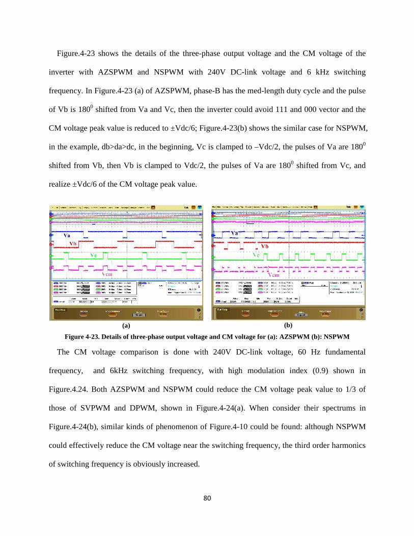
80
Figure.4-23 shows the details of the three-phase output voltage and the CM voltage of the
inverter with AZSPWM and NSPWM with 240V DC-link voltage and 6 kHz switching
frequency. In Figure.4-23 (a) of AZSPWM, phase-B has the med-length duty cycle and the pulse
of Vb is 1800 shifted from Va and Vc, then the inverter could avoid 111 and 000 vector and the
CM voltage peak value is reduced to ±Vdc/6; Figure.4-23(b) shows the similar case for NSPWM,
in the example, db>da>dc, in the beginning, Vc is clamped to –Vdc/2, the pulses of Va are 1800
shifted from Vb, then Vb is clamped to Vdc/2, the pulses of Va are 1800 shifted from Vc, and
realize ±Vdc/6 of the CM voltage peak value.
(a) (b)
Figure 4-23. Details of three-phase output voltage and CM voltage for (a): AZSPWM (b): NSPWM
The CM voltage comparison is done with 240V DC-link voltage, 60 Hz fundamental
frequency, and 6kHz switching frequency, with high modulation index (0.9) shown in
Figure.4.24. Both AZSPWM and NSPWM could reduce the CM voltage peak value to 1/3 of
those of SVPWM and DPWM, shown in Figure.4-24(a). When consider their spectrums in
Figure.4-24(b), similar kinds of phenomenon of Figure.4-10 could be found: although NSPWM
could effectively reduce the CM voltage near the switching frequency, the third order harmonics
of switching frequency is obviously increased.

81
(a) (b)
Figure 4-24. Experimental results: CM voltage comparison with m=0.9, 6kHz switching frequency and 60 Hz fundamental frequency (a): time domain (b): spectrum
When reducing the modulation index to be low (<0.5), NSPWM will not be able to work, the
comparison is only done for SVPWM and AZSPWM, shown in Figure.4-25. Similar with
analysis in Figure.4-11, when modulation index is low, the fifth order harmonics of switching
frequency of AZSPWM could be bigger than SVPWM, although the CM voltage amplitude is
greatly reduced.
Figure 4-25. Experimental results: comparison of CM voltage between SVPWM and AZSPWM (m=0.3)
With impedance analyzer, the transadmittance of the CM loop is measured for the
experimental testbed, shown in Figure.4-26. With 10nF grounding capacitance (Cs), the CM

82
transadmittance has its peak point (resonant point) near 18 kHz, and with Cs=30nF the resonant
frequency is reduced to about 10 kHz, which are close to the calculation results. Different from
theoretical analysis in Figure.4.9, in high frequency range some other peak points are found,
because of the parasitic parameters, but are much lower than the first peak. The CM current is
dominated by the first resonant peak value.
Figure 4-26. CM loop transadmittance for the experimental system
Experimental comparison between DPWM and NSPWM is shown in Figure.4-27. When
switching frequency is 6kHz, the 3rd order harmonics is close to the CM resonant frequency,
which means the bigger harmonics in NSPWM will be amplified and dominate the CM current.
Figure.4-27(a) shows that the CM current in NSPWM is bigger than DPWM, which is mainly
caused by the amplified 3rd order harmonics of the switching frequency. When switching
frequency is 20 kHz, as shown in Figure.4-27(b), the resonant frequency is close to the switching
frequency, and NSPWM could obviously reduce the CM current in this case.
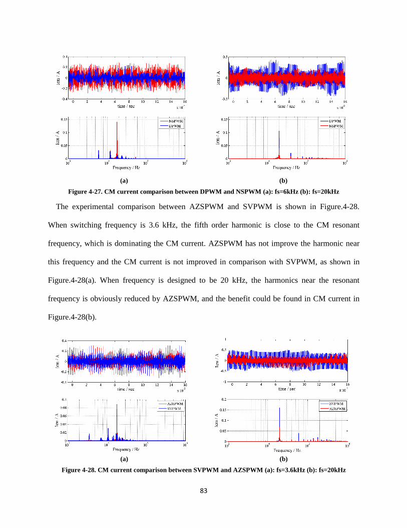
83
(a)
(b)
Figure 4-27. CM current comparison between DPWM and NSPWM (a): fs=6kHz (b): fs=20kHz
The experimental comparison between AZSPWM and SVPWM is shown in Figure.4-28.
When switching frequency is 3.6 kHz, the fifth order harmonic is close to the CM resonant
frequency, which is dominating the CM current. AZSPWM has not improve the harmonic near
this frequency and the CM current is not improved in comparison with SVPWM, as shown in
Figure.4-28(a). When frequency is designed to be 20 kHz, the harmonics near the resonant
frequency is obviously reduced by AZSPWM, and the benefit could be found in CM current in
Figure.4-28(b).
(a) (b)
Figure 4-28. CM current comparison between SVPWM and AZSPWM (a): fs=3.6kHz (b): fs=20kHz

84
When comparing with the conducted CM EMI, the benefit of AZSPWM and NSPWM is
limited, even with 20 kHz switching frequency, shown in Figure.4-29. The most obvious
improvements are found in the switching frequency, considering higher frequency range, little
significant improvement could be found.
(a)
(b)
Figure 4-29. Conducted EMI comparison (fs=20kHz), (a): SVPWM vs. AZSPWM; (b): DPWM vs. NSPWM
The CM modulation signal’s influence is also made into consideration. When m=0.3, the CM
modulation signal’s harmonics in DPWM is much bigger than SVPWM. When Cs=10nF, the
resonant frequency is 18kHz, much bigger than the fundamental frequency, in Figure.4-30(a), the
CM current with DPWM is bigger than with SVPWM in low frequency range, but the CM
current is still dominated by switching frequency component, the influence of CM modulation
signal is limited. When Cs is 30nF, as shown in Figure.4-30(b), the CM resonant frequency is
lower and the influence of CM modulation signal’s influence is bigger, but does not dominate the
CM current. When Cs is 50nF, the resonant frequency is reduced to 8 kHz, which is highly
impacted by the CM modulation signal based CM voltage, shown in Figure.4-14. Then the CM
current with DPWM is much bigger than SVPWM, mainly contributed by CM modulation
signals, shown in Figure.4-30(c).

85
(a) (b) (c)
Figure 4-30. Comparison of CM current between SVPWM and DPWM with low modulation index (m=0.3) (a): Cs=10nF, (b): Cs=30nF, (c): Cs=50nF
4.4 Conclusions Commom-mode (CM) noise is harmful for the motor drive and is one of the main concerns for
inverter. This chapter mainly studies the influence of PWM methods on the inverter output CM
noise and CM choke size for the high density motor drive. The CM noise source and path model
is studied in this chapter. For the noise source, different PWM methods are compared.
With the analysis and experiments for the inverter CM noise, the design and control issue for
motor drive with consideration of CM noise reduction is studied. Several conclusions could be
drawn:
(1) Based on conventional SVPWM and DPWM, AZSPWM and NSPWM are developed in
reference [76]-[78] to reduce the CM voltage of the inverter. Analysis and experiments
show that they do reduce the CM voltage output to be 1/3 of those of SVPWM and
DPWM. However, in spectrum analysis, those improved PWM methods bring some side
effects for harmonics of switching frequency, which is bigger than SVPWM and DPWM
in some orders of harmonics.
(2) The CM noise current is also highly depending on the CM loop impedance. Analysis and

86
experiments show that the inverter CM loop could be modeled as a L-C-R loop below
MHz frequency, and the resonant frequency is determined by the grounding capaictance
and CM inductance. CM current peak value is dominated by the current near the resonant
frequency.
(3) Improved PWM methods may generate higher CM current amplitude than conventional
PWM when the amplified CM voltage harmonics are close to the resonant frequency of
the CM loop. The CM conducted EMI for the improved PWM method is only obviously
improved near the switching frequency, for higher frequency range the improvement is
not obvious, or even worse.
(4) CM modulation signal in SVPWM and DPWM could also contribute to the CM voltage,
mainly are harmonics of fundamental frequency. DPWM has much bigger CM
modulation signal related CM harmonics than SVPWM in low modulation index. When
CM loop resonant frequency is closer to the fundamental frequency, DPWM will
generate higher CM modulation signal related CM noise current than SVPWM. But
usually this is not the dominating part in CM current amplitude.
(5) CM choke saturation is determined by the CM volt-seconds on the choke [79]. For the
worst case which all the CM voltage of the inverter drops on the choke, CM modulation
signal will be the dominating part for the CM volt-seconds. DPWM could generate much
bigger CM volt-seconds. For normal case, the CM volt-seconds peak value is similar with
CM current amplitude, reduction of CM current amplitude could also reduce the CM
choke size.
With these conclusions, the design and control criteria for motor drive with considerations of
CM noise reduction could be sumarized:

87
First, the design of PWM method and switching frequency should be together with the CM
loop impedance, but not simply selecting “better” PWM method. When using AZSPWM or
NSPWM to further reduce the CM noise, the switching frequency should be designed to make it
amplified harmonics avoiding the CM resonant frequency. Then their benefit of CM voltage
reduction could be used for CM noise current reduction.
Second, although DPWM/NSPWM could reduce the inverter switching loss, its CM
modulation signal is much bigger than SVPWM/AZSPWM in low modulation index region, and
will generate more CM noise, for the worst case for CM choke (AC netural connected to DC part
directly), the CM choke volt-seconds on the choke are serious for DPWM/NSPWM, too. DPWM
is not recommended for low modulation index application for CM noise consideration.

88
Chapter 5. Variable Switching Frequency PWM for
Loss and EMI Improvement
This chapter mainly deals with the design and application of variable switching frequency
PWM method to further improve the losses and EMI for the three-phase PWM converter.
Different from random PWM discussed in chapter 3, the variable switching frequency PWM
method is based on the theoretical analysis of current ripple in 5.2 and arranges the switching
frequency for current ripple requirement. In 5.3, the ripple current prediction is verified by
simulation results. In 5.4, variable switching frequency PWM control architecture is introduced
based on the ripple current prediction. Then based on two different kinds of current ripple
requirements, two variable switching frequency methods: VSFPWM1 and VSFPWM2 are
developed in 5.5 and 5.6 and verified by simulation results. Experimental testbed and results are
discussed in 5.7 to verify the methods. Then conclusions are made in 5.8.
5.1 Introduction
As discussed in chapter 3, constant switching frequency PWM (CSFPWM) methods are
widely used motor drive and other kinds of three-phase PWM converter applications. The main
reason is the simplicity of development of CSFPWM software. However, treating switching
frequency as a constant value in CSFPWM means lacking one of the important variables to
improve the converter performance. Recent years many efforts has been done to introduce
variable switching frequency PWM (VSFPWM) in motor drive and other kinds of three-phase
PWM converters. The most popular one is the random PWM (RPWM) method introduced in
chapter 3 for acoustic and EMI noises reduction. The principle of RPWM is randomly spread the
89
switching period for the converter to distribute the spectrum in a wider range than CSFPWM.
However, the results are based on statistical effect but not calculated. The converter losses and
current ripple under RPWM is not controllable.
Current ripple is an important requirement for design and control of three-phase PWM
converters. CSFPWM generates current ripple which is distributed not equally. Comparing with
CSFPWM, VSFPWM could achieve better current performance with the extra variable of
switching frequency. With understanding that current ripple is smaller in some of the range in
three-phase converter, reference [88] developed methods that double the switching frequency in
the area where the ripple current is bigger. This simple variation could reduce switching loss
with the similar ripple requirement. However, it is only a rough determination of the switching
frequency variation and could only roughly reduce current ripple in some area but without
theoretically arrangement. What is more, this method still depends on the harmonics of constant
switching frequency and could not improve EMI much. Another similar method is published in
reference [89], by adding pulses in the area where current ripple is bigger, similar kinds of
problem appears. Actually, a controllable VSFPWM instead of random PWM is preferred.
The main problem for recent VSFPWM methods for three-phase PWM converter is lacking
theoretically analysis of current ripple and could not design the switching frequency variation
laws to arrange the current ripple. Reference [18] discussed the harmonic flux and Harmonic
Distortion Function (HDF) to evaluate the ripple current, but mainly studied the overall effect
but not ripple current distribution in time-domain. Reference [42] and [43] proposed current
ripple improved PWM methods by arranging the pulses position in each switching period. These
papers have studied the details of current ripple in each switching period, but keeping the
constant switching frequency and have not studied the current ripple distribution. Reference [90]

90
and [91] extended these concepts to five-phase voltage-source converter and studied their
influence on the Total Harmonic Distortion (THD), but still not fully studied the current ripple
distribution and variable switching frequency.
Based on the detailed analysis of ripple current distribution, reference [44] proposed variable
switching frequency method for single-phase inverter. The ripple current in each switching cycle
could be predicted with the duty cycle d, switching period Ts, output inductance L and DC
voltage Vdc. Then the switching frequency could be arranged to control the current ripple to
satisfy certain requirements including peak current ripple and RMS current ripple requirement.
With the proposed VSFPWM methods, switching losses of single phase converter could be
reduced together with satisfying the ripple requirement.
The case of ripple current in three-phase converter is more complex than single phase since
the ripple current in each phase is influenced by the switching actions for all the three phases.
This chapter extends the similar principle of reference [44] to three-phase converter to fully
study the ripple current distribution for this kind of converters and build up the basis for the
ripple current prediction based VSFPWM method.
In 5.2, the switching ripple principle of three-phase PWM converter is studied and compared
in 5.3. Then the structure of ripple current prediction based VSFPWM architecture is proposed in
5.4 and two VSFPWM methods: VSFPWM1 and VSFPWM2 are introduced in 5.5 and 5.6, with
experimental verification in 5.7. Conclusions are made in 5.8.
5.2 Analytical Current Ripple Analysis for Three-phase PWM converter
In the modulator of the three-phase converter, da, db and dc are the duty cycles of the three
phases, varying from 0 to 1. Defining the “quasi-duty cycle” dx’ which varies from -1 to 1 by
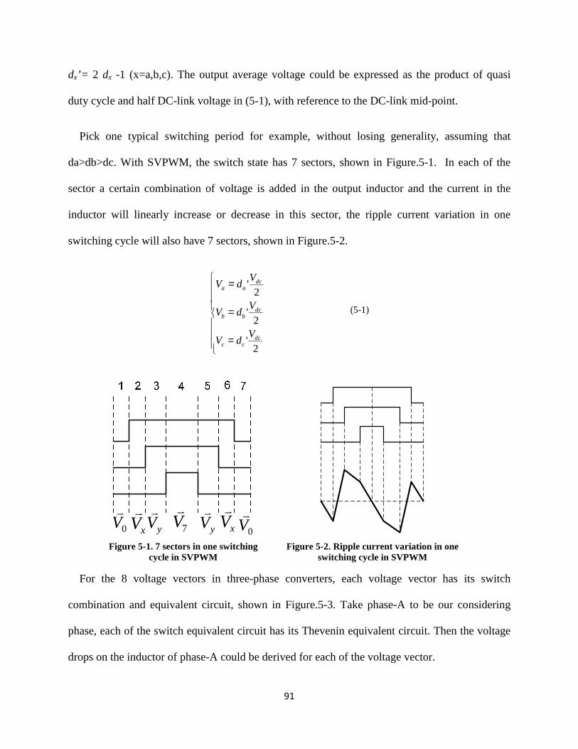
91
dx’= 2 dx -1 (x=a,b,c). The output average voltage could be expressed as the product of quasi
duty cycle and half DC-link voltage in (5-1), with reference to the DC-link mid-point.
Pick one typical switching period for example, without losing generality, assuming that
da>db>dc. With SVPWM, the switch state has 7 sectors, shown in Figure.5-1. In each of the
sector a certain combination of voltage is added in the output inductor and the current in the
inductor will linearly increase or decrease in this sector, the ripple current variation in one
switching cycle will also have 7 sectors, shown in Figure.5-2.
=
=
=
2'
2'
2'
dccc
dcbb
dcaa
VdV
VdV
VdV
(5-1)
0Vv
xVv
yVv
7Vv
yVv
xVv
0Vv
Figure 5-1. 7 sectors in one switching
cycle in SVPWM
Figure 5-2. Ripple current variation in one
switching cycle in SVPWM
For the 8 voltage vectors in three-phase converters, each voltage vector has its switch
combination and equivalent circuit, shown in Figure.5-3. Take phase-A to be our considering
phase, each of the switch equivalent circuit has its Thevenin equivalent circuit. Then the voltage
drops on the inductor of phase-A could be derived for each of the voltage vector.

92
(a) Vector 000
(b) Vector 100
(c) Vector 110
(d) Vector 111
(e) Vector 001
(f) Vector 010
(g) Vector 011
(h) Vector 101
Figure 5-3. Switch combination of 8 different voltage vectors and their Thevenin equivalent circuits
Take the voltage vectors in Figure.5-1 for example. In the first sector, vector )000(0Vv
is added,
the equivalent circuit of this switching state is shown in Figure.5-3(a). Based on the Thevenin
equivalent circuit of phase-B and phase-C paralleled branches, the equivalent circuit of this
switching state is also shown in Figure. 5-3(a). Then the current slope in phase-A inductor could
be derived and shown in (5-2), considering the average value of the phase voltage in (5-1), the
expression could be written in (5-3).
)2
(32
acba V
VV
Ldt
dI −+= (5-2)
)'2
''(
3 acbdca d
dd
L
V
dt
dI −+= (5-3)

93
In the second sector, vector xVv
is added, (in this case, xVv
=(100)), the equivalent circuit is
shown in Figure.5-3(b). Similar kind of Thevenin circuit is derived in Figure.5-3(b), too. The
current slope is derived as (5-4). In the third sector, vector yVv
is added, (in this case, yVv
=(110) ), the equivalent circuit is shown in Figure.5-3 (c). Similar kind of Thevenin circuit is
derived in Figure.5.3 (c), too. The current slope is derived as (5-5). In the fourth sector, vector
)111(7Vv
is added, the equivalent circuit of this switching state is shown in Figure.5-3 (d), together
with the Thevenin equivalent circuit. The slope of Ia is derived in (5-6).
)2
'
4
''1(
3
2 acbdca ddd
L
V
dt
dI −++= (5-4)
)2
'4
''21
(32 acbdca ddd
L
V
dt
dI −++= (5-5)
)'2
''(
3 acbdca d
dd
L
V
dt
dI −+= (5-6)
Then in the sector 5, 6 and 7, the voltage vectors and the current slope are the same with sector
3, 2 and 1, the current ripple waveform in this switching cycle is shown in Figure.5-2
In each switching-period of the three-phase converter, 4 of 8 voltage vectors are applied.
Based on the Thevenin equivalent circuit in Fig.3, the slope of the current ripple could be derived
and summarized in Table.5-1.
Table 5-1. Ripple current slope with different voltage vectors
Vector 000 )'2
''(
3 acbdca d
dd
L
V
dt
dI −+= Vector 001 )'12
''(
3 acbdca d
dd
L
V
dt
dI −−+=
Vector 100 )2
'
4
''1(
3
2 acbdca ddd
L
V
dt
dI −++= Vector 010 )'12
''(
3 acbdca d
dd
L
V
dt
dI −−+=
Vector 110 )2
'
4
''
2
1(
3
2 acbdca ddd
L
V
dt
dI −++= Vector 011 )2
'1
4
''(
3
2 acbdca ddd
L
V
dt
dI −−+=
Vector 111 )'2
''(
3 acbdca d
dd
L
V
dt
dI −+= Vector 101 )2
'
4
''
2
1(
3
2 acbdca ddd
L
V
dt
dI −++=

94
Similarly, the current ripple of phase B and phase C could also be analyzed like that.
If DPWM is used instead of SVPWM, the current ripple could be different, the ripple in one
switching cycle could have 5 linear sectors. The case with DPWM will also be studied in this
chapter. The analytical expressions of SVPWM and DPWM are studied based on Table.5-1.
40t
21t
22t
20t
22t
21t
40t
Figure 5-4. Current ripple in one switching cycle: SVPWM
For SVPWM, as shown in Fig.5.4, the current ripple in one switching cycle has 7 linear parts
in the whole switching cycle. The effective times for the 7 sectors are shown in Figure.5-4. The
current ripple is anti-symmetric between first and second half. Assuming the ripple current slope
for Vx and Vy are k1 and k2, calculated in Table.1. The ripple current turning point values are
shown in (5-7), the value of x and y could be either positive or negative. Then based on Figure.5-
4, the peak current ripple in one switching cycle is max(|x|,|y|). The ripple current RMS value
could also be derived from Figure.5-4, as shown in (5-8).
⋅+⋅=
⋅=
24
4
12
01
01
tk
tky
tkx
(5-7)

95
333
222
221
20 yxyx
T
tyxyx
T
tx
T
tI
sssrms
+−++++=∆ (5-8)
With DPWM, the minimum duty cycle is clamped to 0 or maximum duty cycle is clamped to
1, the corresponding current ripple in one switching cycle is shown in Figure.5-5(a) and
Figure.5-5(b). Different from SVPWM, the ripple current of DPWM only has five linear parts in
one switching period.
20t
21t
21t
20t
2t
(a)
21t
22t
22t
21t
0t
(b)
Figure 5-5. Current ripple in one switching cycle: DPWM (a) Clamped to negative bus, (b) Clamped to positive bus
For the DPWM in Figure.5-5, assuming ripple current’s slope under zero vector is k1, the
ripple current’s slope under the voltage vector near the zero vector is k2, then the ripple current
turning value could be written in (5-9). The current ripple peak in one switching cycle in DPWM
is also max(|x|,|y|), the ripple current RMS value could also be derived from Figure.5-5 as (5-10).
−⋅+⋅
−⋅+⋅=
⋅=
))(55.(22
))(55.(22
2
22
01
12
01
01
bFiguret
kt
k
aFiguret
kt
ky
tkx
(5-9)

96
−++++
−++++=∆
)55.(333
)55.(333
221
22
20
222
21
20
bFigureyxyx
T
ty
T
tx
T
t
aFigureyxyx
T
ty
T
tx
T
t
I
sss
sss
rms (5-10)
5.3 Ripple current comparison
Based on the analytical expressions developed in part II, ripple current could be predicted with
the modulation method, DC-link voltage Vdc, output inductance L and switching frequency fs.
The ripple current unit value is )3/( sdc LfV .
Figure.5-6 displays the analytical predicted waveform of current ripple in phase-A with
SVPWM, with modulation index of 0.9 and 0.5, including the waveform in the whole line-period
and the enlarged details in one switching cycle. Current ripple distribution in one line period is
varying and the ripple current in one switching period follows the 7 sector principle.
0 1 2 3 4 5 6
-0.2
-0.1
0
0.1
0.2
0.3
Phase angle / rad
Rip
ple
cu
rre
nt
/ p
.u.
3.125 3.13 3.135 3.14 3.145 3.15 3.155-0.2
-0.15
-0.1
-0.05
0
0.05
0.1
0.15
0.2
Phase angle / rad
Rip
ple
cu
rre
nt
/ p
.u.
(a) m=0.9
0 1 2 3 4 5 6-0.2
-0.15
-0.1
-0.05
0
0.05
0.1
0.15
0.2
Phase angle / rad
Rip
ple
cu
rre
nt
/ p
.u.
3.125 3.13 3.135 3.14 3.145 3.15 3.155-0.2
-0.15
-0.1
-0.05
0
0.05
0.1
0.15
Phase angle / rad
Rip
ple
cu
rre
nt
/ p
.u.
(b) m=0.5 Figure 5-6. Ripple current in one line-cycle: SVPWM
Similarly, ripple current could be re-constructed for DPWM, with the same cases. The
theoretical predicted current ripple waveforms are shown in Figure.5-7, with one line-period
waveform and enlarged detail in one switching cycle. Comparing with Figure.5-6, the current
ripple value is obviously larger with DPWM than SVPWM.

97
3.13 3.14 3.15-0.2
-0.15
-0.1
-0.05
0
0.05
0.1
0.15
0.2
Phase angle / rad
Rip
ple
cu
rren
t /
p.u
.
0 1 2 3 4 5 6
-0.2
-0.1
0
0.1
0.2
0.3
Phase angle / rad
Rip
ple
cu
rre
nt
/ p
.u.
(a) m=0.9
0 1 2 3 4 5 6-0.3
-0.2
-0.1
0
0.1
0.2
0.3
Phase angle / rad
Rip
ple
cu
rren
t /
p.u
.
3.13 3.14 3.15-0.2
-0.15
-0.1
-0.05
0
0.05
0.1
0.15
Phase angle / rad
Rip
ple
cu
rren
t /
p.u
.
(b) m=0.5 Figure 5-7. Ripple current in one line-cycle: DPWM
Then the peak value and RMS value of the current ripple could be calculated in the predicted
waveform. Figure.5-8 and Figure.5-9 displays the peak current ripple and RMS current ripple
(calculated in each switching cycle) for SVPWM and DPWM and with different modulation
index. DPWM achieves obviously higher ripple current peak and RMS value than SVPWM.
Figure 5-8. Comparison of ripple current peak-to-
peak value
Figure 5-9. Comparison of ripple current RMS value
Then by sweeping the modulation index from 0.1 to 1.1, the ripple current peak-to-peak value
could be predicted in Figure. 5-10. In the phase angle near 0.5π and 1.5 π, the ripple current peak
of DPWM is much bigger than SVPWM. Putting the two figures together, the results could be
seen in Figure.5-11, the ripple peak value of DPWM covers all that of SVPWM in the whole
range. Figure.5-12 shows the comparison of ripple current RMS value (calculated by (5-8) and
0 1 2 3 4 5 60.1
0.15
0.2
0.25
0.3
0.35
0.4
0.45
0.5
0.55
0.6
Phase angle / rad
Rip
ple
cu
rre
nt
pe
ak /
p.u
.
SVPWM, m=0.9SVPWM, m=0.5DPWM, m=0.9DPWM, m=0.5
0 1 2 3 4 5 60.02
0.04
0.06
0.08
0.1
0.12
0.14
0.16
Phase angle / rad
Rip
ple
cu
rren
t R
MS
val
ue
/ p
.u.
SVPWM m=0.9SVPWM m=0.5DPWM m=0.9DPWM m=0.5

98
(5-10)) with SVPWM and DPWM with different modulation index. DPWM could generate
obviously bigger ripple current RMS value than SVPWM and have bigger THD.
(a) SVPWM
(b) DPWM
Figure 5-10. Ripple current peak value variation with phase-angle and modulation index
Figure 5-11. Comparison of ripple current peak-to-
peak value
Figure 5-12. Comparison of ripple current RMS
value
Comparison between analytical results and simulation results are studied to verify the
prediction. The simulation model is simulated in MATLAB/SIMULINK as a grid-connected
inverter with 400V DC-link voltage and 500µH out-put inductor. The system circuit is shown in
Figure.5-13. This topology could represent general three-phase converter with AC loads like
motor, grid and passive loads. Ripple current in the simulation result is defined as the error
0.2 0.4 0.6 0.8 10
0.02
0.04
0.06
0.08
0.1
Modulation index
Rip
ple
cu
rre
nt
RM
S v
alu
e /
p.u
.
SVPWMDPWM

99
between phase-current and average model result. The predicted current ripple fits the simulation
result well for both SVPWM and DPWM.
Figure 5-13. Equivalent circuit for simulation
Figure.5-14 shows the three-phase current of the simulation results of the converter. The three
phases are well balanced, without losing of generality, phase-A is selected for analysis. Figure.5-
15 shows the phase current and its average value in one line-period (60Hz). The ripple current is
the error between phase current and its average value. Figure.5-16 shows the ripple current in
simulation and theoretical prediction in one line-period (60Hz). The enlarged details of the ripple
currents are also shown in Figure.5-17. The overall waveform of the simulation result is very
close to the theoretical predicted result, so does the enlarged details. Figure.5-17 shows that the
theoretical predicted current ripple peak value well fits the simulation results. FFT analysis has
been done for the phase current, shown in Figure.5-18, the ripple current RMS value is 0.798A
and THD is 11.2%, well fitting the theoretical predicted value (0.803A and 11.3%).
Figure 5-14. Simulation result: three-phase current with SVPWM (20kHz)
Figure 5-15. Simulation result: Phase current and its average value with SVPWM (20kHz)
0.48 0.485 0.49 0.495 0.5-15
-10
-5
0
5
10
15
time / sec
Ph
ase
curr
en
t /
A
Phase-APhase-BPhase-C
0.484 0.486 0.488 0.49 0.492 0.494 0.496 0.498 0.5-15
-10
-5
0
5
10
15
time / sec
Ph
ase
cu
rren
t /
A
Phase current Average value

100
0.484 0.486 0.488 0.49 0.492 0.494 0.496 0.498 0.5-4
-2
0
2
4Simulation result
time / sec
Rip
ple
cu
rre
nt
/ A
0 0.002 0.004 0.006 0.008 0.01 0.012 0.014 0.016-4
-2
0
2
4Theorectical prediction
time / sec
Rip
ple
cu
rren
t /
A
0.489 0.489 0.4891 0.4891 0.4892 0.4892
-1
0
1
time / sec
Rip
ple
cur
ren
t /
A
5.65 5.7 5.75 5.8 5.85 5.9
x 10-3
-1
0
1
time / sec
Rip
ple
cu
rre
nt /
A
0.49210.49220.49220.49230.49240.49240.4925
-2
0
2
time / sec
Rip
ple
curr
ent
/ A
8.85 8.9 8.95 9 9.05 9.1 9.15
x 10-3
-2
0
2
time / sec
Rip
ple
curr
ent
/ A
Figure 5-16. Comparison between simulation results and theoretical prediction with SVPWM: whole period and details
Figure 5-17. Comparison between theoretical predicted peak ripple and simulation results: SVPWM
Figure 5-18. Current spectrum of simulation result:
SVPWM
Figure.5-19 shows the simulation results of the three-phase current with DPWM for the same
case. Picking phase-A for example, the phase current and its average value is shown in Figure.5-
20. The ripple current comparison is shown in Figure.5-21 with one line-period waveform and
enlarged details, simulation results well fit the theoretical predicted current ripple value (the
small error is caused by simulation step precision). The predicted ripple current peak value also
fits the simulation results well in Figure.5-22. The spectrum analysis for phase current is shown
0 1 2 3 4 5 6-3
-2
-1
0
1
2
3
Phase angle / rad
Rip
ple
cu
rren
t /
A
Predicted peak valueSimulation result

101
in Figure.5-23, with 1.320A ripple current RMS value and the THD of 18.51%, which is nearly
the same with the predicted results of 1.320A and 18.51% .
Figure 5-19. Simulation result: three-phase current
with DPWM (20kHz)
Figure 5-20. Simulation result: Phase current and its
average value with DPWM (20kHz)
0.484 0.486 0.488 0.49 0.492 0.494 0.496 0.498 0.5-4
-2
0
2
4
time / sec
Rip
ple
cu
rren
t / A
Simulation result
0 0.002 0.004 0.006 0.008 0.01 0.012 0.014 0.016-4
-2
0
2
4
time / sec
Rip
ple
cu
rren
t /
A
Theoretical prediction
0.488 0.4881 0.4881 0.4882 0.4882 0.4883-4
-2
0
2
4
4.7 4.8 4.9 5
x 10-3
-4
-2
0
2
4
0.492 0.4921 0.4921 0.4922 0.4922 0.4923-4
-2
0
2
4
8.7 8.75 8.8 8.85 8.9 8.95 9
x 10-3
-4
-2
0
2
4
Figure 5-21. Comparison between simulation results and theoretical prediction with DPWM: whole period and details
Figure 5-22. Comparison between theoretical
predicted peak ripple and simulation results: DPWM Figure 5-23. Current spectrum of simulation result:
DPWM
0.48 0.485 0.49 0.495 0.5-15
-10
-5
0
5
10
15
20
time / sec
Ph
ase
cur
ren
t /
A
Phase-APhase-BPhase-C
0.485 0.49 0.495 0.5-15
-10
-5
0
5
10
15
time / sec
Pha
se c
urr
ent
/ A
Phase current Average value
0 1 2 3 4 5 6-4
-3
-2
-1
0
1
2
3
4
5
Phase angle / rad
Rip
ple
cur
rent
/ A
Simulation resultPredicted ripple peak
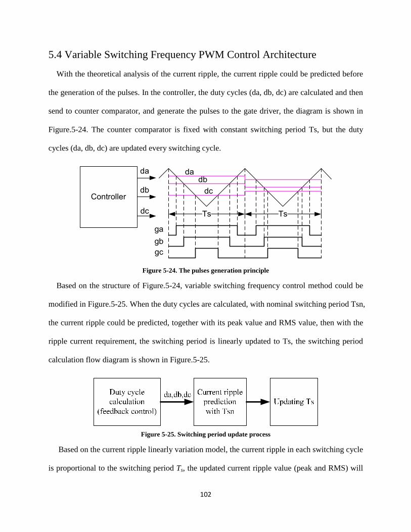
102
5.4 Variable Switching Frequency PWM Control Architecture
With the theoretical analysis of the current ripple, the current ripple could be predicted before
the generation of the pulses. In the controller, the duty cycles (da, db, dc) are calculated and then
send to counter comparator, and generate the pulses to the gate driver, the diagram is shown in
Figure.5-24. The counter comparator is fixed with constant switching period Ts, but the duty
cycles (da, db, dc) are updated every switching cycle.
Controller
Ts Ts
dadb
dc
ga
gb
gc
da
db
dc
Figure 5-24. The pulses generation principle
Based on the structure of Figure.5-24, variable switching frequency control method could be
modified in Figure.5-25. When the duty cycles are calculated, with nominal switching period Tsn,
the current ripple could be predicted, together with its peak value and RMS value, then with the
ripple current requirement, the switching period is linearly updated to Ts, the switching period
calculation flow diagram is shown in Figure.5-25.
Figure 5-25. Switching period update process
Based on the current ripple linearly variation model, the current ripple in each switching cycle
is proportional to the switching period Ts, the updated current ripple value (peak and RMS) will

103
follow (5-11). If the updated current is fixed to the required current Iripple_require, the updated
switching period is derived in (5-12).
sN
spredictedrippleupdateripple T
TII ×= __
(5-11)
requireripple
perdictedripplesNs I
ITT
_
_×= (5-12)
For example, in the calculation period k, duty cycles are calculated, and with nominal
switching period TsN (assuming nominal switching frequency is 20kHz, TsN =50µs) the current
ripple peak value is predicted to be 2A, if the requirement is defined to be peak ripple current
should be no bigger than 1A, in this switching period, Ts should be adjusted to 25µs and
generated in the next period.
Based on the switching cycle update method shown in Figure.5-25, the VSFPWM generation
diagram is shown in Figure.5-26. When the duty cycles of three phases are calculated in the
controller, they are sent to the current ripple prediction block with nominal switching frequency
and the predicted current ripple is sent to the switching period calculation block. With the current
ripple requirement, the updated switching cycle Ts is calculated and the triangle wave is
generated in the counter comparator, to compare with the duty cycle and generate the gate driver
pulses for the three phases.

104
Figure 5-26. Structure of variable switching frequency PWM generation
With different current ripple requirements, different VSFPWM methods could be applied to
the three-phase PWM converters. Usually, two kinds of current ripple requirements are
concerned: one is the current ripple peak value requirement, which influences the maximum
deviation of the ripple; the other is the current ripple RMS value requirement, which influence
the THD of the output current. Two kinds of VSFPWM methods are introduced next based on
these two different kinds of requirements and their benefits are discussed. Aiming at different
purpose, different kinds of variable switching frequency PWM methods could be achieved. In
this paper, two methods are introduced, one is to control the maximum ripple peak (VSFPWM1),
and the other is to control the ripple current RMS value (VSFPWM2).
In order to study the VSFPWM methods, a typical case of three-phase PWM converter is
simulated as the object, with the same parameters in 5.3.
5.5 Variable Switching Frequency PWM to Control Peak Current Ripple
(VSFPWM1)
For the application cares about the maximum deviation of the output current, the current ripple
current requirement is usually defined as the maximum current ripple peak. For example, the

105
current ripple peak could influence the motor’s maximum torque ripple peak and the noises
amplitude. For this kind of application, the current ripple is defined in a certain range. In the
discussion, ±1.4A is defined as the current ripple range as the example.
Problem of constant switching frequency PWM (CSFPWM) is that in different phase-angle,
the ripple current has different value. Even considering the maximum current ripple of all the
three phases, it is less than the range for most of the areas if using CSFPWM.
For the example case, with the DC-link voltage, the output inductance and modulation scheme,
the current ripple could be predicted for CSFPWM, and the switching frequency should be
designed to be 33.7 kHz to satisfy the current ripple requirement. The simulation results of the
three phases current are shown in Figure.5-27. The current ripples of the three phases are shown
in Figure.5-28. The ripple current could satisfy the requirement well. But in most of the time in
the line-period, the ripple is smaller than the required range. This means in these areas the
switching frequency is higher than just satisfying the range and there is a space to reduce the
switching frequency.
Figure 5-27. Result: three-phase current of constant switching frequency (33.7kHz) to fit the ripple requirement
0.385 0.39 0.395 0.4-15
-10
-5
0
5
10
15
time / sec
Cur
rent
/ A
Phase-APhase-BPhase-C

106
Figure 5-28. Simulation result: ripple current of constant switching frequency (33.7kHz) to fit the ripple requirement
The principle of the VSFPWM1 is using the switching period Ts to control the current ripple
peak value of the three phases within the certain range, following the control diagram in
Figure.5-26. The updating switching period follows Figure.5-29. The predicted current ripples of
the three phases are compared and the maximum current ripple Iripple_max is sent to the switching
period calculation block. With this kind of diagram, the switching period Ts is to keep the
maximum current ripple peak of the three phases to be the current ripple limited value.
Duty cycle
calculation
(feedback control)
Current ripple
(peak)
prediction
with Tsn
Max
da,db,dc
Aripplei _
Bripplei _
Cripplei _
requireripple
ripplesNs I
ITT
_
max_×=max_rippleI
Figure 5-29. Switching frequency update diagram for VSFPWM1
0.384 0.386 0.388 0.39 0.392 0.394 0.396 0.398 0.4-2
0
2
time / sec
Rip
ple
A /
A0.384 0.386 0.388 0.39 0.392 0.394 0.396 0.398 0.4
-2
0
2
time / secR
ipp
le B
/ A
0.384 0.386 0.388 0.39 0.392 0.394 0.396 0.398 0.4-2
0
2
time / sec
Rip
ple
C /
A
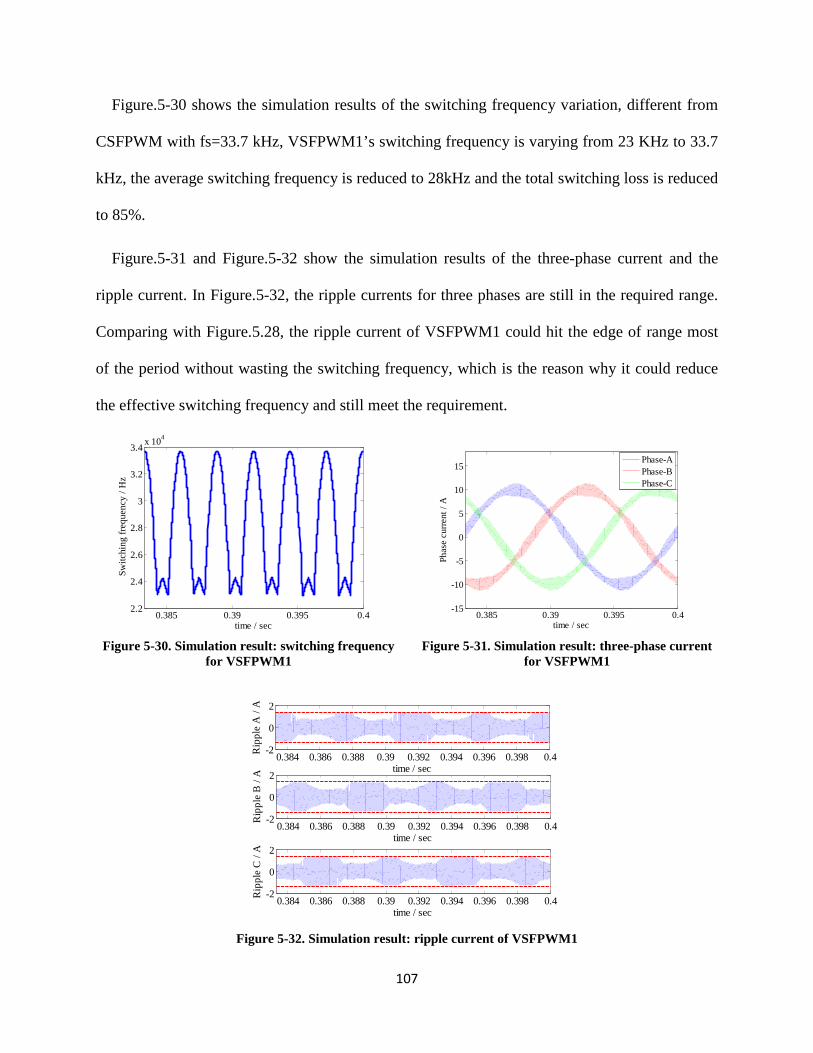
107
Figure.5-30 shows the simulation results of the switching frequency variation, different from
CSFPWM with fs=33.7 kHz, VSFPWM1’s switching frequency is varying from 23 KHz to 33.7
kHz, the average switching frequency is reduced to 28kHz and the total switching loss is reduced
to 85%.
Figure.5-31 and Figure.5-32 show the simulation results of the three-phase current and the
ripple current. In Figure.5-32, the ripple currents for three phases are still in the required range.
Comparing with Figure.5.28, the ripple current of VSFPWM1 could hit the edge of range most
of the period without wasting the switching frequency, which is the reason why it could reduce
the effective switching frequency and still meet the requirement.
Figure 5-30. Simulation result: switching frequency for VSFPWM1
Figure 5-31. Simulation result: three-phase current for VSFPWM1
Figure 5-32. Simulation result: ripple current of VSFPWM1
0.385 0.39 0.395 0.42.2
2.4
2.6
2.8
3
3.2
3.4x 10
4
time / sec
Sw
itchi
ng f
requ
en
cy /
Hz
0.385 0.39 0.395 0.4-15
-10
-5
0
5
10
15
time / sec
Ph
ase
cur
rent
/ A
Phase-APhase-BPhase-C
0.384 0.386 0.388 0.39 0.392 0.394 0.396 0.398 0.4-2
0
2
time / sec
Rip
ple
A /
A
0.384 0.386 0.388 0.39 0.392 0.394 0.396 0.398 0.4-2
0
2
time / sec
Rip
ple
B /
A
0.384 0.386 0.388 0.39 0.392 0.394 0.396 0.398 0.4-2
0
2
time / sec
Rip
ple
C /
A
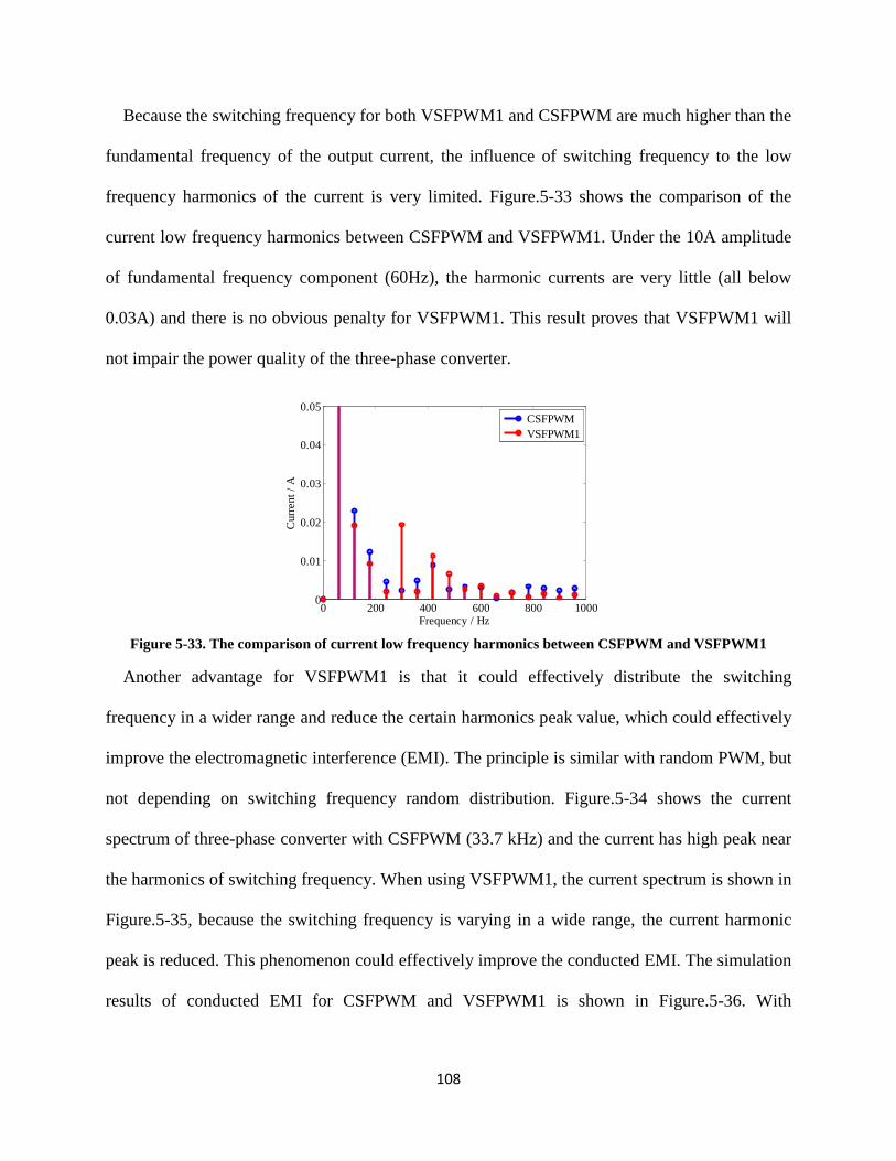
108
Because the switching frequency for both VSFPWM1 and CSFPWM are much higher than the
fundamental frequency of the output current, the influence of switching frequency to the low
frequency harmonics of the current is very limited. Figure.5-33 shows the comparison of the
current low frequency harmonics between CSFPWM and VSFPWM1. Under the 10A amplitude
of fundamental frequency component (60Hz), the harmonic currents are very little (all below
0.03A) and there is no obvious penalty for VSFPWM1. This result proves that VSFPWM1 will
not impair the power quality of the three-phase converter.
Figure 5-33. The comparison of current low frequency harmonics between CSFPWM and VSFPWM1
Another advantage for VSFPWM1 is that it could effectively distribute the switching
frequency in a wider range and reduce the certain harmonics peak value, which could effectively
improve the electromagnetic interference (EMI). The principle is similar with random PWM, but
not depending on switching frequency random distribution. Figure.5-34 shows the current
spectrum of three-phase converter with CSFPWM (33.7 kHz) and the current has high peak near
the harmonics of switching frequency. When using VSFPWM1, the current spectrum is shown in
Figure.5-35, because the switching frequency is varying in a wide range, the current harmonic
peak is reduced. This phenomenon could effectively improve the conducted EMI. The simulation
results of conducted EMI for CSFPWM and VSFPWM1 is shown in Figure.5-36. With
0 200 400 600 800 10000
0.01
0.02
0.03
0.04
0.05
Frequency / Hz
Cur
ren
t /
A
CSFPWMVSFPWM1

109
VSFPWM1, the oscillation of EMI noise is obviously reduced and an approximate 10dB
reduction of conducted EMI is expected.
Figure 5-34. Spectrum of current with CSFPWM
Figure 5-35. Spectrum of current with VSFPWM1
Figure 5-36. Simulation result: Comparison of conducted EMI for CSFPWM and VSFPWM1
For VSFPWM1, the consideration should be for all the three phases. If only keep one phase
current to be within the ripple current range, the other two phases will be impaired and make the
ripple current even worse. The simulation results of three-phase currents are shown in Figure.5-
37. Even thought the current ripple of phase-A is controlled to be constant with the range limit,
the current ripples of phase-B and phase-C are worse and exceeding the range.
0 2 4 6 8 10
x 104
0
0.1
0.2
0.3
0.4
0.5
Frequency / Hz
Cur
rent
/ A
0 2 4 6 8 10
x 104
0
0.1
0.2
0.3
0.4
0.5
Frequency / Hz
Cur
rent
/ A
104
105
106
-40
-20
0
20
40
60
80
100
120
Frequency / Hz
Cu
rre
nt
/ d
Bu
A
CSFPWMVSFPWM1

110
Figure 5-37. Three-phase current of variable switching frequency PWM only considering one phase ripple current (phase-A)
5.6 Variable Switching Frequency PWM to Control Ripple Current
RMS Value (VSFPWM2)
In many applications, the most concerned problem for current ripple is not its maximum
deviation but the long-period effects. In these applications, current requirements are usually
defined as the THD of the current and for the ripple current, its RMS value should be smaller
than a certain range.
VSFPWM1 uses the principle of re-arrangement of current ripple to meet the current ripple
requirement and could reduce the switching frequency, but for the RMS current requirement, re-
arrange the current ripple distribution could not obviously reduce the switching frequency since
the current ripple RMS value is determined by long period results.
VSFPWM2 is proposed for the application with ripple current RMS requirement for
conducted EMI improvement. Currently for conducted EMI improvement, random PWM is an
effective method. However, because random PWM methods depend on switching frequency
randomization, their influence on the RMS ripple current is not controllable. The comparison for
random PWM with CSFPWM is not fair for ripple current RMS value. VSFPWM2 is to control
0.48 0.485 0.49 0.495 0.5-15
-10
-5
0
5
10
15
time / sec
Ph
ase
curr
ent
/ A
Phase APhase BPhase C
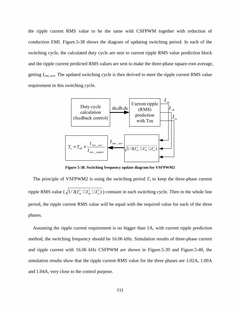
111
the ripple current RMS value to be the same with CSFPWM together with reduction of
conduction EMI. Figure.5-38 shows the diagram of updating switching period. In each of the
switching cycle, the calculated duty cycle are sent to current ripple RMS value prediction block
and the ripple current predicted RMS values are sent to make the three-phase square-root average,
getting Irms_ave. The updated switching cycle is then derived to meet the ripple current RMS value
requirement in this switching cycle.
Duty cycle
calculation
(feedback control)
Current ripple
(RMS)
prediction
with Tsn
da,db,dc
raI
rbI
rcI
requirerms
avermssNs I
ITT
_
_×=avermsI _
)(3/1 222rcrbra III ++
Figure 5-38. Switching frequency update diagram for VSFPWM2
The principle of VSFPWM2 is using the switching period Ts to keep the three-phase current
ripple RMS value ( )(3/1 222rcrbra III ++ ) constant in each switching cycle. Then in the whole line
period, the ripple current RMS value will be equal with the required value for each of the three
phases.
Assuming the ripple current requirement is no bigger than 1A, with current ripple prediction
method, the switching frequency should be 16.06 kHz. Simulation results of three-phase current
and ripple current with 16.06 kHz CSFPWM are shown in Figure.5-39 and Figure.5-40, the
simulation results show that the ripple current RMS value for the three phases are 1.02A, 1.00A
and 1.04A, very close to the control purpose.
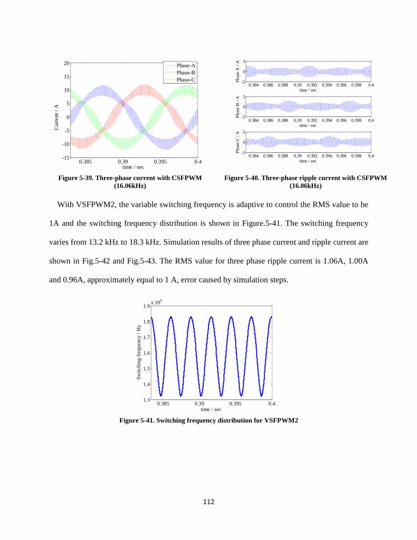
112
Figure 5-39. Three-phase current with CSFPWM (16.06kHz)
Figure 5-40. Three-phase ripple current with CSFPWM (16.06kHz)
With VSFPWM2, the variable switching frequency is adaptive to control the RMS value to be
1A and the switching frequency distribution is shown in Figure.5-41. The switching frequency
varies from 13.2 kHz to 18.3 kHz. Simulation results of three phase current and ripple current are
shown in Fig.5-42 and Fig.5-43. The RMS value for three phase ripple current is 1.06A, 1.00A
and 0.96A, approximately equal to 1 A, error caused by simulation steps.
Figure 5-41. Switching frequency distribution for VSFPWM2
0.385 0.39 0.395 0.4-15
-10
-5
0
5
10
15
20
time / sec
Cu
rre
nt /
A
Phase-APhase-BPhase-C
0.384 0.386 0.388 0.39 0.392 0.394 0.396 0.398 0.4-5
0
5
time / sec
Ph
ase
A /
A
0.384 0.386 0.388 0.39 0.392 0.394 0.396 0.398 0.4-5
0
5
time / sec
Ph
ase
B /
A
0.384 0.386 0.388 0.39 0.392 0.394 0.396 0.398 0.4-5
0
5
time / sec
Ph
ase
C /
A
0.385 0.39 0.395 0.41.3
1.4
1.5
1.6
1.7
1.8
1.9x 10⁴
time / sec
Sw
itch
ing
fre
que
ncy
/ H
z

113
Figure 5-42. Simulation results: three-phase current with VSFPWM2
Figure 5-43. Simulation results: three-phase ripple current with VSFPWM2
Because the ripple current RMS value for VSFPWM2 and CSPWM are theoretically the same,
and almost the same with the simulation results, the comparison of conducted EMI could be fair
under the ripple current requirement. The current spectrum comparison and conducted EMI
comparison are shown in Figure.5-44 and Figure.5-45. With VSFPWM2, the current spectrum
peak value is obviously reduced from CSFPWM, and the conducted EMI reduced about 10dB in
the 10kHz~5MHz range.
Figure 5-44. Comparison of current spectrum between CSFPWM and VSFPWM2
Figure 5-45. Simulation result: Comparison of conducted EMI between CSFPWM and VSFPWM2
0.385 0.39 0.395 0.4-15
-10
-5
0
5
10
15
time / sec
Pha
se c
urre
nt /
A
Phase-APhase-BPhase-C
0.384 0.386 0.388 0.39 0.392 0.394 0.396 0.398 0.4-4-2024
time / sec
Rip
ple
A /
A
0.384 0.386 0.388 0.39 0.392 0.394 0.396 0.398 0.4-4-2024
time / sec
Rip
ple
B /
A
0.384 0.386 0.388 0.39 0.392 0.394 0.396 0.398 0.4-4-2024
time / sec
Rip
ple
C /
A
0 2 4 6 8 10
x 104
0
0.2
0.4
0.6
0.8
1
Frequency / Hz
Cur
rent
/ A
CSFPWMVSFPWM2
104 105 106-20
0
20
40
60
80
100
120
Frequency / Hz
Cur
rent
/ d
BuA
CSFPWMVSFPWM2

114
5.7 Experimental Verification
In order to verify how does the theoretical ripple current prediction compare with real ripple
current in three-phase PWM converters, and to verify the performance and benefit of the
proposed VSFPWM methods, experimental testbed is build up. The testbed is a three-phase
inverter driving L-RC load, shown in Figure.5-46: L=800µH, C=25µF and R=10Ω, with 6.25
kHz switching frequency. The controller is using TMS320F28335 floating point DSP. The
switching period is updated in the interruption program. The waveforms are measured and
recorded in Tektronics DPO5204 oscilloscope with 15MHz current probe TCP303. The
hardware development will be fully discussed in chapter 7.
With R-C parallel load, the voltage drop could be treated as mainly fundamental frequency
based voltage, similar with motor back-EMF and grid voltage. If only with R load, the load
voltage would have obvious ripple component and impair the linearity of the inductor current.
Figure.5-47 shows the hardware setup, the Yokogawa oscilloscope is used to monitor the gate
voltage, the Tektronics oscilloscope is to record the main waveforms. The main circuit is put in
the isolated high power room and controlled in the low power room with remote cables.
Figure 5-46. Experimental circuit Figure 5-47. Picture of the testbed hardware

115
Picking phase-A for study for both SVPWM and DPWM, experimental results are selected
with one line cycle. With FFT analysis, the amplitude and phase-angle of the current could be
derived, and the fundamental current (average current) could be re-constructed. The comparisons
of phase current and its average value are shown in Figure.5-48 and Figure.5-49.
Figure 5-48. Experimental results: phase current and its average value with SVPWM
Figure 5-49. Experimental results: phase current and its average value with DPWM
In order to verify the proposed 7 sector and 5 sector principle of current ripple, the output
inductor voltage and corresponding phase current are shown in Figure.5-50 and Figure.5-51. The
details of 0.4ms (2.5 switching cycles) are shown in the right side of the two figures. In the
enlarged details, the sectors are very obvious. For SVPWM, 7 sectors are in one switching cycle,
for DPWM, 5 sectors are in one switching cycle. Experimental results verify the sectors
predicted ripple current variation principle.

116
0 0.002 0.004 0.006 0.008 0.01 0.012 0.014 0.016-200
0
200 V
a / V
0 0.002 0.004 0.006 0.008 0.01 0.012 0.014 0.016-200
0
200
Vb
/ V
0 0.002 0.004 0.006 0.008 0.01 0.012 0.014 0.016-200
0
200
Vc
/ V
0 0.002 0.004 0.006 0.008 0.01 0.012 0.014 0.016
-10
0
10
time / sec
Ia /
A
0.01 0.0101 0.0102 0.0103 0.0104-200
0
200
0.01 0.0101 0.0102 0.0103 0.0104-200
0
200
0.01 0.0101 0.0102 0.0103 0.0104-200
0
200
0.01 0.0101 0.0102 0.0103 0.0104-4-20246
Figure 5-50. Experimental results: phase current and corresponding inductor voltage with SVPWM
0 0.002 0.004 0.006 0.008 0.01 0.012 0.014 0.016-200
0
200
Va
/ V
0 0.002 0.004 0.006 0.008 0.01 0.012 0.014 0.016-200
0
200
Vb
/ V
0 0.002 0.004 0.006 0.008 0.01 0.012 0.014 0.016-200
0
200
Vc
/ V
0 0.002 0.004 0.006 0.008 0.01 0.012 0.014 0.016
-100
10
time / sec
Ia /
A
0.01 0.0101 0.0102 0.0103 0.0104-200
0
200
0.01 0.0101 0.0102 0.0103 0.0104-200
0
200
0.01 0.0101 0.0102 0.0103 0.0104-200
0
200
0.01 0.0101 0.0102 0.0103 0.0104-15
-10
-5
Figure 5-51. Experimental results: phase current and corresponding inductor voltage with DPWM
The error between phase current and its average value is the current ripple. The comparison
between the current ripple of experimental results and analytical predicted ripple peak are shown
in Figure.5-52 and Figure.5-53 for SVPWM and DPWM. Because of the parasitic capacitance in
the inductor, the ripple current sharp noise peak exceeds the predicted value, but still fitting well
with the predicted result. The predicted RMS current for the SVPWM is 1.04A and the
experimental result of ripple current RMS value is 1.02A; the predicted RMS current for DPWM

117
is 1.58A and the experimental result of ripple current RMS value is 1.50A. The prediction errors
are 2% for SVPWM and 5% for DPWM, mainly caused by deadtime effect, parameter non-
ideality and probe errors.
Figure 5-52. Experimental results of current ripple with SVPWM
Figure 5-53. Experimental results of current ripple with DPWM
Then the experiments are done to verify the performance of VSFPWM1. In order to achieve
2.5A range of ripple current peak value, 8.66 kHz switching frequency is used for CSFPWM, but
with VSFPWM1 the switching frequency is varying from 5.75 kHz to 8.66 kHz. The switching
frequency variation memorized in DSP is compared in Figure.5-54. The phase current and ripple
current with CSFPWM are shown in Figure.5-55 and Figure.5-56. With VSFPWM1, the phase
current and ripple current are shown in Figure.5-57 and Figure.5-58. Comparing Figure.5-55
with Figure.5-57, the three-phase current waveforms with CSFPWM and VSFPWM1 are mainly
the same. When comparing with the current ripple of the three phases, both of the two methods
could generate the current ripple within the controlled range (±2.5A), although the ripple current
of VSFPWM1 (Figure.5-58) is more dense than that of CSFPWM (Figure.5-56). The control
purpose of maximum ripple current is achieved in experiments by VSFPWM1 which reduced the
average switching frequency from 8.66 kHz to 7.3 kHz.
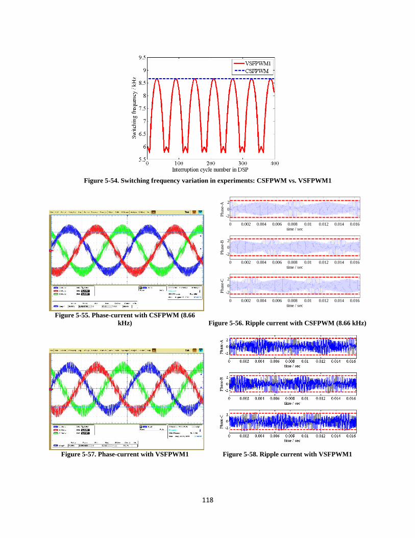
118
Figure 5-54. Switching frequency variation in experiments: CSFPWM vs. VSFPWM1
Figure 5-55. Phase-current with CSFPWM (8.66 kHz) Figure 5-56. Ripple current with CSFPWM (8.66 kHz)
Figure 5-57. Phase-current with VSFPWM1 Figure 5-58. Ripple current with VSFPWM1
0 0.002 0.004 0.006 0.008 0.01 0.012 0.014 0.016
-2
0
2
time / sec
Ph
ase-
A
0 0.002 0.004 0.006 0.008 0.01 0.012 0.014 0.016
-2
0
2
time / sec
Ph
ase-
B
0 0.002 0.004 0.006 0.008 0.01 0.012 0.014 0.016
-2
0
2
time / sec
Ph
ase-
C

119
In order to make sure using VSFPWM1 will not impair the current quality, the low order
harmonics are compared in Figure.5-59. With 9.4A fundamental current, the low order current
components are very small (less than 0.1A). With VSFPWM1, the low order harmonics are not
obviously worse than with CSFPWM. This comparison proves that with VSFPWM1, the power
quality is not impaired.
The conducted EMI of the converter is measured by an Agilent 4395A type EMI tester, with
the range from 10 kHz to 30 MHz. Experimental results are compared in Figure.5-60. The
oscillation of the EMI noise caused by harmonics of switching frequency is largely reduced by
VSFPWM1, and approximate 10 dB attenuation is achieved for VSFPWM1.
Figure 5-59. Low order harmonics comparison: CSFPWM vs.VSFPWM1
Figure 5-60. Conducted EMI comparison between
CSFPWM and VSFPWM1
Then the experiments are done to verify the performance of VSFPWM2. The RMS current is
controlled to be 1A. If using CSFPWM, the switching frequency should be 6.07 kHz, and using
VSFPWM2, the switching frequency varies from to 4.9 kHz to 7.0 kHz. The switching frequency
variation memorized in DSP is shown in Figure.5-61

120
Figure 5-61. Switching frequency variation in experiments: CSFPWM vs. VSFPWM1
The experimental results of three phase currents of CSFPWM are shown in Figure.5-62, the
ripple currents are shown in Figure.5-63. The calculated ripple current RMS values are 1.04A,
1.09A and 1.09A respectively, close to the requirement, error comes from the dead time, the
probe precision and inductance non-linearity. The experimental results of three-phase currents of
VSFPWM2 are shown in Figure.5-64, corresponding ripple currents are shown in Figure.5-65.
The calculated ripple current RMS values are 1.04, 1.09 and 1.10 respectively, which
approximately the same with CSFPWM and realizes the ripple current RMS value requirement
and could make a fair comparison with CSFPWM for conducted EMI.
Figure 5-62. Phase-current with CSFPWM ( 6.07 kHz) Figure 5-63. Ripple current with CSFPWM
(6.07kHz)

121
Figure 5-64. Phase-current with VSFPWM2 Figure 5-65. Ripple current with VSFPWM2
In order to make sure VSFPWM2 will not impair the power quality of the current, the low
order current harmonics are compared in Figure.5-66. Similar with Figure.5-59, with VSFPWM2,
the low order harmonics with VSFPWM2 is not obviously worse than CSFPWM.
Figure.5-67 shows the comparison of conducted EMI between CSFPWM and VSFPWM2.
Because of the EMI oscillation caused by harmonics of constant switching frequency is
obviously reduced by VSFPWM2, EMI is improved in med-frequency range (10 kHz to 1 MHz),
when frequency is in high frequency range, some other non-ideal factors influence the conducted
EMI and the improvement is not obvious.
Figure 5-66. Low order harmonics comparison: CSFPWM vs.VSFPWM2
Figure 5-67. Conducted EMI comparison between CSFPWM and VSFPWM2
122
5.8 Conclusions
Although random PWM as one kind of variable switching frequency PWM method for motor
drive’s power density improvement is introduced in chapter 3, this chapter aims at developing
variable switching frequency PWM methods based on current ripple analysis. First, the analytical
current ripple of three-phase PWM converter is studied and the current ripple prediction is
developed as the basis for the VSFPWM methods. Then based on this prediction, two VSFPWM
methods are proposed for losses and EMI improvement and verified by simulation and
experimental results. Following conclusions could be made:
1. With each of the voltage vector, the output current slope is constant. Based on the 8
voltage vectors in the converter, 8 Thevenin equivalent circuits are modeled to derive the
current ripple with each vector. The current ripple slope is summarized in Table.1.
2. With SVPWM and DPWM, there are 7 and 5 sectors of current ripple in each of the
switching cycle, which is determined by the duty cycles of each phase. Then the current
ripple and its peak value and RMS value could be predicted for the whole line period.
Simulation and experimental results show that the prediction is precise. In experiment,
the non-linearity of the inductance and deadtime could bring a little difference.
3. DPWM has obviously bigger ripple peak value and RMS value than SVPWM for the
same condition, although the switching losses are effectively reduced.
4. For SVPWM and DPWM, there are 7 and 5 ripple current sectors in each switching cycle
in the output phase current, the ripple current value is determined by the switching period
length, duty cycle of three-phase, DC-link voltage and output inductor. Based on part I of
the two papers, the ripple current in each switching period could be predicted before the
pulses are generated.
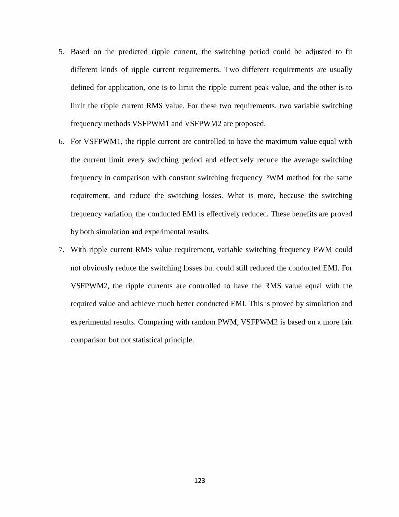
123
5. Based on the predicted ripple current, the switching period could be adjusted to fit
different kinds of ripple current requirements. Two different requirements are usually
defined for application, one is to limit the ripple current peak value, and the other is to
limit the ripple current RMS value. For these two requirements, two variable switching
frequency methods VSFPWM1 and VSFPWM2 are proposed.
6. For VSFPWM1, the ripple current are controlled to have the maximum value equal with
the current limit every switching period and effectively reduce the average switching
frequency in comparison with constant switching frequency PWM method for the same
requirement, and reduce the switching losses. What is more, because the switching
frequency variation, the conducted EMI is effectively reduced. These benefits are proved
by both simulation and experimental results.
7. With ripple current RMS value requirement, variable switching frequency PWM could
not obviously reduce the switching losses but could still reduced the conducted EMI. For
VSFPWM2, the ripple currents are controlled to have the RMS value equal with the
required value and achieve much better conducted EMI. This is proved by simulation and
experimental results. Comparing with random PWM, VSFPWM2 is based on a more fair
comparison but not statistical principle.

124
Chapter 6. Permanent Magnet Motor Control with
High Density Motor Drive
This chapter mainly deals with the permanent magnet (PM) motor control issues of the high
density motor drive. This chapter starts with an introduction to the fundamental knowledge and
the state-of-the-art of PM machine and high performance AC motor control. Then a speed
sensorless control method is introduced in 6.2. The start-up transient problem of sensorless
control in high density motor drive is studied and an improved start-up process is proposed in 6.3.
With the improved start-up process, experiments are introduced in 6.4 and the conclusions are
summarized in 6.5.
6.1 Introduction
Before power electronics motor drives were widely applied motion control system, DC motors
with mechanical brushes had been popular because of their simple current-torque and voltage-
speed relationships. Since 1970s, high performance AC motor control methods have been
developed rapidly together with power electronics devices, making the high performance control
of AC motor be as easy as DC motor control and could avoid using the mechanical brushes.
Typically there are two main groups of AC motor control methods with motor drives: vector
control and direct torque control (DTC)[48]. Vector control, or called field oriented control (FOC)
aims at orienting the current and flux in synchronous rotating d-q axis and achieving decoupled
d-q control and with simple torque-current relationship. DTC deals with the stationary D-Q axis
and control the flux and torque of the motor to constrain to reference value with different voltage
vectors. Both of vector control and DTC can achieve fast dynamic response for AC motor and

125
become widely applied in modern motor drives. Comparing with DTC, vector control is more
popular in applications. In this chapter, vector control is applied to the motor drive.
With both vector control and DTC, in order to control the motor speed, real motor speed
should be fed back to the controller for speed regulation. For vector control, in order to transfer
the three-phase AC value to d-q axis, rotor position is required, too. Conventional position/speed
sensor for motor increases the system complexity and cost and reduces the system reliability.
Speed/position sensorless control methods developed in the recent 30 years, aiming at estimating
the rotor speed and position by using the voltage and current information and eliminating the
mechanical sensors. Among the sensorless control methods, two main groups can be ascribed:
the methods based on fundamental wave model and the methods based on harmonics model[50].
The methods based on harmonic model require extra signal injection from the motor drive and
derive the speed and position information from the harmonics in the motor, they usually require
asymmetry in the motor structure and bring more noises and losses, but they could work well at
low speed and can be worked at start-up process. The methods based on fundamental wave
model do not need extra signal injection and special motor structure, but they could not work
well at low speed and could not work for start-up process. In this chapter, a fundamental wave
based sensorless control method is applied in the load motor.
Among all the AC motors, permanent magnet synchronous motors (PMSM) developed since
1950s could achieve high power density especially with high energy density permanent magnetic
materials [49]. PMSM is widely applied in high performance motion control area and could be a
good control object for high density high efficiency motor drive application. Based on the flux
directions, PMSMs could be ascribed to two main groups: radial flux PM motors with flux
direction along the radius of the motor and the axial flux PM (AFPM) motors with flux direction

126
paralleling with the motor shaft. AFPM motor has been studied for application in several areas[73].
The machine topology has many attractive characteristics like high efficiency and superior
torque density. With its pan-cake structure, it can be easily applied in fan-type of load. In recent
years, new technologies were used in AFPM motor such like slotless-type motor and coreless-
type motor. This kind of motors exhibits low inductance because of their large effective air-gap
length. From the view of motor control, the AFPM motor is basically equivalent to the normal
radial-flux surface mounted PM motor. In this chapter two different AFPM motors are used as
load motor, one with slot and the other is slotless AFPM motor with PCB windings.
Research have been done for PM motor’s sensorless control. However, for high density motor
drives with small DC-link capacitor and non-regenerative active front-end rectifier, how could
sensorless control work is uncertain. The DC-link capacitor is designed with little energy storage
for dynamic transient compensation, for fan-type of load with little dynamic transient. However,
with sensorless control based on fundamental wave model, the start-up process should used non-
sensorless control, there is a switching transient to sensorless control, how will the transient
influence the motor drive and the solution is studied in this chapter.
6.2 Speed sensorless control method for PM motor
In order to achieve speed sensorless vector control for PM motor, the mathematical model of
PM motor is studied at first. In this chapter, the PM motor is with low saliency and the d-q
inductance is equal to Ls; the stator resistance is Rs; the PM flux is mλ ; rotor pole pairs is p; the
d-q voltage and current are vd, vq and id, iq and the electromagnetic torque is Te. Figure.6-1
shows the coordinate transformation in the PM motor. With park transformation[48] (shown in (6-
1)) the voltage and the current in a-b-c coordinate could be transferred to the rotating d-q

127
coordinate and the AC values are transferred to be DC values. In d-q coordinate the voltage
equations are shown in (6-2) and the torque equation is shown in (6-3).
rθ
Figure 6-1. Coordinate transformation in PMSM
+−−−−+−
=)3/2sin(),3/2sin(,sin
)3/2cos(),3/2cos(,cos
3
2πθπθθπθπθθ
rrr
rrrT (6-1)
+++=
−+=
mrqssrqssqssqs
qssrdssdssds
iLidt
dLiRv
iLidt
dLiRv
λωω
ω (6-2)
qme ip
T λ2
3= (6-3)
The sensorless vector control diagram of PM motor is shown in Figure.6-2. The out-loop of
the controller is the speed loop with a speed regulator. The output of the speed regulator is the
reference q-axis current. The inner loop of the controller is the d-q current loop with d-q
decoupling regulator, the output of the current regulator is the duty cycle in d-q axis. Then the

128
duty-cycle is combined in space vector modulation module and the PWM signals are sent to the
inverter.
rdiˆ
rqiˆ
rθ
rω
refω
refdi _
decouplingqv _
decouplingdv _
rωrefqi _
rqiˆ
rdiˆ
rqv ˆ
rdvˆ
Figure 6-2. Sensorless vector control diagram for PM motor
In Figure.6-2, the feedback speed rω and rotor electrical angle rθ are estimated by the
sensorless module. The sensorless control is based on the back-EMF observer shown in Figure.6-
3. The input vector u is the d-q voltage [vd,vq]’, state variable x is d-q current and back-EMF
vector [id,iq,ed,eq]’ and the output vector y is [id,iq]’. The state variable function BuAxx +=& is
shown in (6-4). With a designed gain matrix L, the observer is designed to generate observed
vectorx , containing the estimated back-EMF qde ,ˆ , shown in (6-5). Then using a PI regulator to
control 0ˆ =de and generate estimated speed ω , its integral is the estimated rotor position θ ,
shown in Figure.6-4.

129
Figure 6-3. Back-EMF observer structure [51][52]
Figure 6-4. Position/speed tracking module [51][52]
+
−−
−
=
q
d
s
s
q
d
q
d
ss
s
ss
s
q
d
q
d
v
v
L
L
e
e
i
i
LL
R
LL
R
e
e
i
i
0,0
0,0
1,0
0,1
0,0,0,0
0,0,0,0
1,0,,ˆ
0,1
,ˆ,
ω
ω
&
&
&
&
(6-4)
)ˆ(ˆˆ xCyLBuxAx −++=& (6-5)
Reference [51] and [52] present the mathematical model of PM motor’s sensorless control and
the speed controller and current controller are designed in frequency domain. With sensorless
control, current loop is designed to be 400Hz and the speed loop is designed with 3 Hz
bandwidth.
In the experiments, the motor drive system is shown in Figure.6-5. It contains a Vienna-type
rectifier in the AC side and a two-level VSI in the motor side. The motor drive is built with SiC
JFETs and SiC SBDs to achieve high switching frequency. For high density motor drive in the
experiments, the DC-link capacitor is designed to be 17.5µF.

130
The motor is connected to the load generator driven by a back-to-back commercial Yaskawa
motor drive. The load torque can be controlled with constant value. The motor testbed pictures
are shown in Figure.6-6, with AFPM motor with slot and without slot (PCB motor). The
parameters of the motor drives are shown in Table.6-1. The first motor is with slots in the stator
and the weight is heavier than the second motor without slots (PCB motor).
Figure 6-5. Diagram of the experimental platform
(a) (b)
Figure 6-6. Experimental testbed: (a) AFPM motor with slots, (b) Slotless AFPM motor with PCB
windings

131
Table 6-1. Parameters of the two AFPM motors in the experiments
Motor 1: AFPM motor with slots Motor 2: PCB motor
Rs (Ω) 0.53 0.8
Ls ( Hµ ) 280 30
PM flux (Wb) 0.0347 0.0261
Pole pairs 6 6
Rated speed (rpm) 15000 18000
Rated torque (Nm) 6.2 4.7
The mathematical model and control algorithms are similar for the two motors, the main
difference is that the stator inductance of the second motor is much lower than the first motor. In
the experiments a three-phase series inductor is used to attenuate the current ripple of the second
motor. Experiments are done for both motors to verify the control methods.
6.3 Improvement for start-up transient
The proposed sensorless control method depends on the back-EMF observing, which means
the performance will be poor at low speeds. Thus non-sensorless control methods are used when
the motor is in its start-up process, then the motor will be switched to sensorless mode. The
normal starting process is shown in Figure.6-7.
(1) In Region 1, by injecting DC current, the motor is aligned to the zero angle position.
(2) In Region 2, the speed increases continuously, but the observer cannot work well, so the
reference currents id_ref and iq_ref are given directly and rotated with the open loop speed.
(3) In Region3, the observer begins to work, generatingdqi ,ω andθ , but the motor is still driven

132
without closing speed loop.
(4) When the reference speed is approaching ωplug, the observer estimated ω and θ will be
stable, at t3, estimated position θ replaces the open loop position and estimated speed ω is
plugged into the speed loop, the motor goes into sensorless mode in Region 4.
(5) In Region 5, the reference speed reaches the given value ωref.
1t 2t 3t 4t
observerω
plugω
refω
Figure 6-6. Conventional start-up process for PMSM for sensorless control
At time t3, because of the sudden plug in, a transient appears and the DC bus voltage oscillates.
A low voltage and low speed experiment has been done for Motor 1 under 90V DC voltage. The
experimental result is shown in Figure.6-7, in which the transient peak in the DC voltage is
V20± .
Figure 6-7. DC link voltage at the switching point with conventional start-up process
0.01 0.02 0.03 0.04 0.05 0.06
70
80
90
100
110
120
Time / sec
Vdc
/ V

133
There are two main reasons for the transient at the sensorless plug-in time.
First of all, as discussed in section II, in Region 1 and Region 2, the motor is driven with given
reference current vector , and the rotating speed of the vector is directly
given by reference speed ωref, which means the reference angle is ∫= dtrefref ωθ . However, as the
reference current is directly given and not based on the load torque requirement, the real rotor
will not be in the reference d-q coordinate. This means that if the observer works well, the
estimated rotor angle is θest ≠θref. This principle is shown in Figure.6-8. With the same current
vector iv
in Region 3, the feedback current and the observer current will be in different
coordinates. This phenomenon is proved by experimental result in Figure.6-9. In time t3, θest will
replace θref, which will cause significant transient in the motor. In addition, the power balance
between the rectifier and the inverter will be disturbed, causing the DC bus voltage to oscillate.
fdbdi _
fdbqi _
obsqi _
obsdi _
iv
errθ
Figure 6-8. Current vector relationship in open loop and observer coordinate
Figure 6-9. Rotor angle in open loop and observer
refqrefdref ijii __ ⋅+=v
0.01 0.02 0.03 0.04 0.05 0.06-4
-2
0
2
4
Time / sec
Ro
tor a
ngle
rad
In reference coordianteIn observer coordinate

134
The other reason for transient is shown in Figure.6-10. Before t3, iq_ref is directly given to drive
the motor (iq_ref0), at t3, iq_ref is suddenly switched from iq_ref0 to the output of the speed PI
regulator. The experimental result in Figure.6-11 proves this phenomenon: at the switch point,
iq_ref jumps directly from 4A to less than 0, and feedback current iq_fdb tracks iq_ref and breaks the
power balance, causing the DC bus voltage oscillation.
Figure 6-10. iq_ref sudden change in speed loop plug in time
Figure 6-11. Experiment result of iq_ref sudden change in the plug in time (t3): Top: q-axis current, Bottom: DC bus voltage
Based on the results of the analysis, an improved start-up process is proposed, shown in
Figure.6-12 and Table.6-2. This process contains seven regions. Building on with the original
process in Figure.6.6, two new regions are added in the start-up process.
refωObsω
refqi _
0_refqi
0.01 0.02 0.03 0.04 0.05 0.06-2
0
2
4
6
Iq /
A
0.01 0.02 0.03 0.04 0.05 0.0660
80
100
120
Time / sec
Vd
c / V
IqrefIqfdb

135
1t 2t 3t 4t
observerω
plugωrefω
Region 1 Region 2 Region 3 Region 4
Speed
Time
Region 5
5t 6t
Region 6
calculateωtrackω
Region 7
Initial alignment
Open loop start,
observer done not
work
Observer begins to
work
Calculate the
updated iq_ref
Adjust iq_ref, set speed
regulator initial value
Switch to sensorless
control
Arrive at reference
speed
Figure 6-12. Proposed start-up process of sensorless controlled PM motor
Table 6-2. Function of each region in the proposed start-up process
Region 1 Initial alignment
Region 2 Open-loop start-up,
observer does not work
Region 3 Observer begins to work
Region 4 Calculate the updated
iq_ref
Region 5 Adjusts iq_ref
Region 6 Switch to sensorless
control
Region 7 Arrive at reference speed
In order to reduce the angle error in the open-loop accelerating time as much as possible, an
updated iq_ref is calculated in Region 4. The calculated method is based on a sample of 1000 data
points of iq_Obs in the beginning of Region 4. An average is calculated, and multiplied by a
coefficient λ (λ >1), shown in (6-6). If Iqref_update is applied to the q-axis, it will be near the actual

136
torque current, so θerr will be much smaller. The reason to multiply λ is to make sure the current
is big enough to accelerate the motor. In this experiment, λ=1.2. In Region 5, the reference
current iq_ref is gradually adjusted to Iqref_update with a slope. Experimental results are shown in
Figure.6-13, where we see that in 0.1 second the feedback q-axis current gradually tracks the
reference current to the updated value, and the DC bus voltage stays nearly constant in this
period. Then the iq in two different coordinates will be nearly the same, and the rotor position
will be tracked to near the reference coordinate, experimental results are shown in Figure.6-14.
λ×= ∑ )1000
1(
1000
1__ Obsqupdateqref II (6-6)
In addition, the calculated Iqref_update is also sent to the speed PI controller in Region 5 as the
initial value, so that when the sensorless control is plugged in at t5, the reference current will not
suddenly drop. The experimental result is shown in Figure.6-15. If the initial value is not settled,
iq_ref will jump more than 3A. If the initial value is settled, iq_ref jump in t5 is less than 0.5A.
Figure 6-13. Experimental results: reference and feedback q-axis current and DC bus voltage in the tracking period (t4)
0.02 0.04 0.06 0.08 0.1 0.12 0.14 0.16 0.181
2
3
4
5
Iq A
0.02 0.04 0.06 0.08 0.1 0.12 0.14 0.16 0.1886
88
90
92
94
Time / sec
Vdc V
Reference IqFeedback Iq

137
Figure 6-14. Iq and rotor angle in open loop and observer coordinates: In Region 5, after Iq_ref tracking
Figure 6-15. Iq_ref in the sensorless plug in time (t5): With and without speed PI initialization
A final comparison of experimental results is made in Figure.6-16. With the normal method
(method 1), the peak transient DC bus voltage will be V20± . With iq_ref adjustment in Region 5
(method 2), the peak transient DC bus voltage will be weakened to V15± .With iq_ref adjusted and
speed PI initialization (method 3), the peak transient DC bus voltage will be less thanV5± . The
proposed start-up process can obviously improve the transient.
0.01 0.02 0.03 0.04 0.05 0.060
2
4
Iq A
0.01 0.02 0.03 0.04 0.05 0.06-4-2
0246
Time / sec
Ro
tor
an
gle
rad
In reference coordinateIn observer coordinate
In reference coordinateIn observer coordinate
0.01 0.02 0.03 0.04 0.05 0.06-1
-0.5
0
0.5
1
1.5
2
2.5
3
3.5
Time / sec
Iqre
f / A
Without Speed PI initialization With Speed PI initiallization

138
Figure 6-16. DC bus voltage in transient with different methods
The start-up improvement experiments have also been done in the PCB motor, showing the
similar results.
6.4 Experiments
When the DC-link voltage is pushed to high value, this transient in the DC-link will force the
DC-voltage protection to shut-down the motor drive. With the improved start-up process, the
high power and high voltage performance can be achieved. In 6.4, 330V DC-link voltage is
added to both Motor 1 and Motor 2 to study the high power performance of the motors.
Based on the experimental testbed in Figure.6.5, the load generator back-to-back converter is
set with torque limit and works as a constant torque load. The controlled AFPM motors are
started with the improved start-up process and finally reach the rated speed.
For Motor 1, Figure.6-17 and Figure.6-18 are the experimental results using 330V DC-link
voltage with the motor speed pushed to 5500rpm with sensorless control. Figure.6-17 is the
0.01 0.02 0.03 0.04 0.05 0.06
70
80
90
100
110
120
Time / sec
Vd
c / V
Method 1Method 2Method 3
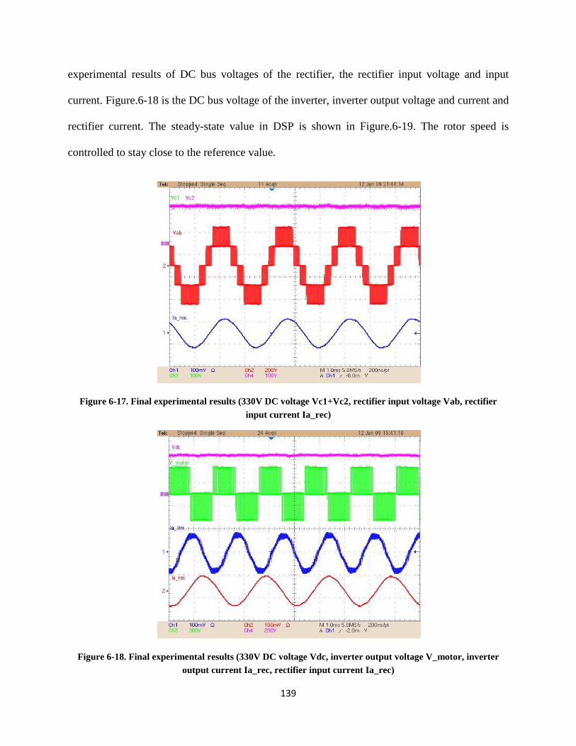
139
experimental results of DC bus voltages of the rectifier, the rectifier input voltage and input
current. Figure.6-18 is the DC bus voltage of the inverter, inverter output voltage and current and
rectifier current. The steady-state value in DSP is shown in Figure.6-19. The rotor speed is
controlled to stay close to the reference value.
Figure 6-17. Final experimental results (330V DC voltage Vc1+Vc2, rectifier input voltage Vab, rectifier input current Ia_rec)
Figure 6-18. Final experimental results (330V DC voltage Vdc, inverter output voltage V_motor, inverter output current Ia_rec, rectifier input current Ia_r ec)
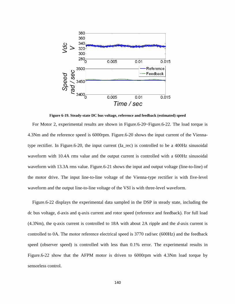
140
Figure 6-19. Steady-state DC bus voltage, reference and feedback (estimated) speed
For Motor 2, experimental results are shown in Figure.6-20~Figure.6-22. The load torque is
4.3Nm and the reference speed is 6000rpm. Figure.6-20 shows the input current of the Vienna-
type rectifier. In Figure.6-20, the input current (Ia_rec) is controlled to be a 400Hz sinusoidal
waveform with 10.4A rms value and the output current is controlled with a 600Hz sinusoidal
waveform with 13.3A rms value. Figure.6-21 shows the input and output voltage (line-to-line) of
the motor drive. The input line-to-line voltage of the Vienna-type rectifier is with five-level
waveform and the output line-to-line voltage of the VSI is with three-level waveform.
Figure.6-22 displays the experimental data sampled in the DSP in steady state, including the
dc bus voltage, d-axis and q-axis current and rotor speed (reference and feedback). For full load
(4.3Nm), the q-axis current is controlled to 18A with about 2A ripple and the d-axis current is
controlled to 0A. The motor reference electrical speed is 3770 rad/sec (600Hz) and the feedback
speed (observer speed) is controlled with less than 0.1% error. The experimental results in
Figure.6-22 show that the AFPM motor is driven to 6000rpm with 4.3Nm load torque by
sensorless control.

141
Figure 6-20. Rectifier current, inverter current and DC-link voltage of the motor drive with 330V dc voltage,
6000rpm and 4.3Nm load torque for Motor 2
Figure 6-21. Steady state waveform of the converter with 330V dc voltage, 6000rpm and 4.3Nm load torque
(Current probes use 500mA/10mV ratio transformation to the oscilloscope)

142
Figure 6-22. Steady-state waveform of the converter with 330V DC voltage, 6000rpm speed and 4.3Nm load
torque: data sampled in DSP
6.5 Conclusions
Motor control is the final performance verification of the high density motor drive. This
chapter introduces an experimental testbed for testing the performance of a novel SiC devices-
based AC-DC-AC motor drive with a Vienna-type rectifier and a VSI structure. The testbed
contains the AC-DC-AC motor drive, the controller, and two kinds of AFPM motors as control
objects. The load machine is driven by a commercial back-to-back motor drive so the power can
be fed back to the grid and the load torque can be controlled.
Since the back-EMF observer based sensorless control method cannot work well at low speeds,
it needs to be started with open-loop control then switched to sensorless control. There is a
significant transient in the dc bus voltage at the switching time. This transient triggers the dc bus
protection and makes the system stop working. This transient is even worse in Vienna-type non-
regenerative rectifier. The reason for this transient is as follows:
0.01 0.02 0.03 0.04 0.05 0.06
320
340
360
Vd
cV
0.01 0.02 0.03 0.04 0.05 0.06
-2
0
2Id A
0.01 0.02 0.03 0.04 0.05 0.06
16
18
20
Iq A
0.01 0.02 0.03 0.04 0.05 0.063760
3770
3780
time / sec
Sp
eed
rad/
sec
ReferenceFeedback

143
(1) Since the reference current is directly given and different from the load-required current,
there will be an error between the open-loop rotor angle and observed rotor angle, the
sudden change of the angle can cause a transient.
(2) At the switching time, the reference q-axis current is suddenly changed from the open-
loop value to 0, which also causes an obvious transient.
Based on these reasons, an improved start-up method is applied by linearly adjusting the
reference current in open loop control and initializing the speed regulator. Experimental results
show that with the improved start-up method, the transient problem is solved.
With these methods, the AC-DC-AC motor drive can control the two AFPM motors to high
speed with 4.3Nm load torque under 330V DC-link voltage. Experimental results show that in
steady-state dc bus voltage is controlled with less than 1% error, the speed is controlled with less
than 0.1% error and the input and output current are sinusoidal with low harmonics since the
switching frequency can be high.

144
Chapter 7. Modular Motor Drive Design and
Development
This chapter introduces the hardware design examples of high density and high efficient motor
drives with the technologies developed in this dissertation. The design method is based on
modular design techniques which have good tolerance and easy implementations. In 7.1, the
modular design technique is briefly introduced with the example of a 10kW AC-DC-AC motor
drive with SiC devices. Then the design example of 30kW DC-fed motor drives with Si IGBTs is
discussed. In 7.2 the system configuration and interface are introduced. In 7.3, hardware design
and construction is introduced. In 7.4, different versions of phase-leg modules are compared. In
7.5, full power test of the designed modular converter is tested and compared with design results.
The conclusions are made in 7.6.
7.1 Introduction
Hardware development of high density motor drive is presented in this chapter. Engineering
design of the motor drive should be programmable and be easy to update with new device
packages. The development of the motor drive is based on modular design strategy is applied for
the motor drive. For example, for the motor drive designed with customized high temperature
package devices, the first version of the motor drive is build up with commercial device based
phase-leg module and assembled to be the motor drive. The circuit and motor control function
could be verified in this motor drive. Then the phase-leg module is updated with customized
package devices based phase-leg module, with the same interface with the converter. This
approach could highly simplify the development of the motor drive hardware implementation.

145
The development of 10kW AC-DC-AC motor drive with SiC devices is introduced by
reference [1] and [26]. The converter topology is show in Figure.7-1. There are two versions of
the motor drive: with commercial devices based phase-leg and with high temperature package
devices based phase-leg module. Figure.7-2 and Figure.7-3 show the phase-leg module of
version 1 and version 2. The phase-leg modules for the two versions have the same power
terminals and the same signal terminals, which can connected to the mother board shown in
Figure.7-4. The control and protection functions of the motor drive are the same and the only
difference is the phase-leg module. Then the development of the motor drive could be
concurrently realized in phase-leg module and control/protection.
M
AC
AC
AC
L in C1
C2
Figure 7-1. Three-phase AC-fed motor drive with SiC devices
Figure 7-2. Version1 phase-leg module(with commercial devices): rectifier (left); inverter (right)

146
Figure 7-3. Version 2 phase-leg module (with customized package devices): rectifier (left); inverter (right)
Figure 7-4. Mother board of the 10kW AC-DC-AC motor drive
The development of the high density AC-fed motor drive based on SiC devices for aircraft
application is introduced in reference [1]. The work of Chapter 2 is applied for this motor drive;
the work of Chapter 3 and Chapter 6 are based on this hardware testbed. In this chapter, the
modular design method is applied to a 30kW DC-fed motor drive with Si IGBTs for electrical
vehicle application. The experiments for Chapter 4 and Chapter 5 are based on this testbed.
7.2 System configuration and interface
The DC-fed modular motor drive architecture is shown in Figure.7-5. The center of the system
is the mother board, which process both the power and signals. The carrier board serves as the

147
interface between the controller and the mother board. The sensor signals from the mother board
are proceeded in the carrier board and feedback to the DSP controller AD channels; the PWM
signals from the DSP controller are proceeded in the carrier board and sent to the mother board.
In order to simulate the case in vehicle, 12V DC power performs as the input control power, all
the control and gate driver power are generated from the 12V DC power in the carrier board. N
phase-leg modules are connected to their driver boards and connected to the mother board, with
interface of power terminals, gate driver terminals and signal terminals. Power conversion is
realized in each module and the DC input power is converter to the AC output power.
Figure 7-5. the system architecture of the modular motor drive
With the system configuration and interface in Figure.7-5, the modular motor drive could be
developed with different topologies. Two main groups of topologies based on modular motor
drive structure are shown in Figure.7-6[87]. Figure.7-6 (a) is based on N-phase half-bridge
structure, which needs N phase-leg modules; Figure.7-6(b) is based on N-phase full-bridge
structure, which needs 2N phase-leg modules. Both the two structures could be implemented

148
with the architecture in Figure.7-5. For the full-bridge structure, each phase winding could be
controlled independently and the fault-tolerant redundancy of the motor drive could be higher,
but the weight of the motor drive will be higher and the efficiency will be lower. In this chapter,
three-phase inverter based on half-bridge structure is build up with the modular architecture in
Figure.7-5.
. . . MotorPhase 1
Phase 2 Phase
N
(a) Half bridge structure
. . .Winding 1 Winding N
(b) Full bridge structure
Figure 7-6. Two kinds of different topologies for modular motor drive
For hardware development convenience, the power and signal terminals are usually designed
with plug-and-play structure but not soldering. It will be easier for hardware update and repairing.
The power interface is using screw hard connection to make it solid, the signal interface is using
soft cable connection to make it flexible.
7.3 Hardware design and construction
The core idea of modular design method is separating the development of each part
independently. Based on the structure of Figure.7-5, the development of the DC-fed motor drive
is arranged as three main parts: controller, mother board and phase-leg modules. The
development of phase-leg module is the key part for converter update. The design procedure is
shown in Figure.7-7. After the development of each part, the converter is assembled and tested to
evaluate the system performance.

149
Figure 7-7. Design procedure for modular motor drive
The hardware design of phase-leg module is through an error-debugging process. After the
design of phase-leg module, it is evaluated with electrical test first, mainly with double-pulse-test
to test the switching performance. After the test the switching performance and losses are
evaluated and the problems could be found, and used as the guidance for update of the phase-leg
module. The controller and mother board hardware is kept the same in the development, and
three different versions of phase-leg modules are developed. The controller design contains the
hardware (interface board) design and software design.
7.3.1 Controller
Float point DSP has obvious advantages over fix-point DSP including more precise output and
easier development of the code[55]. Reference [86] introduces a “universal controller” based on
Shark series floating point DSP, however, it has no on-chip PWM function and the PWM
waveform are realized in an extra FPGA, also the main-frequency of the DSP is 80MHz, limited

150
the calculation. Texas interment developed the first series of float DSP for power electronics
control: the TMS320F28XXX series. The TMS320F28335 (150MHz) has 12 on-chip PWM
terminals and 12 bits on-chip AD channels. The EVM board of this DSP also has on-board
emulator. This EVM board is selected as the controller for the modular motor drive. However,
the EVM board only provides the pin-terminals of the chip. Both the analog and digital signals
need process before connected to the mother board, which are realized in the carrier board.
Figure.7-8 shows the interface between the DSP board and the mother board through the carrier
board. The mechanical support of the DSP board is by the connecting pins between the carrier
board and the DSP board. PWM signals are transferred from 0-3.3V to 0-5V with protection in
the carrier board with buffers and sent to the mother board, the analog signals are transferred to
the range of the AD channel (0-3V) in the carrier board and sent to the DSP board, the analog
signal process circuit also works as analog filter. The photo of the real controller board and
carrier board is shown in Figure.7-9.
Carrier Board
DSP Board
Mother board
Analog signals, button signals
PWM signalscommand
Sensor signals
PWM signals, gate power
Figure 7-8. The interface between the controller and the mother board

151
Figure 7-9. Photo of DSP controller with the carrier board
7.3.2 Mother board
The mother board serves as the key interface for all the power components. The power
terminals of the mother board contains the DC power input and AC output; the signal terminal
contains the 50 pins connection from the carrier board and 3 gate driver terminals to the three
phase leg modules. The mother board contains four voltage sensors (DC link voltage and three
line-to-line voltages) by analog circuit and three current sensors by LEM HAS-100.
Design of DC-link capacitor mainly deals with two factors: the energy storage and decoupling.
DC-link capacitor mainly consists of two types: the electrolytic capacitor and film capacitors.
Electrolytic capacitor could be designed with high capacitance, but has big equivalent series
inductance (ESL) which performs badly in high frequency range, it could serves as the energy
storage capacitor. Film capacitor for the DC link usually has capacitance less than 1 µF, but has
good high frequency performance; it could serves as the decoupling capacitors. For the modular
motor drive, 6 electrolytic capacitors (1000µF, 450V, 0ALC40C102FL450) are connected as a
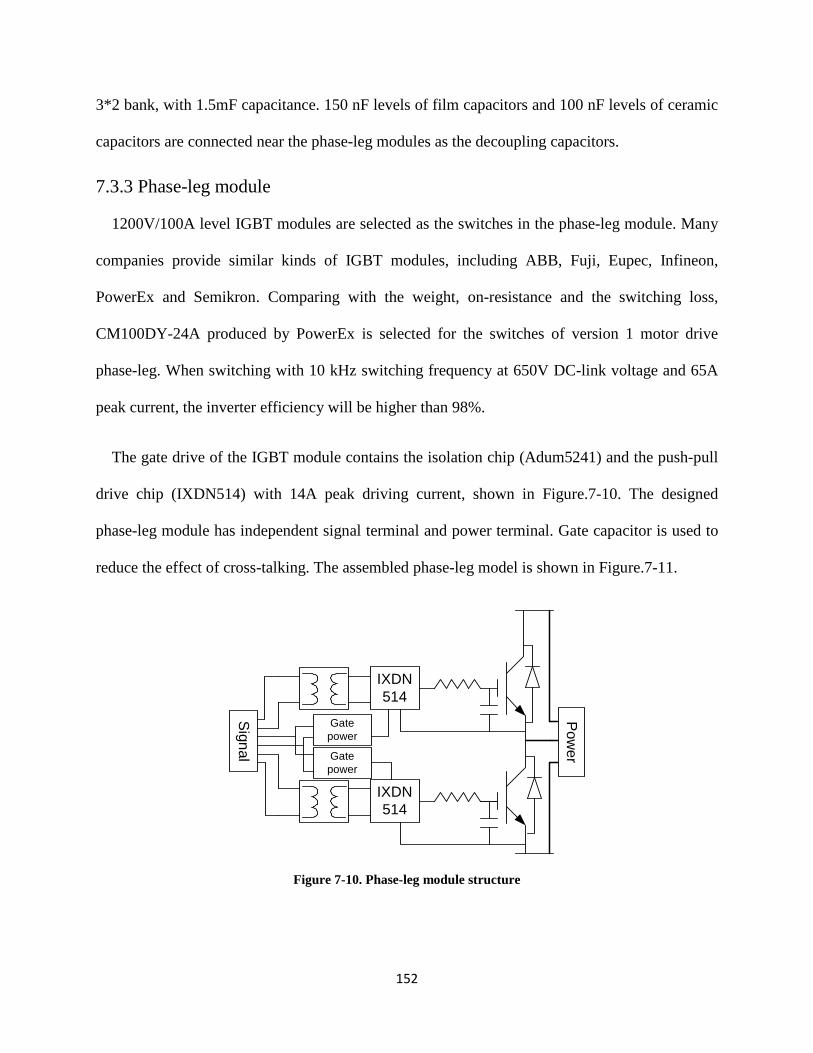
152
3*2 bank, with 1.5mF capacitance. 150 nF levels of film capacitors and 100 nF levels of ceramic
capacitors are connected near the phase-leg modules as the decoupling capacitors.
7.3.3 Phase-leg module
1200V/100A level IGBT modules are selected as the switches in the phase-leg module. Many
companies provide similar kinds of IGBT modules, including ABB, Fuji, Eupec, Infineon,
PowerEx and Semikron. Comparing with the weight, on-resistance and the switching loss,
CM100DY-24A produced by PowerEx is selected for the switches of version 1 motor drive
phase-leg. When switching with 10 kHz switching frequency at 650V DC-link voltage and 65A
peak current, the inverter efficiency will be higher than 98%.
The gate drive of the IGBT module contains the isolation chip (Adum5241) and the push-pull
drive chip (IXDN514) with 14A peak driving current, shown in Figure.7-10. The designed
phase-leg module has independent signal terminal and power terminal. Gate capacitor is used to
reduce the effect of cross-talking. The assembled phase-leg model is shown in Figure.7-11.
IXDN514
IXDN514
Signal
Pow
er
Gate power
Gate power
Figure 7-10. Phase-leg module structure
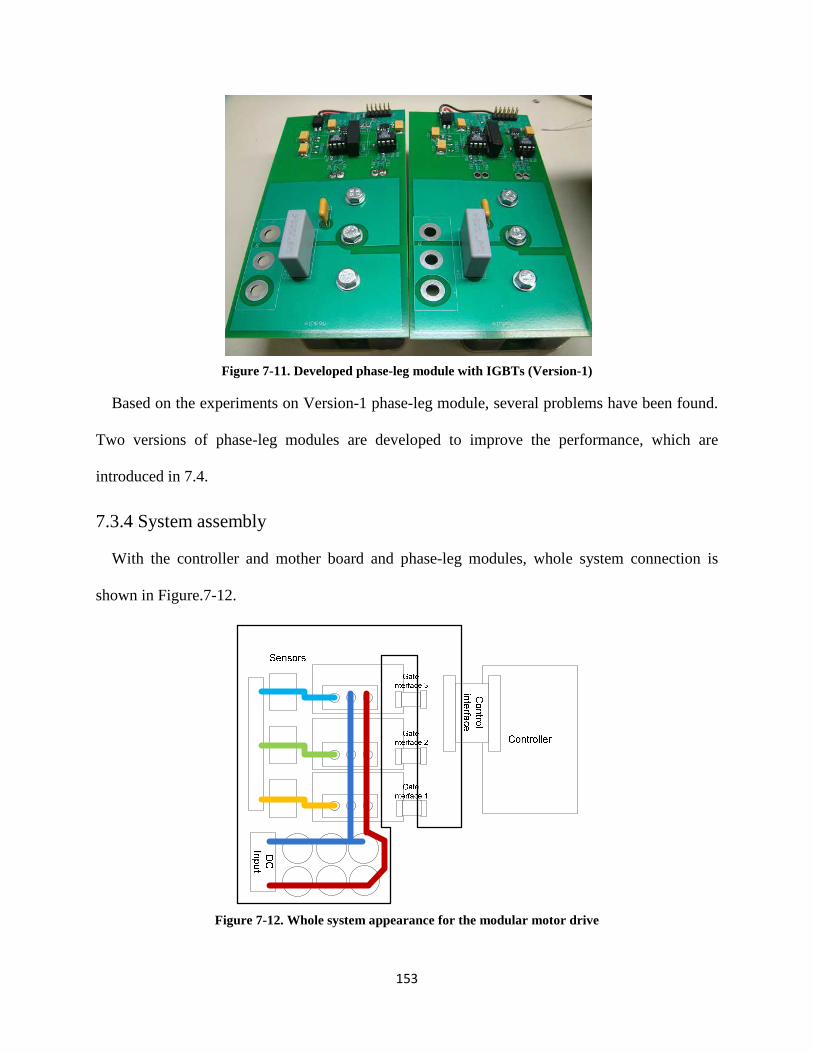
153
Figure 7-11. Developed phase-leg module with IGBTs (Version-1)
Based on the experiments on Version-1 phase-leg module, several problems have been found.
Two versions of phase-leg modules are developed to improve the performance, which are
introduced in 7.4.
7.3.4 System assembly
With the controller and mother board and phase-leg modules, whole system connection is
shown in Figure.7-12.
Figure 7-12. Whole system appearance for the modular motor drive

154
For converter cooling, air-cooling and liquid cooling are two typical kinds of methods. Liquid
cooling system is applied for the three-phase leg modules, the module distribution is show in
Figure.7-13.
224mm
142m
m48mm
94mm
48mm 48mm
Figure 7-13. Three phase-leg modules on the liquid cooling plate
The main components weight estimation is shown in Table.7-1. The estimated weight for the
motor drive is 4.6kg, which means the density of the 30kW motor drive is 6.4kW/kg.
Table 7-1. Main components weight estimation
Type Value Weight(g) Quantity
DC storage cap ALC40C102FL450 450V/100uF 164 6
Decoupling cap BFC233814154 1000V/0.15uF 4 3
IGBT Module CM100DY-24A 1200V/100A 310 3
Current sensor HAS100-S 100A rms 10 3
Cold plate 1700 1
PCB and small components 700 1
Controller 300 1

155
7.4 Phase-leg module development
When designing the version-1 phase-leg module, several issues are not considered well and
the problems were found in the switching performance test. The biggest problem is the coupling
issue of the gate driver power supplier. The case is demonstrated in Figure.7-14. The phase-leg
mid-point voltage has bigger dv/dt in the switching time, and could interfere with the gate signal
through the parasitic capacitance. When the coupling capacitance between the primary and
secondary side of the gate drive power supplier is bigger, this interference is more obvious. The
gate drive power supplier for version-1 phase-leg module is around 100pF, and brings obvious
oscillation in Vge. It is easier to have false trigger and shoot-through in the phase-leg. In order to
avoid this problem, the switching speed is reduced by adding gate capacitance which causes
slower switching speed.
Figure 7-14. Demonstration of coupling capacitor’s influence on the gate voltage interference
With this design experience, the version-2 phase-leg module is designed to improve the
performance. A better isolated power supplier is selected for gate driver, with only 13pF
coupling capacitance. The gate driver speed could be designed faster. Comparison between the

switching waveforms of version-1 and version
(Vdc=650V, I=70A) is shown in Figure.7-1
(a)
Figure 7-15. Switching waveform comparison between two versions of phase
After verifying the switching performance of version
customized high temperature package based IGBT module (version
veriosn-2 module, keeping the same interface with test board and main ci
of version-2 phase-leg module, the high
module are shown Figure.7-16. This design process makes the development for the new
packaged module easier and more reliable than direct goin
(a)
Figure 7-16. Development of phase-leg modules: (a) version
156
1 and version-2 phase-leg module at the same condition
15.
(b)
Switching waveform comparison between two versions of phase-leg module (a):turn-on, (b):turnoff
After verifying the switching performance of version-2 phase-leg module, further work for
customized high temperature package based IGBT module (version-3) is designed on the basis of
2 module, keeping the same interface with test board and main circuit board. The picture
leg module, the high temperature IGBT package and version-3 phase-leg
. This design process makes the development for the new
packaged module easier and more reliable than direct going to the last step.
(b) (c)
leg modules: (a) version-2 (b): IGBT/diode package (c): version-3
leg module at the same condition
on, (b):turn-
leg module, further work for
3) is designed on the basis of
rcuit board. The picture
leg
. This design process makes the development for the new
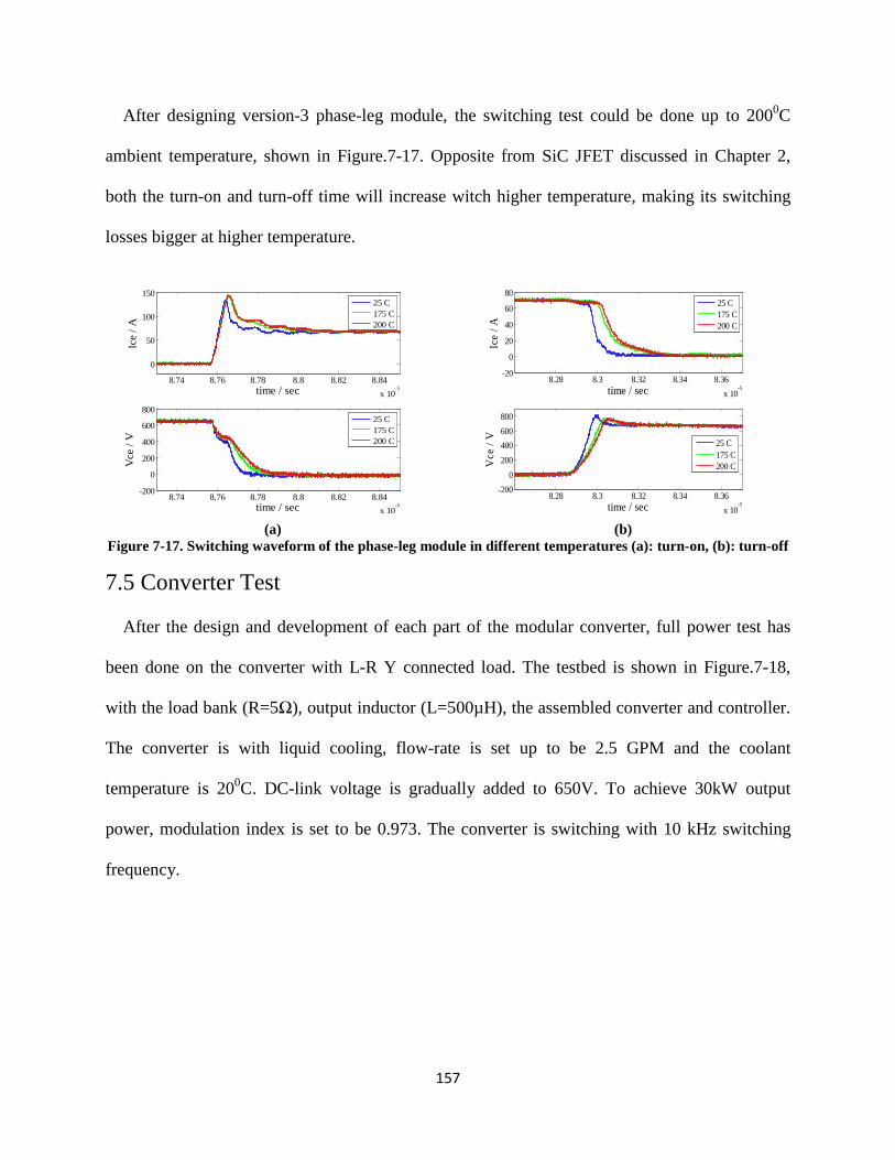
157
After designing version-3 phase-leg module, the switching test could be done up to 2000C
ambient temperature, shown in Figure.7-17. Opposite from SiC JFET discussed in Chapter 2,
both the turn-on and turn-off time will increase witch higher temperature, making its switching
losses bigger at higher temperature.
(a)
(b)
Figure 7-17. Switching waveform of the phase-leg module in different temperatures (a): turn-on, (b): turn-off
7.5 Converter Test
After the design and development of each part of the modular converter, full power test has
been done on the converter with L-R Y connected load. The testbed is shown in Figure.7-18,
with the load bank (R=5Ω), output inductor (L=500µH), the assembled converter and controller.
The converter is with liquid cooling, flow-rate is set up to be 2.5 GPM and the coolant
temperature is 200C. DC-link voltage is gradually added to 650V. To achieve 30kW output
power, modulation index is set to be 0.973. The converter is switching with 10 kHz switching
frequency.
8.74 8.76 8.78 8.8 8.82 8.84
x 10-5
0
50
100
150
time / sec
Ice / A
8.74 8.76 8.78 8.8 8.82 8.84
x 10-5
-200
0
200
400
600
800
time / sec
Vce
/ V
25 C175 C200 C
25 C175 C200 C
8.28 8.3 8.32 8.34 8.36
x 10-5
-20
0
20
40
60
80
time / sec
Ice
/ A
8.28 8.3 8.32 8.34 8.36
x 10-5
-200
0
200
400
600
800
time / sec
Vce
/ V
25 C175 C200 C
25 C175 C200 C

158
ConverterInductor ControllerLoad
Liquid cooling
Figure 7-18. Picture of the full power testbed
Experimental results with SVPWM and DPWM are shown in Figure.7-19 and Figure.7-20,
with the DC-link voltage to be 650V, the three-level line-to-line output voltage jumping from -
325V to 325V and load current with 46A RMS value. 30 kW output power is reached and 6.4
kW/kg power density is realized. As discussed in Chapter.5, DPWM generates bigger current
ripple than SVPWM.
Figure 7-19. Experimental results of the modular converter with 30kW output power with SVPWM

159
Figure 7-20. Experimental results of the modular converter with 30kW output power with DPWM
7.6 Conclusions
In this chapter, the hardware design and development based on modular design method are
introduced. With the brief introduction of the SiC JFET/SBD based AC-DC-AC converter
development, most of the chapter introduced the development of the DC-AC converter with Si
IGBT modules.
First, modular converter (motor drive) architecture is proposed in this chapter, which could be
separated for three main parts: controller, mother board and phase-leg modules. With this kind of
architecture, the converter development could be modular and realized concurrently by each part.
Then the design procedure is introduced with the proposed architecture. Controller, mother
board and phase-leg modules development are parallel. The phase-leg modules are evaluated
with switching test and redesigned to improve the performance for converter assembly.
Design example of a 30kW three-phase inverter is introduced to demonstrate the modular
design method. Floating DSP (TMS320F28335) is used for the controller, with 10kW phase-leg

160
modules assembling to the mother board. The problem of version-1 phase-leg module causes the
slowing down of gate driver and makes the switching loss bigger. With the modification of gate
driver power suppliers, version-2 phase-leg modules effectively increase the switching speed.
Then with the improved gate driver, high temperature package based version-3 phase-leg module
is developed and evaluated. The modular design method makes the development faster and more
reliable.
Full power test has been done for the version-1 phase-leg module based three-phase inverter,
showing the designed output power is realized.

161
Chapter 8. Conclusions and Future Work
On the basis of the work presented in chapter 1~7, the conclusions of this dissertation are
summarized in this chapter. The future works of the dissertation are also proposed in this chapter.
8.1 Conclusions
This dissertation presented a systematic methodology of design and control of high density
motor drive with consideration of power electronics devices, passive filter, PWM methods and
motor control strategies. Following conclusions could be drawn:
First, the application of SiC devices could increase the power density of the motor drive, not
only by reducing the passive filter with fast switching speed but also by reducing the heatsink
size by the ability of working at high temperature. This dissertation developed the methods to
evaluate the conduction and switching performance of the SiC JFET and SiC SBD in the motor
drive phase-leg and estimated the motor drive power loss at different temperatures. With SiC
SBD as the freewheeling diode, both the conduction and switching loss of the motor drive could
be reduced comparing with diode-less motor drive especially at higher temperature. Without SiC
SBD, the current overshooting in the SiC JFET at high temperature could be unacceptable. When
SiC SBD is paralleled with SiC JFET in the motor drive, the advantages of SiC devices at high
temperature could really show benefit.
Second, input filter design for the active front-end rectifier of the motor drive is studied. Based
on the classical L-C filter design method, the parasitic parameters could obviously influence the
filter performance. Physical design to improve the filter parasitic parameters could improve the
EMI noise especially in high frequency range. Random PWM method is another method to

162
improve the EMI noise of the active-front rectifier by spreading the noise energy in wider range
without impairing the power quality.
Third, the common-mode noise current reduction for the inverter of the motor drive is studied.
The converter modulation works as the noise source and the L-R-C series equivalent circuit
works as the CM noise path, which has a resonant frequency. AZSPWM and NSPWM perform
as improved PWM methods on the basis of SVPWM and DPWM and could effectively reduce
the CM voltage amplitude to 1/3, but also bring some higher harmonics. These harmonics could
be amplified in CM current when they are close to the resonant frequency. The PWM methods
and switching frequency design should be together with the CM loop impedance. Also, the CM
modulation signal could also contribute to the CM noise especially for DPWM/NSPWM at low
modulation index, which should be paid attention to.
Fourth, constant switching frequency PWM (CSFPWM) simply treats the switching frequency
to be constant and loses one important freedom. Variable switching frequency PWM (VSFPWM)
methods are designed to improve efficiency and EMI. Current ripple in the three-phase converter
is determined by the switching action of the three phase legs, and could be predicted with eight
different Thevenin equivalent circuits of the eight voltage vectors. Simulation and experiments
validate the prediction. Based on the prediction, VSFPWM architecture is proposed in this
dissertation, and with ripple current peak and RMS requirements, VSFPWM1 and VSFPWM 2
are proposed. VSFPWM1 could reduce the switching losses and improve EMI without exceeding
the ripple current peak value requirement; VSFPWM2 could improve EMI by keeping the ripple
current RMS value the same with CSFPWM. Simulation and experiments prove the feasibility
and benefits of the VSFPWM methods.

163
Fifth, the special issue of motor sensorless control with high density motor drive is studied
with experiments on an axial flux PM motor. There is an obvious transient when the motor drive
is switched from open loop control to sensorless control, and with the high density designed
small DC-link capacitor, this transient is extremely serious. There are two main reasons for the
transient: the reference angle difference and the sudden change of q-axis reference current. With
the improved starting process proposed in the dissertation, the transient can be significantly
reduced and the motor can be pushed to high power and speed with the motor drive with speed
sensorless control method.
In the end, the high density motor drive hardware implementation is realized with modular
motor drive design method. The architecture of multi-phase voltage source inverter based
modular motor drive structure is proposed in the dissertation. With the modular design method,
the controller, mother board and phase-leg modules are being developed concurrently and then
assembled and tested. The phase-leg module is evaluated by switching test and re-designed for
performance improvement. Full power (30 kW) test has been done for the modular converter.
8.2 Future work
Based on the work presented in the dissertation, several further studies for motor drive’s
density improvement could be done in the future:
(1) For device part, although SiC devices push the switching speed to a much higher level
than Si devices and have better high temperature performance, some non-ideal effects
limit the increasing of switching speed. The cross-talk phenomenon is a typical problem,
which brings interferences to the gate driver when the other device in the phase-leg is
switching. The solution in this dissertation is simply slowing the switching speed by
adding an extra gate capacitor. The physical principle of cross-talk needs to be

164
understood, and an active solution is expected to solve the problem without reducing the
switching speed.
(2) This dissertation studies the CM reduction PWM methods and VSFPWM methods
separately, for a systematical application these methods need to be combined together for
CM/DM EMI reduction. Further study could be done for applying a more general PWM
method for motor drives.
(3) PWM methods’ influence on the EMI noise mainly improves the mid-frequency range
(below 5MHz), for the higher frequency range, a passive filter is the main way to
improve. This dissertation studies how the passive filter influences the high frequency
EMI, but does not give a good solution. Further study could be done for an integrated
filter for high frequency EMI reduction.
(4) VSFPWM methods for motor drive still keep the DC-link voltage constant. Actually at
low speed, the modulation index will be low and brings some problems. If the DC-link
voltage could also be a variable value together with the motor speed, efficiency and EMI
could be further improved.
(5) The modular motor drive design has been done to build a three-phase converter with
version-1 phase-leg modules. Updated phase-leg modules could be also applied to the
multi-phase converter, and comparison of loss could be done to show the method’s
benefit.

165
References
[1] R. Lai, “Analysis and Design for a High Power Density Three-phase AC Converter Using SiC
Devices” PhD Dissertation, Virginia Polytechnic Institute and State University, Blacksburg, VA. 2008
[2] Oak Ridge National Laboratory, “High Power Density Integrated Traction Machine Drive”, Research
Proposal, 2010
[3] M. Ehsani, Y. Gao, J. M. Miller, “Hybrid Electric Vehicles: Architecture and Motor Drives,”
Proceedings of the IEEE, vol.95, no.4, pp.719-728, April 2007
[4] Z. Q. Zhu, D. Howe, “Electrical Machines and Drives for Electric, Hybrid, and Fuel Cell Vehicles,”
Proceedings of the IEEE, vol.95, no.4, pp.746-765, April 2007
[5] J. A. Weimer, “The role of electric machines and drives in the more electric aircraft,” Electric
Machines and Drives Conference, 2003. IEMDC’03. IEEE International, vol.1, no., pp. 11- 15 vol.1, 1-4
June 2003
[6] J. W. Bennett, B. C. Mecrow, A. G. Jack, D. J. Atkinson, “A Prototype Electrical Actuator for Aircraft
Flaps,” IEEE Transactions on Industrial Application, vol.46, no.3, pp.915-921, May-June 2010
[7] D. S. Parker, C. G. Hodge, “The electric warship [electric propulsion],” Power Engineering Journal,
vol.12, no.1, pp.5-13, Feb 1998
[8] J. M. Apsley, A. Gonzalez-Villasenor, M. Barnes, A. C. Smith, S. Williamson, J. D. Schuddebeurs, P.
J. Norman, C. D. Booth, G. M. Burt, J. R. McDonald, “Propulsion Drive Models for Full Electric Marine
Propulsion Systems,” IEEE Transactions on Industrial Applications, vol.45, no.2, pp.676-684, March-
April 2009
[9] Y. Khersonsky, R. Lee, C. Mak, “High efficiency quiet electric drive,” Power Electronics, Machines
and Drives, 2004. (PEMD 2004). Second International Conference on, vol.2, no., pp. 568- 573 Vol.2, 31
March-2 April 2004
[10] J. W. Kolar, U. Drofenik, J. Biela, M. L. Heldwein, H. Ertl, T. Friedli, S. D. Round, “PWM
Converter Power Density Barriers,” Power Conversion Conference - Nagoya, 2007. PCC ‘07, vol., no.,
pp.P-9-P-29, 2-5 April 2007
[11] J. S. Lai, D. J. Nelson, “Energy Management Power Converters in Hybrid Electric and Fuel Cell
Vehicles,” Proceedings of the IEEE, vol.95, no.4, pp.766-777, April 2007
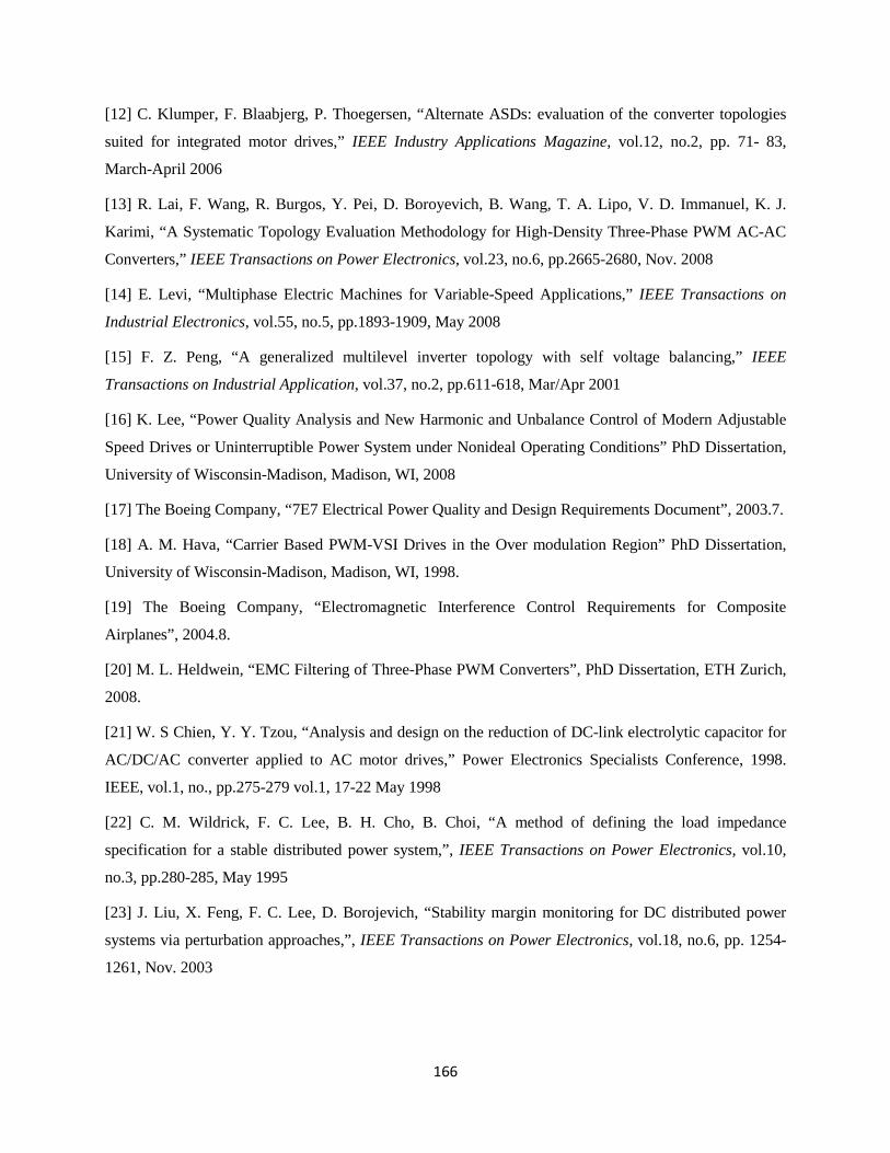
166
[12] C. Klumper, F. Blaabjerg, P. Thoegersen, “Alternate ASDs: evaluation of the converter topologies
suited for integrated motor drives,” IEEE Industry Applications Magazine, vol.12, no.2, pp. 71- 83,
March-April 2006
[13] R. Lai, F. Wang, R. Burgos, Y. Pei, D. Boroyevich, B. Wang, T. A. Lipo, V. D. Immanuel, K. J.
Karimi, “A Systematic Topology Evaluation Methodology for High-Density Three-Phase PWM AC-AC
Converters,” IEEE Transactions on Power Electronics, vol.23, no.6, pp.2665-2680, Nov. 2008
[14] E. Levi, “Multiphase Electric Machines for Variable-Speed Applications,” IEEE Transactions on
Industrial Electronics, vol.55, no.5, pp.1893-1909, May 2008
[15] F. Z. Peng, “A generalized multilevel inverter topology with self voltage balancing,” IEEE
Transactions on Industrial Application, vol.37, no.2, pp.611-618, Mar/Apr 2001
[16] K. Lee, “Power Quality Analysis and New Harmonic and Unbalance Control of Modern Adjustable
Speed Drives or Uninterruptible Power System under Nonideal Operating Conditions” PhD Dissertation,
University of Wisconsin-Madison, Madison, WI, 2008
[17] The Boeing Company, “7E7 Electrical Power Quality and Design Requirements Document”, 2003.7.
[18] A. M. Hava, “Carrier Based PWM-VSI Drives in the Over modulation Region” PhD Dissertation,
University of Wisconsin-Madison, Madison, WI, 1998.
[19] The Boeing Company, “Electromagnetic Interference Control Requirements for Composite
Airplanes”, 2004.8.
[20] M. L. Heldwein, “EMC Filtering of Three-Phase PWM Converters”, PhD Dissertation, ETH Zurich,
2008.
[21] W. S Chien, Y. Y. Tzou, “Analysis and design on the reduction of DC-link electrolytic capacitor for
AC/DC/AC converter applied to AC motor drives,” Power Electronics Specialists Conference, 1998.
IEEE, vol.1, no., pp.275-279 vol.1, 17-22 May 1998
[22] C. M. Wildrick, F. C. Lee, B. H. Cho, B. Choi, “A method of defining the load impedance
specification for a stable distributed power system,”, IEEE Transactions on Power Electronics, vol.10,
no.3, pp.280-285, May 1995
[23] J. Liu, X. Feng, F. C. Lee, D. Borojevich, “Stability margin monitoring for DC distributed power
systems via perturbation approaches,”, IEEE Transactions on Power Electronics, vol.18, no.6, pp. 1254-
1261, Nov. 2003

167
[24] R. Burgos, Z. Chen, D. Boroyevich, F. Wang, “Design considerations of a fast 0-Ω gate-drive circuit
for 1.2 kV SiC JFET devices in phase-leg configuration,” Energy Conversion Congress and Exposition,
2009. ECCE. IEEE , vol., no., pp.2293-2300, 20-24 Sept. 2009
[25] T. Funaki, J. C. Balda, J. Junghans, A. S. Kashyap, H. A. Mantooth, F.Barlow, T. Kimoto, T.
Hikihara, “Power Conversion With SiC Devices at Extremely High Ambient Temperatures”, IEEE
Transactions on Power Electronics, vol.22, no.4, pp.1321-1329, July 2007
[26] R. Lai, F. Wang, P. Ning, D. Zhang, D. Jiang, R. Burgos, D. Boroyevich, K. J. Karimi, V. D.
Immanuel, “Development of a 10 kW high power density three-phase ac-dc-ac converter using SiC
devices,” Power Electronics and Applications, 2009. EPE '09. 13th European Conference on , vol., no.,
pp.1-12, 8-10 Sept. 2009
[27] P. Ning, R. Lai, D. Huff, F. Wang, K. D. T. Ngo, V. D. Immanuel, K. J. Karimi, “SiC Wirebond
Multichip Phase-Leg Module Packaging Design and Testing for Harsh Environment,” Power Electronics,
IEEE Transactions on Power Electronics, vol.25, no.1, pp.16-23, Jan. 2010
[28] T. Friedli, S. D. Round, D. Hassler, J. W. Kolar, “Design and Performance of a 200-kHz All-SiC
JFET Current DC-Link Back-to-Back Converter,”, IEEE Transactions on Industry Applications, vol.45,
no.5, pp.1868-1878, Sept.-oct. 2009
[29] E. Cilio, J. Homberger, B. McPherson, R. Schupbach, A. Lostetter, J. Garrett, “A Novel High
Density 100kW Three-Phase Silicon Carbide (SiC) Multichip Power Module (MCPM) Inverter,” Applied
Power Electronics Conference, APEC 2007 - Twenty Second Annual IEEE , vol., no., pp.666-672, Feb.
25 2007-March 1 2007
[30] B. Ozpineci, M. S. Chinthavali, L. M. Tolbert, A. S. Kashyap, H. A. Mantooth, “A 55-kW Three-
Phase Inverter With Si IGBTs and SiC Schottky Diodes,”, IEEE Transactions on Industry Applications,
vol.45, no.1, pp.278-285, Jan.-Feb. 2009
[31] P. Sun, J. S. Lai, H. Qian, W. Yu, C. Smith, J. Bates, B. Arnet, A. Litvinov, S. Leslie, “Efficiency
evaluation of a 55kW soft-switching module based inverter for high temperature hybrid electric vehicle
drives application,” Applied Power Electronics Conference and Exposition (APEC), 2010 Twenty-Fifth
Annual IEEE , vol., no., pp.474-479, 21-25 Feb. 2010
[32] Y. Li, F. C. Lee, D. Boroyevich, “A three-phase soft-transition inverter with a novel control strategy
for zero-current and near zero-voltage switching,” IEEE Transactions on Power Electronics, vol.16, no.5,
pp.710-723, Sep 2001
[33] M. L. Heldwein, J. W. Kolar, “Impact of EMC Filters on the Power Density of Modern Three-Phase
PWM Converters,” IEEE Transactions on Power Electronics, vol.24, no.6, pp.1577-1588, June 2009

168
[34] H. Akagi, T. Shimizu, “Attenuation of Conducted EMI Emissions From an Inverter-Driven Motor,”
IEEE Transactions on Power Electronics, vol.23, no.1, pp.282-290, Jan. 2008
[35] S. Wang, F. C. Lee, W. G. Odendaal, J. D. van Wyk, “Improvement of EMI filter performance with
parasitic coupling cancellation,” IEEE Transactions on Power Electronics, vol.20, no.5, pp. 1221-1228,
Sept. 2005
[36] M. L. Heldwein, J. W. Kolar, “Winding Capacitance Cancellation for Three-Phase EMC Input
Filters,” IEEE Transactions on Power Electronics, vol.23, no.4, pp.2062-2074, July 2008
[37] K. Kretschmar, H. P. Nee, “An AC converter with a small DC link capacitor for a 15 kW permanent
magnet synchronous integral motor,” Power Electronics and Variable Speed Drives, 1998. Seventh
International Conference on, vol., no., pp.622-625, 21-23 Sep 1998
[38] E. P. Wiechmann, P. Aqueveque, R. Burgos, J. Rodriguez, “On the Efficiency of Voltage Source and
Current Source Inverters for High-Power Drives,” IEEE Transactions on Industrial Electronics, vol.55,
no.4, pp.1771-1782, April 2008
[39] K. Zhou, D. Wang, “Relationship between space-vector modulation and three-phase carrier-based
PWM: a comprehensive analysis [three-phase inverters],” IEEE Transactions on Industrial Electronics,
vol.49, no.1, pp.186-196, Feb 2002
[40] D. W. Chung, S. K. Sul, “Minimum-loss strategy for three-phase PWM rectifier,” IEEE Transactions
on Industrial Electronics, vol.46, no.3, pp.517-526, Jun 1999
[41] F. Blaabjerg, U. Jaeger, S. Munk-Nielsen, “Power losses in PWM-VSI inverter using NPT or PT
IGBT devices,” IEEE Transactions on Power Electronics, vol.10, no.3, pp.358-367, May 1995
[42] G. Narayanan, V. T. Ranganathan, D. Zhao, H. K. Krishnamurthy, R. Ayyanar, “Space Vector Based
Hybrid PWM Techniques for Reduced Current Ripple,” IEEE Transactions on Industrial Electronics,
vol.55, no.4, pp.1614-1627, April 2008
[43] A. R. Beig, G. Narayanan, V. T. Ranganathan, “Modified SVPWM Algorithm for Three Level VSI
With Synchronized and Symmetrical Waveforms,”, IEEE Transactions on Industrial Electronics, vol.54,
no.1, pp.486-494, Feb. 2007
[44] X. Mao, R. Ayyanar, H. K. Krishnamurthy, “Optimal Variable Switching Frequency Scheme for
Reducing Switching Loss in Single-Phase Inverters Based on Time-Domain Ripple Analysis,” IEEE
Transactions on Power Electronics, vol.24, no.4, pp.991-1001, April 2009

169
[45] A. M. Trzynadlowski, F. Blaabjerg, J. K. Pedersen, R. L. Kirlin, S. Legowski, “Random pulse width
modulation techniques for converter-fed drive systems-a review,” IEEE Transactions on Industry
Applications, vol.30, no.5, pp.1166-1175, Sep/Oct 1994
[46] C. B. Jacobina, A. M. N. Lima, E. R. C. da Silva, A. M. Trzynadlowski, “Current control for
induction motor drives using random PWM,” IEEE Transactions on Industrial Electronics, vol.45, no.5,
pp.704-712, Oct 1998
[47] A. M. Trzynadlowski, K. Borisov, K, Y. Li, L. Qin, “A novel random PWM technique with low
computational overhead and constant sampling frequency for high-volume, low-cost applications,” IEEE
Transactions on Power Electronics, vol.20, no.1, pp. 116-122, Jan. 2005
[48] B. K. Bose “Modern Power Electronics and AC Drives”. China Machine Press, 2002
[49] R. Krishnan “Permanent Magnet Synchronous and Brushless DC Motor Drives”, CRC Press, 2009
[50] J. Holtz, “Sensorless Control of Induction Machines—With or Without Signal Injection?,” IEEE
Transactions on Industrial Electronics, vol.53, no.1, pp. 7- 30, Feb. 2006
[51] R. Burgos, P. Kshirsagar, A. Lidozzi, F. Wang, D. Boroyevich, “Mathematical Model and Control
Design for Sensorless Vector Control of Permanent Magnet Synchronous Machines”, Computers in
Power Electronics, 2006. COMPEL '06. IEEE Workshops on
[52] P. Kshirsagar, R. Burgos, A. Lidozzi, J. Jang, F. Wang, D. Boroyevich, S. K. Sul, “Implementation
and Sensorless Vector-Control Design and Tuning Strategy for SMPM Machines in Fan-Type
Applications,” Industry Applications Conference, 2006. 41st IAS Annual Meeting
[53] A. I. Maswood, F. Liu, “A novel unity power factor input stage for AC drive application,” IEEE
Transactions on Power Electronics, vol.20, no.4, pp. 839- 846, July 2005
[54] M. A. Huque, L. M. Tolbert, B. J. Blalock, S. K. Islam, “Silicon-on-insulator-based high-voltage,
high-temperature integrated circuit gate driver for silicon carbide-based power field effect transistors,”
IET Power Electronics, vol.3, no.6, pp.1001-1009, Nov. 2010
[55] M. Pasko, M. Maciazek, D. Bula, “Performance and accuracy comparison of fixed and floating-point
realizations of the Active Power Filter control algorithm,” Nonsinusoidal Currents and Compensation,
2008. ISNCC 2008. International School on , vol., no., pp.1-4, 10-13 June 2008
[56] Texas Instrument “Next-Generation Embedded Motor Control from Texas Instruments” 2004
[57] D. Bergogne, H. Morel, D. Planson, D. Tournier, P. Bevilacqua, B. Allard, R. Meuret, S. Vieillard, S.
Rael, F. MeibodyTabar, “Towards an airborne high temperature SiC inverter,” Power Electronics
Specialists Conference, 2008. PESC 2008. IEEE, vol., no., pp.3178-3183, 15-19 June 2008

170
[58] T. Zhao, J. Wang, A. Q. Huang, A. Agarwal, “Comparisons of SiC MOSFET and Si IGBT Based
Motor Drive Systems,” Industry Applications Conference, 2007. 42nd IAS Annual Meeting. Conference
Record of the 2007 IEEE, vol., no., pp.331-335, 23-27 Sept. 2007
[59] H. Chang, E. Hanna, A. V. Radun, “Development and demonstration of silicon carbide (SiC) motor
drive inverter modules,” Power Electronics Specialist Conference, 2003. PESC '03. 2003 IEEE 34th
Annual, vol.1, no., pp. 211-216 vol.1, 15-19 June 2003
[60] C. Cass, Y. Wang, R. Burgos, T. P. Chow, F. Wang, D. Boroyevich, “Evaluation of SiC JFETs for a
Three-Phase Current-Source Rectifier with High Switching Frequency,” Applied Power Electronics
Conference, APEC 2007 - Twenty Second Annual IEEE , vol., no., pp.345-351, Feb. 25 2007-March 1
2007
[61] T. Funaki, A. S. Kashyap, H. A. Mantooth, J. C. Balda, F. D. Barlow, T. Kimoto, T. Hikihara,
“Characterization of SiC diodes in extremely high temperature ambient,” Applied Power Electronics
Conference and Exposition, 2006. APEC '06. Twenty-First Annual IEEE , vol., no., pp. 7 pp.-, 19-23
March 2006
[62] R. Singh, J. A. Cooper, M. R. Melloch, T. P. Chow, J. W. Palmour, “SiC power Schottky and PiN
diodes,” IEEE Transactions on Electron Devices, vol.49, no.4, pp.665-672, Apr 2002
[63] A. Elasser, M. H. Kheraluwala, M. Ghezzo, R. L. Steigerwald, N. A. Evers, J. Kretchmer, T. P.
Chow, “A comparative evaluation of new silicon carbide diodes and state-of-the-art silicon diodes for
power electronic applications,”, IEEE Transactions on Industry Applications, vol.39, no.4, pp. 915-921,
July-Aug. 2003
[64] S. Round, M. Heldwein, J. W. Kolar, I. Hofsajer, P. Friedrichs, “A SiC JFET driver for a 5 kW, 150
kHz three-phase PWM converter,” Industry Applications Conference, 2005. Fourtieth IAS Annual
Meeting. Conference Record of the 2005 , vol.1, no., pp. 410-416 Vol. 1, 2-6 Oct. 2005
[65] R. Lai, F. Wang, R. Burgos, D. Boroyevich, “Voltage balance control of non-regenerative three-level
boost rectifier using carrier-based pulse width modulation,” Power Electronics Specialists Conference,
2008. PESC 2008. IEEE , vol., no., pp.3137-3142, 15-19 June 2008
[66] S. Wang, F. C. Lee, J. D. van Wyk, “A Study of Integration of Parasitic Cancellation Techniques for
EMI Filter Design With Discrete Components,” IEEE Transactions on Power Electronics, vol.23, no.6,
pp.3094-3102, Nov. 2008
[67] T. G. Habetler, D. M. Divan, “Acoustic noise reduction in sinusoidal PWM drives using a randomly
modulated carrier,” IEEE Transactions on Power Electronics, vol.6, no.3, pp.356-363, Jul 1991

171
[68] A. M. Trzynadlowski, M. M. Bech, F. Blaabjerg, J. K. Pedersen, R. L. Kirlin, M. Zigliotto,
“Optimization of switching frequencies in the limited-pool random space vector PWM strategy for
inverter-fed drives,” IEEE Transactions on Power Electronics, vol.16, no.6, pp.852-857, Nov 2001
[69] K. Borisov, T. E. Calvert, J. A. Kleppe, E. Martin, A. M. Trzynadlowski, “Experimental
investigation of a naval propulsion drive model with the PWM-based attenuation of the acoustic and
electromagnetic noise,” Industrial Electronics, IEEE Transactions on , vol.53, no.2, pp. 450-457, April
2006
[70] M. J. Nave, “On modeling the common mode inductor,” Electromagnetic Compatibility, 1991.
Symposium Record., IEEE 1991 International Symposium on , vol., no., pp.452-457, 12-16 Aug 1991
[71] S. Kaboli, A. H. Rajaei, A. Sheikhi, “Application of random PWM techniques for reducing the
electromagnetic interference of Vienna rectifiers in distribution power system,” Power Electronics and
Motion Control Conference, 2009. IPEMC '09. IEEE 6th International , vol., no., pp.998-1003, 17-20
May 2009
[72] S. Kaboli, J. Mahdavi, A. Agah, “Application of Random PWM Technique for Reducing the
Conducted Electromagnetic Emissions in Active Filters,” IEEE Transactions on Industrial Electronics,
vol.54, no.4, pp.2333-2343, Aug. 2007
[73] J. F. Gieras, R. Wang, M. J. Kamper, “Axial Flux Permanent Magnet Brushless Machines,” Kluwer
Academic Publishers, 2004
[74] R.Lai, F. Wang, R. Burgos, D. Boroyevich, “Voltage balance control of non-regenerative three-level
boost rectifier using carrier-based pulse width modulation,” Power Electronics Specialists Conference,
2008. PESC 2008. IEEE , vol., no., pp.3137-3142, 15-19 June 2008
[75] H. Akagi, T. Shimizu, “Attenuation of Conducted EMI Emissions From an Inverter-Driven Motor,”,
IEEE Transactions on Power Electronics, vol.23, no.1, pp.282-290, Jan. 2008
[76] E. Un, A. M. Hava, “A Near-State PWM Method With Reduced Switching Losses and Reduced
Common-Mode Voltage for Three-Phase Voltage Source Inverters,” IEEE Transactions on Industry
Applications, vol.45, no.2, pp.782-793, March-April 2009
[77] A. M. Hava, N. O. Cetin, E. Un, “On the Contribution of PWM Methods to the Common Mode
(Leakage) Current in Conventional Three-Phase Two-Level Inverters as Applied to AC Motor Drives,”
Industry Applications Society Annual Meeting, 2008. IAS '08. IEEE , vol., no., pp.1-8, 5-9 Oct. 2008
172
[78] N. O. Cetin, A. M. Hava, “Interaction between the filter and PWM units in the sine filter
configuration utilizing three-phase AC motor drives employing PWM inverters,” Energy Conversion
Congress and Exposition (ECCE), 2010 IEEE , vol., no., pp.2592-2599, 12-16 Sept. 2010
[79] F. Luo, S. Wang, F. Wang, D. Boroyevich, N. Gazel, Y. Kang. A. C. Baisden, “Analysis of CM
Volt-Second Influence on CM Inductor Saturation and Design for Input EMI Filters in Three-Phase DC-
Fed Motor Drive Systems,” IEEE Transactions on Power Electronics, vol.25, no.7, pp.1905-1914, July
2010
[80] A. Muetze, “Scaling Issues for Common-Mode Chokes to Mitigate Ground Currents in Inverter-
Based Drive Systems,”, IEEE Transactions on Industry Applications, vol.45, no.1, pp.286-294, Jan.-Feb.
2009
[81] W. Shen, F. Wang, D. Boroyevich, C. W. Tipton, “Loss Characterization and Calculation of
Nanocrystalline Cores for High-Frequency Magnetics Applications,” IEEE Transactions on Power
Electronics, vol.23, no.1, pp.475-484, Jan. 2008
[82] D. Zhang, F. Wang, R. Burgos, R. Lai, D. Boroyevich, D, “Impact of Interleaving on AC Passive
Components of Paralleled Three-Phase Voltage-Source Converters,” IEEE Transactions on Industry
Applications, vol.46, no.3, pp.1042-1054, May-June 2010
[83] D. Zhang, F. Wang, R. Burgos, D. Boroyevich, “Common mode circulating current control of
interleaved three-phase two-level voltage-source converters with discontinuous space-vector modulation,”
Energy Conversion Congress and Exposition, 2009. ECCE 2009. IEEE , vol., no., pp.2801-2807, 20-24
Sept. 2009
[84] S. K. T. Miller, T. Beechner, J. Sun, “A Comprehensive Study of Harmonic Cancellation Effects in
Interleaved Three-Phase VSCs,” Power Electronics Specialists Conference, 2007. PESC 2007. IEEE , vol.,
no., pp.29-35, 17-21 June 2007
[85] J. W. Kimball, M. Zawodniok, “Reducing common-mode voltage in three-phase sine-triangle PWM
with interleaved carriers,” Applied Power Electronics Conference and Exposition (APEC), 2010 Twenty-
Fifth Annual IEEE , vol., no., pp.1508-1513, 21-25 Feb. 2010
[86] G. Francis, R. Burgos, P. Rodriguez, F. Wang, D. Boroyevich, R. Liu, A. Monti, “Virtual
Prototyping of Universal Control Architecture Systems by means of Processor in the Loop Technology,”
Applied Power Electronics Conference, APEC 2007 - Twenty Second Annual IEEE , vol., no., pp.21-27,
Feb. 25 2007-March 1 2007
[87] W.Ouyang, “Modular Permanent Magnet Machine Drive System With Fault Tolerant Capability”
PhD Dissertation, University of Wisconsin-Madison, Madison, WI, 2008

173
[88] L. Wei, et. “ Pulse Width Modulation (PWM) Rectifier with Variable Switching Frequency”, US
patent 7190143132, Mar. 2007
[89] D. Zhang, F. Wang, S. El-Barbari, J. Sabate, D.Boroyevich, “Improved asymmetric space vector
modulation for voltage source converters with low carrier ratio,” Applied Power Electronics Conference
and Exposition (APEC), 2010 Twenty-Fifth Annual IEEE , vol., no., pp.1487-1493, 21-25 Feb. 2010
[90] D. Dujic, M. Jones, E. Levi, J. Prieto, F. Barrero, “Switching Ripple Characteristics of Space Vector
PWM Schemes for Five-Phase Two-Level Voltage Source Inverters—Part 1: Flux Harmonic Distortion
Factors,” IEEE Transactions on Industrial Electronics, vol.58, no.7, pp.2789-2798, July 2011
[91] M. Jones, D. Dujic, E. Levi, J. Prieto, F. Barrero, “Switching Ripple Characteristics of Space Vector
PWM Schemes for Five-Phase Two-Level Voltage Source Inverters—Part 2: Current Ripple,” IEEE
Transactions on Industrial Electronics , vol.58, no.7, pp.2799-2808, July 2011

174
VITA
Dong Jiang was born in Changsha, Hunan Province in P.R.China on April 5th, 1983. He
received his B.S and M.S degree in Electrical Engineering from Tsinghua University, Beijing,
China, in 2005 and 2007 respectively. He began his PhD study in Virginia Polytechnic Institute
and State University in 2007. In 2010, he was transferred to the University of Tennessee to
continue his PhD study.