Embed Size (px)
Citation preview
MLRITM Department of ECE
IC APPLICATIONS AND HDL SIMULATION LAB
1
Department of Electronics & Communication Engineering
III Year B.Tech. ECE - I Sem L T/P/D C
0 /3/- 2
IC APPLICATIONS AND HDL SIMULATION LAB
Note: Minimum of 16 experiments have to be conducted ( at least Seven from each part):
Part-I
Linear IC Experiments
1. Op-amp Applications-Adder, Subtractor, Comparator
2. Integrator and Differentiator using IC741 Op-Amp.
3. Active Filter Applications-LPF,HPF(First Order)
4. IC 741 waveform Generators- Sine, Square wave and Triangular waves
5. IC 555 Mono Stable and Astable Multivibrator Circuits
6. Schmitt Trigger Circuits-using IC741
7. IC 565 – PLL applications
8. Voltage regulator IC 723, three terminal voltage regulators- 7805, 7809, 7912.
Part-II
HDL Simulation Programmes
1. HDL Code to Realize the all logic gates
2. Design of 2 to 4 Decoder
3. Design of 8-to-3 encoder(without and with priority)
4. Design of 8-to-1 multiplexer and 1-to-8 demultiplexer
5. Design of 4 bit binary to gray code converter
6. Design of 4 bit comparator
7. Design of Full adder using 3 modeling Styles
8. Design of Flip-Flops: SR,D,JK,T
9. Design of 4-bit binary, BCD Counters (Synchronous/Asynchronous reset)
10. Finite State Machine Design

MLRITM Department of ECE
IC APPLICATIONS AND HDL SIMULATION LAB
2
Part-I
INTRODUCTION TO IC APPLICATIONS LAB
The operational amplifier forms the basic building block for most of the linear
IC’s. It is a direct coupled high gain amplifier usually consisting of one or more
differential amplifiers and followed by a level translator and an output stage. A few
applications of an Op-amp are, instrumentation, voltage to current or current to voltage
converter, integrator, Differentiator, oscillators, Filters, clippers and Clampers, sample and
hold, analog to digital converter, adder, sub tractor, scale changer, comparator etc.,
Now-a-days, the op-amp has become a basic analog building block common to a
number of electronic functions performed in instrumentation, computation and control.
Op-amp is basically a differential amplifier whose basic function is to amplify the
difference between two input signals. Therefore it is also called as "difference amplifier".
The bias levels and the gain characteristic of a differential stage depend on the symmetry,
between two branches of the circuit. The balanced nature of the differential amplifiers
makes it ideal as a gain block for monolithic op-amp, since the close matching and the
temperature tracking properties of monolithic components are far better than their discrete
counter parts.
The ideal operational amplifier is shown in fig. below
A signal appearing at the negative terminal (VI) is inverted at the output, a signal at the
positive terminal (V 2) appears at the output with no change in sign. Hence the negative
terminal is called the "inverting" the positive terminal the "non-inverting" terminal, In
general, the output voltage is directly proportional to Vd = (Vl-V2). The constant of
proportionality -A, is the voltage gain of the amplifier.
The operational amplifier is a direct-coupled high gain amplifier to which feedback

MLRITM Department of ECE
IC APPLICATIONS AND HDL SIMULATION LAB
3
is added to control its overall response characteristics. It is often referred to as the basic
linear integrated circuit.
The ideal OP-amp has the following characteristics:
Properties Ideal Typical
Open loop gain ∞ Very high ( ≥104)
Open loop bandwidth ∞
Very high
Common-mode ∞ High (> 70dB)
rejection ratio
Input resistance ∞ High (≥10MΩ)
Output resistance 0 Low (< 500 Ω)
Off-set voltage and
current 0 Low(<10mV,<0.2nA)
General Description:
The LM 741series is general purpose operational amplifiers which feature improved
performance over industry standards like the LM 709. They are direct, plug-in
replacements for the 709C, LM 201, MC 1439 and 748 in most app1ications.
The amplifiers offer many features which make their application nearly fool proof:
Overload protection on the input and output, no latch-up when the common mode range is
exceeded, as well as freedom from oscillations.

MLRITM Department of ECE
IC APPLICATIONS AND HDL SIMULATION LAB
4
EXPERIMENT-1
OP-AMP Applications-ADDER, SUBTRACTOR&COMPARATOR
Aim: To study the applications of operational amplifier.
Equipment required:
1. Bread Board - 1no.
2. Function Generator (0-30V dual) - 1no.
3. Digital multimeter - 1no.
4. CRO(20 MHz) - 1no.
5. IC 741 - 1no.
6. Connecting wires.
Circuit Diagram:
1.Summing Amplifier

MLRITM Department of ECE
IC APPLICATIONS AND HDL SIMULATION LAB
5
Fig 1b) Non Inverting Configuration
2. Subtractor

MLRITM Department of ECE
IC APPLICATIONS AND HDL SIMULATION LAB
6
3. Basic Comparator
THEORY:
1. Summing amplifiers
Fig. shows a summing amplifier or adder circuit. Here, the output is a linear summation of
a number of input signals. Here, the feedback force virtual ground to exist at the inverting

MLRITM Department of ECE
IC APPLICATIONS AND HDL SIMULATION LAB
7
input to the ideal amplifier. Furthermore the input current to the ideal amplifier is zero.
Hence, the current i is given as
VI V2 Vn
i= + + ------
R1 R2 Rn
and Vo = -Rf i.
Thus the output voltage is equal to the negative weighted Sum of the input
voltages. The summing operation depends exclusively on the sum of the resistance ratios.
The circuit is also known as Scaling or weighted amplifier.
If R1 =R2 = --------------- =Rn then
V 0 = - Rf (Vl +V2+ --------- +Vn)
R1
and the output is proportional to the sum of the inputs.
The circuit is widely used to form linear combinations of various signals. in analog
computers. The virtual ground at the summing node prevents any interaction between the
various signal sources connected to the input terminals. The output impedance of the
summing amplifier is zero. The input impedance is different for each input signal. Because
of the virtual ground at the summing node, the input impedance seem by each signal
source is simply the resistance connecting that source to the summing node.
2. Subtractor
A basic differential amplifier can be used as a subtractor as shown in figure 2. In
this figure, input signals can be scaled to the desired values by selecting appropriate values
for the external resistors; when this is done, the circuit is referred to as scaling amplifier.
However, in figure 3 all external resistors are equal in value, so the gain of the amplifier is
equal to 1. From the figure, the output voltage of the differential amplifier with a gain of 1
is

MLRITM Department of ECE
IC APPLICATIONS AND HDL SIMULATION LAB
8
When resistors, R1 = R2 and R3 = R4 the above transfer function for the differential
amplifier can be simplified to the following expression:
Differential Amplifier Equation
Thus the output voltage V0 is equal to the voltage applied to the non inverting terminal (Vb
) minus the voltage applied to the inverting terminal(Va);hence the circuit is called a
subtractor.
3. Basic comparator:
Figure (3) shows an op-amp used as a comparator. A fixed reference voltage Vref
of 1V is applied to the (-) input, and the other time-varying signal voltage Vin is applied to
the (+) input. Because of this arrangement, the circuit is called the non inverting
comparator. When Vin is less than Vref, the output voltage V0 is at –Vsat(-VEE) because the
voltage at the (-) input is higher than that at the (+) input. On the other hand, when Vin is
greater than Vref, the (+) input becomes positive with respect to the (-) input, and V0 goes
to +Vsat (+Vcc). Thus V0 changes from one saturation level to another whenever Vin < or>
MLRITM Department of ECE
IC APPLICATIONS AND HDL SIMULATION LAB
9
Vref, as shown in figure 3(b). In short, the comparator is a type of analog-to-digital
converter. At any given time the V0 waveform shows whether Vin is greater or less than
Vref. The comparator is sometimes also called a voltage-level detector because, for a
desired value of the voltage level of Vin can be detected.
PROCEDURE:
Part 1: ADDER:
1. Connect the circuit as shown in figure(1).
2. Apply different DC input voltages at Va,Vb, and Vc and measure the output voltage Vo
using a multi meter It should be Vo = Va + Vb + Vc.
Part 2: SUBTRACTOR:
1. Connect the circuit as shown in figure(2).
2. Apply different DC input voltages at Va, andVb and measure the output voltage Vo using
a multi meter. It should be Vo = Vb – Va.
Part 3: COMPARATOR:
1. Connect the circuit as shown in figure(3a).
2. Apply a reference voltage of (say 1V), to inverting terminal of op-amp.
3. Apply a sinusoidal wave with a peak voltage more than Vref to OP-AMPs Non-
inverting terminal.
4. Observe the output at pin number 6, which will be a square wave with peak to peak
voltage of (Vsat to –Vsat).
5. Observe that when Vref is less than Vin, then the output goes to +Vsat,
When Vref is greater than Vin then output goes to –Vsat.
6. Now set another reference voltage and repeat the steps 4 and 5.
7. Draw the observed waveforms on graph sheet and obtain the practical reference voltage.
PRECAUTIONS:
i. Check the circuit connections before switching on the power supply.
ii. Check the continuity of the connecting wires.
INFERENCE:
i. The working of summing amplifier is observed & the output is calculated theoritically
and practically.

MLRITM Department of ECE
IC APPLICATIONS AND HDL SIMULATION LAB
10
ii. The working of subtractor is verified and the output is obtained, the output is calculated
theoritically and practically.
iii. The working of comparator is observed and the output is plotted, the time period &
Frequency of the output wave form is calculated.
Applications:
1.Summing amplifiers are used in amplifiers are used in an audio mixer to add different
signals with equal gains.
2. Differential amplifiers are used in Instrumentation amplifiers.
3. Comparators used in
i. Zero crossing detector
ii. Window detector
iii. Time marker generator
iv. Phase meter.
Result:
Hence the operation of Adder, Subtractor, and comparator (using 741 op amp) is verified.
Review Questions:
1. What is an operational Amplifier?
2. Characteristics of ideal op-amp?
3. Define CMRR?
4. Why op-amp s called as 741 ?
5. Name three important specifications of IC op-amp?
6. Define slew rate of op-amp
7. What is the input offset voltage of 741c op-amp
8. Define power supply sensitivity.
9. Which pins of 741 IC are called null set pins.
10. What is the bandwidth of practical op-amp.

MLRITM Department of ECE
IC APPLICATIONS AND HDL SIMULATION LAB
11
Exercise Problems:
1. Design an adder circuit using 741 op-amp to add 2V and 4V signal.
2. Design 3 input adder circuit using 741 op-amp to add 3V and 4V and 1V
signal.
3. Design a subtractor circuit using 741 op-amp to subtract 4V and 2V signal.
4. Design a comparator circuit to generate square wave output with reference
voltage 2V DC.
5. Generate a square wave by using zero cross detector.
6. Design a false triggering circuit with v ref=2V and input 5v sinusoidal signal
7. Design an adder circuit using 741 op-amp to add 2v and 4v signal .
8. Design 3 input adder circuit using 741 op-amp to add 1v and 2v and 3v signal.
9. Design a comparator circuit to generate square wave output with reference
voltage 4v DC
10. Design a subtractor circuit using 741 op-amp to subtract 3v and 1v signal.
11. Design a adder circuit to add V0=Va+Vb+Vc.
12. Design a subtractor circuit to give V0=Va-Vb
13. Generate a square wave by using zero cross detector and what are the
applications of comparator
14. Design an amplifier with a gain of +5V using one op-amp
15. Design a adder circuit to add V0=Va+Vb+Vc+Vd

MLRITM Department of ECE
IC APPLICATIONS AND HDL SIMULATION LAB
12
EXPERIMENT-2
INTEGRATOR AND DIFFERENTIATOR USING IC 741
AIM: Design and verify the functionality of Differentiator and Integrator using IC 741
Op-Amp.
EQUIPMENT REQUIRED:
1. Operational Amplifier uA 741 IC – 2No.
2. Resistors
1KΩ 1No.
1.5 KΩ 1No.
10 KΩ 1No.
15 KΩ 1No.
3. DC Power supply ( 0-30V) - 1No.
4. Bread board - 1No.
5. CRO (20MHz/30MHz) - 1No.
6. Capacitor(0.1μF) -1No.
CIRCUIT DIAGRAM:
Fig 1: Integrator
Fig 2: Differentiator

MLRITM Department of ECE
IC APPLICATIONS AND HDL SIMULATION LAB
13
THEORY:
A) INTEGRATOR:
A circuit in which “the output voltage waveform is the integral of the input voltage
waveform” is the integrator or the integration amplifier. Such a circuit is obtained by using
a basic inverting amplifier configuration, if the feedback resistor RF is replaced by a
capacitor CF.
Analysis of Integrator Circuit:
We know from first principals that the voltage on the plates of a capacitor is equal to the
charge on the capacitor divided by its capacitance giving Q/C. Then the voltage across the
capacitor is output Vout therefore: -Vout = Q/C. If the capacitor is charging and
discharging, the rate of charge of voltage across the capacitor is given as:
But dQ/dt is electric current and since the node voltage of the integrating op-amp at its
inverting input terminal is zero, X = 0, the input current I(in) flowing through the input
resistor, Rin is given as:
MLRITM Department of ECE
IC APPLICATIONS AND HDL SIMULATION LAB
14
The current flowing through the feedback capacitor C is given as:
Assuming that the input impedance of the op-amp is infinite (ideal op-amp), no current
flows into the op-amp terminal. Therefore, the nodal equation at the inverting input
terminal is given as:
From which we derive an ideal voltage output for the Op-amp Integrator as:
To simplify the math’s a little, this can also be re-written as:
Where ω = 2πƒ and the output voltage Vout is a constant 1/RC times the integral of the
input voltage Vin with respect to time. The minus sign ( – ) indicates a 180o phase shift
because the input signal is connected directly to the inverting input terminal of the op-
amp.
B) Differentiator:
The input signal to the differentiator is applied to the capacitor. The capacitor blocks any
DC content so there is no current flow to the amplifier summing point, X resulting in zero
output voltage. The capacitor only allows AC type input voltage changes to pass through
and whose frequency is dependant on the rate of change of the input signal.
At low frequencies the reactance of the capacitor is “High” resulting in a low gain
( Rƒ/Xc ) and low output voltage from the op-amp. At higher frequencies the reactance of
MLRITM Department of ECE
IC APPLICATIONS AND HDL SIMULATION LAB
15
the capacitor is much lower resulting in a higher gain and higher output voltage from the
differentiator amplifier.
However, at high frequencies an op-amp differentiator circuit becomes unstable and will
start to oscillate. This is due mainly to the first-order effect, which determines the
frequency response of the op-amp circuit causing a second-order response which, at high
frequencies gives an output voltage far higher than what would be expected. To avoid this
the high frequency gain of the circuit needs to be reduced by adding an additional small
value capacitor across the feedback resistor Rƒ.
Ok, some math’s to explain what’s going on!. Since the node voltage of the operational
amplifier at its inverting input terminal is zero, the current, i flowing through the capacitor
will be given as:
The charge on the capacitor equals Capacitance x Voltage across the capacitor
The rate of change of this charge is:
but dQ/dt is the capacitor current,i
from which we have an ideal voltage output for the op-amp differentiator is given as:
Therefore, the output voltage Vout is a constant -Rƒ.C times the derivative of the input

MLRITM Department of ECE
IC APPLICATIONS AND HDL SIMULATION LAB
16
voltage Vin with respect to time. The minus sign indicates a 180o phase shift because the
input signal is connected to the inverting input terminal of the operational amplifier.
PROCEDURE:
1. By using the component values as per the above specified design, Connect the circuit
as shown in the figure.
2. Apply the 1VP-P, 1 KHz Sine wave or Square wave as input
3. Observe the output on CRO.
4. Draw the input and output Signals on the Graph paper.
PRECAUTIONS:
i. Check the circuit connections before switching on the power supply.
ii. Check the continuity of the connecting wires.
INFERENCE:
i. The working of differentiator and integrator is observed and the output is plotted.
ii. The time period of the output waveform is calculated.
iii. The maximum frequency of differentiation and integration is observed.
Applications:
i. In Electronic Analog computation.
ii. In generation of step, ramp, square waveforms.
iii. In ADC’s.
Result:
Hence the output of an active integrator and differentiator using op-amp 741 for a given
input signal is observed .

MLRITM Department of ECE
IC APPLICATIONS AND HDL SIMULATION LAB
17
Review Questions:
1. Integration of step function
2. Draw the output waveform for the non inverting integrator for square wave.
3. Draw the output waveform for the inverting differentiator for square wave.
4. Difference between integrator and differentiator circuit.
5. Write the equation for integrator and differentiator inverting and non-inverting
amplifier.
6. What are the drawbacks of ideal differentiator?
7. What are the drawbacks of ideal integrator?
8. What is the differentiation of Ramp function
9. What are the applications of Integrator?
10. What are the applications of Differentiator.

MLRITM Department of ECE
IC APPLICATIONS AND HDL SIMULATION LAB
18
Exercise Problems:
1. For an op-amp integrator with R=100MΩ and C=1µF Determine the value of V0
2. Design a differentiator to differentiate an input signal that varies in frequency from
10Hz to about 1kHz
3. Design a differentiator to differentiate an input signal with fmax=100Hz
4. Design a practical integrator circuit top properly process input sinusoidal
waveforms up to 1KHz
5. In the differentiator circuit with R1=82Ω,Rom=Rf=1.5kΩ and C1=0.1µf, Cf=0.05
µf
6. In the integrator circuit with R1=82Ω,Rom=Rf=1.5kΩ and C1=0.1µf, Cf=0.05 µf
the input is a sine wave with peak to peak amplitude of 3V at 200Hz.Sketch the
output waveform
7. Design a differentiator to differentiate an input signal with Fmax=500Hz
8. Design a differentiator to differentiate an input signal that varies in frequency from
10Hz to about 1.5 KHz.
9. In the integrator circuit with R1=82Ω,Rom=Rf=1.5kΩ and C1=0.1µf, Cf=0.05 µf
the input is a sine wave with peak to peak amplitude of 3V at 2KHz.Sketch the
output waveform
10. Design a practical integrator circuit to properly process input sinusoidal waveforms
up to 2KHz.

MLRITM Department of ECE
IC APPLICATIONS AND HDL SIMULATION LAB
19
EXPERIMENT-3
ACTIVE FILTER APPLICATIONS – LPF, HPF (First Order)
AIM: To Plot the frequency responses of Second order low pass and high pass filters
using 741 OP-AMP and to find Higher and Lower Cut-off frequencies.
EQUIPMENT REQUIRED:
1. Signal generator (0-1MHz)
2. Oscilloscope (20/30MHz)
3. Bread board
4. Dc Power supply (0-30V)
5. Resistors 10KΩ(2 No.s),
100KΩ(1 No).
6. Capacitors 0.01uF -1No.
7. Op-amp 741 IC – 1No.
CIRCUIT DIAGRAM:
Low Pass Filter
R1=10 KΩ
R2=100 KΩ
R3=10 KΩ
C1=0.01 uF
Vin=1p-p, 100HZ.

MLRITM Department of ECE
IC APPLICATIONS AND HDL SIMULATION LAB
20
High Pass Filter
R1=10 KΩ
R2=100 KΩ
R3=10 KΩ
C1=0.01 uF
Vin=1p-p, 100HZ.

MLRITM Department of ECE
IC APPLICATIONS AND HDL SIMULATION LAB
21
THEORY:
Low Pass Filter:
A frequency selective electric circuit that passes electric signals of specified band
of frequencies and attenuates the signals of frequencies outside the brand is called
an electric filter. The first order low pass filter consists of a single RC network
connected to the non-inverting input terminal of the operational amplifier.
Resisters R1 and RF determine the gain of the filter in the pass band. The low pass
filter as maximum gain at f = 0Hz. The frequency range from 0 to FH is called the
pass band the frequency range f > fh is called the stop band.
High Pass Filter
A frequency selective electric circuit that passes electric signals of specified band
of frequencies and attenuates the signals of frequencies outside the brand is called
an electric filter. The first order high pass filter consists of a single RC network
connected to the non-inverting input terminal of the operational amplifier.
Resisters R1 and RF determine the gain of the filter in the pass band. The high
pass filter has maximum gain at f = fl Hz. The frequency range from 0 to Fl is
called the stop band the frequency range f > fl is called the pass band.

MLRITM Department of ECE
IC APPLICATIONS AND HDL SIMULATION LAB
22
PROCEDURE:
LOW PASS FILTER& HIGH PASS FILTER FREQUENCY RESPONSE
1. Connect the circuit as shown in figure.
2. Take a signal generator and observe its output (sinusoidal signal) on CRO. Adjust the
Amplitude of the sinusoidal signal (Vi) as 1Vp-p.Keep its frequency as 100Hz.
3. Connect the signal generator to the input of the LPF. Using CRO observe the input and
output waveforms simultaneously.
4. Vary the frequency of input signal from 100Hz to 100 KHz.
5. Measure the output voltage Amplitude (Vo) for every input frequency signal in
oscilloscope.
6. Calculate the Gain of the Filter Also Calculate its dB Value.
7. Draw the graph between frequency (Hz) on X-Axis and the Gain on Y –axis on semi -
log sheet.
8. Calculate the cut off frequency from the graph. This is the Practical value of Cut off
frequency. [from the graph find the value of Cut off frequency, at which the Gain is 0.707
times that of Pass band gain (AF)].
9. Compare the Practical values with Theoretical values.
PRECAUTIONS:

MLRITM Department of ECE
IC APPLICATIONS AND HDL SIMULATION LAB
23
i.Check the circuit connections before switching on the power supply.
ii. Check the continuity of the connecting wires
INFERENCE:
Low Pass Filter:
i. The working of active low pass filter is observed and the output is plotted.
ii. The frequency response of the low pass filter is plotted on a semi-log graph paper.
iii. It is observed that the gain rolls of at the rate of 40dB per decade at the cut of
frequency.
High Pass Filter
i.The working of active high pass filter is observed and the output is plotted
ii. The frequency response of the high pass filter is plotted on a semi-log graph.
iii. It is observed that the gain increases at the rate of 40dB per decade at the cut of
frequency.
Applications:
Low pass filter:
i.To remove high frequency noise.
ii.To generate sweep
iii.To generate saw-tooth waveform.
High pass filter:
i.To remove low ripple.
ii.To generate sweep.
iii.To generate spike waveform.
Result:
The cut-off frequency of the low pass filter = kHz
The pass band gain of low pass filter =

MLRITM Department of ECE
IC APPLICATIONS AND HDL SIMULATION LAB
24
The lower cutoff frequency of the high-pass filter = ------- KHz.
The pass band gain = -------
Review Questions:
1. Limitations of passive filters.
2. What are advantages of active filter over passive filter?
3. What are disadvantages of active filter over passive filter?
4. write the voltage gain equation of nth
order active LPF.
5. write the voltage gain equation of nth
order active HPF.
6. What are the applications of all pass filters?
7. Write the equation to determine the phase shift of all pass filters
8. Define quality factor.
9. What is the relation between q factor, center frequency and Bandwidth
10. What is the other name of Butterworth filter.
Exercise Problems:
1. Design a first order low pass filter with cut off frequency 2KHz
2. Design a first order high pass filter with cut off frequency 3KHz
3. Design a first order high pass filter with cut off frequency 2KHz
4. Design a first order low pass filter with cut off frequency 3KHz
5. Design a first order low pass filter with cut off frequency 2KHz and convert to
a low pass filter with cut off frequency of 3.5KHz.
6. Design a first order high pass filter with cut off frequency 2KHz and convert to
a low pass filter with cut off frequency of 3.5KHz.
7. Design a first order low pass filter with cut off frequency 3KHz and convert to
a low pass filter with cut off frequency of 1.6KHz.
8. Design a first order high pass filter with cut off frequency 3KHz and convert to
a low pass filter with cut off frequency of 1.6 KHz.
9. Using frequency scaling method find the new value of resistor in first order
HPF with changed value of cut-off frequency 1.6KHz and R1=1KΩ
10. Using frequency scaling method find the new value of resistor in first order
LPF with changed value of cut-off frequency 1.6KHz and R1=1KΩ

MLRITM Department of ECE
IC APPLICATIONS AND HDL SIMULATION LAB
25
EXPERIMENT-4
IC 741 waveform Generators- Sine, Square wave and Triangular waves
AIM: To generate the Sine, Square wave and Triangular waveforms using IC 741
EQUIPMENT REQUIRED:
1. Op-Amp IC 741 - 2No.
2. Bread board
3. Capacitor 0.1µF - 3No.
4. RPS (0 - 30V) - 1No.
5. Resistors - 10K - 2No., 470K - 1No.,1K - 3No.
6. Connecting wires
7. CRO(20MHz)
CIRCUIT DIAGRAM:
Sine Wave Genarator:
MLRITM Department of ECE
IC APPLICATIONS AND HDL SIMULATION LAB
26
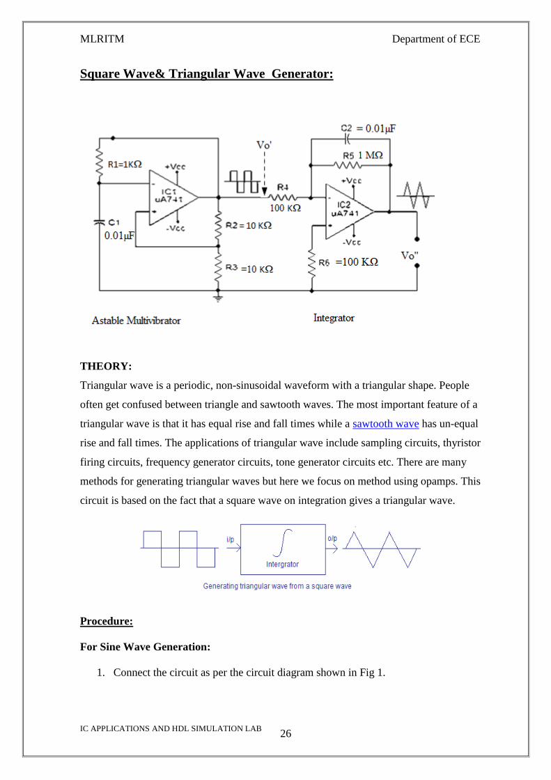
Square Wave& Triangular Wave Generator:
THEORY:
Triangular wave is a periodic, non-sinusoidal waveform with a triangular shape. People
often get confused between triangle and sawtooth waves. The most important feature of a
triangular wave is that it has equal rise and fall times while a sawtooth wave has un-equal
rise and fall times. The applications of triangular wave include sampling circuits, thyristor
firing circuits, frequency generator circuits, tone generator circuits etc. There are many
methods for generating triangular waves but here we focus on method using opamps. This
circuit is based on the fact that a square wave on integration gives a triangular wave.
Procedure:
For Sine Wave Generation:
1. Connect the circuit as per the circuit diagram shown in Fig 1.

MLRITM Department of ECE
IC APPLICATIONS AND HDL SIMULATION LAB
27
2. Give +12V, -12V and ground to circuit from power supply.
3. Observe the output on the CRO.
4. Calculate theoretical and practical output signal frequency and compare them.
For Square and Triangular Wave Generation:
1. Connect the circuit as per the circuit diagram shown in Fig 2.
2. Observe square wave at Vo’ and Triangular wave at Vo” as shown in figure 3.
3. Plot the waveforms on the graph sheet.
4. Calculate the frequency theoretically and compare them with the practical one.
PRECAUTIONS:
i. Check the circuit connections before switching on the power supply.
ii. Check the continuity of the connecting wires.
INFERENCE:
i. The working of oscillators is observed and the output is plotted.
ii. The frequency response of oscillator is plotted.
Applications:
1. Used in sine wave oscillators for audio frequencies.
2. Used in the application of function generators.
RESULT:
By using IC 741 the sine wave, Square wave and triangular wave forms are generated.
Review Questions:
1. What are the different ways of generating Sinusoidal waves?
2. What are different ways of generating square wave voltage waveforms?
3. What is phase-shift oscillator?
4. What is formula for frequency of oscillations for RC phase shift oscillator?
5. How a triangular wave can be generated?

MLRITM Department of ECE
IC APPLICATIONS AND HDL SIMULATION LAB
28
6. What is formula for frequency of oscillations for Astable square wave generator?
7. What is the frequency of oscillations of triangular wave when it is generated by
integrating the square wave?
8. For a circuit to act as an integrator, how the time constant has to be?
9. What is barkhausen criterion for oscillations?
10. Why three RC sections are used in the feedback for RC phase shift oscillator?
Exercise Problems:
1. Design an op-amp circuit to generate a sinusoidal waveform using 33KΩ, and
0.01µf capacitor and 3.3KΩ resistor.
2. Design an op-amp circuit to generate a square waveform.
3. Generate sinusoidal wave form by designing wein bridge oscillator using 741 op-
amp.
4. Generate sinusoidal wave form by designing RC Phase shift oscillator using 741
op-amp.
5. Generate a triangular wave form from square wave using 741 op-amps.
6. Generate a Saw tooth wave form from square wave using 741 op-amps.
7. Generate a Saw tooth wave form using 741 op-amps.
8. Design a single op-amp circuit to generate square, triangular and saw tooth wave
forms.
9. Design a square wave and triangular wave from a single circuit
10. Design a square wave by using 555 IC

MLRITM Department of ECE
IC APPLICATIONS AND HDL SIMULATION LAB
29
EXPERIMENT-5
MONOSTABLE AND ASTABLE MULTIVIBRATOR CIRCUITS
AIM: 1. To design a monostable multivibrator for a required pulse width using 555 timer.
2. To design astable multivibrator for a given frequency using 555 timer.
EQUIPMENT REQUIRED:
Bread board 1
CRO (20MHz) 1
IC 555 1
Resistors
47K 2
2.2K 1
10K 1
100K 1
Capacitors
0.01μF 2
0.1μF 2
PN Diode 1N4007 1
RPS 1
Function generator (10 Hz-20MHz) 1
Design:
Monostable Multivibrator:
T = 1.1R1C1
Let C1 = 0.01µF & R1 = 47K then T = 0.3ms(approx)
Astable Multivibrator:
For 55% duty cycle choose RB = 10K
THIGH = Tc = 0.693 (RA + RB)C
TLOW = Td = 0.693 RBC
T = THIGH + TLOW = 0.693 (RA + 2RB)C
f = 1/T = 1.44/ (RA + 2RB)C
% duty cycle, D = Tc / T * 100 = (RA + RB) / (RA + 2RB) * 100

MLRITM Department of ECE
IC APPLICATIONS AND HDL SIMULATION LAB
30
Circuit diagrams:
Monostable Multivibrator:
Triggering Circuit
Fig 1. Monostable Multivibrator
Astable Multivibrator:

MLRITM Department of ECE
IC APPLICATIONS AND HDL SIMULATION LAB
31
Fig 2. Astable Multivibrator
Procedure:
Monostable Multivibrator:
1. Connect the circuit as shown in the circuit diagram Fig 1.
2. Apply Negative triggering pulses of frequency 1 KHz at pin 2.
3. Observe the output waveform at pin 3 and measure capacitor voltage across it at
pin 6.
4. Theoretically calculate the pulse duration as T = 1.1R1C1
5. Compare it with experimental values.
6. Plot the graph for the input and output waveforms.
Astable Multivibrator:
1. Connect the circuit as shown in the circuit diagram Fig 2.
2. Observe the output waveform at pin 3 and measure capacitor voltage across it at
pin 6.
3. Theoretically calculate the Time period as T = 0.69 RBC + 0.69 (RA + RB)C.
4. Compare it with experimental values.
5. Plot the graph for the input and output waveforms.

MLRITM Department of ECE
IC APPLICATIONS AND HDL SIMULATION LAB
32
Model Wave Forms:
Monostable Multivibrator:
Waveforms at Capacitor and monostable output
Astable Multivibrator:

MLRITM Department of ECE
IC APPLICATIONS AND HDL SIMULATION LAB
33
PRECAUTIONS:
i.Check the circuit connections before switching on the power supply.
ii. Check the diode connection between pin 2 and 8
iii. Check the connections between pin no.1 and pin no.5
iv. Check the continuity of the connecting wires.
INFERENCE:
i. The working of 555 timer monostable multivibrator is observed and the output is
plotted.
ii. The time period of the output waveform is calculated.
iii. Frequency of the output wave form is calculated.
Applications:
i. To construct missing pulse detector circuit.
ii. To construct linear ramp generator circuit.
iii. To construct Frequency divider circuit.
RESULT: Designed and verified the waveforms of monostable multivibrator and Astable
multivibrator using 555 Timer.
.
REVIEW QUESTIONS:
1. Define duty cycle?
2. Draw the pin diagram of 555 timers?
3. What are the applications of 555 timers in monostable mode?
4. Explain capacitor output waveform in monostable mode?
5. Write down the expression for output pulse width in monostable mode?
6. Why the number has come for 555 IC as 555?

MLRITM Department of ECE
IC APPLICATIONS AND HDL SIMULATION LAB
34
7. Write down the expression for output pulse width in Astable mode?
8. What are the applications of 555 timers in Astable mode?
9. What is a quasi stable state and what is a steady state?.
10. What are the other names for the Monostable Multivibrator and Astable
Multivibrator?
Exercise Problems:
1. Design a astable multivibrator using 555 IC.
2. Design a monostable multivibrator using 555 IC.
3. Generate a square wave with 60% duty cycle using 555 IC.
4. Generate a square wave with variable duty cycle between 30% to 70%.
5. Design a multivibrator circuit using 555 IC to make the ON time of a bulb is 2sec
and OFF time is 1sec
6. Design a free running Oscillator using 555 IC.
7. Design a one short multivibrator using 555 IC.
8. Design a multivibrator circuit using 555 IC to make the ON time of a bulb is 1sec
and OFF time is 500msec.
9. Design a traffic signal controller with time delay of 30sec using 555IC.
10. Design a traffic signal Controller with time delay of 30sec and 45sec using 555 IC.

MLRITM Department of ECE
IC APPLICATIONS AND HDL SIMULATION LAB
35
EXPERIMENT-6
SCMITT TRIGGER CIRCUITS-USING IC741
AIM: To Design a Schmitt trigger circuit using IC 741 and verify the output wave forms.
EQUIPMENT REQUIRED:
Bread board 1 No.
Regulated power supply 1 No.
Function generator 1 No.
CRO 1 No.
IC 741 1 No.
Resistors
100K 2 No.s
100 2 No.s
1K 1 No.
10K 1 No.
5.1K 1 No.
Capacitor
0.01μF 2 No.s
Design: To design a Schmitt trigger for a given value of +Vsat, -Vsat, UTP and LTP.
+Vsat = Vcc - 3V (approx)
-Vsat = Vee + 3V (approx)
Select Vcc and Vee as per the design requirements.
UTP and LTP depends on β i.e. R2 / (R1 + R2). Select the resistors as per the UTP and LTP
requirements.
Design a Schmitt Trigger for +Vsat = 9V and -Vsat = - 6V and UTP and LTP as 3V and –
2V. For this requirement, Vcc = +12V and Vee = - 9V and the β = 1/3 ( R1 can be selected

MLRITM Department of ECE
IC APPLICATIONS AND HDL SIMULATION LAB
36
as 1K which gives R2 as 2K)
Circuit diagrams:
Fig 1. Schmitt trigger using IC 741
Procedure:
Using IC 741:
1. Connect the circuit as shown in fig 1(a) as Schmitt trigger using IC 741.
2. Give a 5 Vp-p sine wave of 1 kHz as input.
3. Observe the wave form on CRO and measure UTP and LTP, Vsat and - Vsat.
4. Use X-Y mode in CRO and observe hysteresis curve.

MLRITM Department of ECE
IC APPLICATIONS AND HDL SIMULATION LAB
37
5. Repeat the above experiment for R1 = 5.1Kohms and 15 Kohms and observe the
effect.
Expected waveforms:
(a) Input wave form (b) output wave form
Observations:
Parameter
Input
Output
Voltage(Vp-p), V
Time period - Positive Half
cycle(ms)
Time period -
Negative Half
cycle(ms)
Theoretical Observed
UTP
LTP
PRECAUTIONS:
i. Check the circuit connections before switching on the power supply.
ii. Pin No.1 and Pin No.8 should be left free.
iii. Check the continuity of the connecting wires.

MLRITM Department of ECE
IC APPLICATIONS AND HDL SIMULATION LAB
38
INFERENCE:
i. The working of Schmitt Trigger is observed and the output is plotted.
ii. The upper and lower Threshold voltages are measured.
Applications:
i. This can be used as frequency divider, pulse width modulator, burglar alarm, FSK
generator, ramp generator, pulse position modulator, waveform generator, etc.
ii.This can be used as square wave converter.
Result: Designed and verified Schmitt trigger circuit using IC 741.
VIVA Questions:
1. What are the circuits used to generate square wave?
2. Short notes on zero crossing detector?
3. Define hysteresis width?
4. What are the other names for Schmitt Trigger?
5. What is the duty cycle of the output square wave of the Schmitt Trigger?
6. What is a Schmitt Trigger?
7. For what requirements, Schmitt Trigger is used?
8. define utp and ltp. what are the values of utp and ltp for the above circuit?
9. what is the basic difference between the comparator and schmitt trigger?
10. which type of feedback is used in schmitt trigger?
Viva Questions:
1. Schmitt trigger is also known as?
2. What is the disadvantage of comparator and how it is overcome?
3. Define hysteresis.
4. What are the Applications of schitt trigger?
5. Define UTP.
6. Define LTP.

MLRITM Department of ECE
IC APPLICATIONS AND HDL SIMULATION LAB
39
7. Which type of feedback is used in Schmitt trigger?
8. What is the other name of hysteresis?
9. Write the formula for hysteresis
10. Draw the schematic diagram of 555 as Schmitt trigger.
Exercise Problems:
1. Design single supply Schmitt trigger circuit.
2. Design Schmitt trigger with Vcc=5V, VLow=0V, VHigh=5V, VTL=3.5V,
VTh=5V.
3. Design Schmitt trigger with VTL=2V, VTh=5V.
4. In Schmitt trigger circuit if Vin exceeds Vsat what will happen.
5. In Schmitt trigger when Vin>Vsat output is distorted or not if distorted why?
6. Design Schmitt trigger with Vcc=5V, VLow=0V, VHigh=5V, VTL=2.25V,
VTh=5V.
7. Design Schmitt trigger with VTL=1.5v, VTh=4V.
8. Design Schmitt trigger with Vcc=5V, VLow=0v, VHigh=6v, Vth=6V.
MLRITM Department of ECE
IC APPLICATIONS AND HDL SIMULATION LAB
40
EXPERIMENT-7
IC 565 – PLL APPLICATIONS
AIM:
To study the operation of NE565 PLL – with a given free running frequency.
EQUIPMENT REQUIRED:
DC power supply
CRO
Bread Board
Function Generator
Resistors 2.2kΩ, 10KΩ, 18KΩ – 1No. each
Capacitor 10µF – 1No
Capacitor 0.001µF – 2Nos
IC565 - 1No.
THEORY:
The 565 IC is available as a14-pin DIP package. The output frequency of the VCO
is fo = 1.2 /4 RTCT, where RT and CT are the external Resistor and Capacitor connected to
pin 8 and pin 9. A value between 2k and 20k is recommended for RT. The VCO free
running frequency is adjusted with RT and CT, so that it is at the centre of the input
frequency range.
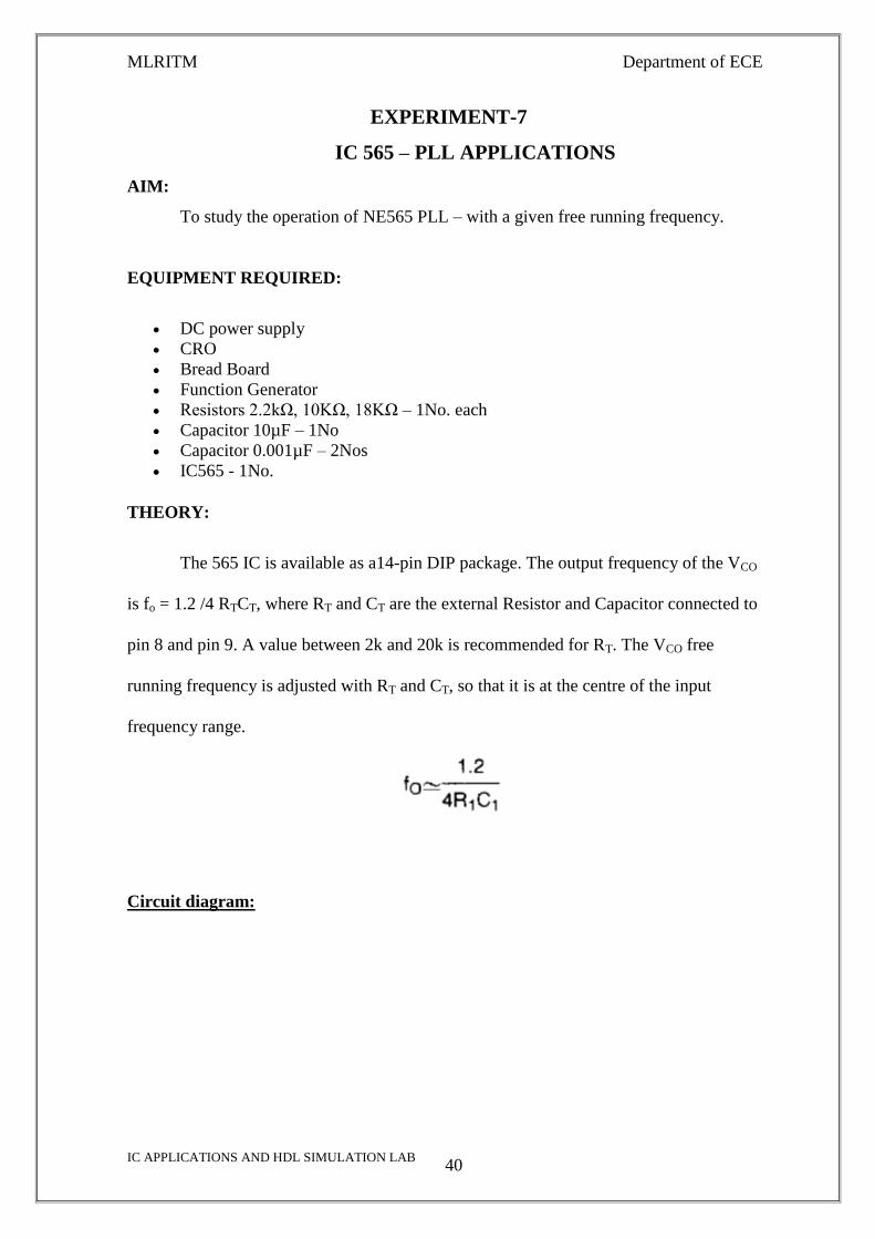
Circuit diagram:

MLRITM Department of ECE
IC APPLICATIONS AND HDL SIMULATION LAB
41
Procedure:
1. Connect the circuit as shown in the figure.
2. Measure the free running frequency of VCO at pin 4 with the input signal Vin =
zero. Compare it with the calculated value = 1.2/4RTCT
3. Now apply the input signal of 1Vpp square wave of 100Hz to pin 2. Connect
channel 1 of the CRO to pin 2 and display this signal on the scope.
4. Gradually increase the input frequency till the PLL is locked to the input
frequency.
5. This frequency fCL gives the lower end of the capture range.
6. Go on increase the input frequency, till PLL stops tracking the input signal. This
frequency fLH gives the upper end of the lock range.
7. If the input frequency is increased further the loop will be in unlocked condition
only.
8. Now gradually decrease the input frequency till the PLL is again get locked. This
is the frequency fCH, the upper end of the capture range. Keep on decreasing the

MLRITM Department of ECE
IC APPLICATIONS AND HDL SIMULATION LAB
42
input frequency until the loop is unlocked. This frequency fLL gives the lower end
of the lock range.
Expected Wave Forms:

MLRITM Department of ECE
IC APPLICATIONS AND HDL SIMULATION LAB
43
PRECAUTIONS:
i. Check the circuit connections before switching on the power supply.
ii. Check the connection between pin 7 and 8
iii. Check the connections at the input.
iv. Check the continuity of the connecting wires
INFERENCE:
i. The working of 565 PLL is observed and the output is plotted.
ii. The time period of the output waveform is calculated
iii. Frequency of the output wave form is calculated
iv.The Lock range and Capture range of the PLL are calculated.
PRECAUTIONS:
i. Check the circuit connections before switching on the power supply.
ii. Check the connection between pin 7 and 8
iii. Check the connections at the input.
iv. Check the continuity of the connecting wires.
Applications:
i.To construct missing frequency multiplier circuit
ii. To construct AM demodulator circuit
iii. To construct FSK demodulator circuit
RESULT:
fO Free running frequency: ____________
fLL Lower Locking frequency: ____________
fCL Lower capture frequency: ____________
fCH Higher capture frequency: ____________
fLH Higher Locking frequency: ____________

MLRITM Department of ECE
IC APPLICATIONS AND HDL SIMULATION LAB
44
VIVA Questions:
1. What are the basic blocks of a PLL?
2. Define VCO?
3. What is the formula for the free running frequency Fo of 565 PLL?
4. What is PLL?
5. Define lock range?.
6. Define pull-in time?
7. Define capture range?
8. What is the function of the LPF in PLL?
9. What are the applications of PLL?
10. Which is greater – lock in range or capture range?

MLRITM Department of ECE
IC APPLICATIONS AND HDL SIMULATION LAB
45
EXPERIMENT-8
VOLTAGE REGULATOR USING IC723
AIM: To study the voltage regulation characteristics and plot the response curve for line
regulation and load regulation using 723 IC.
APPARATUS:
1. Bread board
2. IC LM723 - 1No.
3. Resistors(1KΩ, 2.7KΩ, 4.7KΩ, 6.8KΩ) - 1No. each
4. RPS
5. DRB / Potentiometer 10K - 1No.
6. Capacitors 100pF - 1No.
7. Connecting wires
8. Ammeter 0-20 mA - 1No.
9. Voltmeter 0-20V - 1No.
Circuit Diagrams:
a. To get output voltage > 7V

MLRITM Department of ECE
IC APPLICATIONS AND HDL SIMULATION LAB
46
b. To get output voltage < 7V
PROCEDURE:
I. LINE REGULATION
1. Connections are made as per the circuit diagram.
2. RPS is connected as Vi.
3. A fixed load of 1K is kept at the output.
4. Input Vi is varied from 15V to 25V in steps of 2V and Output voltage is measured.
5. Graph is drawn between the input voltage and output voltage.
II. LOAD REGULATION
1. Connections are made as per the circuit diagram.
2. RPS is connected as Vi.
3. Output voltage is measured by varying the load (Potentiometer), in steps of 1mA
4. Graph is drawn between the output voltage and output current (load).
Observations:
Line regulation = (ΔVout / ΔVin) / 100%
Vnl =

MLRITM Department of ECE
IC APPLICATIONS AND HDL SIMULATION LAB
47
Line Voltage (V) Output Voltage (V)
Load regulation
Regulated
Output (V)
Load
Current(mA)
Load
Resistance(KΩ)
Load
Regulation
Regulation = [(Vnl - Vfl) / Vfl] * 100%
Model Graph:

MLRITM Department of ECE
IC APPLICATIONS AND HDL SIMULATION LAB
48
INFERENCE:
i. The working of 723 regulator is observed and the output is plotted.
ii. The load regulation is calculated.
iii. The line regulation is calculated.
PRECAUTIONS:
i.Check the circuit connections before switching on the power supply.
ii. Check the continuity of the connecting wires.
Result: The load regulations and line regulations are observed by the IC 723.

MLRITM Department of ECE
IC APPLICATIONS AND HDL SIMULATION LAB
49
Experiment 8B
AIM: To study the voltage regulation characteristics and plot the response curve for line
regulation and load regulation using 7805, 7809, 7912 ICs.
Apparatus:
1. Bread board
2. ICs 7805, 7809, 7912 ICs - 1No. each
3. RPS
4. DRB / potentiometer 10KΩ - 1No.
5. Capacitors 1000µF, 22 µF - 1No. each
6. Voltmeter - 0-20V
7. Connecting wires
Circuit Diagrams:
Figure.1 Fixed Positive Voltage regulator
Figure.2 Fixed Negative Voltage Regulator

MLRITM Department of ECE
IC APPLICATIONS AND HDL SIMULATION LAB
50
Theory: A regulated power supply has to provide constant output voltage irrespective of
variation in the load connected to the power supply or variation in the input unregulated
power given to the power supply. This is achieved by taking the feedback from the output
voltage and compared with a fixed reference voltage. Based on the error, the output
voltage is adjusted.
Procedure:
For fixed positive voltage regulator (7805 and 7809):
1. Connect the circuit diagram as shown in figure.1.
2. Apply the unregulated voltage to the IC 7805 and note down the regulator output
voltage. Vary input voltage from 7V to 20V and record the output voltages.
3. Calculate the line regulation of the regulator using the formula.
4. Line Regulation = ΔVO /ΔVi.
5. Now, fix the input voltage as 15V and vary the load resistance RL, from 1K to 10
K ohms. Note down the regulator output voltage.
6. Calculate the Load regulation of the regulator using the formula.
7. Load Regulation =ΔVO / ΔIL.
8. Repeat the above procedure for 7809.
For fixed negative voltage regulator (7912):
1. Connect the circuit diagram as shown in figure.2.
2. Apply the unregulated voltage to the IC 7912 and note down the regulator output
voltage.
3. Vary input voltage from 7V to 20V and record the output voltages.
4. Calculate the line regulation of the regulator using the formula.
5. Line Regulation = ΔVO / ΔVi.
6. Now, fix the input voltage as 15V and vary the load resistance RL, from 1K to 10
K ohms. Note down the regulator output voltage.
7. Calculate the Load regulation of the regulator using the formula.
8. Load Regulation =ΔVO / ΔIL.
Observations:
1). For +Ve Voltage Regulator 7805
Line Regulation: (RL is constant)

MLRITM Department of ECE
IC APPLICATIONS AND HDL SIMULATION LAB
51
S.No. Unregulated DC
Input, Vi in Volts
Regulated DC
Output, VO in
Volts
Load Regulation: (Vi is constant)
S.No. Load Resistance,
RL in Ohms Regulated DC
output, VO in Volts
2). For +Ve Voltage Regulator 7809
Line Regulation: (RL is constant)
S.No. Unregulated DC Input,
Vi in Volts
Regulated DC
Output, VO in
Volts
Load Regulation: (Vi is constant)

MLRITM Department of ECE
IC APPLICATIONS AND HDL SIMULATION LAB
52
S.No. Load Resistance, RL in Ohms Regulated DC output,
VO in Volts
3). For -Ve Voltage Regulator 7912
Line Regulation: (RL is constant)
S.No. Unregulated DC Input,
Vi in Volts Regulated DC
Output, VO in Volts
Load Regulation: (Vi is constant)
S.No. Load Resistance, RL in Ohms Regulated DC
output, VO in Volts

MLRITM Department of ECE
IC APPLICATIONS AND HDL SIMULATION LAB
53
Model Graphs(for +Ve Voltage Regulators):
Fig 3. Line Regulation
Fig 4. Load Regulation
Model Graphs(for -Ve Voltage Regulator):

MLRITM Department of ECE
IC APPLICATIONS AND HDL SIMULATION LAB
54
Figure 5. Line Regulation for 79XX
Figure 6. Load Regulation for 79XX
PRECAUTIONS:
i. Check the circuit connections before switching on the power supply.
ii. Check the continuity of the connecting wires.
INFERENCE:
i. The working of 78XX regulator is observed and the output is plotted.
ii. The load regulation is calculated.
iii. The line regulation is calculated.
Applications:

MLRITM Department of ECE
IC APPLICATIONS AND HDL SIMULATION LAB
55
i. Used as an fixed voltage regulator.
ii. Used as an current source.
Result:
Studied the 3-terminal fixed voltage regulator using IC 78XX and 79XX series &also the
line regulation and load regulation of them are verified.
VIVA Questions:
1. What is meant by line regulation?
2. What is meant by load regulation?
3. What is the function of a series pass transistor in Linear regulated power supply?
4. What is a voltage regulator?
5. What are the advantages of IC voltage regulators?
6. What is meant by current limiting?
7. Give the drawbacks of linear regulators.
8. What is thermal shut down?
9. What are the limitations of 3 pin fixed voltage regulators?
10. How current boosting is achieved in 723 IC?

MLRITM Department of ECE
IC APPLICATIONS AND HDL SIMULATION LAB
56
Part-II
LIST OF EXPERIMENTS
1. HDL code to realize all the logic gates
1.1. Logic Gates (Data Flow Model)
1.2. Logic Gates (Behavioral Model)
1.3. Nand Logic Gate (Structural Model)
1.4. Nor Logic Gate (Structural Model)
1.5. XNor Logic Gate (Structural Model)
2. Design of 2-to-4 decoder
3. Design of 8-to-3 encoder
3.1. Without parity
3.2 .With parity
4. Design of 8-to-1 multiplexer
5. Design of 4 bit binary to gray converter
6. Design of 4-bit Comparator
7. Design of full adder using 3 modeling styles
7.1. Full adder (dataflow Model)
7.2. Full adder (Behavioral Model)
7.3. Full adder (Behavioral Model with Select)
7.4. Full adder (Structural Model)
8. Design of flip flops: SR,D,JK,T
8.1. SR flip flop
8.2. D flip flop
8.3. JK flip flop
8.4. T flip flop
9. Design of 4-bit binary, BCD counters (synchronous/ asynchronous reset)
9.1. 4-bit synchronous counter
9.2. 4-bit asynchronous counter
9.3. BCD up counter
9.4. BCD down counter
10. Finite state machine design

MLRITM Department of ECE
IC APPLICATIONS AND HDL SIMULATION LAB
57
1.1 Logic Gates (Data Flow Model)
Aim: To design all types the logic gates using HDL Programming and verify
their simulation and synthesis reports.
Apparatus:
Personal Computer: 1 No
Operating System : Windows XP,
Software : Xilinx 9.2i.
Theory:
A logic gate performs a logical operation on one or more logic inputs and produces a
single logic output. The logic is normally performed as Boolean logic and is most
commonly found in digital circuits.
The different types of logic gates are:
i. AND gate
The AND gate is an electronic circuit that gives a high output (1) only if all its inputs
are high. A dot (.) is used to show the AND operation i.e. A.B. Bear in mind that this
dot is sometimes omitted i.e. AB
ii. OR gate
The OR gate is an electronic circuit that gives a high output (1) if one or more of its
inputs are high. A plus (+) is used to show the OR operation.
iii. NOT gate

MLRITM Department of ECE
IC APPLICATIONS AND HDL SIMULATION LAB
58
The NOT gate is an electronic circuit that produces an inverted version of the input at
its output. It is also known as an inverter. If the input variable is A, the inverted output
is known as NOT A. This is also shown as A', or A with a bar over the top, as shown
at the outputs. The diagrams below show two ways that the NAND logic gate can be
configured to produce a NOT gate. It can also be done using NOR logic gates in the
same way.
iv. NAND gate
This is a NOT-AND gate which is equal to an AND gate followed by a NOT gate.
The outputs of all NAND gates are high if any of the inputs are low. The symbol is an
AND gate with a small circle on the output. The small circle represents inversion.
v. NOR gate
This is a NOT-OR gate which is equal to an OR gate followed by a NOT gate. The
outputs of all NOR gates are low if any of the inputs are high.

MLRITM Department of ECE
IC APPLICATIONS AND HDL SIMULATION LAB
59
The symbol is an OR gate with a small circle on the output. The small circle
represents inversion.
vi. EXOR gate
The 'Exclusive-OR' gate is a circuit which will give a high output if either, but not
both, of its two inputs are high. An encircled plus sign () is used to show the EOR
operation.
vii. EXNOR gate
The 'Exclusive-NOR' gate circuit does the opposite to the EOR gate. It will give a low
output if either, but not both, of its two inputs are high. The symbol is an EXOR gate
with a small circle on the output. The small circle represents inversion.
Block Diagram:
Program:
library IEEE;
use IEEE.STD_LOGIC_1164.ALL;
use IEEE.STD_LOGIC_ARITH.ALL;

MLRITM Department of ECE
IC APPLICATIONS AND HDL SIMULATION LAB
60
use IEEE.STD_LOGIC_UNSIGNED.ALL;
entity allall is
Port ( a : in STD_LOGIC;
b : in STD_LOGIC;
c : out STD_LOGIC;
d : out STD_LOGIC;
e : out STD_LOGIC;
f : out STD_LOGIC;
g : out STD_LOGIC;
h : out STD_LOGIC;
i : out STD_LOGIC);
end allall;
architecture dataflow of allall is
begin
c<= a and b;
d<= a or b;
e<= not a;
f<= a nand b;
g<= a nor b;
h<= a xor b;
i<= a xnor b;
end dataflow;
Simulation Waveform:
Synthesis Report:
==================================================================
=========
* Final Report *
==================================================================
=========
Cell Usage :
# BELS : 7
# AND2 : 1
# INV : 4
# OR2 : 1
# XOR2 : 1
# IO Buffers : 9

MLRITM Department of ECE
IC APPLICATIONS AND HDL SIMULATION LAB
61
# IBUF : 2
# OBUF : 7
==================================================================
=========
RTL Schematic:

MLRITM Department of ECE
IC APPLICATIONS AND HDL SIMULATION LAB
62
1.2 Logic Gates (Behavioral Model)
Aim: To simulate and verify the All Logic Gates with Behavioral Model
Apparatus:
Personal Computer:1 No
Operating System : Windows XP,
Software : Xilinx 9.1i.
Program:
library IEEE;
use IEEE.STD_LOGIC_1164.ALL;
use IEEE.STD_LOGIC_ARITH.ALL;
use IEEE.STD_LOGIC_UNSIGNED.ALL;
entity allbeh is
Port ( a : in STD_LOGIC;
b : in STD_LOGIC;
c,d,e,f,g,h,i : out STD_LOGIC);
end allbeh;
architecture Behavioral of allbeh is
begin
process (a,b)
begin
if a='1' and b='1' then c<='1';
else c<='0';
end if;
if a='0' and b='0' then d<='0';
else d<='1';
end if;
if a='1' and b='1' then e<='0';
else e<='1';
end if;
if a='0' and b='0' then f<='1';
else f<='0';
end if;
if a=b then g<='0';
else g<='1';
end if;
if a=b then h<='1';
else h<='0';
end if;
if a='0' then i<='1';
else i<='0';
end if;
end process;
end Behavioral;
Simulation Waveform:

MLRITM Department of ECE
IC APPLICATIONS AND HDL SIMULATION LAB
63
Synthesis Report:
==================================================================
=========
* Final Report *
==================================================================
=========
Cell Usage :
# BELS : 9
# AND2 : 2
# INV : 6
# XOR2 : 1
# IO Buffers : 9
# IBUF : 2
# OBUF : 7
=============================================================
==============
RTL Schematic:

MLRITM Department of ECE
IC APPLICATIONS AND HDL SIMULATION LAB
64
1.3 Nand Logic Gate (Structural Model)
Aim: To simulate and verify the Nand Gate with Structural Model
Apparatus:
Personal Computer:1 No
Operating System : Windows XP,
Software : Xilinx 9.1i.
Program:
library IEEE;
use IEEE.STD_LOGIC_1164.ALL;
use IEEE.STD_LOGIC_ARITH.ALL;
use IEEE.STD_LOGIC_UNSIGNED.ALL;
entity nandstruct is
Port ( x : in STD_LOGIC;
y : in STD_LOGIC;
z : out STD_LOGIC);
end nandstruct;
architecture structural of nandstruct is
component and12 is
port(a,b:in std_logic;
c:out std_logic);
end component;
component not12 is
port(d:in std_logic;
e:out std_logic);
end component;
signal w:std_logic;
begin
a1:and12 port map(x,y,w);
a2:not12 port map(w,z);
end structural;
-- program for and12
library IEEE;
use IEEE.STD_LOGIC_1164.ALL;
use IEEE.STD_LOGIC_ARITH.ALL;
use IEEE.STD_LOGIC_UNSIGNED.ALL;
entity and12 is
Port ( a : in STD_LOGIC;
b : in STD_LOGIC;
c : out STD_LOGIC);
end and12;
architecture dataflow of and12 is
begin
c<=a and b;
end dataflow;
-- program for not12

MLRITM Department of ECE
IC APPLICATIONS AND HDL SIMULATION LAB
65
library IEEE;
use IEEE.STD_LOGIC_1164.ALL;
use IEEE.STD_LOGIC_ARITH.ALL;
use IEEE.STD_LOGIC_UNSIGNED.ALL;
entity not12 is
Port ( d : in STD_LOGIC;
e : out STD_LOGIC);
end not12;
architecture dataflow of not12 is
begin
e<= not d;
end dataflow;
Simulation Waveform:
Synthesis Report:
==================================================================
=========
* Final Report *
==================================================================
=========
Cell Usage :
# BELS : 3
# INV : 2
# OR2 : 1
# IO Buffers : 3
# IBUF : 2
# OBUF : 1
==================================================================
=========

MLRITM Department of ECE
IC APPLICATIONS AND HDL SIMULATION LAB
66
RTL Schematic:

MLRITM Department of ECE
IC APPLICATIONS AND HDL SIMULATION LAB
67
1.4 Nor Logic Gate (Structural Model)
Aim: To simulate and verify the Nor Gate with Structural Model
Apparatus:
Personal Computer:1 No
Operating System : Windows XP,
Software : Xilinx 9.1i.
Program:
library IEEE;
use IEEE.STD_LOGIC_1164.ALL;
use IEEE.STD_LOGIC_ARITH.ALL;
use IEEE.STD_LOGIC_UNSIGNED.ALL;
entity norstruct is
Port ( x : in STD_LOGIC;
y : in STD_LOGIC;
z : out STD_LOGIC);
end norstruct;
architecture structural of norstruct is
component or12 is
port(a,b:in std_logic;
c:out std_logic);
end component;
component not12 is
port(d:in std_logic;
e:out std_logic);
end component;
signal w:std_logic;
begin
a1:or12 port map(x,y,w);
a2:not12 port map(w,z);
end structural;
-- program for or12
library IEEE;
use IEEE.STD_LOGIC_1164.ALL;
use IEEE.STD_LOGIC_ARITH.ALL;
use IEEE.STD_LOGIC_UNSIGNED.ALL;
entity or12 is
Port ( a : in STD_LOGIC;
b : in STD_LOGIC;
c : out STD_LOGIC);
end or12;
architecture dataflow of or12 is
begin
c<=a or b;
end dataflow;

MLRITM Department of ECE
IC APPLICATIONS AND HDL SIMULATION LAB
68
-- program for not12
library IEEE;
use IEEE.STD_LOGIC_1164.ALL;
use IEEE.STD_LOGIC_ARITH.ALL;
use IEEE.STD_LOGIC_UNSIGNED.ALL;
entity not12 is
Port ( d : in STD_LOGIC;
e : out STD_LOGIC);
end not12;
architecture dataflow of not12 is
begin
e<= not d;
end dataflow;
Simulation Waveform:
Synthesis Report:
==================================================================
=========
* Final Report *
==================================================================
=========
Cell Usage :
# BELS : 3
# AND2 : 1
# INV : 2
# IO Buffers : 3
# IBUF : 2
# OBUF : 1
=============================================================
==============
RTL Schematic:
MLRITM Department of ECE
IC APPLICATIONS AND HDL SIMULATION LAB
69

MLRITM Department of ECE
IC APPLICATIONS AND HDL SIMULATION LAB
70
1.5 XNor Logic Gate (Structural Model)
Aim: To simulate and verify the XNor Gate with Structural Model
Apparatus:
Personal Computer:1 No
Operating System : Windows XP,
Software : Xilinx 9.1i.
Program:
library IEEE;
use IEEE.STD_LOGIC_1164.ALL;
use IEEE.STD_LOGIC_ARITH.ALL;
use IEEE.STD_LOGIC_UNSIGNED.ALL;
entity xnors is
Port ( x : in STD_LOGIC;
y : in STD_LOGIC;
z : out STD_LOGIC);
end xnors;
architecture struct of xnors is
component xor12 is
port(a,b:in std_logic;
c:out std_logic);
end component;
component not12 is
port ( d : in STD_LOGIC;
e : out STD_LOGIC);
end component;
signal w:std_logic;
begin
a1:xor12 port map (x,y,w);
a2:not12 port map (w,z);
end struct;
-- program for xor12
library IEEE;
use IEEE.STD_LOGIC_1164.ALL;
use IEEE.STD_LOGIC_ARITH.ALL;
use IEEE.STD_LOGIC_UNSIGNED.ALL;
entity xor12 is
Port ( a : in STD_LOGIC;
b : in STD_LOGIC;
c : out STD_LOGIC);
end xor12;
architecture dataflow of xor12 is
begin
x<=p xor q;
end dataflow;

MLRITM Department of ECE
IC APPLICATIONS AND HDL SIMULATION LAB
71
-- program for not12
library IEEE;
use IEEE.STD_LOGIC_1164.ALL;
use IEEE.STD_LOGIC_ARITH.ALL;
use IEEE.STD_LOGIC_UNSIGNED.ALL;
entity not12 is
Port ( d : in STD_LOGIC;
e : out STD_LOGIC);
end not12;
architecture dataflow of not12 is
begin
e<= not d;
end dataflow;
Simulation Waveform:
Synthesis Report:
==================================================================
=========
* Final Report *
==================================================================
=========
Cell Usage :
# BELS : 2
# INV : 1
# XOR2 : 1
# IO Buffers : 3
# IBUF : 2
# OBUF : 1
==================================================================
=========
RTL Schematic:

MLRITM Department of ECE
IC APPLICATIONS AND HDL SIMULATION LAB
72
Result: Designed and verified logic gates using HDL.
Viva Questions
1. How many N AND gates are required to design XOR logic?
2. How many NOR gates are required to design XOR logic?
3. How many N AND gates are required to design XNOR logic?
4. How many NOR gates are required to design XNOR logic?
5. Draw the circuit of AND gate using Transistors.
6. Draw the circuit of OR gate using Transistors.
7. Draw the circuit of NOT gate using Transistors.
8. Define Fan-in Fan Out.
9. Define Noise Margin.
10. Define Figure of merit.

MLRITM Department of ECE
IC APPLICATIONS AND HDL SIMULATION LAB
73
EXERCISE PROBLEMS
1. To simulate and verify 3-input AND gate with dataflow model.
2. Write a VHDL code for 2-input NOR gate in structural model and verify it.
3. To simulate and verify 3-input OR gate with dataflow model.
4. Write a VHDL code for 3-input NAND gate in structural model and verify it.
5. To simulate and verify 2-input NAND gate with behavioral model.
6. To simulate and verify 2-input NOR gate with behavioral model.
7. Write VHDL code for 3-input NAND gate in dataflow model and verify it.
8. Write VHDL code for 3-input NOR gate in dataflow model and verify it.
9. To simulate and verify 3-input AND gate with behavioral model.
10 To simulate and verify 3-input OR gate with behavioral model.
11 Write a VHDL code for 3-input NAND gate in behavioral model and verify it.
12 To simulate and verify 2input NAND gate with data flow model
13 Write a VHDL code for 2-input NAND gate in Structural model and verify it.
14 To simulate and verify 2input NOR gate with data flow model
15 Write a VHDL code for 3-input NOR gate in behavioral model and verify it
16 Write a VHDL code for 2-input XOR gate in data flow model and verify it
17 Write a VHDL code for 2-input XOR gate in behavioral model and verify it
18 Write a VHDL code for 2-input XNOR gate in data flow model and verify it
19 Write a VHDL code for 2-input XNOR gate in behavioral model and verify it
20 Write a VHDL code for 2-input XNOR gate in Structural model and verify it

MLRITM Department of ECE
IC APPLICATIONS AND HDL SIMULATION LAB
74
2. Design of 2-to-4 decoder
Aim: To design 2 to 4 line decoder using HDL, obtain the simulation and
synthesis.
Apparatus:
Personal Computer: 1 No.
Operating System : Windows XP.
Software : Xilinx 9.2i.
Theory:
Decoders are circuits with two or more inputs and 2n outputs. Based on the input
code, only one of the output is selected.
The truth table of 2-to-4 line decoder is
Developed into a circuit it looks like
Figure: Gate Level Representation of 2 to 4 Line Decoder (Logic Diagram)

MLRITM Department of ECE
IC APPLICATIONS AND HDL SIMULATION LAB
75
Block Diagram:
Program:
library IEEE;
use IEEE.STD_LOGIC_1164.ALL;
use IEEE.STD_LOGIC_ARITH.ALL;
use IEEE.STD_LOGIC_UNSIGNED.ALL;
entity dec24 is
port(a,b,e:in std_logic;
z:out std_logic_vector(0 to 3));
end dec24;
architecture data of dec24 is
begin
z(0)<= (not a) and (not b) and e;
z(1)<= b and (not a) and e;
z(2)<= a and (not b) and e;
z(3)<= a and b and e;
end data;

MLRITM Department of ECE
IC APPLICATIONS AND HDL SIMULATION LAB
76
Simulation Waveform:
Synthesis Report:
==================================================================
=========
* Final Report *
==================================================================
=========
Cell Usage :
# BELS : 10
# AND2 : 4
# AND3 : 2
# INV : 4
# IO Buffers : 7
# IBUF : 3
# OBUF : 4
==================================================================
=========
RTL Schematic:

MLRITM Department of ECE
IC APPLICATIONS AND HDL SIMULATION LAB
77
Result: Designed 2x4 decoder and verified by synthesizing and simulating the code.
Viva Questions
1. Define Decoder ?
2. What are the applications of decoder?
3. What is the difference between decoder and encoder?
4. What is the difference between encoder and priority encoder ?
5. How may 2 to 4 decoders are required to construct 4 to 16 decoder ?
6. What is the IC no of dual 2 to 4 decoder ?
7. What is the IC no of 3 to8 decoder ?
8. What are the advantages of decoder ?
9. What is the IC no of dual 2 to 4 decoder ?
10. What is the IC no of 3 to 8 decoder ?

MLRITM Department of ECE
IC APPLICATIONS AND HDL SIMULATION LAB
78
EXERCISE PROBLEMS
1. Design 4 to 16 decoder using 2 to 4 decoder
2. Write VHDL code foe 2 to 4 decoder in structural model and verify it.
3. To simulate and verify the 3 to 8 line decoder with dataflow model.
4. To simulate and verify the 4 to 16 line decoder with dataflow model.
5. Write a VHDL code for 3 to 8 line decoder in behavioral model and verify it.
6. Write a VHDL code for 3 to 8 line decoder in data flow model and verify it.
7. Write a VHDL code for 2 to 4 line decoder in behavioral model and verify it.
8. Write a VHDL code for 2 to 4 line decoder in data flow model and verify it.
9. Write a VHDL code for 4 to 16 line decoder in data flow model and verify it.
10. Write a VHDL code for 4 to 16 line decoder in behavioral model and verify it.
11. Write a VHDL code for 4 to 16 line decoder in structural model and verify it.
12. Write a VHDL code for 5 to 32 line decoder in data flow model and verify it.
13. Write a VHDL code for 5 to 32 line decoder in behavioral model and verify it.
14. Write a VHDL code for 5 to 32 line decoder in structural model and verify it.
15. Design 5 to 32 decoder using 2 to 4 decoder

MLRITM Department of ECE
IC APPLICATIONS AND HDL SIMULATION LAB
79
3.1 Design of 8-to-3 Encoder (Without Priority)
Aim: To Design and verify the functionality of 8 to 3 Encoder.
Apparatus:
Personal Computer: 1 No
Operating System : Windows XP,
Software : Xilinx 9.2i.
Theory:
An Encoder is a device, circuit, transducer, software program, algorithm or person
that converts information from one format or code to another. The purpose of encoder
is standardization, speed, secrecy, security, or saving space by shrinking size.
Encoders are combinational logic circuits and they are exactly opposite of decoders.
They accept one or more inputs and generate a multibit output code.
Encoders perform exactly reverse operation than Decoder. An Encoder has M input
and N output lines. Out of M input lines only one is activated at a time and produces
equivalent code on output N lines. If a device output code has fewer bits than the
input code has, the device is usually called an encoder.
Octal to binary encoder
Octal-to-Binary take 8 inputs and provides 3 outputs, thus doing the opposite of what
the 3-to-8 decoder does. At any one time, only one input line has a value of 1. The
figure below shows the truth table of an Octal-to-binary encoder.
Inputs Outputs
D0 D1 D2 D3 D4 D5 D6 D7 E2 E1 E0 1 0 0 0 0 0 0 0 0 0 0
0 1 0 0 0 0 0 0 0 0 1
0 0 1 0 0 0 0 0 0 1 0
0 0 0 1 0 0 0 0 0 1 1
0 0 0 0 1 0 0 0 1 0 0
0 0 0 0 0 1 0 0 1 0 1
0 0 0 0 0 0 1 0 1 1 0
0 0 0 0 0 0 0 1 1 1 1

MLRITM Department of ECE
IC APPLICATIONS AND HDL SIMULATION LAB
80
Table: Truth Table of octal to binary encoder
For an 8-to-3 binary encoder with inputs I0-I7 the logic expressions of the outputs
Y0-Y2 are:
E0 = I1 + I3 + I5 + I7
E1= I2 + I3 + I6 + I7
E2 = I4 + I5 + I6 +I7
Fig. Logic Diagram of octal to binary encoder
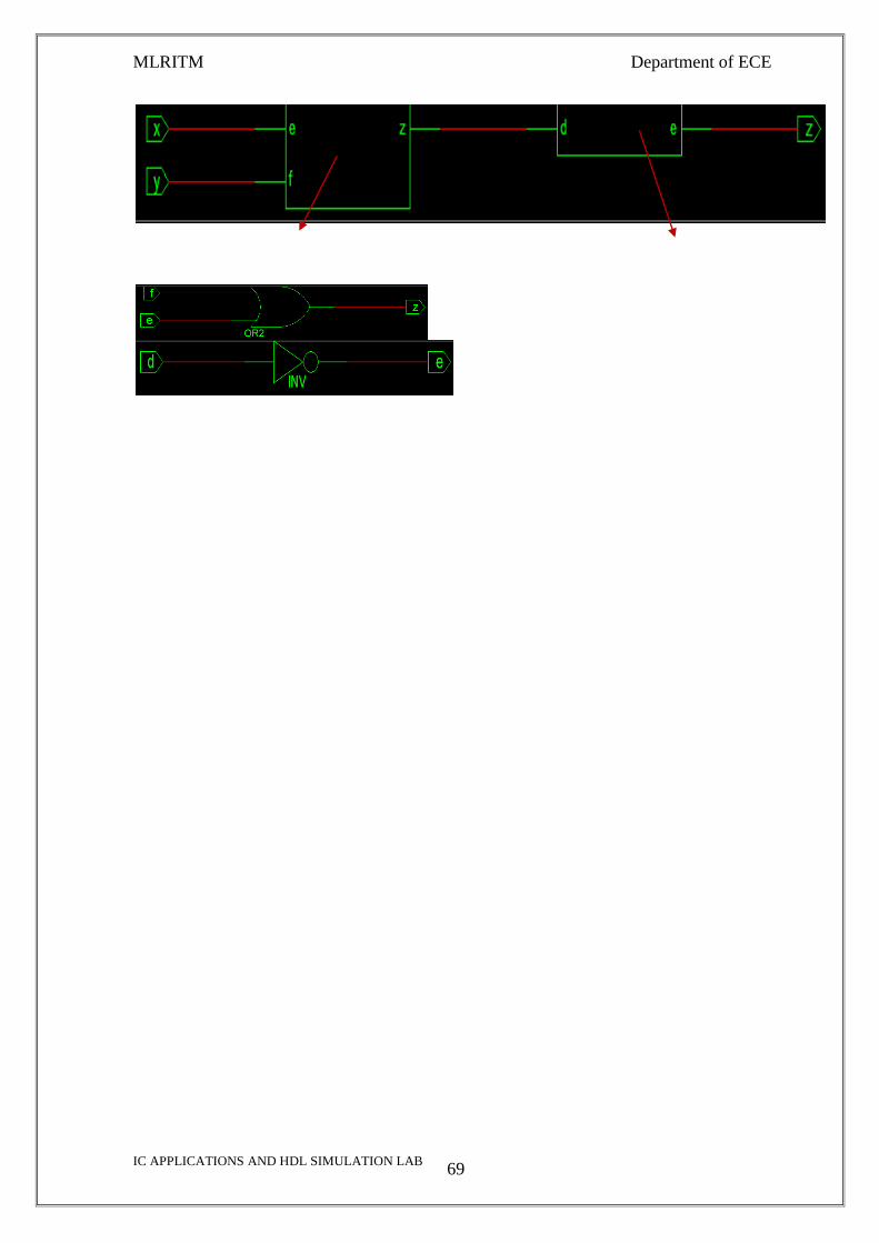
Block Diagram:
MLRITM Department of ECE
IC APPLICATIONS AND HDL SIMULATION LAB
81
Program:
library IEEE;
use IEEE.STD_LOGIC_1164.ALL;
use IEEE.STD_LOGIC_ARITH.ALL;
use IEEE.STD_LOGIC_UNSIGNED.ALL;
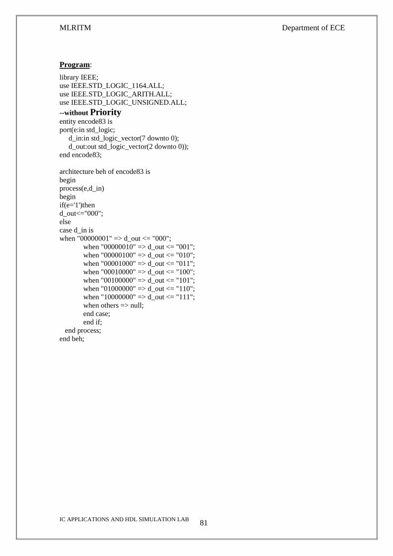
--without Priority
entity encode83 is
port(e:in std_logic;
d_in:in std_logic_vector(7 downto 0);
d_out:out std_logic_vector(2 downto 0));
end encode83;
architecture beh of encode83 is
begin
process(e,d_in)
begin
if(e='1')then
d_out<="000";
else
case d_in is
when "00000001" => d_out <= "000";
when "00000010" => d_out <= "001";
when "00000100" => d_out <= "010";
when "00001000" => d_out <= "011";
when "00010000" => d_out <= "100";
when "00100000" => d_out <= "101";
when "01000000" => d_out <= "110";
when "10000000" => d_out <= "111";
when others => null;
end case;
end if;
end process;
end beh;

MLRITM Department of ECE
IC APPLICATIONS AND HDL SIMULATION LAB
82
Simulation Waveform:
Synthesis Report:
==================================================================
=========
* Final Report *
==================================================================
=========
Cell Usage :
# BELS : 87
# AND2 : 13
# AND3 : 15
# INV : 43
# OR2 : 5
# OR3 : 1
# XOR2 : 10
# FlipFlops/Latches : 3
# LD : 3
# IO Bu ffers : 12
# IBUF : 9
# OBUF : 3
==================================================================
=======

MLRITM Department of ECE
IC APPLICATIONS AND HDL SIMULATION LAB
83
RTL Schematic:

MLRITM Department of ECE
IC APPLICATIONS AND HDL SIMULATION LAB
84
3.2 Design of 8-to-3 Encoder (With Priority)
Aim: To Design and verify the functionality of 8 to 3 priority Encoder.
Apparatus:
Personal Computer:1 No
Operating System : Windows XP.
Software : Xilinx 9.2i.
Program:
library IEEE;
use IEEE.STD_LOGIC_1164.ALL;
use IEEE.STD_LOGIC_ARITH.ALL;
use IEEE.STD_LOGIC_UNSIGNED.ALL;
--with priority:
entity encode83wp is
port(e:in std_logic;
d_in:in std_logic_vector(7 downto 0);
d_out:out std_logic_vector(2 downto 0));
end encode83wp;
architecture beh of encode83wp is
begin
process(e,d_in)
begin
if(e='1')then
d_out<="000";
else
case d_in is
when "00000111" => d_out <= "000";
when "00000110" => d_out <= "001";
when "00000101" => d_out <= "010";
when "00000100" => d_out <= "011";
when "00000011" => d_out <= "100";
when "00000010" => d_out <= "101";
when "00000001" => d_out <= "110";
when "00000000" => d_out <= "111";
when others => null;
end case;
end if;
end process;
end beh;

MLRITM Department of ECE
IC APPLICATIONS AND HDL SIMULATION LAB
85
Simulation Waveform:
Result: Designed and verified 8 to 3 priority encoder is by synthesizing and simulating the code.

MLRITM Department of ECE
IC APPLICATIONS AND HDL SIMULATION LAB
86
Viva questions
1. Define encoder ?
2. Define priority encoder ?
3. Difference between encoder and priority encoder ?
4. What are the advantages of encoder ?
5. What are the applications of encoder ?
6. Explain the difference between encoder and decoder ?
7. How many 4 to 2 encoders are required to construct 8 to 3 encoder ?
8. Draw the logic diagram of 4 to 2 encoder ?
9. Draw the logic diagram of 8 to 3 encoder ?
10. What is the IC no of 8 to 3 encoder ?

MLRITM Department of ECE
IC APPLICATIONS AND HDL SIMULATION LAB
87
EXERCISE PROBLEMS
1. To simulate and verify the 4 to 2 encoder (without priority) with dataflow
model.
2. To simulate and verify the 8 to 3 encoder (without priority) with dataflow
model.
3. Write a VHDL code for 4 to 2 encoder (without priority) with behavioral
model.
4. To simulate and verify the decimal to BCD encoder (without priority) with
dataflow model.
5. To simulate and verify the decimal to BCD encoder (without priority) with
behavioral model.
6. To simulate and verify the octal to binary encoder (without priority) with
dataflow model.
7. To simulate and verify the octal to binary encoder (without priority) with
behavioral model.
8. Write a VHDL code for 4 to 2 encoder (with priority) with dataflow model.
9. Write a VHDL code for 4 to 2 encoder (with priority) with behavioral model.
10. 10. To simulate and verify the 8 to 3 encoder (with priority) with dataflow
model.
11. To simulate and verify the 4 to 2 encoder(with priority) with structural model
12. To simulate and verify the 4 to 2 encoder (with out priority) with structural
model
13. To simulate and verify the 8 to 3 encoder (with out priority) with behavioral
model
14. To simulate and verify the 8 to 3 encoder (with out priority) with data flow
model
15. To simulate and verify the 8 to 3 encoder (with out priority) with structural
model.
16. To simulate and verify the 8 to 3 encoder (with priority) with behavioral
model
17. To simulate and verify the 8 to 3 encoder (with priority) with data flow model
18. To simulate and verify the 8 to 3 encoder (with priority) with structural model
19. To simulate and verify the 16 to 4 encoder (with priority) with behavioral
model
20. To simulate and verify the 16 to 4 encoder (without priority) with behavioral
model

MLRITM Department of ECE
IC APPLICATIONS AND HDL SIMULATION LAB
88
4. Design of 8-to-1 Multiplexer
Aim: To simulate and verify the 8 to 1 Multiplexer with Behavioral Model
Apparatus:
Personal Computer:1 No
Operating System : Windows XP,
Software : Xilinx 9.2i.
Program:
library ieee;
use ieee.std_logic_1164.all;
use ieee.std_logic_arith.all;
use ieee.std_logic_unsigned.all;
entity mux_81 is
port (en: in std_logic;
a: in std_logic_vector (2 downto 0);
xin: in std_logic_vector (7 downto 0);
xout1: out std_logic;
xout2: out std_logic);
end mux_81;
architecture behavioral of mux_81 is
begin
process(en, a, xin)
begin
if (en = '0') then
xout1 <= '0'; xout2 <= '1';
else
case a is
when "000" => xout1 <= xin (0); xout2 <= not xin(0);
when "001" => xout1 <= xin (1); xout2 <= not xin(1);
when "010" => xout1 <= xin (2); xout2 <= not xin(2);
when "011" => xout1 <= xin (3); xout2 <= not xin(3);
when "100" => xout1 <= xin (4); xout2 <= not xin(4);
when "101" => xout1 <= xin (5); xout2 <= not xin(5);
when "110" => xout1 <= xin (6); xout2 <= not xin(6);
when "111" => xout1 <= xin (7); xout2 <= not xin(7);
when others => null;
end case;
end if;
end process;
end behavioral;

MLRITM Department of ECE
IC APPLICATIONS AND HDL SIMULATION LAB
89
Simulation Waveform:
Synthesis Report:
==================================================================
=========
* Final Report *
==================================================================
=========
Cell Usage :
# BELS : 47
# AND2 : 18
# INV : 15
# OR2 : 14
# IO Buffers : 14
# IBUF : 12
# OBUF : 2
==================================================================
=========

MLRITM Department of ECE
IC APPLICATIONS AND HDL SIMULATION LAB
90
RTL Schematic:
Result: Designed and Verified 8 to 1 Multiplexer.

MLRITM Department of ECE
IC APPLICATIONS AND HDL SIMULATION LAB
91
Viva questions
1. Define multiplexer ?
2. Define demultiplexer ?
3. Explain the difference between multiplexer and demultiplexer ?
4. Explain the applications of multiplexers ?
5. Explain the applications of demultiplexers ?
6. How many 4: 1 multiplexers are required to design one 8:1 multiplexer ?
7. What is the use of selection lines in MUX?
8. what are the other names of multiplexers ?
9. What is the difference between MUX and decoder ?
10. why multiplexer is called as data selector ?
EXERCISE PROBLEMS
1. To simulate and verify the 4 to 1 MUX with dataflow model.
2. To simulate and verify the 4 to 1 MUX with behavioral model.
3. To simulate and verify the 8 to 1 MUX with dataflow model.
4. To simulate and verify the 8 to 1 MUX with behavioral model.
5. To simulate and verify the 16 to 1 MUX with dataflow model.
6. To simulate and verify the 16 to 1 MUX with behavioral model.
7. To simulate and verify the 4 to 1 MUX with structural model.
8. To simulate and verify the 8 to 1 MUX with structural model.
9. To simulate and verify the 2 to 1 MUX with structural model
10. To simulate and verify the 2 to 1 MUX with behavioral model
11. To simulate and verify the 2 to 1 MUX with data flow model
12. To simulate and verify the 16 to 1 MUX with structural model
13. To simulate and verify the 32 to 1 MUX with data flow model
14. To simulate and verify the 32 to 1 MUX with behavioral model
15. To simulate and verify the 32 to 1 MUX with Structural model
16. To simulate and verify the 64 to 1 MUX with data flow model
17. To simulate and verify the 64 to 1 MUX with behavioral model
18. To simulate and verify the 64 to 1 MUX with Structural model

MLRITM Department of ECE
IC APPLICATIONS AND HDL SIMULATION LAB
92
5. Design of 4 bit binary to gray converter
Aim: To simulate and verify the 4 bit binary to gray converter
Apparatus:
Personal Computer:1 No
Operating System : Windows XP,
Software : Xilinx 9.2i.
Program:
library IEEE;
use IEEE.STD_LOGIC_1164.ALL;
use IEEE.STD_LOGIC_ARITH.ALL;
use IEEE.STD_LOGIC_UNSIGNED.ALL;
entity bi_to_g is
port(b:in std_logic_vector(3 downto 0);
g:out std_logic_vector(3 downto 0));
end bi_to_g;
architecture df of bi_to_g is
begin
g(3)<=b(3);
g(2)<=b(3) xor b(2);
g(1)<=b(2) xor b(1);
g(0)<=b(1) xor b(0);
end df;

MLRITM Department of ECE
IC APPLICATIONS AND HDL SIMULATION LAB
93
Simulation Waveform:
Synthesis Report:
==================================================================
=========
* Final Report *
==================================================================
=========
Cell Usage :
# BELS : 3
# XOR2 : 3
# IO Buffers : 8
# IBUF : 4
# OBUF : 4
==================================================================
=========
RTL Schematic:

MLRITM Department of ECE
IC APPLICATIONS AND HDL SIMULATION LAB
94
Viva questions
1. What is the difference between binary and BCD code ?
2. Convert 1010 into gray code ?
3. Convert the gray code 1010011 into binary code ?
4. Convert 101010 binary code into bcd code ?
5. Convert 10100101 bcd code into binary code ?
6. Convert 8547.A5D into decimal code?
7. Convert 58A.52 into octal code?
8. Convert 854.124 into hexa decimal code?
9. Define ASCII.
10. Define EBCDIC.

MLRITM Department of ECE
IC APPLICATIONS AND HDL SIMULATION LAB
95
EXERCISE PROBLEMS
1. To simulate and verify the 4-bit gray to binary code converter.
2. To simulate and verify the 3-bit binary to BCD code converter.
3. To simulate and verify the 3-bit binary to gray code converter.
4. To simulate and verify the 4-bit gray to binary code converter.
5. To simulate and verify the 4-bit BCD to binary code converter using data flow
model
6. To simulate and verify the 4-bit BCD to binary code converter using
behavioural model
7. To simulate and verify the 3-bit BCD to Excess-3 code converter using
behavioural model
8. To simulate and verify the 3-bit BCD to Excess-3 code converter using data
flow model
9. To simulate and verify the 3-bit Excess-3 to BCD code converter using
behavioural model
10. To simulate and verify the 3-bit Excess-3 to BCD code converter using data
flow model
11. To simulate and verify the 3-bit binary to Excess-3 code converter
12. To simulate and verify the 4-bit binary to Excess-3 code converter
13. To simulate and verify the 3-bit BCD to Excess-3 code converter
14. To simulate and verify the 4-bit BCD to Excess-3 code converter
15. To simulate and verify the 3-bit Gray code to Excess-3 code converter
16. To simulate and verify the 3-bit Gray code to BCD code converter
17. To simulate and verify the 4-bit Gray code to Excess-3 code converter
18. To simulate and verify the 4-bit Gray code to BCD code converter
19. To simulate and verify the 2-bit Gray code to Excess-3 code converter
20. To simulate and verify the 2-bit Gray code to BCD code converter

MLRITM Department of ECE
IC APPLICATIONS AND HDL SIMULATION LAB
96
6 Design of 4 bit Comparator
Aim: To simulate and verify the Comparator.
Apparatus:
Personal Computer:1 No
Operating System : Windows XP,
Software : Xilinx 9.2i.
Program:
library IEEE;
use IEEE.STD_LOGIC_1164.ALL;
use IEEE.STD_LOGIC_ARITH.ALL;
use IEEE.STD_LOGIC_UNSIGNED.ALL;
entity comparator4 is
Port ( a,b : in STD_LOGIC_vector(3 downto 0);
x,y,z: out STD_LOGIC
);
end comparator4;
architecture Behavioral of comparator4 is
begin
process(a,b)
begin
if (a>b) then x<='1';else x<='0';
end if;
if (a<b) then y<='1'; else y<='0';
end if;
if (a=b) then z<='1'; else z<='0';
end if;
end process;
end Behavioral;

MLRITM Department of ECE
IC APPLICATIONS AND HDL SIMULATION LAB
97
Simulation Waveform:
Synthesis Report:
==================================================================
=========
* Final Report *
==================================================================
=========
Cell Usage :
# BELS : 51
# AND2 : 8
# AND3 : 4
# AND4 : 1
# INV : 20
# OR2 : 14
# XOR2 : 4
# IO Buffers : 11
# IBUF : 8
# OBUF : 3 ==================================================================
=========
RTL Schematic:

MLRITM Department of ECE
IC APPLICATIONS AND HDL SIMULATION LAB
98
Viva Questions
1. Which IC is used as magnitude comparator?
2. What is the drawback of comparator?
3. What is false triggering?
4. What is zero crossing detector?
5. What are the applications of comparator?
6. What are applications of Schmitt trigger?
7. Define UTP.
8. Define LTP.
9. What is hysteresis?
10. What is the other name of Hysteresis?
EXERCISE PROBLEMS
1. To simulate and verify the 1 to 4 DEMUX with behavioral model.
2. To simulate and verify the 1 to 4 DEMUX with dataflow model.
3. To simulate and verify the 1 to 8 DEMUX with behavioral model.
4. To simulate and verify the 1 to 8 DEMUX with dataflow model.
5. Implement full subtractor using 1 to 8 DEMUX and verify it.
6. Implement full subtractor using 1 to 4 DEMUX and verify it.
7. To simulate and verify the 2-bit comparator with behavioral model.
8. To simulate and verify the 1 to 2 DEMUX with behavioral model
9. To simulate and verify the 1 to 2 DEMUX with data flow model
10. To simulate and verify the 1 to 2 DEMUX with structural model
11. To simulate and verify the 1 to 4 DEMUX with behavioral model
12. To simulate and verify the 1 to 4 DEMUX with data flow model
13. To simulate and verify the 1 to 4 DEMUX with structural model
14. To simulate and verify the 1 to 8 DEMUX with behavioral model
15. To simulate and verify the 1 to 8 DEMUX with data flow model
16. To simulate and verify the 1 to 8 DEMUX with structural model
17. Implement Half-Subtractor using 1 to 8 DEMUX and verify
18. Implement Half-Subtractor using 1 to 4 DEMUX and verify
19. To simulate and verify 2 bit comparator with data flow model
20. To simulate and verify 3 bit comparator with data flow model
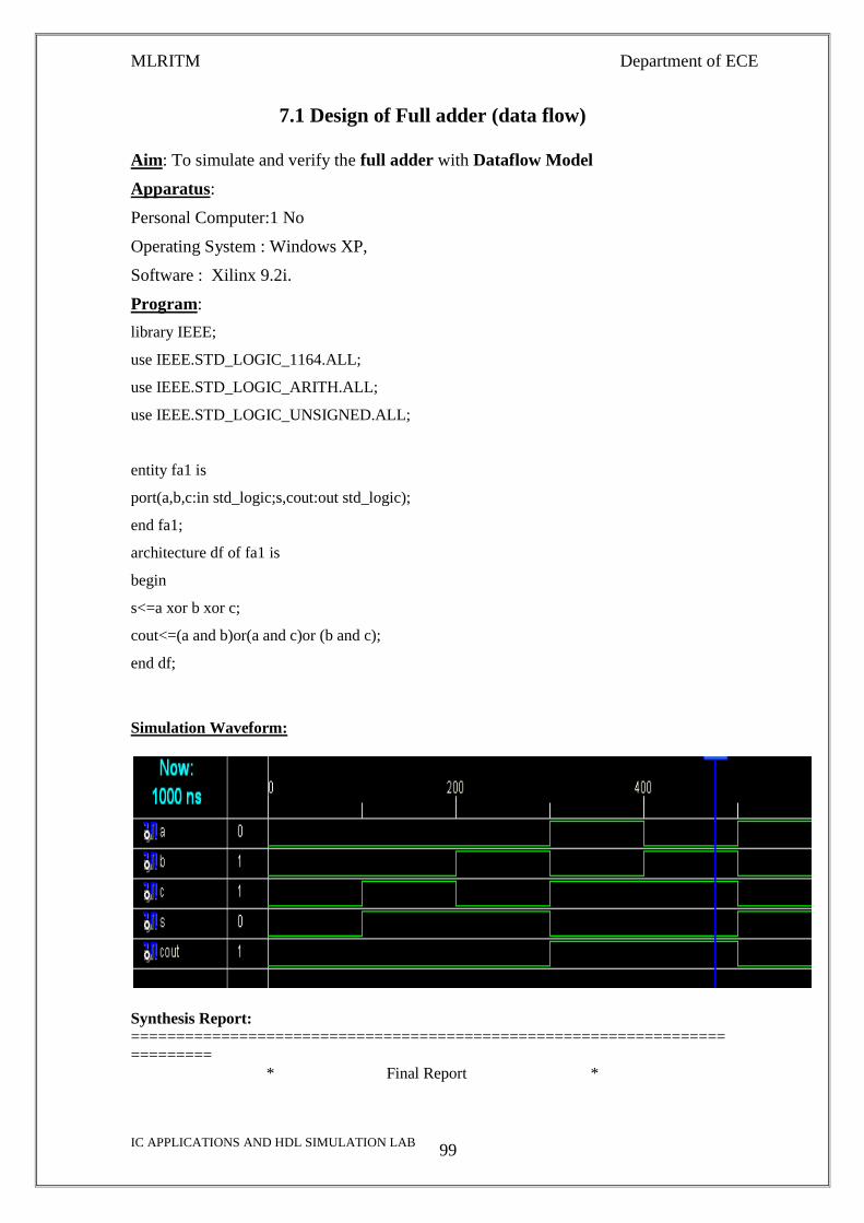
MLRITM Department of ECE
IC APPLICATIONS AND HDL SIMULATION LAB
99
7.1 Design of Full adder (data flow)
Aim: To simulate and verify the full adder with Dataflow Model
Apparatus:
Personal Computer:1 No
Operating System : Windows XP,
Software : Xilinx 9.2i.
Program:
library IEEE;
use IEEE.STD_LOGIC_1164.ALL;
use IEEE.STD_LOGIC_ARITH.ALL;
use IEEE.STD_LOGIC_UNSIGNED.ALL;
entity fa1 is
port(a,b,c:in std_logic;s,cout:out std_logic);
end fa1;
architecture df of fa1 is
begin
s<=a xor b xor c;
cout<=(a and b)or(a and c)or (b and c);
end df;
Simulation Waveform:
Synthesis Report:
==================================================================
=========
* Final Report *
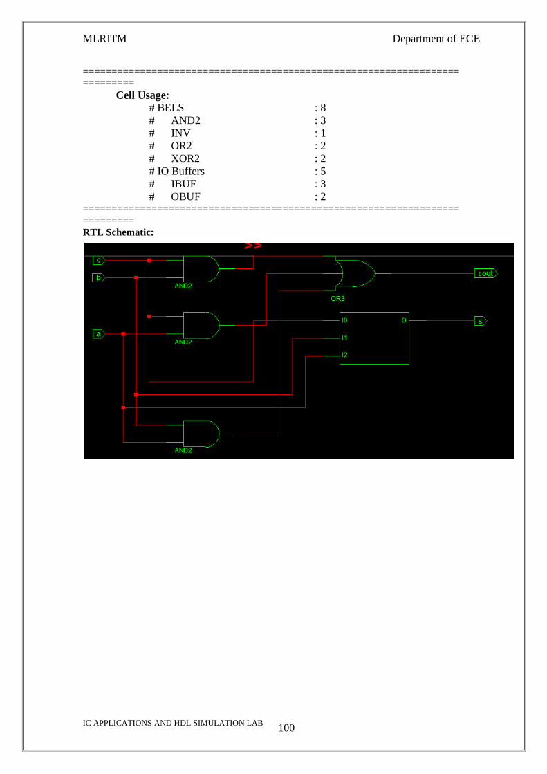
MLRITM Department of ECE
IC APPLICATIONS AND HDL SIMULATION LAB
100
==================================================================
=========
Cell Usage:
# BELS : 8
# AND2 : 3
# INV : 1
# OR2 : 2
# XOR2 : 2
# IO Buffers : 5
# IBUF : 3
# OBUF : 2 ==================================================================
=========
RTL Schematic:

MLRITM Department of ECE
IC APPLICATIONS AND HDL SIMULATION LAB
101
7.2 Design of Full adder (Behavioral Model)
Aim: To simulate and verify the full adder with Behavioral Model
Apparatus:
Personal Computer:1 No
Operating System : Windows XP,
Software : Xilinx 9.2i.
Program:
library IEEE;
use IEEE.STD_LOGIC_1164.ALL;
use IEEE.STD_LOGIC_ARITH.ALL;
use IEEE.STD_LOGIC_UNSIGNED.ALL;
entity fulladder1 is
port(a:in std_logic_vector(2 downto 0);
s,ca:out std_logic);
end fulladder1;
architecture behavioral of fulladder1 is
begin
process(a)
begin
if a="000" then s<='0';ca<='0';
elsif a="001" then s<='1';ca<='0';
elsif a="010" then s<='1';ca<='0';
elsif a="011" then s<='0';ca<='1';
elsif a="100" then s<='1';ca<='0';
elsif a="101" then s<='0';ca<='1';
elsif a="110" then s<='0';ca<='1';
else s<='1';ca<='1';
end if;
end process;
end behavioral;

MLRITM Department of ECE
IC APPLICATIONS AND HDL SIMULATION LAB
102
Simulation Waveform:
Synthesis Report:
==================================================================
=========
* Final Report *
==================================================================
=========
Cell Usage:
# BELS : 19
# AND2 : 8
# INV : 6
# OR2 : 5
# IO Buffers : 5
# IBUF : 3
# OBUF : 2 ==================================================================
=========
RTL Schematic:

MLRITM Department of ECE
IC APPLICATIONS AND HDL SIMULATION LAB
103
7.3 Design of Full adder (with select)
Aim: To simulate and verify the full adder with ‘with select’
Apparatus:
Personal Computer:1 No
Operating System : Windows XP,
Software : Xilinx 9.2i.
Program:
library IEEE;
use IEEE.STD_LOGIC_1164.ALL;
use IEEE.STD_LOGIC_ARITH.ALL;
use IEEE.STD_LOGIC_UNSIGNED.ALL;
entity fa_select is
port(a:in bit_vector(2 downto 0);
s:out bit_vector(1 downto 0));
end fa_select ;
architecture df of fa_select is
begin
with a select
s<=("00")when"000",
("10")when"001",
("10")when"010",
("01")when"011",
("10")when"100",
("01")when"101",
("01")when"110",
("11")when"111";
end df;

MLRITM Department of ECE
IC APPLICATIONS AND HDL SIMULATION LAB
104
Simulation Waveform:
Synthesis Report:
==================================================================
=========
* Final Report *
==================================================================
=========
Cell Usage:
# BELS : 19
# AND2 : 8
# INV : 6
# OR2 : 5
# IO Buffers : 5
# IBUF : 3
# OBUF : 2 ==================================================================
=========

MLRITM Department of ECE
IC APPLICATIONS AND HDL SIMULATION LAB
105
RTL Schematic:

MLRITM Department of ECE
IC APPLICATIONS AND HDL SIMULATION LAB
106
7.4 Design of Full adder (Structural Model)
Aim: To simulate and verify the full adder with Dataflow Model
Apparatus:
Personal Computer:1 No
Operating System : Windows XP,
Software : Xilinx 9.2i.
Program:
library IEEE;
use IEEE.STD_LOGIC_1164.ALL;
use IEEE.STD_LOGIC_ARITH.ALL;
use IEEE.STD_LOGIC_UNSIGNED.ALL;
entity fa2 is
port(a1,b1,c1:in std_logic;sum,cout1:out std_logic);
end fa2;
architecture struc of fa2 is
component xor12 is
port(p,q:in std_logic; x:out std_logic);
end component;
component and12 is
port(c,d:in std_logic;y:out std_logic);
end component;
component or12 is
port(e,f:in std_logic;z:out std_logic);
end component;
signal s1,s2,s3,s4,s5:std_logic;
begin
d1:xor12 port map(a1,b1,s1);
d2:xor12 port map(s1,c1,sum);
d3:and12 port map(a1,b1,s2);
d4:and12 port map(a1,c1,s3);
d5:and12 port map(b1,c1,s4);
d6:or12 port map(s2,s3,s5);
d7:or12 port map(s4,s5,cout1);
end struc;

MLRITM Department of ECE
IC APPLICATIONS AND HDL SIMULATION LAB
107
Simulation Waveform:
Synthesis Report:
==================================================================
=========
* Final Report *
==================================================================
=========
Cell Usage:
# BELS : 6
# AND2 : 2
# OR2 : 2
# XOR2 : 2
# IO Buffers : 5
# IBUF : 3
# OBUF : 2 ==================================================================
=========
RTL Schematic:

MLRITM Department of ECE
IC APPLICATIONS AND HDL SIMULATION LAB
108
Viva Questions
1. What is the sum expression of full adder?
2. What is the carry expression of full adder?
3. What is the difference expression of full subtractor?
4. What is the borrow expression of full subtractor?
5. How many half adders are required to construct full adder?
6. How many half subtractors are required to construct full subtractor?
7. To implement 4 bit parallel adder how many full adders are required?
8. To implement 4 bit parallel adder how many full adders and half adders are
required?
9. What is the drawback of serial adder?
10. What is the advantage of carry look ahead adder?
EXERCISE PROBLEMS
1. To simulate and verify the full adder by using two half adders.
2. Design 3-bit full adder of the inputs a=0, b=0, c=1 with dataflow model and
verify it.
3. Design 3-bit full adder of the inputs a=0, b=1, c=0 with dataflow model and
verify it.
4. Design 3-bit full adder of the inputs a=0, b=1, c=1 with dataflow model and
verify it.
5. Design 3-bit full adder of the inputs a=1, b=0, c=0 with dataflow model and
verify it.
6. Design 3-bit full adder of the inputs a=1, b=0, c=1 with dataflow model and
verify it.
7. Design 3-bit full adder of the inputs a=1, b=1, c=0 with behavioral model and
verify it.
8. Design 3-bit full adder of the inputs a=1, b=1, c=1 with behavioral model and
verify it.
9. Design 3-bit full adder of the inputs a=1, b=0, c=1 with behavioral model and
verify it.

MLRITM Department of ECE
IC APPLICATIONS AND HDL SIMULATION LAB
109
10. Design 3-bit full adder of the inputs a=1, b=1, c=0 with dataflow model and
verify it.
11. Design 3 bit full adder with the inputs a=0; b=1; c=0 with behavioral model
and verify
12. Design 3 bit full adder with the inputs a=0; b=1; c=1 with behavioral model
and verify
13. Design 3 bit full adder with the inputs a=0; b=0; c=1 with behavioral model
and verify
14. Design 3 bit full adder with the inputs a=1; b=1; c=0 with behavioral model
and verify
15. Design 3 bit full adder with the inputs a=1; b=0; c=0 with behavioral model
and verify
16. Design 3 bit full adder with the inputs a=1; b=0; c=1 with behavioral model
and verify
17. Design 3 bit full adder with the inputs a=1; b=1; c=1 with behavioral model
and verify
18. Design 3 bit full adder with the inputs a=0; b=1; c=1 with behavioral model
and verify
19. Design 3 bit full adder with the inputs a=1; b=1; c=1 with data flow model and
verify
20. Design 3 bit full adder with the inputs a=0; b=1; c=1 with data flow model
and verify

MLRITM Department of ECE
IC APPLICATIONS AND HDL SIMULATION LAB
110
8.1 Design of SR Flip Flop
Aim: To simulate and verify the SR flip flop with Behavioral model
Apparatus:
Personal Computer:1 No
Operating System : Windows XP,
Software : Xilinx 9.2i.
Program:
library IEEE;
use IEEE.STD_LOGIC_1164.ALL;
use IEEE.STD_LOGIC_ARITH.ALL;
use IEEE.STD_LOGIC_UNSIGNED.ALL;
entity sr_ff is
port(s,r,clk,clr : in std_logic;
q:inout std_logic:=’0’;
qbar : out std_logic);
end sr_ff;
architecture beh of sr_ff is
begin
process(clk)
begin
if(clk'event and clk='1') then
if(clr='1') then
q<='0';qbar<='1';
elsif(clr='0' and s='0' and r='0')then
q<=q;qbar<=not q;
elsif(s='0' and r='1')then
q<='0';qbar<='1';
elsif(s='1' and r='0')then
q<='1';qbar<='0';
else
q<='Z';qbar<='Z';
end if;
end if;
end process;
end beh;

MLRITM Department of ECE
IC APPLICATIONS AND HDL SIMULATION LAB
111
Simulation Waveform:
Synthesis Report:
==================================================================
=========
* Final Report *
==================================================================
=========
Cell Usage:
# BELS : 24
# AND2 : 8
# GND : 1
# INV : 11
# OR2 : 2
# OR3 : 2
# FlipFlops/Latches : 4
# FD : 2
# FDCE : 2
# IO Buffers : 6
# IBUF : 4
# IOBUFE : 1
# OBUFE : 1 ==================================================================
=========
RTL Schematic:
MLRITM Department of ECE
IC APPLICATIONS AND HDL SIMULATION LAB
112
8.2 Design of D Flip Flop
Aim: To simulate and verify the D flip flop with Behavioral model
Apparatus:
Personal Computer:1 No
Operating System : Windows XP,
Software : Xilinx 9.2i.
Program:
library IEEE;
use IEEE.STD_LOGIC_1164.ALL;
use IEEE.STD_LOGIC_ARITH.ALL;
use IEEE.STD_LOGIC_UNSIGNED.ALL;
entity dff is
Port ( d : in STD_LOGIC;
clk : in STD_LOGIC;
clr: in STD_LOGIC;
q : inout STD_LOGIC:=’0’
qbar:out std_logic);
end dff;
architecture Behavioral of dff is
begin
process(clk,clr)
begin
if(clk'event and clk='1') then
if clr='1' then q<='0';
else q<=d; qbar<= not d;
end if;
end if;
end process;
end Behavioral;

MLRITM Department of ECE
IC APPLICATIONS AND HDL SIMULATION LAB
113
Simulation Waveform:
Synthesis Report:
==================================================================
=========
* Final Report *
==================================================================
=========
Cell Usage:
# BELS : 4
# AND2 : 1
# INV : 1
# OR2 : 1
# FlipFlops/Latches : 2
# FD : 2
# IO Buffers : 5
# IBUF : 3
# OBUF : 2 ==================================================================
=========
RTL Schematic:
MLRITM Department of ECE
IC APPLICATIONS AND HDL SIMULATION LAB
114
8.3 Design of JK Flip Flop
Aim: To simulate and verify the JK flip flop with Behavioral model
Apparatus:
Personal Computer:1 No
Operating System : Windows XP,
Software : Xilinx 9.2i.
Program:
library IEEE;
use IEEE.STD_LOGIC_1164.ALL;
use IEEE.STD_LOGIC_ARITH.ALL;
use IEEE.STD_LOGIC_UNSIGNED.ALL;
entity jkff is
Port ( jk : in STD_LOGIC_VECTOR(1 downto 0);
Clk,clr : in STD_LOGIC;
q : inout STD_LOGIC:='0');
end jkff;
architecture Behavioral of jkff is
begin
process(clk,jk)
begin
if(clk'event and clk='1') then
if(clr='1')then q<='0';
else
case jk is
when "00"=>q<=q;
when "01"=>q<='0';
when "10"=>q<='1';
when "11"=>q<= not q;
when others=>null;
end case;
end if;
end if;
end process;
end Behavioral;

MLRITM Department of ECE
IC APPLICATIONS AND HDL SIMULATION LAB
115
Simulation Waveform:
Synthesis Report:
==================================================================
=========
* Final Report *
==================================================================
=========
Cell Usage:
# BELS : 8
# AND2 : 3
# INV : 3
# OR2 : 1
# VCC : 1
# FlipFlops/Latches : 1
# FD : 1
# IO Buffers : 6
# IBUF : 4
# OBUF : 2
==================================================================
=========
RTL Schematic:

MLRITM Department of ECE
IC APPLICATIONS AND HDL SIMULATION LAB
116
8.4 Design of T Flip Flop
Aim: To simulate and verify the T flip flop with Behavioral model
Apparatus:
Personal Computer:1 No
Operating System : Windows XP,
Software : Xilinx 9.2i.
Program:
library IEEE;
use IEEE.STD_LOGIC_1164.ALL;
use IEEE.STD_LOGIC_ARITH.ALL;
use IEEE.STD_LOGIC_UNSIGNED.ALL;
entity tff is
Port ( t : in STD_LOGIC;
clk,clr : in STD_LOGIC;
q : inout STD_LOGIC:='0'
qbar: out STD-LOGIC);
end tff;
architecture Behavioral of tff is
begin
process(clk,t)
begin
if(clk'event and clk='1') then
if(clr=’1’)then q<=’0’;qbar<=’1’;
elsif(t='0')then q<=q;qbar<=not q;
else q<=not q;qbar<=q;
end if;
end if;
end process;
end Behavioral;

MLRITM Department of ECE
IC APPLICATIONS AND HDL SIMULATION LAB
117
Simulation Waveform:
Synthesis Report:
==================================================================
=========
* Final Report *
==================================================================
=========
Cell Usage:
# BELS : 11
# AND2 : 3
# GND : 1
# INV : 4
# OR2 :3
# FlipFlops/Latches : 2
# FD :1
# FDCE : 1
# IO Buffers : 5
# IBUF : 3
# OBUF : 2
==================================================================
=========
RTL Schematic:

MLRITM Department of ECE
IC APPLICATIONS AND HDL SIMULATION LAB
118
Review Questions
1. Define Flip-flop.
2. What is the difference between flip-flop and latch?
3. What is the difference between flip-flop and Register?
4. Define ripple counter.
5. What is the drawback of RS flip flop?
6. What is race around condition?
7. What are the applications of D flip flop?
8. Which flip-flop has XOR logic?
9. Which flip-flop has XNOR logic?
10. Write the characteristic equation of T flip flop.
EXERCISE PROBLEMS
1. To simulate and verify the SR flip-flop with data flow model
2. To simulate and verify the SR flip-flop with behavioral model
3. To simulate and verify the SR flip-flop with structural model
4. To simulate and verify the D flip-flop with data flow model
5. To simulate and verify the D flip-flop with behavioral model
6. To simulate and verify the D flip-flop with structural model
7. To simulate and verify the JK flip-flop with data flow model
8. To simulate and verify the JK flip-flop with behavioral model
9. To simulate and verify the JK flip-flop with structural model
10. To simulate and verify the T flip-flop with data flow model
11. To simulate and verify the T flip-flop with behavioral model
12. To simulate and verify the T flip-flop with structural model
13. To simulate and verify the Master Slave JK flip-flop with data flow model
14. To simulate and verify the Master Slave JK flip-flop with behavioral model
15. To simulate and verify the Master Slave JK flip-flop with structural model
16. To simulate and verify D Latch with data flow model
17. To simulate and verify D Latch with behavioral model

MLRITM Department of ECE
IC APPLICATIONS AND HDL SIMULATION LAB
119
9.1 Design of 4-bit binary counter (synchronous)
Aim: To simulate and verify the 4-bit binary counter (synchronous)
Apparatus:
Personal Computer:1 No
Operating System : Windows XP,
Software : Xilinx 9.2i.
Program:
library IEEE;
use IEEE.STD_LOGIC_1164.ALL;
use IEEE.STD_LOGIC_ARITH.ALL;
use IEEE.STD_LOGIC_UNSIGNED.ALL;
entity synbicount is
port (clk: in std_logic;
rst: in std_logic;
q: inout std_logic_vector (3 downto 0));
end synbicount;
architecture behavioral of synbicount is
signal count:std_logic_vector(3 downto 0);
begin
process (clk, rst)
begin
if (clk'event and clk = '1') then
if (rst = '1') then count <= "0000"; --for down counter count=>"1111"
else count <= count + 1; -- for down counter count<=count-1;
end if;
q<= count;
end if;
end process;
end behavioral;

MLRITM Department of ECE
IC APPLICATIONS AND HDL SIMULATION LAB
120
Simulation Waveform:
Synthesis Report:
==================================================================
=========
* Final Report *
==================================================================
=========
Cell Usage:
# BELS : 14
# AND2 : 6
# INV : 5
# XOR2 :3
# FlipFlops/Latches : 8
# FD : 8
# IO Buffers : 6
# IBUF : 2
# OBUF : 4
==================================================================
=========
RTL Schematic:

MLRITM Department of ECE
IC APPLICATIONS AND HDL SIMULATION LAB
121
9.2 Design of 4-bit binary counter (asynchronous)
Aim: To simulate and verify the 4-bit binary counter (asynchronous)
Apparatus:
Personal Computer:1 No
Operating System : Windows XP
Software : Xilinx 9.2i.
Program:
library IEEE;
use IEEE.STD_LOGIC_1164.ALL;
use IEEE.STD_LOGIC_ARITH.ALL;
use IEEE.STD_LOGIC_UNSIGNED.ALL;
entity asybin1 is
port (clk: in std_logic;
rst: in std_logic;
q: inout std_logic_vector (3 downto 0));
end asybin1;
architecture behavioral of asybin1 is
signal count:std_logic_vector(3 downto 0);
begin
process (clk)
begin
if (rst = '1') then count <= "0000"; --for down counter count<="1111"
else if (clk'event and clk = '1') then
count <= count + 1; -- for down counter count<=count-1;
q<= count;
end if;
end if;
end process;
end behavioral;

MLRITM Department of ECE
IC APPLICATIONS AND HDL SIMULATION LAB
122
Simulation Waveform:
Synthesis Report:
==================================================================
=========
* Final Report *
==================================================================
=========
Cell Usage:
# BELS : 8
# AND2 : 2
# GND : 1
# INV : 2
# XOR2 : 3
# FlipFlops/Latches : 8
# FDC : 8
# FDCE : 4
# IO Buffers : 6
# IBUF : 2
# OBUF : 4
==================================================================
=========
RTL Schematic:

MLRITM Department of ECE
IC APPLICATIONS AND HDL SIMULATION LAB
123
9.3 Design of BCD up counter
Aim: To simulate and verify the BCD up counter
Apparatus:
Personal Computer:1 No
Operating System : Windows XP,
Software : Xilinx 9.2i.
Program:
library IEEE;
use IEEE.STD_LOGIC_1164.ALL;
use IEEE.STD_LOGIC_ARITH.ALL;
use IEEE.STD_LOGIC_UNSIGNED.ALL;
entity bcdupcount is
port (clk: in std_logic;
rst: in std_logic;
q: inout std_logic_vector (3 downto 0));
end bcdupcount;
architecture behavioral of bcdupcount is
signal count:std_logic_vector(3 downto 0);
begin
process (clk)
begin
if rst = '0' or count="1010" then count <= "0000"; --for down counter count<="1111"
else if (clk'event and clk = '1') then
count <= count + 1; -- for down counter count<=count-1;
q<= count;
end if;
end if;
end process;
end behavioral;

MLRITM Department of ECE
IC APPLICATIONS AND HDL SIMULATION LAB
124
Simulation Waveform:
Synthesis Report:
==================================================================
=========
* Final Report *
==================================================================
=========
Cell Usage:
# BELS : 15
# AND2 : 5
# GND : 1
# INV : 5
# OR2 : 1
# XOR2 : 3
# FlipFlops/Latches : 8
# FDC : 4
# FDCE : 4
# IO Buffers : 6
# IBUF : 2
# OBUF : 4
==================================================================
=========
RTL Schematic:

MLRITM Department of ECE
IC APPLICATIONS AND HDL SIMULATION LAB
125
9.4 Design of BCD down counter
Aim: To simulate and verify the BCD down counter
Apparatus:
Personal Computer:1 No
Operating System : Windows XP,
Software : Xilinx 9.2i.
Program:
library IEEE;
use IEEE.STD_LOGIC_1164.ALL;
use IEEE.STD_LOGIC_ARITH.ALL;
use IEEE.STD_LOGIC_UNSIGNED.ALL;
entity bcddntcount is
port (clk: in std_logic;
rst: in std_logic;
q: inout std_logic_vector (3 downto 0));
end bcddntcount;
architecture behavioral of bcddntcount is
signal count:std_logic_vector(3 downto 0);
begin
process (clk)
begin
if rst = '0' or count="1111" then count <= "1001"; --for down counter
count<="1111"
else if (clk'event and clk = '1') then
count <= count - 1; -- for down counter count<=count-1;
q<= count;
end if;
end if;
end process;
end behavioral;

MLRITM Department of ECE
IC APPLICATIONS AND HDL SIMULATION LAB
126
Simulation Waveform:
Synthesis Report:
==================================================================
=========
* Final Report *
==================================================================
=========
Cell Usage:
# BELS : 14
# AND4 : 1
# GND : 1
# INV : 6
# OR2 : 3
# XOR2 : 3
# FlipFlops/Latches : 8
# FDC : 2
# FDCE : 4
# FDP : 2
# IO Buffers : 6
# IBUF : 2
# OBUF : 4
==================================================================
=========
RTL Schematic:

MLRITM Department of ECE
IC APPLICATIONS AND HDL SIMULATION LAB
127
Viva Questions
1. Define counter.
2. What is the difference between synchronous counter and asynchronous
counter?
3. What is the difference between counter and register?
4. What is the use of Johnson Counter?
5. What is ring counter?
6. What is the other name of Johnson counter?
7. How many flip-flops are required to design mod-6 counter?
8. How many flip-flops are required to design mod-10 counter?
9. What is the difference between combinational and sequential circuits?
10. Definition of sequential circuits.
EXERCISE PROBLEMS
1. To simulate and verify the 2-bit binary counter (synchronous).
2. To simulate and verify the 3-bit binary counter (synchronous).
3. To simulate and verify the 2-bit binary counter (asynchronous).
4. To simulate and verify the 3-bit binary counter (asynchronous).
5. To simulate and verify the 2-bit BCD up counter.
6. To simulate and verify the 3-bit BCD up counter.
7. To simulate and verify the 2-bit BCD down counter.
8. To simulate and verify the 3-bit BCD down counter.
9. To simulate and verify the 2-bit Ring counter.
10. To simulate and verify the 3-bit Ring counter.
11. To simulate and verify the 2-bit Twisted Ring counter.
12. To simulate and verify the 3-bit Twisted Ring counter.
13. To simulate and verify the 4-bit binary counter (synchronous).
14. To simulate and verify the 4-bit binary counter (asynchronous).
15. To simulate and verify the 4-bit BCD up counter
16. To simulate and verify the 4-bit BCD down counter
17. To simulate and verify the 4-bit Ring counter (synchronous).
18. To simulate and verify the 4-bit Ring counter (asynchronous)

MLRITM Department of ECE
IC APPLICATIONS AND HDL SIMULATION LAB
128
10. Finite State Machine Design
Aim: To develop the source code for finite state machine by using HDL and obtain
the simulation and synthesis.
Apparatus:
Personal Computer: 1 No
Operating System : Windows XP,
Software : Xilinx 9.2i.
The output of a Moore finite state machine depends only on the machine's current
state; transitions are not directly dependent upon input.
The use of a Mealy FSM leads often to a reduction of the number of states.
Present State Next State Output
X = 0 X = 1 X = 0 X = 1 S0 S0 S1 0 0
S1 S0 S3 1 0
S2 S0 S2 1 0
S3 S0 S2 1 0
Block Diagram:
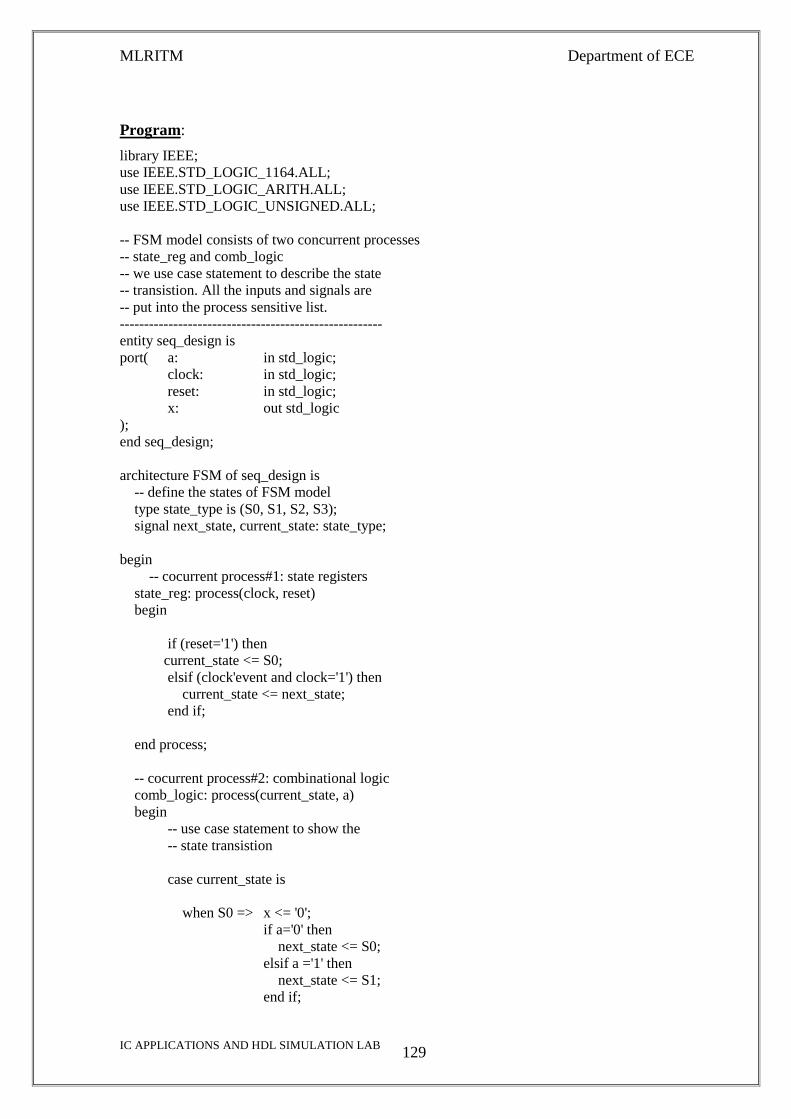
MLRITM Department of ECE
IC APPLICATIONS AND HDL SIMULATION LAB
129
Program:
library IEEE;
use IEEE.STD_LOGIC_1164.ALL;
use IEEE.STD_LOGIC_ARITH.ALL;
use IEEE.STD_LOGIC_UNSIGNED.ALL;
-- FSM model consists of two concurrent processes
-- state_reg and comb_logic
-- we use case statement to describe the state
-- transistion. All the inputs and signals are
-- put into the process sensitive list.
------------------------------------------------------
entity seq_design is
port( a: in std_logic;
clock: in std_logic;
reset: in std_logic;
x: out std_logic
);
end seq_design;
architecture FSM of seq_design is
-- define the states of FSM model
type state_type is (S0, S1, S2, S3);
signal next_state, current_state: state_type;
begin
-- cocurrent process#1: state registers
state_reg: process(clock, reset)
begin
if (reset='1') then
current_state <= S0;
elsif (clock'event and clock='1') then
current_state <= next_state;
end if;
end process;
-- cocurrent process#2: combinational logic
comb_logic: process(current_state, a)
begin
-- use case statement to show the
-- state transistion
case current_state is
when S0 => x <= '0';
if a='0' then
next_state <= S0;
elsif a ='1' then
next_state <= S1;
end if;

MLRITM Department of ECE
IC APPLICATIONS AND HDL SIMULATION LAB
130
when S1 => x <= '0';
if a='0' then
next_state <= S1;
elsif a='1' then
next_state <= S2;
end if;
when S2 => x <= '0';
if a='0' then
next_state <= S2;
elsif a='1' then
next_state <= S3;
end if;
when S3 => x <= '1';
if a='0' then
next_state <= S3;
elsif a='1' then
next_state <= S0;
end if;
when others => x <= '0';
next_state <= S0;
end case;
end process;
end FSM;
Simulation Waveform:
Synthesis Report:
==================================================================
=========
* Final Report *
==================================================================
=========
Cell Usage:
# BELS : 2
# AND2 : 2
# GND : 1
# FlipFlops/Latches : 2
# FTC : 2
# IO Buffers : 4

MLRITM Department of ECE
IC APPLICATIONS AND HDL SIMULATION LAB
131
# IBUF : 3
# OBUF : 1
==================================================================
=========
RTL Schematic:
Result: Thus the program fory FSM has been verified and also simulation
and synthesis reports have been verified.
Viva Questions
1. What is the function of Mealy machine?
2. What is the difference between blocking and non blocking statement?
3. What is the difference between ‘always’ and ’initial’ statements?
4. What is the difference between ‘case x’ and ‘case z’?
5. What is the function of Moore machine?
6. What are the differences between Moore and Mealy machine?
7. What is meant by simulation?
8. What is meant by synthesis?
9. What are advantages of verilog over high level languages?
10. Define Noise margin.

MLRITM Department of ECE
IC APPLICATIONS AND HDL SIMULATION LAB
132
EXERCISE PROBLEMS
1. To simulate and verify the 4-bit binary counter FSM.
2. To simulate and verify the 4-bit BCD down counter FSM.
3. To simulate and verify the 4-bit BCD up counter FSM.
4. To simulate and verify the 4-bit synchronous counter FSM.
5. To simulate and verify the 4-bit asynchronous counter FSM.
6. To simulate and verify 3-bit binary counter FSM
7. To simulate and verify 3-bit BCD down counter FSM
8. To simulate and verify 3-bit BCD up counter FSM
9. To simulate and verify 3-bit synchronous counter FSM
10. To simulate and verify 3-bit asynchronous counter FSM
11. To simulate and verify 4-bit Ring counter FSM
12. To simulate and verify 3-bit Ring counter FSM
13. To simulate and verify 4-bit Twisted Ring counter FSM
14. To simulate and verify 3-bit Twisted Ring counter FSM
15. To simulate and verify the 4-bit binary counter FSM.(Synchronous)
16. To simulate and verify the 4-bit binary counter FSM. .(Asynchronous)
17. To simulate and verify the 3-bit binary counter FSM.(Synchronous)
18. To simulate and verify the 3-bit binary counter FSM. .(Asynchronous)
19. To simulate and verify the 4-bit ring counter FSM.(Synchronous)
20. To simulate and verify the 4-bit ring counter FSM. .(Asynchronous)