Embed Size (px)
Citation preview
D C / D C C o n v e r t e r
DC/DC Converter Selection GuideVer.9.0
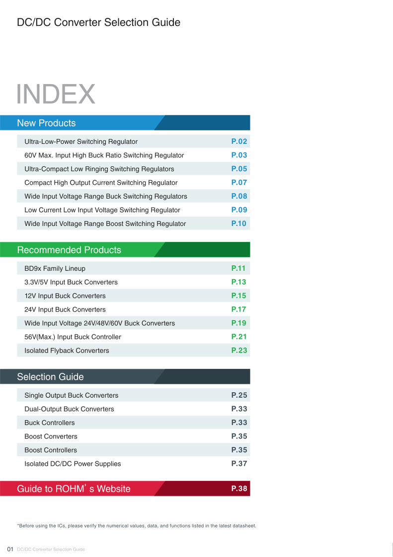
01 DC/DC Converter Selection Guide
DC/DC Converter Selection Guide
New Products
Ultra-Low-Power Switching Regulator P.02
60V Max. Input High Buck Ratio Switching Regulator P.03
Ultra-Compact Low Ringing Switching Regulators P.05
Compact High Output Current Switching Regulator P.07
Wide Input Voltage Range Buck Switching Regulators P.08
Low Current Low Input Voltage Switching Regulator P.09
Wide Input Voltage Range Boost Switching Regulator P.10
Recommended Products
BD9x Family Lineup P.11
3.3V/5V Input Buck Converters P.13
12V Input Buck Converters P.15
24V Input Buck Converters P.17
Wide Input Voltage 24V/48V/60V Buck Converters P.19
56V(Max.) Input Buck Controller P.21
Isolated Flyback Converters P.23
Selection Guide
Single Output Buck Converters P.25
Dual-Output Buck Converters P.33
Buck Controllers P.33
Boost Converters P.35
Boost Controllers P.35
Isolated DC/DC Power Supplies P.37
INDEX
*Before using the ICs, please verify the numerical values, data, and functions listed in the latest datasheet.
Guide to ROHM’s Website P.38
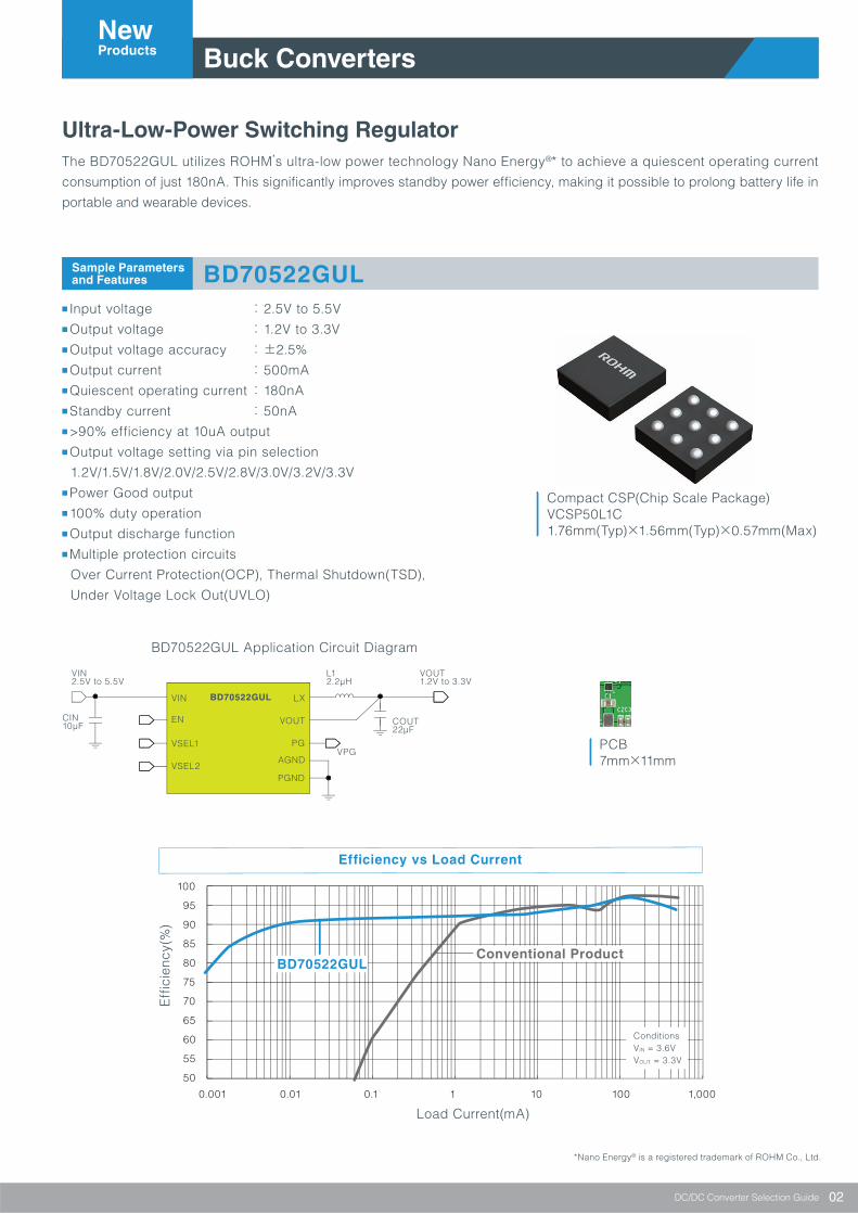
■ Input voltage : 2.5V to 5.5V■ Output voltage : 1.2V to 3.3V■ Output voltage accuracy : ±2.5%■ Output current : 500mA■ Quiescent operating current : 180nA■ Standby current : 50nA■ >90% efficiency at 10uA output■ Output voltage setting via pin selection
1.2V/1.5V/1.8V/2.0V/2.5V/2.8V/3.0V/3.2V/3.3V■ Power Good output■ 100% duty operation■ Output discharge function■ Multiple protection circuits
Over Current Protection(OCP), Thermal Shutdown(TSD),
Under Voltage Lock Out(UVLO)
Buck Converters
DC/DC Converter Selection Guide 02
Ultra-Low-Power Switching Regulator
The BD70522GUL utilizes ROHM’s ultra-low power technology Nano Energy®* to achieve a quiescent operating current
consumption of just 180nA. This significantly improves standby power efficiency, making it possible to prolong battery life in
portable and wearable devices.
NewProducts
BD70522GULSample Parametersand Features
Compact CSP(Chip Scale Package)VCSP50L1C1.76mm(Typ)×1.56mm(Typ)×0.57mm(Max)
Load Current(mA)
0.001
50
55
60
65
70
75
80
85
90
95
100
0.01 0.1 1 10 100 1,000
ConditionsVIN = 3.6VVOUT = 3.3V
Eff
icie
ncy(
%)
PCB7mm×11mm
Efficiency vs Load Current
VIN2.5V to 5.5V
VPG
VOUT1.2V to 3.3V
COUT22µF
L12.2µH
CIN10µF
BD70522GULVIN LX
VOUT
PG
AGND
PGND
EN
VSEL1
VSEL2
BD70522GULConventional Product
BD70522GUL Application Circuit Diagram
*Nano Energy® is a registered trademark of ROHM Co., Ltd.
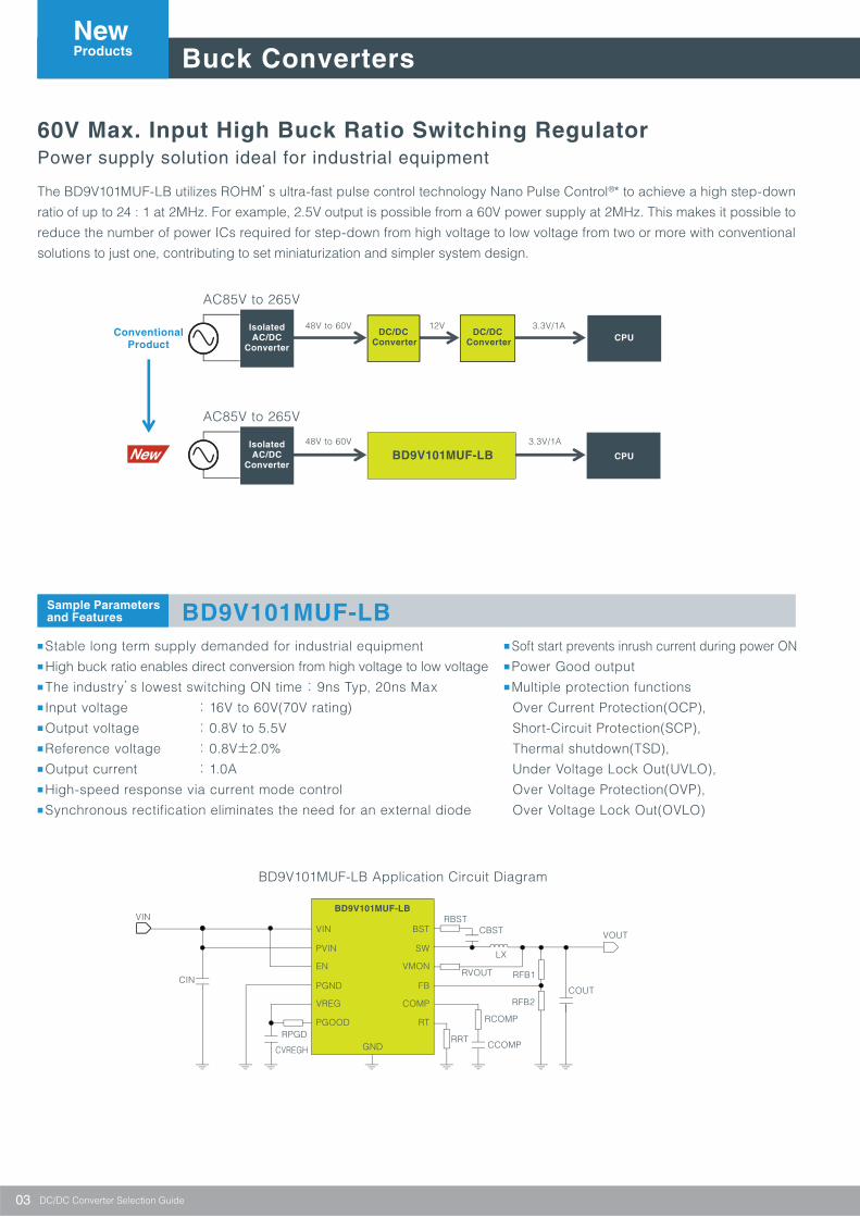
60V Max. Input High Buck Ratio Switching RegulatorPower supply solution ideal for industrial equipment
The BD9V101MUF-LB utilizes ROHM’s ultra-fast pulse control technology Nano Pulse Control®* to achieve a high step-down
ratio of up to 24 : 1 at 2MHz. For example, 2.5V output is possible from a 60V power supply at 2MHz. This makes it possible to
reduce the number of power ICs required for step-down from high voltage to low voltage from two or more with conventional
solutions to just one, contributing to set miniaturization and simpler system design.
BD9V101MUF-LBSample Parametersand Features
03
ConventionalProduct
AC85V to 265V
AC85V to 265V
IsolatedAC/DC
Converter
IsolatedAC/DC
ConverterBD9V101MUF-LB
DC/DCConverter
DC/DCConverter
CPU
CPU
48V to 60V
48V to 60V 3.3V/1A
12V 3.3V/1A
■ Stable long term supply demanded for industrial equipment■ High buck ratio enables direct conversion from high voltage to low voltage■ The industry’s lowest switching ON time : 9ns Typ, 20ns Max■ Input voltage : 16V to 60V(70V rating)■ Output voltage : 0.8V to 5.5V■ Reference voltage : 0.8V±2.0%■ Output current : 1.0A■ High-speed response via current mode control■ Synchronous rectification eliminates the need for an external diode
■ Soft start prevents inrush current during power ON■ Power Good output■ Multiple protection functions
Over Current Protection(OCP),
Short-Circuit Protection(SCP),
Thermal shutdown(TSD),
Under Voltage Lock Out(UVLO),
Over Voltage Protection(OVP),
Over Voltage Lock Out(OVLO)
BD9V101MUF-LB Application Circuit Diagram
VIN
VOUT
COUTCIN
RPGD RRTCVREGH CCOMP
RCOMP
RFB1
CBST
LX
RBST
RVOUT
BD9V101MUF-LB
VIN
PVIN
EN
PGND
VREG
PGOOD
GND
BST
SW
VMON
FB
COMP
RT
RFB2
DC/DC Converter Selection Guide
Buck ConvertersNewProducts
Increasing the switching frequency to 2MHz reduces the size of external components (coil), decreasing mounting area. Further
space savings can be achieved by switching from a 2-stage buck configuration to single stage conversion. Also, the 2MHz
switching frequency is guaranteed to not affect the AM radio band (MW).
04
Conventional PCB47mm×25mm=1,175mm2
BD9V101MUF-LB PCB18mm×20mm=360mm2
-69%
Ultra-High-Speed Pulse Control Technology Nano Pulse Control®*
Buck switching DC/DC converters generate an output
voltage by controlling the switching pulse width. This
pulse width is thicker when the step-down ratio of the
input/output voltage is low and thinner when the ratio is
high. As a result, when stepping down from a 60V power
supply to 2.5V, the switching pulse width becomes
extremely thin due to the high buck ratio (24 : 1). For
example, when the switching frequency is 2MHz the
switching cycle is 500ns, so with a step-down ratio of 24:1
the pulse width becomes ultra-narrow at 20.8ns. ROHM’s
Nano Pulse Control®* technology achieves a pulse width
of just 9ns.
Current mode control detects the current flowing through
the coil, but when the pulse width narrows accurate
current detection is prevented due to ringing caused by
the parasitic inductance within the circuit, resulting in
unstable circuit operation. ROHM’s original Nano Pulse
Control®* technology eliminates the effects of ringing by
feeding back the coil current to the IC, making it possible
to stabilize the output voltage even with narrow pulse
widths using current mode control.
VIN=48V/VOUT=1V/fSW=2.2MHz
VIN
20V/div
VOUT
1V/div
9.5ns switching
pulse width
Nano Pulse Example
200ns/div
*Nano Pulse Control® is a registered trademark of ROHM Co., Ltd.
DC/DC Converter Selection Guide
BD9V101MUF-LB 70 1 16 to 60 0.8 to 5.5Tj
-40 to +150Current VQFN24FV40401.9 to 2.3 Recovery Recovery
Functions
Pow
er G
ood
Ext
erna
lS
ynch
roni
zatio
n
Varia
ble
Sof
t Sta
rt
Syn
chro
nous
Rec
tific
atio
n
Ove
r C
urre
ntP
rote
ctio
n
Ther
mal
Shu
tdow
n
Ove
r Vo
ltag
eP
rote
ctio
n
Ligh
t Loa
d Ef
ficie
ncy
RatedInput(V)
OutputCurrent
(A)
InputVoltage
(V)
OutputVoltage
(V)
OperatingTemperature
(C)
ControlMethod Package
SwitchingFrequency
(MHz)Part No.
05
BD9D322QWZ
■Input voltage range : 4.5V to 18V■ Output voltage range : 0.765V to 7.0V■ Reference voltage : 0.765V±1.6%■ Output current : 3A■ Switching frequency : 700kHz■ Built-In switching FET : 80mΩ, 50mΩ ■ Quiescent current : 0.7mA ■ Fast transient response characteristics via fixed
ON time control■ High efficiency Light Load Mode■ Variable Soft Start■ Multiple protection functions
Over Current Protection(OCP),
Thermal Shutdown(TSD), Under Voltage Lock Out(UVLO)
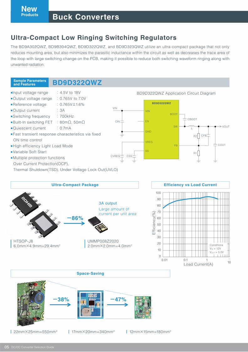
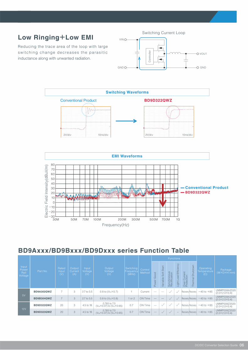
Ultra-Compact Low Ringing Switching Regulators
The BD9A302QWZ, BD9B304QWZ, BD9D322QWZ, and BD9D323QWZ utilize an ultra-compact package that not only
reduces mounting area, but also minimizes the parasitic inductance within the circuit as well as decreases the trace area of
the loop with large switching change on the PCB, making it possible to reduce both switching waveform ringing along with
unwanted radiation.
HTSOP-J86.0mm×4.9mm=29.4mm2
22mm×25mm=550mm2 17mm×20mm=340mm2 12mm×15mm=180mm2
3A output
Large amount ofcurrent per unit area
UMMP008Z20202.0mm×2.0mm=4.0mm2
-86%
-38% -47%
Eff
icie
ncy(
%)
Efficiency vs Load CurrentUltra-Compact Package
Space-Saving
Load Current(A)
ConditionsVIN = 12VVOUT = 5.0V
0.010
10
20
30
40
50
60
70
80
90
100
0.1 110
VIN
CIN
CVREG CSSR1
R2
L
CFB
CBOOT
COUT
VOUT
BD9D322QWZ
VINBOOT
SW
FB
EN
GND
VREG
SS
BD9D322QWZ Application Circuit Diagram
DC/DC Converter Selection Guide
Sample Parametersand Features
Buck ConvertersNewProducts
06
Low Ringing+Low EMI
Reducing the trace area of the loop with large
swi tch ing change decreases the paras i t ic
inductance along with unwanted radiation.
VIN
VOUT
GND GND
Co
ntro
ller
12V
Functions
5VBD9A302QWZ
BD9B304QWZ
BD9D322QWZ
BD9D323QWZ
7
7
20
20
3
3
3
3
1
1 or 2
0.7
0.7
Recovery
Recovery
Recovery
Recovery
Recovery
Recovery
Recovery
Recovery
Current
ON Time
ON Time
ON Time
-40 to +85
-40 to +85
-40 to +85
-40 to +85
2.7 to 5.5
2.7 to 5.5
4.5 to 18
4.5 to 18
0.8 to (VIN×0.7)
0.8 to (VIN×0.8)
0.765 to 7.0(VIN×0.07) to (VIN×0.65)
0.765 to 7.0(VIN×0.07) to (VIN×0.65) -
UMMP008AZ020(2.0×2.0×0.4)
UMMP008AZ020(2.0×2.0×0.4)
UMMP008Z2020(2.0×2.0×0.4)
UMMP008Z2020(2.0×2.0×0.4)
Switching Current Loop
BD9Axxx/BD9Bxxx/BD9Dxxx series Function Table
Switching Waveforms
2V/div 10ns/div2V/dV2VVV/dV ivivvv 10ns010n0ns/div/ddd
BD9D322QWZConventional Product
2V/div 10ns/div 2V/div 10ns/div
EMI Waveforms
Frequency(Hz)
Elec
tric
Fie
ld In
tens
ity(d
BuV
/m) 80
70
60
50
40
30
20
10
0
-10
-20
-3030M 50M 70M 100M 200M 300M 500M 700M 1G
Conventional Product
BD9D322QWZ
DC/DC Converter Selection Guide
OperatingTemperature
(C)Part No.
InputPower
RailVoltage
RatedInput(V)
OutputCurrent
(A)
InputVoltage
(V)
OutputVoltage
(V)
SwitchingFrequency
(MHz)
ControlMethod
Package(W×D×H:mm)
Pow
er G
ood
Varia
ble
Sof
t Sta
rt
Syn
chro
nous
Rec
tific
atio
n
Ove
r C
urre
ntP
rote
ctio
n
Ther
mal
Shu
tdow
n
Ligh
t Loa
d Ef
ficie
ncy
Compact High Output Current Switching Regulator
The BD9F800MUX is a synchronous rectification buck DC/DC converter that integrates a low ON resistance power MOSFET.
A maximum output current of 8A is possible in a compact 3.5mm square package. In addition, fixed ON time control achieves
high-speed load response characteristics and eliminates the need for an external phase compensation circuit.
■ Input voltage : 4.5V to 28V■ Output voltage : 0.765V to 13.5V■ Reference voltage : 0.765V±1.05%■ Output current : 8A■ Switching frequency : 300kHz/600kHz■ Built-In switching FET : 23mΩ, 11mΩ ■ Fast transient response characteristics
via fixed ON time control■ Multiple protection functions
Over Current Protection(OCP),
Short-Circuit Protection(SCP),
Thermal Shutdown(TSD), Under Voltage Lock Out(UVLO)
BD9F800MUX
07
PCB30mm×20mm=600mm2
VQFN11X3535A3.5mm(Typ)×3.5mm(Typ)×0.6mm(Max)
BD9F800MUX Efficiency vs Output Current
VOUT
100mV/div
ILOAD
2A/div
Transient Response Characteristics
500µs/div
Eff
icie
ncy(
%)
Output Current : IOUT(A)
0
10
20
30
40
50
60
70
80
90
100
0 1 2 3 4 5 6 7 8
ConditionsVIN=12VVOUT=3.3VfOSC=300kHz
Ultra-Compact Package
ConditionsVIN=12VVOUT=3.3V
ILOAD=2A→6A→2A
DC/DC Converter Selection Guide
Sample Parametersand Features
Buck ConvertersNewProducts
VIN
VOUT
COUT
R2
R1
CIN
RFREQ
CVREG
Enable
CBOOT
L
BD9F800MUX
VIN
BOOT
SW
VOUT
FB
GND
EN
PGND
FREQ
VREG
PGD
BD9F800MUX Application Circuit Diagram
Eff
icie
ncy(
%)
Output Current : IOUT(A)0 0.5 1.0 1.5 2.0 2.5 3.0 3.5 4.0
0
10
20
30
40
50
60
70
80
90
100
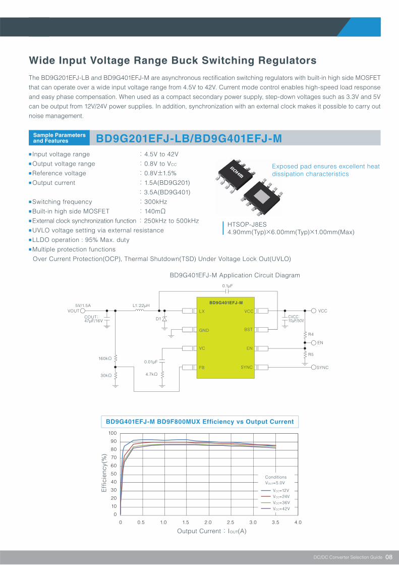
Wide Input Voltage Range Buck Switching Regulators
The BD9G201EFJ-LB and BD9G401EFJ-M are asynchronous rectification switching regulators with built-in high side MOSFET
that can operate over a wide input voltage range from 4.5V to 42V. Current mode control enables high-speed load response
and easy phase compensation. When used as a compact secondary power supply, step-down voltages such as 3.3V and 5V
can be output from 12V/24V power supplies. In addition, synchronization with an external clock makes it possible to carry out
noise management.
■ Input voltage range : 4.5V to 42V■ Output voltage range : 0.8V to VCC
■ Reference voltage : 0.8V±1.5%■ Output current : 1.5A(BD9G201)
: 3.5A(BD9G401)■ Switching frequency : 300kHz■ Built-in high side MOSFET : 140mΩ■ External clock synchronization function : 250kHz to 500kHz■ UVLO voltage setting via external resistance■ LLDO operation : 95% Max. duty■ Multiple protection functions
Over Current Protection(OCP), Thermal Shutdown(TSD) Under Voltage Lock Out(UVLO)
BD9G201EFJ-LB/BD9G401EFJ-M
08
HTSOP-J8ES4.90mm(Typ)×6.00mm(Typ)×1.00mm(Max)
BD9G401EFJ-M BD9F800MUX Efficiency vs Output Current
Exposed pad ensures excellent heatdissipation characteristics
ConditionsVOUT=5.0V
VCC=12VVCC=24VVCC=36VVCC=42V
VOUT VCC
EN
SYNC
5V/1.5A
COUT:47µF/16V
CVCC:10µF/50V
L1:22µH
0.01µF
0.1µF
R4
R5
D1
160kΩ
30kΩ 4.7kΩ
BD9G401EFJ-M
LX VCC
BST
EN
SYNC
GND
VC
FB
BD9G401EFJ-M Application Circuit Diagram
DC/DC Converter Selection Guide
Sample Parametersand Features
Efficiency vs Load Current Battery Life Comparison
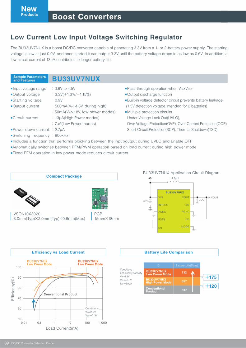
Low Current Low Input Voltage Switching Regulator
■ Input voltage range : 0.6V to 4.5V■ Output voltage : 3.3V(+1.3%/-1.15%)■ Starting voltage : 0.9V■ Output current : 500mA(VIN>1.8V, during high)
: 50mA(VIN>1.8V, low power modes)■ Circuit current : 13µA(High Power modes)
: 7µA(Low Power modes)■ Power down current : 2.7µA■ Switching frequency : 800kHz■ Includes a function that performs blocking between the input/output during UVLO and Enable OFF■Automatically switches between PFM/PWM operation based on load current during high power mode■ Fixed PFM operation in low power mode reduces circuit current
■ Pass-through operation when VIN>VOUT
■ Output discharge function■ Built-in voltage detector circuit prevents battery leakage
(1.5V detection voltage intended for 2 batteries)■ Multiple protection circuits
Under Voltage Lock Out(UVLO),
Over Voltage Protection(OVP), Over Current Protection(OCP),
Short-Circuit Protection(SCP), Thermal Shutdown(TSD)
The BU33UV7NUX is a boost DC/DC converter capable of generating 3.3V from a 1- or 2-battery power supply. The starting
voltage is low at just 0.9V, and once started it can output 3.3V until the battery voltage drops to as low as 0.6V. In addition, a
low circuit current of 13µA contributes to longer battery life.
BU33UV7NUX
09
PCB15mm×18mm
Eff
icie
ncy(
%)
Load Current(mA)
BU33UV7NUX Low Power Mode
BU33UV7NUXLow Power Mode
0.0150
60
70
80
90
100
0.1 1 10 100 1,000
ConditionsVIN=2.5VVOUT=3.3V
Compact Package
VSON10X30203.0mm(Typ)×2.0mm(Typ)×0.6mm(Max)
COUTCINVOUT
BU33UV7NUX Application Circuit Diagram
BU33UV7NUX
VIN VOUT
SW
PGND
FB
MODE
INTLDO
AGND
RSTB
EN
L:4.7µH
Battery Life(Days)IC
712
657
537
BU33UV7NUXLow Power Mode
BU33UV7NUXHigh Power Mode
ConventionalProduct
+175
+120
DC/DC Converter Selection Guide
Sample Parametersand Features
Boost ConvertersNewProducts
Conventional Product
Conditions : 2Ah battery capacityVIN=1.2VVOUT=3.3VIOUT=50µA
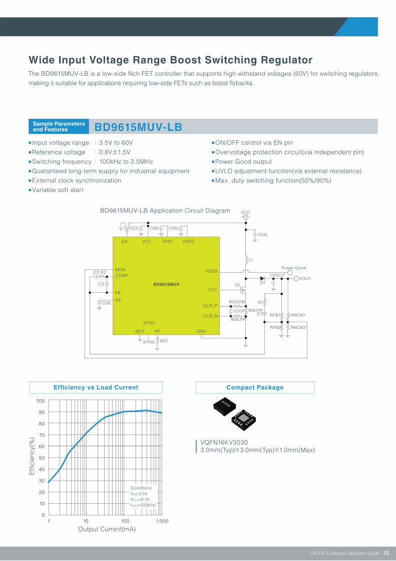
Wide Input Voltage Range Boost Switching Regulator
■ Input voltage range : 3.5V to 60V■ Reference voltage : 0.8V±1.5V■ Switching frequency : 100kHz to 2.5MHz■ Guaranteed long-term supply for industrial equipment■ External clock synchronization■ Variable soft start
■ ON/OFF control via EN pin■ Overvoltage protection circuit(via independent pin)■ Power Good output■ UVLO adjustment function(via external resistance)■ Max. duty switching function(50%/90%)
The BD9615MUV-LB is a low-side Nch FET controller that supports high withstand voltages (60V) for switching regulators,
making it suitable for applications requiring low-side FETs such as boost flybacks.
BD9615MUV-LB
10
BD9615MUV-LB Application Circuit Diagram
VREGVREFVCCEN
MON PGDB
OUT
OCP_P
OCP_M
GND
SYNC
SYNC
MDT RT
COMP
FB
SS
VOUT
VCC
CVREGCVREFCCC
C3
C2
CSS
RRT
ROCPP
RSCPP
ROCPM R1
C1 RFB1 RNCN1
RNCN2RFB2
Q1
CVOUT
Power Good
L1
D1
CVN
COCP
R2
Eff
icie
ncy(
%)
Efficiency vs Load Current Compact Package
Output Current(mA)1
0
10
20
30
40
50
60
70
80
90
100
10 100 1,000
ConditionsVIN=3.5VVOUT=5.1VfOSC=500kHz
VQFN16KV30303.0mm(Typ)×3.0mm(Typ)×1.0mm(Max)
BD9615MUV
DC/DC Converter Selection Guide
Sample Parametersand Features
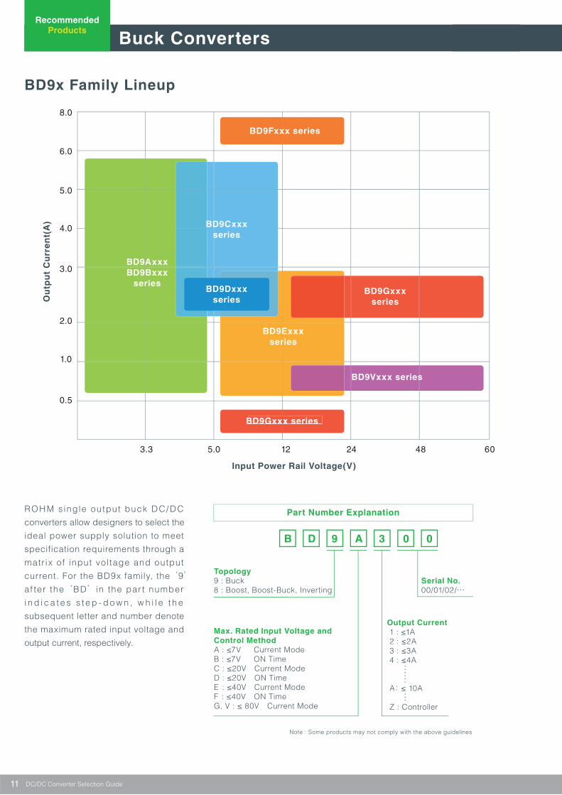
BD9x Family Lineup
ROHM single output buck DC/DC
converters allow designers to select the
ideal power supply solution to meet
specification requirements through a
matr ix of input vol tage and output
current. For the BD9x family, the ‘9’ af ter the ‘BD’ in the par t number
i n d i c a t e s s t e p - d o w n , w h i l e t h e
subsequent letter and number denote
the maximum rated input voltage and
output current, respectively.
11
BD9Gxxx シリーズ
Input Power Rail Voltage(V)
Ou
tpu
t C
urr
en
t(A
)
BD9Dxxx
series
BD9Exxx
series
BD9Cxxx
series
BD9Axxx
BD9Bxxx
series
BD9Gxxx シリーズ
BD9Gxxx
series
BD9Gxxx series
3.3
0.5
1.0
2.0
3.0
4.0
5.0
6.0
8.0
5.0 12 24 48 60
BD9Vxxx series
BD9Fxxx series
B D 9 A 3 0 0
Topology
9 : Buck8 : Boost, Boost-Buck, Inverting
Note : Some products may not comply with the above guidelines
Serial No.
00/01/02/・・・
Max. Rated Input Voltage and
Control Method
A : ≤7V Current ModeB : ≤7V ON TimeC : ≤20V Current ModeD : ≤20V ON TimeE : ≤40V Current ModeF : ≤40V ON TimeG, V : ≤ 80V Current Mode
Output Current
1 : ≤1A 2 : ≤2A 3 : ≤3A 4 : ≤4A
A: ≤ 10A
Z : Controller
Part Number Explanation
DC/DC Converter Selection Guide
Buck Converters
RecommendedProducts
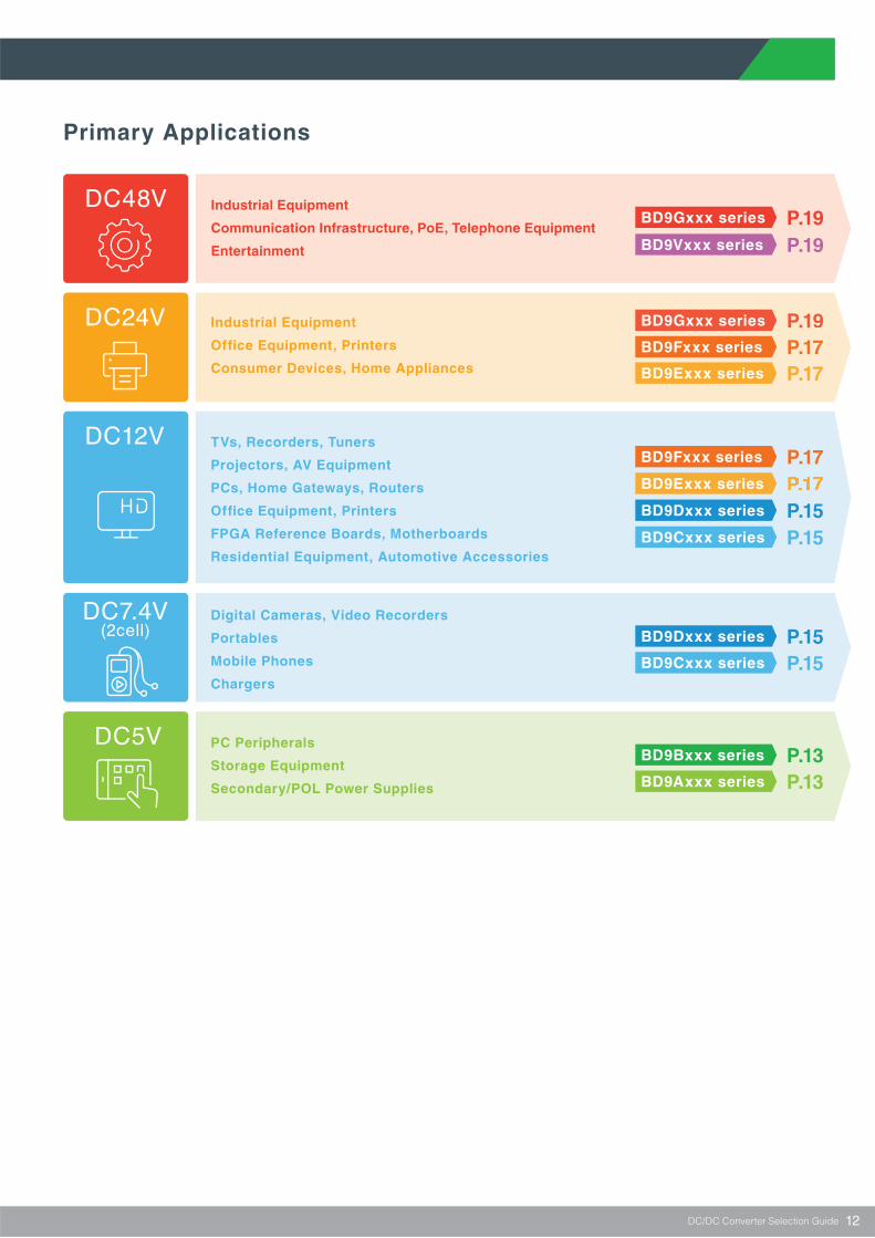
Primary Applications
12
DC48V Industrial Equipment
Communication Infrastructure, PoE, Telephone Equipment
Entertainment P.19BD9Vxxx series
P.19BD9Gxxx series
DC24V Industrial Equipment
Office Equipment, Printers
Consumer Devices, Home Appliances
P.19BD9Gxxx series
P.17BD9Fxxx series
P.17BD9Exxx series
DC7.4V(2cell)
Digital Cameras, Video Recorders
Portables
Mobile Phones
Chargers
P.15BD9Dxxx series
P.15BD9Cxxx series
DC5V PC Peripherals
Storage Equipment
Secondary/POL Power Supplies
P.13BD9Bxxx series
P.13BD9Axxx series
DC12V TVs, Recorders, Tuners
Projectors, AV Equipment
PCs, Home Gateways, Routers
Office Equipment, Printers
FPGA Reference Boards, Motherboards
Residential Equipment, Automotive Accessories
P.17BD9Fxxx series
BD9Exxx series
P.15BD9Dxxx series
P.15BD9Cxxx series
DC/DC Converter Selection Guide
3.3V/5V Input
BD9Axxx/BD9Bxxx series
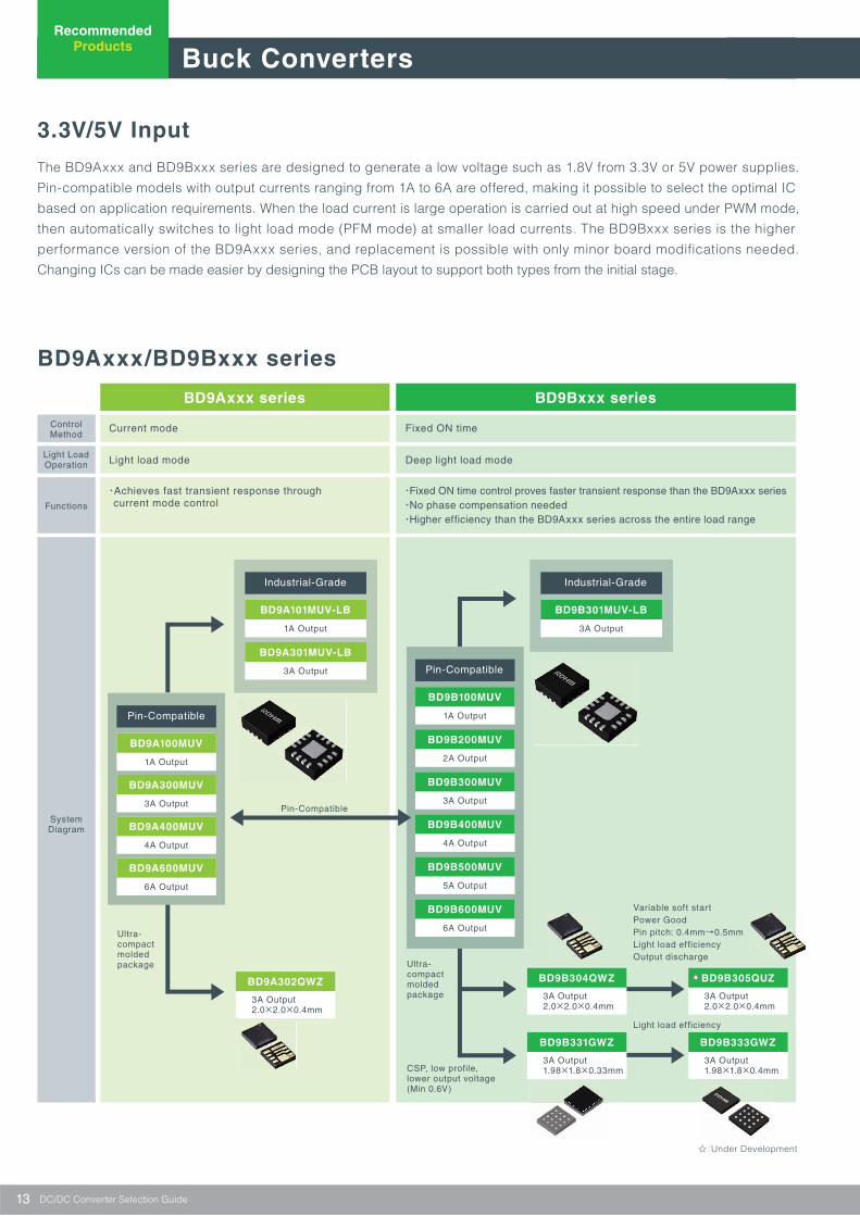
The BD9Axxx and BD9Bxxx series are designed to generate a low voltage such as 1.8V from 3.3V or 5V power supplies.
Pin-compatible models with output currents ranging from 1A to 6A are offered, making it possible to select the optimal IC
based on application requirements. When the load current is large operation is carried out at high speed under PWM mode,
then automatically switches to light load mode (PFM mode) at smaller load currents. The BD9Bxxx series is the higher
performance version of the BD9Axxx series, and replacement is possible with only minor board modifications needed.
Changing ICs can be made easier by designing the PCB layout to support both types from the initial stage.
13
BD9Axxx series
ControlMethod
Current mode
Functions
SystemDiagram
・Achieves fast transient response through current mode control
・Fixed ON time control proves faster transient response than the BD9Axxx series・No phase compensation needed・Higher efficiency than the BD9Axxx series across the entire load range
Fixed ON time
Light LoadOperation Light load mode Deep light load mode
BD9Bxxx series
Industrial-Grade
BD9A101MUV-LB
1A Output
Pin-Compatible
Industrial-Grade
BD9B301MUV-LB
3A Output
BD9A302QWZ
3A Output2.0×2.0×0.4mm
BD9B304QWZ
3A Output2.0×2.0×0.4mm
BD9B331GWZ
3A Output1.98×1.8×0.33mm
BD9B305QUZ
3A Output2.0×2.0×0.4mm
BD9B333GWZ
3A Output1.98×1.8×0.4mm
Pin-Compatible
BD9A100MUV
BD9A300MUV
BD9A400MUV
BD9A600MUV
Pin-Compatible
BD9B100MUV
1A Output
BD9B200MUV
2A Output
BD9B300MUV
3A Output
BD9B400MUV
4A Output
BD9B500MUV
5A Output
BD9B600MUV
6A Output
BD9A301MUV-LB
3A Output
Ultra-compactmoldedpackage
Ultra-compactmoldedpackage
Light load efficiency
Variable soft startPower GoodPin pitch: 0.4mm→0.5mmLight load efficiencyOutput discharge
CSP, low profile, lower output voltage(Min 0.6V)
☆:Under Development
DC/DC Converter Selection Guide
Buck Converters
RecommendedProducts
1A Output
3A Output
4A Output
6A Output
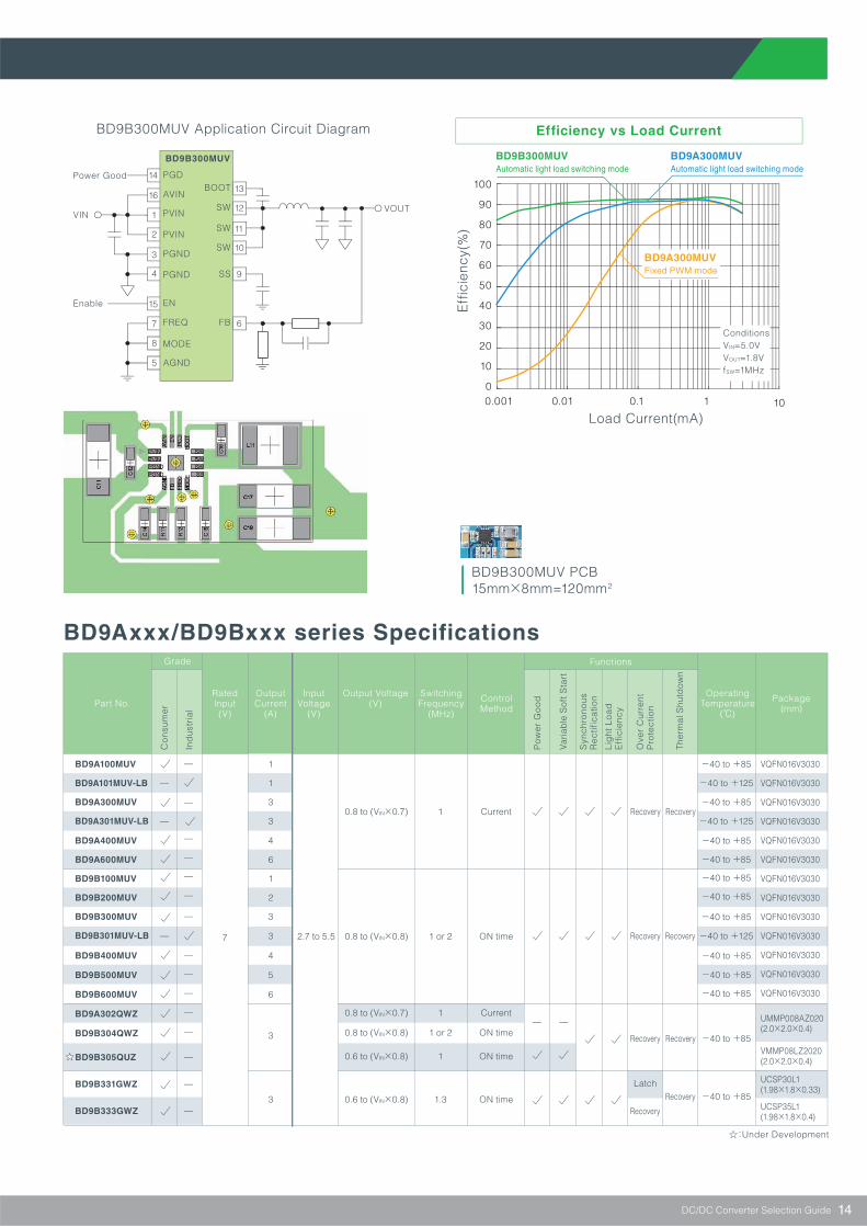
BD9Axxx/BD9Bxxx series Specifications
14
BD9B300MUV Application Circuit Diagram
PGD14
16
15
7
8
5
6
9
10
11
12
13
1
2
3
4
BOOT
SW
SW
SW
SS
FB
AVIN
PVIN
PVIN
PGND
PGND
EN
FREQ
Power Good
VIN
Enable
VOUT
MODE
AGND
BD9B300MUV
Efficiency vs Load Current
Eff
icie
ncy(
%)
Load Current(mA)
BD9A300MUVAutomatic light load switching mode
BD9B300MUVAutomatic light load switching mode
0.001 0.01 0.1 1 10
0
10
20
30
40
50
60
70
80
90
100
ConditionsVIN=5.0VVOUT=1.8VfSW=1MHz
BD9A300MUVFixed PWM mode
BD9A400MUV
BD9A600MUV
BD9B100MUV
BD9B200MUV
BD9B300MUV
BD9B301MUV-LB
BD9B400MUV
BD9B500MUV
BD9B600MUV
BD9A302QWZ
BD9B304QWZ
7
0.8 to (VIN×0.7)
0.8 to (VIN×0.8)
0.8 to (VIN×0.7)
0.8 to (VIN×0.8)
0.6 to (VIN×0.8)
0.6 to (VIN×0.8)
1
1
1 or 2
1
1 or 2
1.3
Current
Current
ON time
ON time
ON time
ON time
BD9A100MUV
BD9A101MUV-LB
BD9A300MUV
BD9A301MUV-LB
-40 to +85
-40 to +125
-40 to +85
-40 to +125
-40 to +85
-40 to +125
UMMP008AZ020(2.0×2.0×0.4)
VMMP08LZ2020(2.0×2.0×0.4)
UCSP30L1(1.98×1.8×0.33)
UCSP35L1(1.98×1.8×0.4)
-40 to +85
-40 to +85
-40 to +85
-40 to +85
-40 to +85
-40 to +85
-40 to +85
-40 to +85
-40 to +85
BD9B305QUZ
BD9B331GWZ
BD9B333GWZ
3
3
4
6
1
2
3
3
4
5
6
1
1
3
3
VQFN016V3030
VQFN016V3030
VQFN016V3030
VQFN016V3030
VQFN016V3030
VQFN016V3030
VQFN016V3030
VQFN016V3030
VQFN016V3030
VQFN016V3030
VQFN016V3030
VQFN016V3030
VQFN016V3030
Recovery Recovery
Recovery Recovery
Recovery
Recovery
Latch
Recovery
Recovery
BD9B300MUV PCB15mm×8mm=120mm2
2.7 to 5.5
☆:Under Development
DC/DC Converter Selection Guide
OperatingTemperature
(℃)
Package(mm)
Co
nsu
mer
Ind
ust
ria
l
Po
wer
Go
od
Syn
chro
no
usR
ec
tific
atio
n
Ove
r C
urre
ntP
rote
ctio
n
Ther
mal
Shu
tdow
n
Lig
ht L
oad
Eff
icie
nc
y
Var
iab
le S
oft
Sta
rt
Grade Functions
Part No.RatedInput(V)
OutputCurrent
(A)
InputVoltage
(V)
Output Voltage(V)
SwitchingFrequency
(MHz)
ControlMethod
12V Input
The BD9Cxxx and BD9Dxxx series are designed to generate voltages such as 3.3V or 5V from 12V power supplies. The
BD9Cxxx series consists of simple current mode buck converters. Pin-compatible models with output currents ranging from
3A to 6A are offered, making it possible to quickly replace the power supply even when the load current specifications change.
The BD9Dxx series of fixed ON time mode buck converters provides faster transient response than the BD9Cxxx series. In
addition, two types of power supplies, one featuring fixed PWM mode and the other integrating an automatic light load
switching mode, can be selected based on system specifications.
15
VIN
Enable
VOUT
8
5
1
3
2
6
7
4
BD9Cxxx/BD9Dxxx series
BD9Cxxx series
Current Mode
SystemDiagram
・Achieves fast transient response through
current mode control
・Fixed ON time control provides faster transient response than current mode control・No phase compensation needed・Light load operation ensures high efficiency across the entire load range
Fixed ON time
With and without
BD9Dxxx series
Industrial-Grade
BD9C301FJ-LB
BD9D321EFJ Application Circuit Diagram
Pin-Compatible
BD9C301FJ
BD9C401EFJ
BD9C501EFJ
BD9C601EFJ
Pin-Compatible
BD9D321EFJ
3A OutputLight Load Mode
Light Load Mode
Ultra-compacmolded package
Pin-Compatible
BD9D322QWZ
3A Output2.0×2.0×0.4mmLight Load Mode
Light Load Mode
BD9D323QWZ
3A Output2.0×2.0×0.4mm
BD9D321EFJ
VIN BOOT
SW
FB
GND
EN
VREG
SS
VIN
Enable
VOUT2
1
6
3 4
5
7
8
BD9C301FJ Application Circuit Diagram
VIN SW
SW
COMP
FB
PGND
EN
AGND
BD9C301FJ
DC/DC Converter Selection Guide
Buck Converters
RecommendedProducts
ControlMethod
Functions
Light LoadOperation
3A Output
3A Output
4A Output
5A Output
6A Output
BD9D320EFJ
3A Output
16
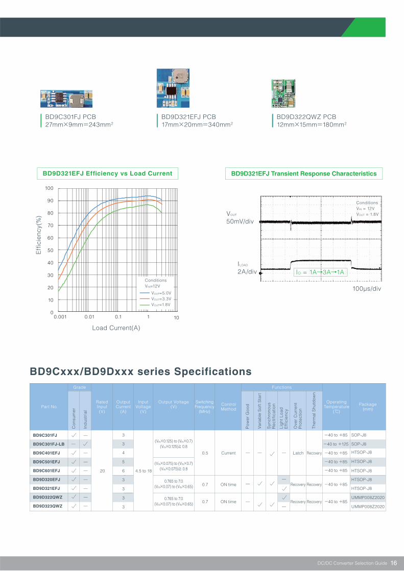
BD9C301FJ PCB27mm×9mm=243mm2
BD9D321EFJ PCB17mm×20mm=340mm2
BD9D322QWZ PCB12mm×15mm=180mm2
VOUT
50mV/div
ILOAD
2A/div
100µs/div
BD9D321EFJ Transient Response CharacteristicsBD9D321EFJ Efficiency vs Load Current
ConditionsVIN = 12VVOUT = 1.8V
IO = 1A→3A→1A
Eff
icie
ncy(
%)
Load Current(A)
0.001 0.01 0.1 1 100
10
20
30
40
50
60
70
80
90
100
ConditionsVIN=12V
VOUT=5.0VVOUT=3.3VVOUT=1.8V
DC/DC Converter Selection Guide
BD9Cxxx/BD9Dxxx series Specifications
Part No.RatedInput(V)
OutputCurrent
(A)
InputVoltage
(V)
Output Voltage(V)
OperatingTemperature
(℃)
Package(mm)
SwitchingFrequency
(MHz)
ControlMethod
Grade Functions
BD9C301FJ
BD9C301FJ-LB
BD9C401EFJ
BD9C501EFJ
BD9C601EFJ
BD9D320EFJ
BD9D321EFJ
BD9D322QWZ
BD9D323QWZ
(VIN×0.125) to (VIN×0.7)(VIN×0.125)≧ 0.8
(VIN×0.075) to (VIN×0.7)(VIN×0.075)≧ 0.8
0.765 to 7.0(VIN×0.07) to (VIN×0.65)
0.765 to 7.0(VIN×0.07) to (VIN×0.65)
0.5
0.7
0.7
Current
ON time
ON timeHTSOP-J8
HTSOP-J8
UMMP008Z2020
UMMP008Z2020
-40 to +85
-40 to +125
-40 to +85
-40 to +85
-40 to +85
-40 to +85
-40 to +85
4
5
6
3
3
3
3
3
3
HTSOP-J8
HTSOP-J8
HTSOP-J8
SOP-J8
SOP-J8
Latch Recovery
Recovery Recovery
Recovery Recovery
20 4.5 to 18
Co
nsu
mer
Ind
ustr
ial
Po
wer
Go
od
Syn
chro
no
usR
ec
tific
atio
n
Ove
r C
urre
ntP
rote
ctio
n
Ther
mal
Shu
tdow
n
Lig
ht L
oad
Eff
icie
nc
y
Var
iab
le S
oft
Sta
rt
24V Input
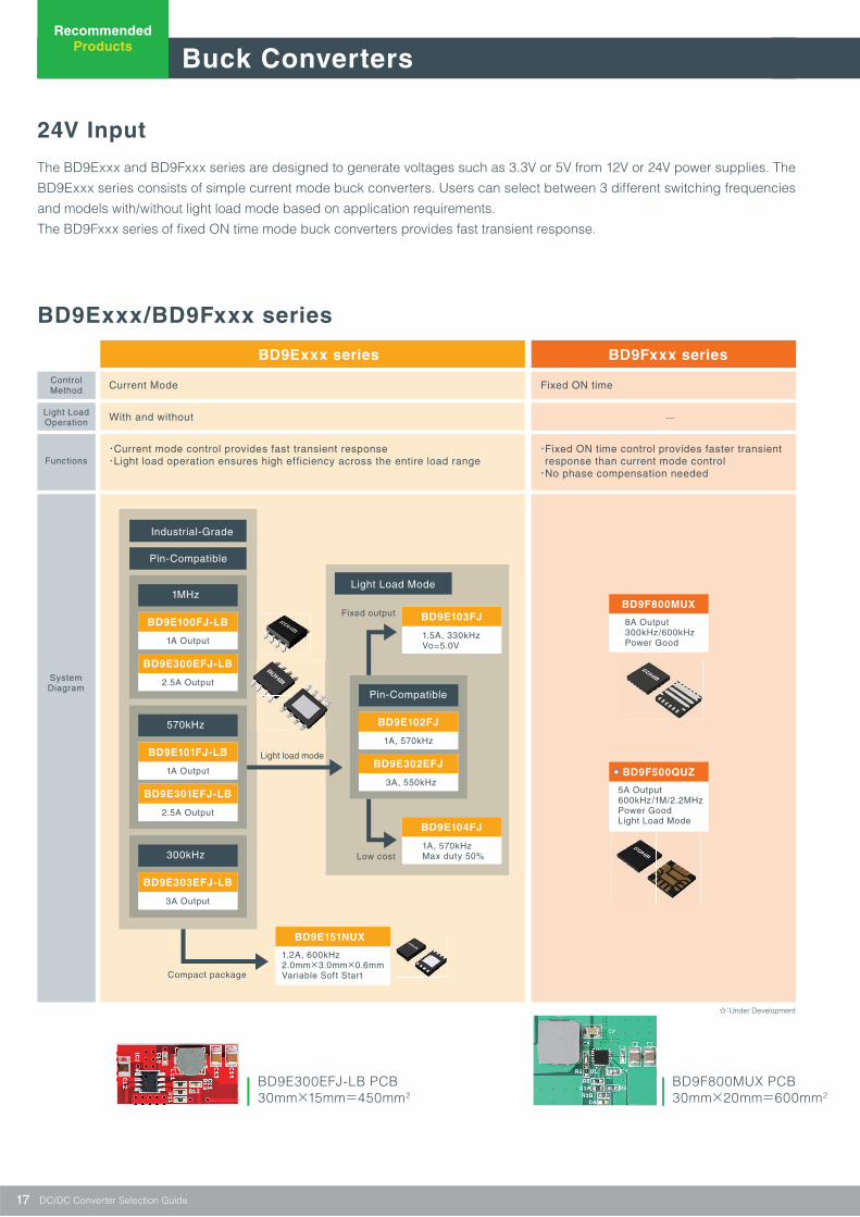
The BD9Exxx and BD9Fxxx series are designed to generate voltages such as 3.3V or 5V from 12V or 24V power supplies. The
BD9Exxx series consists of simple current mode buck converters. Users can select between 3 different switching frequencies
and models with/without light load mode based on application requirements.
The BD9Fxxx series of fixed ON time mode buck converters provides fast transient response.
17
BD9Exxx/BD9Fxxx series
BD9Exxx series
Current Mode
・Current mode control provides fast transient response・Light load operation ensures high efficiency across the entire load range
・Fixed ON time control provides faster transient response than current mode control・No phase compensation needed
Fixed ON time
With and without
BD9Fxxx series
Industrial-Grade
Light Load Mode
Pin-Compatible
Compact package
Low cost
Fixed output
Light load mode
1MHz
BD9E100FJ-LB
BD9E300EFJ-LB
570kHz
BD9E101FJ-LB
BD9E301EFJ-LB
Pin-Compatible
BD9E102FJ
1A, 570kHz
BD9E302EFJ
3A, 550kHz
BD9E104FJ
1A, 570kHzMax duty 50%
BD9E103FJ
1.5A, 330kHzVo=5.0V
300kHz
BD9E303EFJ-LB
BD9E300EFJ-LB PCB30mm×15mm=450mm2
BD9F800MUX PCB30mm×20mm=600mm2
BD9E151NUX
1.2A, 600kHz2.0mm×3.0mm×0.6mmVariable Soft Start
BD9F800MUX
8A Output300kHz/600kHzPower Good
BD9F500QUZ
5A Output600kHz/1M/2.2MHzPower GoodLight Load Mode
☆:Under Development
DC/DC Converter Selection Guide
Buck Converters
RecommendedProducts
SystemDiagram
ControlMethod
Functions
Light LoadOperation
1A Output
2.5A Output
1A Output
2.5A Output
3A Output
18
VIN
VOUT
Enable
1
2
7
8
6
5
3
4
BOOT SW
COMP
FB
VIN
PGND
EN
AGND
Efficiency vs Load Current
Selectable based on system requirements
BD9Exxx/BD9Fxxx series Specifications
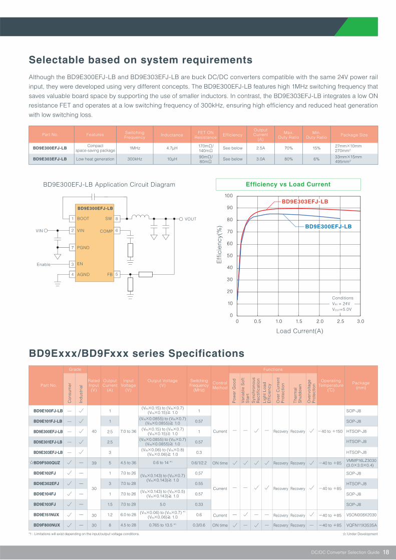
Although the BD9E300EFJ-LB and BD9E303EFJ-LB are buck DC/DC converters compatible with the same 24V power rail
input, they were developed using very different concepts. The BD9E300EFJ-LB features high 1MHz switching frequency that
saves valuable board space by supporting the use of smaller inductors. In contrast, the BD9E303EFJ-LB integrates a low ON
resistance FET and operates at a low switching frequency of 300kHz, ensuring high efficiency and reduced heat generation
with low switching loss.
BD9E300EFJ-LB
BD9E303EFJ-LB
Part No.
Low heat generation
Compactspace-saving package
Features
1MHz
300kHz
SwitchingFrequency
70%
80%
Max.Duty Ratio
15%
6%
Min.Duty Ratio
170mΩ/140mΩ90mΩ/80mΩ
FET ONResistance
27mm×10mm270mm2
33mm×15mm495mm2
Package Size
4.7µH
10µH
Inductance
See below
See below
Efficiency
2.5A
3.0A
OutputCurrent
(A)
Load Current(A)
Eff
icie
ncy(
%)
0 0.5 1.0 1.5 2.0 2.5 3.00
10
20
30
40
50
60
70
80
90
100
ConditionsVIN = 24VVOUT=5.0V
BD9E303EFJ-LB
BD9E300EFJ-LB
BD9E300EFJ-LB Application Circuit Diagram
BD9E300EFJ-LB
DC/DC Converter Selection Guide
Grade
40 7.0 to 36
39
30
30
30
Current -40 to +150
ON time -40 to +85
Current -40 to +85
Current -40 to +85
ON time -40 to +85
*1 : Limitations will exist depending on the input/output voltage conditions.
(VIN×0.15) to (VIN×0.7)(VIN×0.15)≧ 1.0
(VIN×0.0855) to (VIN×0.7)(VIN×0.0855)≧ 1.0
(VIN×0.15) to (VIN×0.7)(VIN×0.15)≧ 1.0
(VIN×0.0855) to (VIN×0.7)(VIN×0.0855)≧ 1.0
(VIN×0.06) to (VIN×0.8)(VIN×0.06)≧ 1.0
(VIN×0.143) to (VIN×0.7)(VIN×0.143)≧ 1.0
(VIN×0.143) to (VIN×0.5)(VIN×0.143)≧ 1.0
(VIN×0.06) to (VIN×0.7) *1
(VIN×0.06)≧ 1.0
0.765 to 13.5 *1
5.0
0.6 to 14 *1
Functions
Recovery
Recovery
Recovery
Recovery
Recovery
Recovery
Recovery
Recovery
Recovery
Recovery
BD9E100FJ-LB
BD9E101FJ-LB
BD9E300EFJ-LB
BD9E301EFJ-LB
BD9E303EFJ-LB
BD9F500QUZ
BD9E102FJ
BD9E302EFJ
BD9E104FJ
BD9E103FJ
BD9E151NUX
BD9F800NUX
1
0.57
1
0.57
0.3
0.6/1/2.2
0.57
0.55
0.57
0.33
0.6
0.3/0.6
1
1
2.5
2.5
3
5
1
3
1
1.5
1.2
8
4.5 to 36
7.0 to 26
7.0 to 28
7.0 to 26
7.0 to 28
6.0 to 28
4.5 to 28
SOP-J8
SOP-J8
HTSOP-J8
HTSOP-J8
HTSOP-J8
VMMP16LZ3030(3.0×3.0×0.4)
SOP-J8
HTSOP-J8
SOP-J8
SOP-J8
VSON008X2030
VQFN11X3535A
☆:Under Development
Co
nsu
mer
Ind
ustr
ial
Po
wer
Go
od
Syn
chro
no
usR
ec
tific
atio
n
Ove
r C
urre
ntP
rote
ctio
n
Ther
mal
Shu
tdow
n
Ove
rvol
tag
eP
rote
ctio
n
Lig
ht L
oad
Eff
icie
nc
y
Va
ria
ble
So
ftS
tart
Part No.RatedInput(V)
OutputCurrent
(A)
InputVoltage
(V)
OperatingTemperature
(℃)
SwitchingFrequency
(MHz)
ControlMethod
Output Voltage(V) Package
(mm)
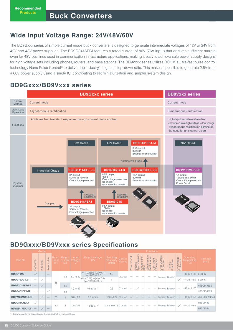
The BD9Gxxx series of simple current mode buck converters is designed to generate intermediate voltages of 12V or 24V from
42V and 48V power supplies. The BD9G341AEFJ features a rated current of 80V (76V input) that ensures sufficient margin
even for 48V bus lines used in communication infrastructure applications, making it easy to achieve safe power supply designs
for high voltage sets including phones, routers, and base stations. The BD9Vxxx series utilizes ROHM’s ultra-fast pulse control
technology Nano Pulse Control® to deliver the industry’s highest step-down ratio. This makes it possible to generate 2.5V from
a 60V power supply using a single IC, contributing to set miniaturization and simpler system design.
19
BD9Gxxx series
Current mode
・Achieves fast transient response through current mode control ・High step-down ratio enables direct conversion from high voltage to low voltage・Synchronous rectification eliminates the need for an external diode
Current mode
Asynchronous rectification Synchronous rectification
BD9Vxxx series
Industrial-Grade
Compact
Industrialequipment
Industrialequipment
45V Rated 70V RatedBD9G401EFJ-M
3.5A output300kHzExternal synchronization
80V Rated
BD9V101MUF-LB
1A output1.9MHz to 2.3MHzOvervoltage protectionPower Good
BD9G341AEFJ-LB
3A output50kHz to 750kHzOvervoltage protection
BD9G201EFJ-LB
1.5A output300kHzExternal synchronization
BD9G341AEFJ
3A output50kHz to 750kHzOvervoltage protection
Automotive-grade
BD9G101G
0.5A output1.5MHzNo phasecompensation needed
BD9G102G-LB
0.5A output1MHzOvervoltage protectionNo phasecompensation needed
BD9Gxxx/BD9Vxxx series SpecificationsFunctionsGrade
BD9G101G
BD9G102G-LB
BD9G201EFJ-LB
BD9G401EFJ-M
BD9V101MUF-LB
BD9G341AEFJ
BD9G341AEFJ-LB
1.5
1
0.3
45
0.5 Current Recovery
Recovery
Recovery
Recovery
Recovery
Recovery
Recovery
Recovery
Current
6.0 to 42
(VIN×0.15) to (VIN×0.7)(VIN×0.15)≧ 1.0
(VIN×0.08) to (VIN×0.8)(VIN×0.08)≧ 0.75
0.8 to VIN *1
-40 to +105
-40 to +85
SSOP6
SSOP6
HTSOP-J8ES
HTSOP-J8ES
VQFN24FV4040
HTSOP-J8
HTSOP-J8
-40 to +105
-40 to +85
-40 to +150
1.0 to VIN *1
*1 : Limitations will exist depending on the input/output voltage conditions.
4.5 to 42
Current
Current
1.5
3.5
1
380
0.8 to 5.516 to 60
12 to 76
1.9 to 2.3
0.05 to 0.75
70
Wide Input Voltage Range: 24V/48V/60V
BD9Gxxx/BD9Vxxx series
DC/DC Converter Selection Guide
Buck Converters
RecommendedProducts
SystemDiagram
ControlMethod
Functions
Light LoadOperation
Co
nsu
mer
Ind
ustr
ial
Au
tom
otiv
e
Po
wer
Go
od
Ext
erna
lS
ynch
roni
zatio
n
Syn
chro
no
usR
ec
tific
atio
n
Ove
r C
urre
ntP
rote
ctio
n
Ther
mal
Shu
tdow
n
Ove
rvol
tag
eP
rote
ctio
n
Lig
ht L
oad
Eff
icie
nc
y
Va
ria
ble
So
ftS
tart
RatedInput(V)
OutputCurrent
(A)
InputVoltage
(V)
Output Voltage(V)
OperatingTemperature
(℃)
ControlMethod
Package(mm)
SwitchingFrequency
(MHz)Part No.
20
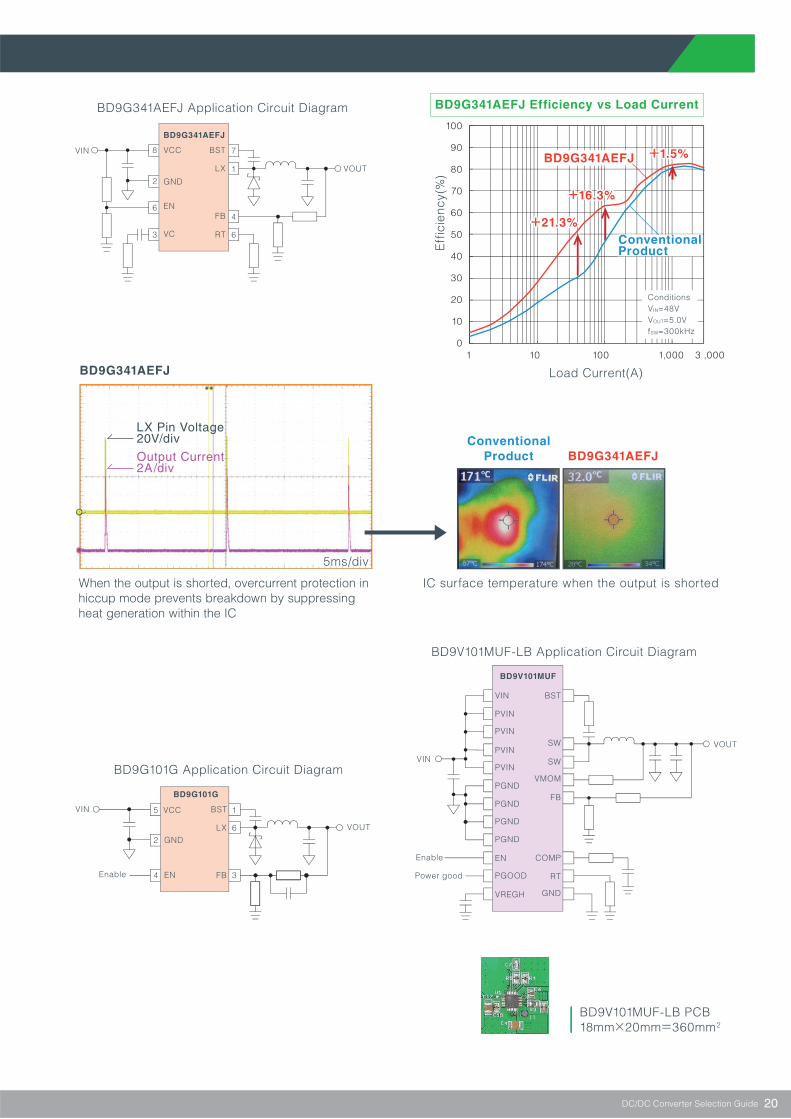
BD9G341AEFJ Efficiency vs Load Current
5ms/div
LX Pin Voltage20V/div
Output Current2A/div
IC surface temperature when the output is shorted
BD9G341AEFJ
Conventional
Product
VIN
VOUT
8 7
1
4
6
2
6
3
VCC BST
LX
FB
RT
GND
EN
VC
BD9V101MUF-LB PCB18mm×20mm=360mm2
BD9G341AEFJ
When the output is shorted, overcurrent protection inhiccup mode prevents breakdown by suppressingheat generation within the IC
VIN
VIN
VOUT
VOUT
5 1
6
3
2
4
BD9G101G Application Circuit Diagram
Enable
Enable
Power good
VCC BST
LX
FB
GND
EN
BD9V101MUF-LB Application Circuit Diagram
VIN BST
SW
SW
VMOM
FB
COMP
RT
GND
PVIN
PVIN
PVIN
PVIN
PGND
PGND
PGND
PGND
EN
PGOOD
VREGH
Eff
icie
ncy(
%)
Load Current(A)
10
10
20
30
40
50
60
70
80
90
100
10 100 1,000 3 ,000
ConditionsVIN=48VVOUT=5.0VfSW=300kHz
+1.5%+1.5%
ConventionalProduct
+21.3%+21.3%
+16.3%+16.3%
BD9G341AEFJ +1.5%
+21.3%
+16.3%
BD9G341AEFJ
BD9G341AEFJ Application Circuit Diagram
BD9V101MUF
BD9G101G
DC/DC Converter Selection Guide
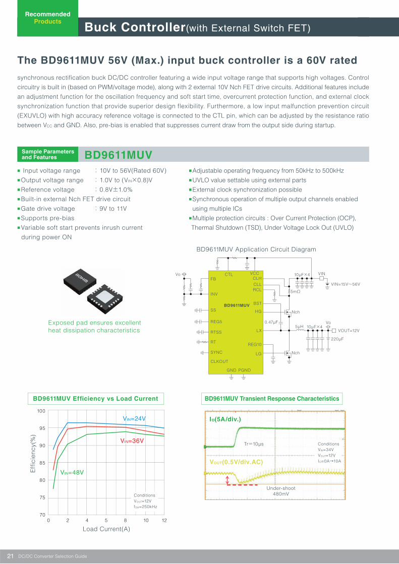
The BD9611MUV 56V (Max.) input buck controller is a 60V rated
synchronous rectification buck DC/DC controller featuring a wide input voltage range that supports high voltages. Control
circuitry is built in (based on PWM/voltage mode), along with 2 external 10V Nch FET drive circuits. Additional features include
an adjustment function for the oscillation frequency and soft start time, overcurrent protection function, and external clock
synchronization function that provide superior design flexibility. Furthermore, a low input malfunction prevention circuit
(EXUVLO) with high accuracy reference voltage is connected to the CTL pin, which can be adjusted by the resistance ratio
between VCC and GND. Also, pre-bias is enabled that suppresses current draw from the output side during startup.
21
■ Input voltage range : 10V to 56V(Rated 60V)■ Output voltage range : 1.0V to (VIN×0.8)V■ Reference voltage : 0.8V±1.0%■ Built-in external Nch FET drive circuit ■ Gate drive voltage : 9V to 11V■ Supports pre-bias■ Variable soft start prevents inrush current
during power ON
■ Adjustable operating frequency from 50kHz to 500kHz■ UVLO value settable using external parts■ External clock synchronization possible■ Synchronous operation of multiple output channels enabled
using multiple ICs■ Multiple protection circuits : Over Current Protection (OCP),
Thermal Shutdown (TSD), Under Voltage Lock Out (UVLO)
BD9611MUV
Exposed pad ensures excellent heat dissipation characteristics
BD9611MUV Efficiency vs Load Current BD9611MUV Transient Response Characteristics
Eff
icie
ncy(
%)
Load Current(A)0 2 4 5 8 10 12
70
75
80
85
90
95
100
ConditionsVOUT=12VfSW=250kHz
BD9611MUV Application Circuit Diagram
CTL VCCCLHCLLRCL
BST
HG
LX
REG10
LG
FB
INV
SS
REG5
RTSS
RT
SYNC
CLKOUT
GND PGND
BD9611MUV
Vo
Nch
220µF
5µH0.47µF
Nch
5mΩ
10µF×4
10µF×4 VIN
VIN=15V~56V
Vo
VOUT=12V
VVININ=24V=24V
VININ=36V=36V
VININ=48V=48V
VIN=24V
VIN=36V
VIN=48V
IO(5A/div.)
VOUT(0.5V/div.AC)
Tr=10µs
Under-shoot480mV
ConditionsVIN=34VVOUT=12VIO=0A→10A
Buck Controller(with External Switch FET)
RecommendedProducts
Sample Parametersand Features
DC/DC Converter Selection Guide
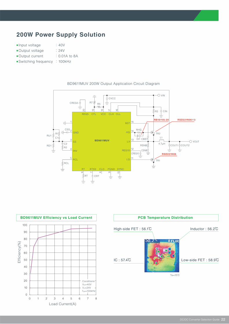
200W Power Supply Solution
22
■ Input voltage : 40V■ Output voltage : 24V■ Output current : 0.01A to 8A■ Switching frequency : 100kHz
PCB Temperature DistributionBD9611MUV Efficiency vs Load Current
RSD221N06×3RB161VA-20
RSD221N06
BD9611MUV 200W Output Application Circuit Diagram
BD9611MUV
REG5 CTL VCC CLH CLL
BST
HG
LX
REG10
LG
SYNCPGNDCLORTSSRT
RCL
INV
SS
GNDCSS
CREG5
CREG10
C2
R2
R7 R5
CVCCVIN
CINRS
TR2
TR1
L1
COUT1
VOUT
COUT2
RHG
DI1 CBST
RSNB
CSNB
R1
C1
RCL
RT CRT
RD1
RU1
4.7µH
11
12
13
14
15
5
620 19 18 17 16
7 8 9 10
4
3
2
1
High-side FET : 56.1℃
IC : 57.4℃
Inductor : 56.2℃
Low-side FET : 58.9℃
Ta=25℃
Eff
icie
ncy(
%)
Load Current(A)
ConditionsVIN=40VVO=24VfSW=100kHz
0 1 2 3 4 5 6 7 80
10
20
30
40
50
60
70
80
90
100
DC/DC Converter Selection Guide
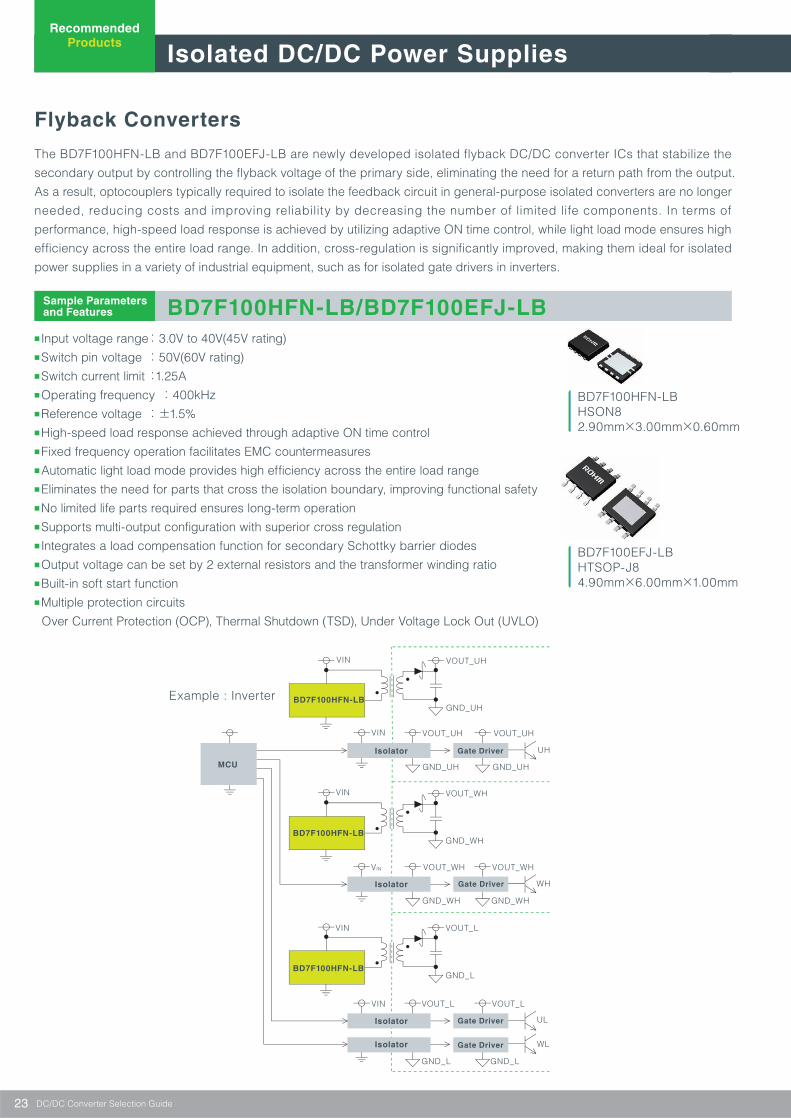
Flyback Converters
The BD7F100HFN-LB and BD7F100EFJ-LB are newly developed isolated flyback DC/DC converter ICs that stabilize the
secondary output by controlling the flyback voltage of the primary side, eliminating the need for a return path from the output.
As a result, optocouplers typically required to isolate the feedback circuit in general-purpose isolated converters are no longer
needed, reducing costs and improving reliability by decreasing the number of limited life components. In terms of
performance, high-speed load response is achieved by utilizing adaptive ON time control, while light load mode ensures high
efficiency across the entire load range. In addition, cross-regulation is significantly improved, making them ideal for isolated
power supplies in a variety of industrial equipment, such as for isolated gate drivers in inverters.
23
Isolated DC/DC Power Supplies
RecommendedProducts
■ Input voltage range : 3.0V to 40V(45V rating)■ Switch pin voltage : 50V(60V rating)■ Switch current limit :1.25A■ Operating frequency : 400kHz■ Reference voltage : ±1.5%■ High-speed load response achieved through adaptive ON time control■ Fixed frequency operation facilitates EMC countermeasures■ Automatic light load mode provides high efficiency across the entire load range■ Eliminates the need for parts that cross the isolation boundary, improving functional safety■ No limited life parts required ensures long-term operation■ Supports multi-output configuration with superior cross regulation■ Integrates a load compensation function for secondary Schottky barrier diodes■ Output voltage can be set by 2 external resistors and the transformer winding ratio■ Built-in soft start function■ Multiple protection circuits
Over Current Protection (OCP), Thermal Shutdown (TSD), Under Voltage Lock Out (UVLO)
BD7F100HFN-LB/BD7F100EFJ-LB
BD7F100HFN-LBHSON82.90mm×3.00mm×0.60mm
BD7F100EFJ-LBHTSOP-J84.90mm×6.00mm×1.00mm
Example : Inverter
MCU
BD7F100HFN-LB
VIN
VIN
VIN
VOUT_UH
GND_UH
VOUT_UH
VOUT_WH
GND_WH
VIN VOUT_WH VOUT_WH
GND_WH
VOUT_LVIN
GND_L
VIN VOUT_L
GND_L GND_L
UL
WL
VOUT_L
GND_WH
WH
VOUT_UH
GND_UH GND_UH
UH
BD7F100HFN-LB
BD7F100HFN-LB
Isolator
Isolator
Isolator
Isolator
Gate Driver
Gate Driver
Gate Driver
Gate Driver
DC/DC Converter Selection Guide
Sample Parametersand Features

24
BD9F100HFN-LB
Max. Output Power vs Input Supply Voltage
Effects of ROHM's Load Compensation Function
BD7F100HFN-LB Evaluation BoardBD7F100HFN-LB Application Circuit Diagram 24V→5VVIN24V
VIN
BD7F100HFN-LB
SDX/EN
COMP
AGND REF PGND
SW
FB
10µF63µH
3:1
1:2
7µH47µF
VOUT -
VOUT+5V,1A
3.9kΩ
SBD
SBD
The load compensation function corrects output voltage drops due to the Vf characteristics of the secondary Schottky barrier diode depending on the load current
VIN5V
10µF 22µF40µH10µH
3.9kΩ
SBD
SBD
33
BD7F100HFN-LB Application Circuit Diagram 5V→5V
BD7F100HFN-LB
VIN
SDX/EN
COMP
AGND REF PGND
SW
FB
VOUT-
VOUT+15V, 240mA
Ma
x. O
utp
ut P
ower
(W)
Input Supply Voltage(V)
00
1
2
3
4
5
6
7
8
5 10 15 20 25 30 35 40 45 50
Out
put
Vol
tag
e (
V)
Load Current(mA)
04.75
4.80
4.85
4.90
4.95
5.00
5.05
5.10
5.15
5.20
5.25
200 400 600 800 1,000
ConditionsVIN = 24VVOUT = 5.0V
1:1:1BD7F100HFN-LB Application Circuit Diagram 24V→±15V
BD7F100HFN-LB
VIN24V
10µF 10µF
10µF
50µH
50µH
50µH
COM
VOUT+15V,220mA
3.9kΩ
SBD
SBD
SBD
VIN
SDX/EN
COMP
AGND REF PGND
SW
FB
With load compensation
Without load compensation
VOUT--15V, -220mA
DC/DC Converter Selection Guide
25
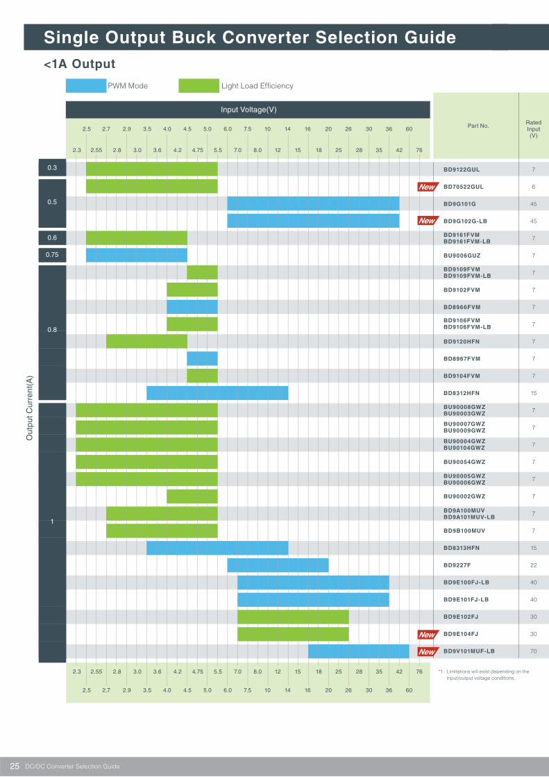
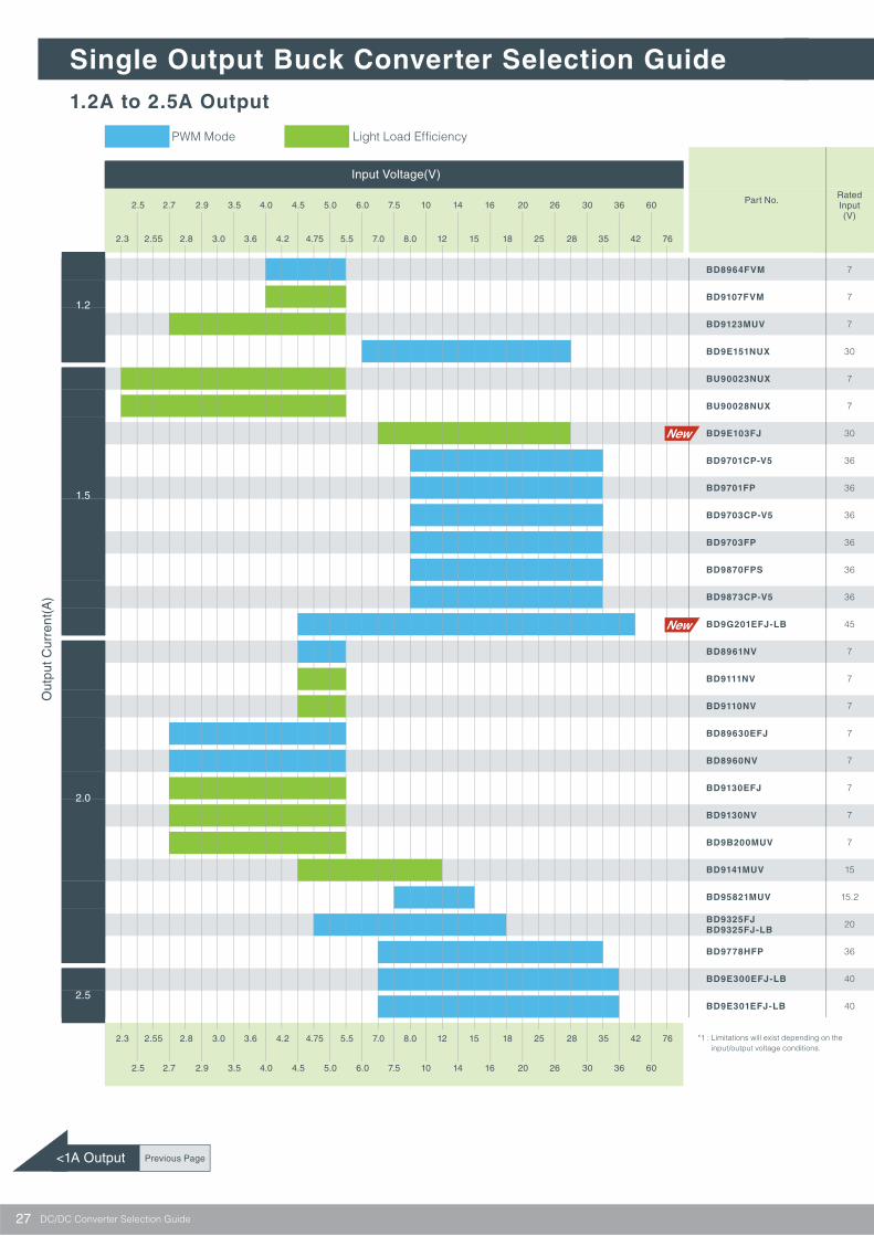
Single Output Buck Converter Selection Guide
PWM Mode Light Load Efficiency
Input Voltage(V)
0.3
0.5
0.6
0.75
0.8
1
Out
put C
urre
nt(A
)
7
6
45
45
7
7
7
7
7
7
7
7
7
15
7
7
7
7
7
7
7
7
15
22
40
40
30
30
70
BD9122GUL
BD70522GUL
BD9G101G
BD9G102G-LB
BU9006GUZ
BD9102FVM
BD8966FVM
BD9120HFN
BD8967FVM
BD9104FVM
BD8312HFN
BU90054GWZ
BU90002GWZ
BD9B100MUV
BD8313HFN
BD9227F
BD9E100FJ-LB
BD9E101FJ-LB
BD9E102FJ
BD9E104FJ
BD9V101MUF-LB
*1 : Limitations will exist depending on the input/output voltage conditions.
BD9161FVMBD9161FVM-LB
BD9109FVMBD9109FVM-LB
BD9106FVMBD9106FVM-LB
BU90008GWZBU90003GWZ
BU90007GWZBU90009GWZ
BU90004GWZBU90104GWZ
BU90005GWZBU90006GWZ
BD9A100MUVBD9A101MUV-LB
2.5 2.7 2.9 3.5 4.0 4.5 5.0 6.0 7.5 10 14 16 20 26 30 36 60
2.3 2.55 2.8 3.0 3.6 4.2 4.75 5.5 7.0 8.0 12 15 18 25 28 35 42 76
2.3 2.55 2.8 3.0 3.6 4.2 4.75 5.5 7.0 8.0 12 15 18 25 28 35 42 76
2.5 2.7 2.9 3.5 4.0 4.5 5.0 6.0 7.5 10 14 16 20 26 30 36 60
<1A Output
DC/DC Converter Selection Guide
RatedInput(V)
Part No.
26
0.3
0.5
0.5
0.5
0.6
0.75
0.8
0.8
0.8
0.8
0.8
0.8
0.8
0.8
1
1
1
1
1
1
1
1
1
1
1
1
1
1
1
2.5
2.5
6
6
2.5
2.5
4.5
4
4
4
2.7
4.5
4.5
3.5
2.3
2.3
2.3
2.3
2.3
4
2.7
2.7
3.5
6
7
7
7
7
16
5.5
5.5
42
42
4.5
4.5
5.5
5.5
5.5
5.5
4.5
5.5
5.5
14
5.5
5.5
5.5
5.5
5.5
5.5
5.5
5.5
14
20
36
36
26
26
60
to
to
to
to
to
to
to
to
to
to
to
to
to
to
to
to
to
to
to
to
to
to
to
to
to
to
to
to
to
1
1
1.5
1
1
2
1
1
1
1
1
1
1
1.5
5.4
5.4
6
6
1
1 or 2
1
1
1
0.57
0.57
0.57
1.9 to 2.3
Functions
Pow
er G
oo
d
Ext
erna
lS
ynch
ron
izat
ion
Var
iabl
e S
oft S
tart
Syn
chro
no
us
Re
ctifi
catio
n
Lig
ht L
oad
Eff
icie
ncy
Ove
r Cur
rent
Pro
tect
ion
The
rmal
Shu
tdow
n
Current
ON time
Current
Current
Current
Current
Current
Current
Current
Current
Current
Current
Current
Voltage
ON time
ON time
ON time
ON time
ON time
ON time
Current
ON time
Voltage
Current
Current
Current
Current
Current
Current
SSOP6
SSOP6
MSOP8
MSOP8
MSOP8
MSOP8
MSOP8
HSON8
MSOP8
MSOP8
HSON8
VQFN016V3030
VQFN016V3030
HSON8
SOP8
SOP-J8
SOP-J8
SOP-J8
SOP-J8
VQFN24FV4040
Latch
Recovery
Recovery
Recovery
Latch
Recovery
Latch
Latch
Latch
Latch
Latch
Latch
Latch
Recovery
Recovery
Recovery
Recovery
Recovery
Recovery
Recovery
Recovery
Recovery
Recovery
Recovery
Recovery
Recovery
Recovery
Latch
Recovery
Recovery
Recovery
Latch
Recovery
Latch
Latch
Latch
Latch
Latch
Latch
Latch
Recovery
Recovery
Recovery
Recovery
Recovery
Recovery
Recovery
Recovery
Recovery
Recovery
Recovery
Recovery
Recovery
Recovery
Recovery
Recovery
1.0 to 2.0
1.2 to 3.3*1
1.0 to 3.3
0.95 to VIN
3.3
1.24
1.0 to 2.5
1.0 to 2.5
1.0 to 1.5
3.3
3.3
1.2 to 12.0
1.8
1.8
3.3
0.8 to (VIN×0.7)
0.8 to (VIN×0.8)
1.2 to 12.0
0.8 to 5.5
Max. output capacitance10µF
100% duty
(VIN×0.15) to (VIN×0.7)(VIN×0.15)≧1.0
(VIN×0.008) to (VIN×0.8)(VIN×0.008)≧0.75
1.01.2
3.64
44.2
1.251.3
2.53.0
(VIN×0.252) to VIN
(VIN×0.252)≧1.0
(VIN×0.15) to (VIN×0.7)(VIN×0.15)≧1.0
(VIN×0.0855) to (VIN×0.7)(VIN×0.0855)≧1.0
(VIN×0.143) to (VIN×0.7)(VIN×0.143)≧1.0
(VIN×0.143) to (VIN×0.5)(VIN×0.143)≧1.0
Ove
r Vol
tage
Pro
tect
ion
Output discharge, 100% duty, output voltage settingvia pin selection
VCSP50L2(2.5×1.1)
VCSP50L1C(1.76×1.56×0.57)
VCSP35L1(1.6×1.6×0.4)
UCSP35L1(1.3×0.9×0.4)
UCSP35L1(1.3×0.9×0.4)
UCSP35L1(1.3×0.9×0.4)
UCSP30L1(1.3×0.9×0.33)
UCSP35L1(1.3×0.9×0.4)
UCSP35L1(1.3×0.9×0.4)
Built-in input/output bypass switch, 100% duty
Max. output capacitance10µFMax. output capacitance100µF
>1.2A Output
DC/DC Converter Selection Guide
OutputCurrent
(A)
Input Voltage(V)
SwitchingFrequency
(MHz)
ControlMethod
Other Functions
-25 to +85
-40 to +85
-40 to +105
-40 to +85
-25 to +85
-35 to +85
-25 to +85
-25 to +85
-25 to +85
-25 to +85
-25 to +85
-25 to +85
-25 to +85
-25 to +85
-40 to +85
-40 to +85
-40 to +85
-40 to +85
-40 to +85
-40 to +85
-40 to +85
-40 to +85
-40 to +85
-40 to +150
-40 to +150
-40 to +85
-40 to +85
-40 to +150
-40 to +85
-40 to +125
OperatingTemperature
(℃)
Package(mm)
Output Voltage(V)
Next Page
27
Single Output Buck Converter Selection Guide
2.5 2.7 2.9 3.5 4.0 4.5 5.0 6.0 7.5 10 14 16 20 26 30 36 60
2.3 2.55 2.8 3.0 3.6 4.2 4.75 5.5 7.0 8.0 12 15 18 25 28 35 42 76
2.5 2.7 2.9 3.5 4.0 4.5 5.0 6.0 7.5 10 14 16 20 26 30 36 60
2.3 2.55 2.8 3.0 3.6 4.2 4.75 5.5 7.0 8.0 12 15 18 25 28 35 42 76
Input Voltage(V)
Out
put C
urre
nt(A
)
1.2
1.5
2.0
2.5
BD8964FVM
BD9107FVM
BD9123MUV
BD9E151NUX
BU90023NUX
BU90028NUX
BD9E103FJ
BD9701CP-V5
BD9701FP
BD9703CP-V5
BD9703FP
BD9870FPS
BD9873CP-V5
BD9G201EFJ-LB
BD8961NV
BD9111NV
BD9110NV
BD89630EFJ
BD8960NV
BD9130EFJ
BD9130NV
BD9B200MUV
BD9141MUV
BD95821MUV
BD9778HFP
BD9E300EFJ-LB
BD9E301EFJ-LB
BD9325FJBD9325FJ-LB
7
7
7
30
7
7
30
36
36
36
36
36
36
45
7
7
7
7
7
7
7
7
15
15.2
20
36
40
40
<1A Output Previous Page
1.2A to 2.5A Output
DC/DC Converter Selection Guide
RatedInput(V)
Part No.
PWM Mode Light Load Efficiency
*1 : Limitations will exist depending on the input/output voltage conditions.
28
Functions
1.2
1.2
1.2
1.2
1.5
1.5
1.5
1.5
1.5
1.5
1.5
1.5
1.5
1.5
2
2
2
2
2
2
2
2
2
2
2
2
2.5
2.5
4
4
2.7
6
2.3
2.3
7
8
8
8
8
8
8
4.5
4.5
4.5
4.5
2.7
2.7
2.7
2.7
2.7
4.5
7.5
4.75
7
7
7
5.5
5.5
5.5
28
5.5
5.5
28
35
35
35
35
35
35
42
5.5
5.5
5.5
5.5
5.5
5.5
5.5
5.5
13.2
15
18
35
36
36
to
to
to
to
to
to
to
to
to
to
to
to
to
to
to
to
to
to
to
to
to
to
to
to
to
to
to
to
1.0 to 1.8
1.0 to 1.8
0.85 to 1.2
1.23
1.175
5.0
1.0 to (VIN-3.0)
1.0 to (VIN-3.0)
1.0 to (VIN-3.0)
1.0 to (VIN-3.0)
1.0 to (0.8×(VIN-IO×RON)
1.0 to (0.8×(VIN-IO×RON)
0.8 to VIN *1
3.3
3.3
1.0 to 2.5
1.0 to 2.5 *1
1.0 to 2.5 *1
1.0 to 2.5 *1
1.0 to 2.5 *1
0.8 to (VIN×0.8)
2.5 to 6.0 *1
0.9 to (VIN×0.9)
(VIN×0.06) to (VIN×0.7)*1
(VIN×0.06)≧1.0
0.8 to (VIN×0.5)(VIN×0.5)≦5.5
(VIN×0.06) to VIN
(VIN×0.06)≧1.0
(VIN×0.15) to (VIN×0.7)(VIN×0.15)≧1.0
(VIN×0.0855) to (VIN×0.7)(VIN×0.0855)≧1.0
1
1
1
0.6
1
1
0.33
0.1
0.1
0.3
0.3
0.9
0.11
0.3
1
1
1
1
1
1
1
1 or 2
0.5
0.5 to 0.8
0.38
0.05 to 0.5
1
0.57
Current
Current
Current
Current
ON time
ON time
Current
Voltage
Voltage
Voltage
Voltage
Voltage
Voltage
Current
Current
Current
Current
Current
Current
Current
Current
ON time
Current
ON time
Current
Current
Current
Current
Latch
Latch
Latch
Recovery
Recovery
Recovery
Recovery
Recovery
Recovery
Recovery
Recovery
Recovery
Recovery
Recovery
Latch
Latch
Latch
Latch
Latch
Latch
Latch
Recovery
Latch
Latch
Recovery
Recovery
Recovery
Recovery
Latch
Latch
Latch
Recovery
Recovery
Recovery
Recovery
Recovery
Recovery
Recovery
Recovery
Recovery
Recovery
Recovery
Latch
Latch
Latch
Latch
Latch
Latch
Latch
Recovery
Latch
Recovery
Recovery
Recovery
Recovery
Recovery
Without Enable
100% duty
100% duty
100% duty
100% duty
100% duty
100% duty
100% duty
Output voltage setting via3bit parallel control
MSOP8
MSOP8
VQFN016V3030
VSON008X2030
VSON008X2030
VSON008X2030
SOP-J8
TO220CP-V5
TO252-5
TO220CP-V5
TO252-5
TO252S-5
TO220CP-V5
HTSOP-J8ES
SON008V5060
SON008V5060
SON008V5060
HTSOP-J8
SON008V5060
HTSOP-J8
SON008V5060
VQFN016V3030
VQFN020V4040
VQFN016V3030
SOP-J8
HRP7
HTSOP-J8
HTSOP-J8
>3A Output
DC/DC Converter Selection Guide
Pow
er G
oo
d
Ext
erna
lS
ynch
ron
izat
ion
Var
iabl
e S
oft S
tart
Syn
chro
no
us
Re
ctifi
catio
n
Lig
ht L
oad
Eff
icie
ncy
OutputCurrent
(A)
Input Voltage(V)
SwitchingFrequency
(MHz)
ControlMethod
Other Functions
-25 to +85
-25 to +85
-40 to +95
-40 to +85
-40 to +85
-40 to +85
-40 to +85
-40 to +85
-40 to +85
-40 to +85
-40 to +85
-40 to +85
-40 to +85
-40 to +105
-25 to +105
-25 to +105
-25 to +105
-25 to +85
-25 to +105
-25 to +105
-25 to +105
-40 to +85
-40 to +105
-20 to +100
-40 to +85
-40 to +125
-40 to +150
-40 to +150
OperatingTemperature
(℃)
PackageOutput Voltage(V)
Next Page
Ove
r C
urre
ntP
rote
ctio
n
The
rmal
Shu
tdow
n
Ove
r Vol
tage
Pro
tect
ion
29
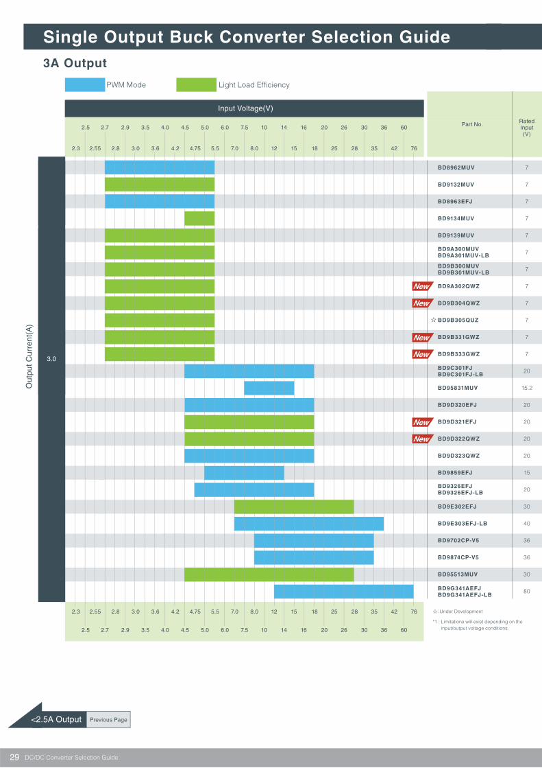
Single Output Buck Converter Selection Guide
2.5 2.7 2.9 3.5 4.0 4.5 5.0 6.0 7.5 10 14 16 20 26 30 36 60
2.3 2.55 2.8 3.0 3.6 4.2 4.75 5.5 7.0 8.0 12 15 18 25 28 35 42 76
2.5 2.7 2.9 3.5 4.0 4.5 5.0 6.0 7.5 10 14 16 20 26 30 36 60
2.3 2.55 2.8 3.0 3.6 4.2 4.75 5.5 7.0 8.0 12 15 18 25 28 35 42 76
Input Voltage(V)
Out
put C
urre
nt(A
)
7
7
7
7
7
7
7
7
7
7
7
7
20
15.2
20
20
20
20
15
20
30
40
36
36
30
80
3.0
BD8962MUV
BD9132MUV
BD8963EFJ
BD9134MUV
BD9139MUV
BD9A302QWZ
BD9B304QWZ
BD9B305QUZ
BD9B331GWZ
BD9B333GWZ
BD95831MUV
BD9D320EFJ
BD9D321EFJ
BD9D322QWZ
BD9D323QWZ
BD9859EFJ
BD9E302EFJ
BD9E303EFJ-LB
BD9702CP-V5
BD9874CP-V5
BD95513MUV
BD9A300MUVBD9A301MUV-LB
BD9B300MUVBD9B301MUV-LB
BD9C301FJBD9C301FJ-LB
BD9326EFJBD9326EFJ-LB
BD9G341AEFJBD9G341AEFJ-LB
<2.5A Output
3A Output
☆:Under Development
DC/DC Converter Selection Guide
RatedInput(V)
Part No.
PWM Mode Light Load Efficiency
Previous Page
*1 : Limitations will exist depending on the input/output voltage conditions.
30
Functions
3
3
3
3
3
3
3
3
3
3
3
3
3
3
3
3
3
3
3
3
3
3
3
3
3
3
0.8 to 2.5 *1
0.8 to 3.3 *1
1.0 to 2.5 *1
3.3
0.8 to 3.3 *1
0.8 to (VIN×0.7)
0.8 to (VIN×0.8)
0.8 to (VIN×0.7)
0.8 to (VIN×0.8)
0.6 to (VIN×0.8)
0.6 to (VIN×0.8)
0.6 to (VIN×0.8)
1.0 to (VIN×0.7)
0.9 to (VIN×0.9)
1.0 to (VIN-3.0)
1.0 to (0.8×(VIN-IO×RON)
0.7 to 5.0
1.0 to VIN *1
1
1
1
1
1
1
1 or 2
1
1 or 2
1
1.3
1.3
0.5
0.5 to 0.8
0.7
0.7
0.7
0.7
0.75
0.38
0.55
0.3
0.11
0.11
0.2 to 1.0
0.05 to 0.75
Current
Current
Current
Current
Current
Current
ON time
Current
ON time
ON time
ON time
ON time
Current
ON time
ON time
ON time
ON time
ON time
Current
Current
Current
Current
Voltage
Voltage
ON time
Current
Latch
Latch
Latch
Latch
Latch
Recovery
Recovery
Recovery
Recovery
Recovery
Latch
Recovery
Latch
Latch
Recovery
Recovery
Recovery
Recovery
Recovery
Recovery
Recovery
Recovery
Recovery
Recovery
Latch
Recovery
Latch
Latch
Latch
Latch
Latch
Recovery
Recovery
Recovery
Recovery
Recovery
Recovery
Recovery
Recovery
Recovery
Recovery
Recovery
Recovery
Recovery
Recovery
Recovery
Recovery
Recovery
Recovery
Recovery
Recovery
Recovery
Output Discharge
Output Discharge
VQFN020V4040
VQFN020V4040
HTSOP-J8
VQFN020V4040
VQFN016V3030
VQFN016V3030
VQFN016V3030
UMMP008AZ020
UMMP008AZ020
SOP-J8
VQFN016V3030
HTSOP-J8
HTSOP-J8
HTSOP-J8
HTSOP-J8
HTSOP-J8
HTSOP-J8
TO220CP-V5
TO220CP-V5
VQFN032V5050
HTSOP-J8
2.7
2.7
2.7
4.5
2.7
2.7
2.7
2.7
2.7
2.7
2.7
2.7
4.5
7.5
4.5
4.5
4.5
4.5
5
4.75
7
7
8
8
4.5
12
5.5
5.5
5.5
5.5
5.5
5.5
5.5
5.5
5.5
5.5
5.5
5.5
18
15
18
18
18
18
14
18
28
36
35
35
28
76
to
to
to
to
to
to
to
to
to
to
to
to
to
to
to
to
to
to
to
to
to
to
to
to
to
to
(VIN×0.125) to (VIN×0.7)(VIN×0.125)≧0.8
0.8 to (VIN×0.5)(VIN×0.5)≦5.5
0.765 to 7.0(VIN×0.07) to (VIN×0.65)
0.765 to 7.0(VIN×0.07) to (VIN×0.65)
0.765 to 7.0(VIN×0.07) to (VIN×0.65)
0.765 to 7.0(VIN×0.07) to (VIN×0.65)
(VIN×0.143) to (VIN×0.7)(VIN×0.143)≧1.0
(VIN×0.06) to (VIN×0.8)(VIN×0.06)≧1.0
VMMP08LZ2020(2.0×2.0×0.4)
UCSP30L1(1.98×1.8×0.33)
UCSP35L1(1.98×1.8×0.4)
UMMP008Z2020(2.0×2.0×0.4)
UMMP008Z2020(2.0×2.0×0.4)
>3.5A Output
DC/DC Converter Selection Guide
Pow
er G
oo
d
Ext
erna
lS
ynch
ron
izat
ion
Var
iabl
e S
oft S
tart
Syn
chro
no
us
Re
ctifi
catio
n
Lig
ht L
oad
Eff
icie
ncy
Ove
r Cur
rent
Pro
tect
ion
The
rmal
Shu
tdow
n
Ove
r Vol
tage
Pro
tect
ion
OutputCurrent
(A)
Input Voltage(V)
SwitchingFrequency
(MHz)
ControlMethod
Other Functions
-40 to +105
-40 to +105
-25 to +85
-40 to +105
-40 to +105
-40 to +85
-40 to +85
-40 to +85
-40 to +85
-40 to +85
-20 to +100
-40 to +85
-40 to +85
-40 to +85
-40 to +85
-40 to +85
-40 to +85
-40 to +85
-40 to +150
-40 to +85
-40 to +85
-10 to +100
-40 to +85
-40 to +85
-40 to +125
-40 to +85
-40 to +125
-40 to +85
-40 to +125
OperatingTemperature
(℃)
Package(mm)
Output Voltage(V)
Next Page
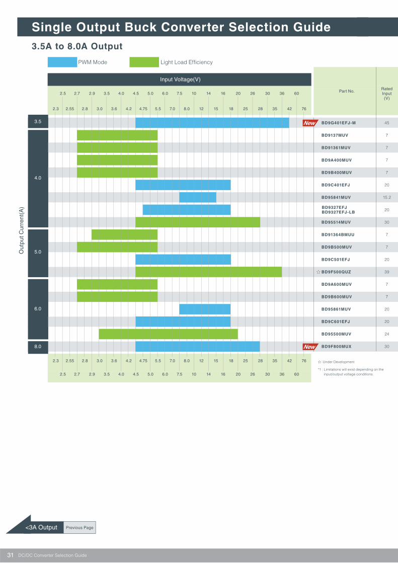
31
Single Output Buck Converter Selection Guide
2.5 2.7 2.9 3.5 4.0 4.5 5.0 6.0 7.5 10 14 16 20 26 30 36 60
2.3 2.55 2.8 3.0 3.6 4.2 4.75 5.5 7.0 8.0 12 15 18 25 28 35 42 76
2.5 2.7 2.9 3.5 4.0 4.5 5.0 6.0 7.5 10 14 16 20 26 30 36 60
2.3 2.55 2.8 3.0 3.6 4.2 4.75 5.5 7.0 8.0 12 15 18 25 28 35 42 76
Input Voltage(V)
Out
put C
urre
nt(A
)
BD9G401EFJ-M
BD9137MUV
BD91361MUV
BD9A400MUV
BD9B400MUV
BD9C401EFJ
BD95841MUV
BD95514MUV
BD91364BMUU
BD9B500MUV
BD9C501EFJ
BD9F500QUZ
BD9A600MUV
BD9B600MUV
BD95861MUV
BD9C601EFJ
BD95500MUV
BD9F800MUX
45
7
7
7
7
20
15.2
20
30
7
7
20
39
7
7
20
20
24
30
3.5
4.0
5.0
6.0
8.0
BD9327EFJBD9327EFJ-LB
<3A Output
3.5A to 8.0A Output
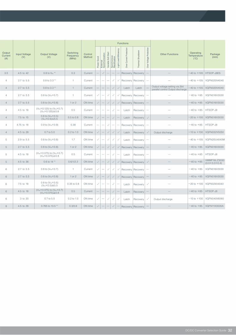
DC/DC Converter Selection Guide
RatedInput(V)
Part No.
PWM Mode Light Load Efficiency
Previous Page
☆:Under Development
*1 : Limitations will exist depending on the input/output voltage conditions.
32
Functions
3.5
4
4
4
4
4
4
4
4
5
5
5
5
6
6
6
6
6
8
0.8 to VIN *1
0.8 to 3.3 *1
0.8 to 3.3 *1
0.8 to (VIN×0.7)
0.8 to (VIN×0.8)
0.9 to (VIN×0.9)
0.7 to 5.0
0.8 to (VIN×0.8)
0.8 to (VIN×0.8)
0.6 to 14 *1
0.8 to (VIN×0.7)
0.8 to (VIN×0.8)
0.7 to 5.0
0.765 to 13.5 *1
0.3
1
1
1
1 or 2
0.5
0.5 to 0.8
0.38
0.2 to 1.0
1.7
1 or 2
0.5
0.6/1/2.2
1
1 or 2
0.35 to 0.8
0.5
0.2 to 1.0
0.3/0.6
Current
Current
Current
Current
ON time
Current
ON time
Current
ON time
ON time
ON time
Current
ON time
Current
ON time
ON time
Current
ON time
ON time
Recovery
Recovery
Latch
Recovery
Recovery
Latch
Latch
Recovery
Latch
Latch
Recovery
Latch
Recovery
Recovery
Recovery
Latch
Latch
Latch
Recovery
Recovery
Recovery
Latch
Recovery
Recovery
Recovery
Recovery
Recovery
Recovery
Recovery
Recovery
Recovery
Recovery
Recovery
Recovery
Recovery
Recovery
Recovery
Recovery
-40 to +105
-40 to +105
-40 to +105
-40 to +85
-40 to +85
-40 to +85
-20 to +100
-40 to +85
-10 to +100
-40 to +105
-40 to +85
-40 to +85
-40 to +85
-40 to +85
-40 to +85
-20 to +100
-40 to +85
-10 to +100
-40 to +85
4.5
2.7
2.7
2.7
2.7
4.5
7.5
4.75
4.5
2.9
2.7
4.5
4.5
2.7
2.7
7.5
4.5
3
4.5
42
5.5
5.5
5.5
5.5
18
15
18
28
5.5
5.5
18
36
5.5
5.5
18
18
20
28
to
to
to
to
to
to
to
to
to
to
to
to
to
to
to
to
to
to
to
(VIN×0.125) to (VIN×0.7)(VIN×0.125)≧0.8
0.8 to (VIN×0.5)(VIN×0.5)≦5.5
(VIN×0.075) to (VIN×0.7)(VIN×0.075)≧0.8
0.8 to (VIN×0.5)(VIN×0.5)≦5.5
(VIN×0.075) to (VIN×0.7)(VIN×0.075)≧0.8
Output discharge
Output discharge
Output voltage setting via 2bit parallel control Output discharge
HTSOP-J8ES
VQFN020V4040
VQFN020V4040
VQFN016V3030
VQFN016V3030
HTSOP-J8
VQFN016V3030
HTSOP-J8
VQFN032V5050
VQFN20U4040M
VQFN016V3030
HTSOP-J8
VQFN016V3030
VQFN016V3030
VQFN024V4040
HTSOP-J8
VQFN040V6060
VQFN11X3535A
VMMP16LZ3030(3.0×3.0×0.4)
DC/DC Converter Selection Guide
Pow
er G
oo
d
Ext
erna
lS
ynch
ron
izat
ion
Var
iabl
e S
oft S
tart
Syn
chro
no
us
Re
ctifi
catio
n
Lig
ht L
oad
Eff
icie
ncy
Ove
r Cur
rent
Pro
tect
ion
The
rmal
Shu
tdow
n
Ove
r Vol
tage
Pro
tect
ion
OutputCurrent
(A)
Input Voltage(V)
SwitchingFrequency
(MHz)
ControlMethod
Other Functions OperatingTemperature
(℃)
Package(mm)
Output Voltage(V)
33
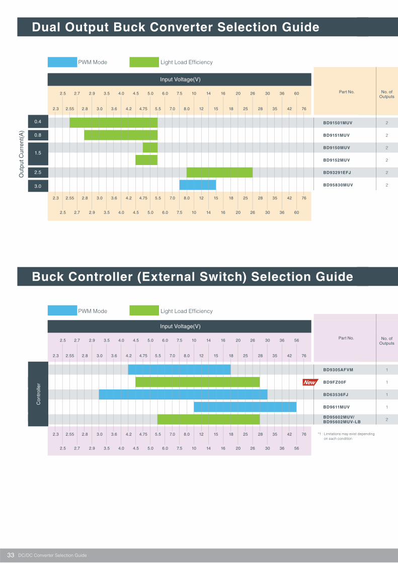
Dual Output Buck Converter Selection GuideO
utpu
t Cur
rent
(A)
2.5 2.7 2.9 3.5 4.0 4.5 5.0 6.0 7.5 10 14 16 20 26 30 36 60
2.5 2.7 2.9 3.5 4.0 4.5 5.0 6.0 7.5 10 14 16 20 26 30 36 60
2.3 2.55 2.8 3.0 3.6 4.2 4.75 5.5 7.0 8.0 12 15 18 25 28 35 42 76
2.3 2.55 2.8 3.0 3.6 4.2 4.75 5.5 7.0 8.0 12 15 18 25 28 35 42 76
Input Voltage(V)
BD91501MUV
BD9151MUV
BD9150MUV
BD9152MUV
BD93291EFJ
BD95830MUV
No. ofOutputs
2
2
2
2
2
2
0.4
0.8
1.5
2.5
3.0
2.5 2.7 2.9 3.5 4.0 4.5 5.0 6.0 7.5 10 14 16 20 26 30 36 56
2.5 2.7 2.9 3.5 4.0 4.5 5.0 6.0 7.5 10 14 16 20 26 30 36 56
2.3 2.55 2.8 3.0 3.6 4.2 4.75 5.5 7.0 8.0 12 15 18 25 28 35 42 76
2.3 2.55 2.8 3.0 3.6 4.2 4.75 5.5 7.0 8.0 12 15 18 25 28 35 42 76
Input Voltage(V)
BD9305AFVM
BD9FZ00F
BD63536FJ
BD9611MUV
BD95602MUV/BD95602MUV-LB
1
1
1
1
2
Con
trol
ler
Buck Controller (External Switch) Selection Guide
*1 : Limitations may exist depending on each condition
DC/DC Converter Selection Guide
Part No.
PWM Mode Light Load Efficiency
PWM Mode Light Load Efficiency
Part No. No. ofOutputs
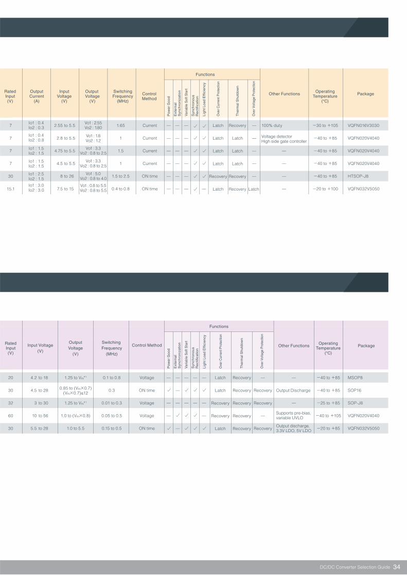
34
Functions
7
7
7
7
30
15.1
1.65
1
1.5
1
1.5 to 2.5
0.4 to 0.8
Current
Current
Current
Current
ON time
ON time
Latch
Latch
Latch
Latch
Recovery
Latch
Recovery
Latch
Latch
Latch
Recovery
Recovery
100% duty
Voltage detectorHigh side gate controller
-30 to +105
-40 to +85
-40 to +85
-40 to +85
-40 to +85
-20 to +100
VQFN016V3030
VQFN020V4040
VQFN020V4040
VQFN020V4040
HTSOP-J8
VQFN032V5050
Io1 : 0.4Io2 : 0.3
Vo1 : 2.55Vo2 : 1.80
Vo1 : 1.8Vo2 : 1.2
Vo1 : 3.3Vo2 : 0.8 to 2.5
Vo1 : 3.3Vo2 : 0.8 to 2.5
Vo1 : 5.0Vo2 : 0.8 to 4.0
Vo1 : 0.8 to 5.5Vo2 : 0.8 to 5.5
Io1 : 0.4Io2 : 0.8
Io1 : 1.5Io2 : 1.5
Io1 : 1.5Io2 : 1.5
Io1 : 2.5Io2 : 1.5
Io1 : 3.0Io2 : 3.0
2.55
2.8
4.75
4.5
8
7.5
5.5
5.5
5.5
5.5
26
15
to
to
to
to
to
to
Functions
20
30
32
60
30
0.1 to 0.8
0.3
0.01 to 0.3
0.05 to 0.5
0.15 to 0.5
1.25 to VIN*1
1.25 to VIN*1
1.0 to (VIN×0.8)
1.0 to 5.5
Voltage
ON time
Voltage
Voltage
ON time
Recovery
Recovery
Recovery
Latch
Latch
Recovery
Recovery
Latch
Recovery
Recovery
Recovery
Recovery
Recovery
Output Discharge
Supports pre-bias,variable UVLO
Output discharge,3.3V LDO, 5V LDO
-40 to +85
-40 to +85
-25 to +85
-40 to +105
-20 to +85
MSOP8
SOP16
SOP-J8
VQFN020V4040
VQFN032V5050
0.85 to (VIN×0.7)(VIN×0.7)≤12
4.2
4.5
3
10
5.5
18
28
30
56
28
to
to
to
to
to
Latch
DC/DC Converter Selection Guide
Pow
er G
oo
d
Ext
erna
lS
ynch
ron
izat
ion
Var
iabl
e S
oft S
tart
Syn
chro
no
us
Re
ctifi
catio
n
Lig
ht L
oad
Eff
icie
ncy
Ove
r Cur
rent
Pro
tect
ion
The
rmal
Shu
tdow
n
Pow
er G
oo
d
Ext
erna
lS
ynch
ron
izat
ion
Var
iabl
e S
oft S
tart
Syn
chro
no
us
Re
ctifi
catio
n
Lig
ht L
oad
Eff
icie
ncy
Ove
r Cur
rent
Pro
tect
ion
The
rmal
Shu
tdow
n
Ove
r Vol
tage
Pro
tect
ion
RatedInput(V)
OutputCurrent
(A)
InputVoltage
(V)
SwitchingFrequency
(MHz)
ControlMethod
Other Functions OperatingTemperature
(℃)
PackageOutput Voltage
(V)
Other Functions PackageRatedInput(V)
Switching Frequency
(MHz)
OutputVoltage
(V)
Control Method OperatingTemperature
(℃)
Input Voltage(V)
Ove
r Vol
tage
Pro
tect
ion
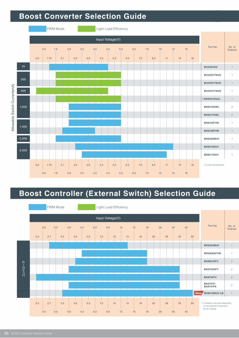
35
Boost Converter Selection GuideA
llow
able
Sw
itch
Cur
rent
(mA
)
10
300
500
1,000
1,400
2,000
2,500
0.9 1.8 2.8 3.5 4.0 4.5 5.5 6.5 7.5 10 12 16
0.9 1.8 2.8 3.5 4.0 4.5 5.5 6.5 7.5 10 12 16
0.6 1.75 2.1 3.0 3.6 4.2 5.0 6.0 7.0 8.0 11 15 18
0.6 1.75 2.1 3.0 3.6 4.2 5.0 6.0 7.0 8.0 11 15 18
BU33DV5G
BU33DV7NUX
BU34DV7NUX
BU33UV7NUX
BD83070GUL
BD8316GWL
BD8317GWL
BD8152FVM
BD8158FVM
BD8306MUV
BD8314NUV
BD8311NUV
1
1
1
1
1
2
2
1
1
1
1
1
Boost Controller (External Switch) Selection Guide
2.6 3.0 3.6 4.2 6.0 8.0 12 15 18 26 30 42
2.6 3.0 3.6 4.2 6.0 8.0 12 15 18 26 30 42
2.5 2.7 3.5 4.0 5.0 7.0 10 14 16 20 28 35 60
2.5 2.7 3.5 4.0 5.0 7.0 10 14 16 20 28 35 60
BD8303MUV
BD9306AFVM
BD9851EFV
BA9743AFV
BA9744FV
BD9615MUV-LB
1
1
2
2
2
2
1
コントローラ
BA9741F/BA9741FS
Input Voltage(V)
Input Voltage(V)
☆:Under Development
*1: Limitations may exist depending on the external components and IC settings
DC/DC Converter Selection Guide
PWM Mode Light Load Efficiency
PWM Mode Light Load Efficiency
Part No. No. ofOutputs
Part No. No. ofOutputs
36
Current
Current
Current
Current
Current
Current
Current
Current
Current
Voltage
Voltage
Voltage
-40 to +85
-40 to +85
-40 to +85
-40 to +85
-40 to +85
-35 to +85
-35 to +85
-40 to +85
-40 to +125
-40 to +85
-25 to +85
-25 to +85
SSOP5
VSON010V3030
VSON010V3030
VSON010X3020
UCSP50L1C(1.2×1.6)
UCSP50L1(1.8×1.5)
UCSP50L1(1.8×1.5)
MSOP8
MSOP8
VQFN016V3030
VSON010V3030
VSON010V3030
1.75
1.8
1.8
0.6
1.8
2.5
2.5
2.5
2.1
1.8
3
3.5
4.5
5.5
5.5
4.5
5.5
5.5
5.5
5.5
4
5.5
12
11
to
to
to
to
to
to
to
to
to
to
to
to
10
300
300
500
1,000
1,000
1,000
1,400
1,400
2,000
2,500
2,500
3.3
3.3
3.4
3.3
3.3
VIN to 14
VIN to 14
1.8 to 5.2
4.0 to 12
4.0 to 11
100
600
600
800
1500
1600
800
600/1,200
600/1,200
300 to 2,000
1,200
1,200
Vo1 : -9.0 to -1.0Vo2 : VIN to 18
Vo1 : -9.0 to -1.0Vo2 : VIN to 18
Functions
Bo
ost
Bu
ck-B
oo
st
SE
PIC
Inve
rtin
g
Syn
chro
no
us
Re
ctifi
catio
n
Ligh
t Loa
d E
ffici
ency
Sof
t Sta
rt
Inpu
t Pas
s-T
hrou
gh
UV
LO
Ove
rcur
rent
Pro
tect
ion
Variable
Variable
Recovery
Recovery
Recovery
Recovery
Recovery
Latch
Latch
Recovery
Recovery
Latch
Latch
Latch
The
rmal
Shu
tdow
n
Voltage
Voltage
Voltage
Voltage
Voltage
Voltage
Voltage
-25 to +85
-40 to +85
-40 to +85
-40 to +85
-40 to +85
-40 to +85
-40 to +105
2.7
4.2
4
3.6
2.5
3.6
3.5
14
18
18
35
35
35
60
to
to
to
to
to
to
to
15
20
20
36
36
36
62
1.8 to 12
VIN to (VIN/0.3)
1.0 or more *1
2.505 or more *1
1.222 or more *1
2.5 or more *1
VIN to (VIN/0.2)
200 to 1,000
100 to 800
10 to 3,000
10 to 800
10 to 800
10 to 800
100 to 2,500
Functions
Latch
Latch
Latch
Latch
Latch
Latch
Recovery
Recovery
Recovery
Recovery
Recovery
Recovery
Recovery
Recovery
VQFN016V3030
MSOP8
HTSSOP-B20
SSOP-B16
SSOP-B16
VQFN16KV3030
SOP16/SSOP-A16
External synchronizationPower Good
DC/DC Converter Selection Guide
ControlMethod
OperatingTemperature
(℃)
Package(mm)
AllowableSwitchCurrent
(mA)
Input Voltage(V)
Output Voltage(V)
SwitchingFrequency
(kHz)
ControlMethod
OperatingTemperature
(℃)
Other Functions PackageRated Input(V)
Input Voltage(V)
OutputVoltage
(V)
SwitchingFrequency
(kHz)
Bo
ost
Bu
ck-B
oo
st
Inve
rtin
g
Bu
ck
Ena
ble
Var
iabl
e S
oft S
tart
Syn
chro
no
us
Re
ctifi
catio
n
The
rmal
Shu
tdow
n
Sho
rt-C
ircu
itP
rote
ctio
n
Dead timeadjustment
Dead timeadjustment
Dead timeadjustment
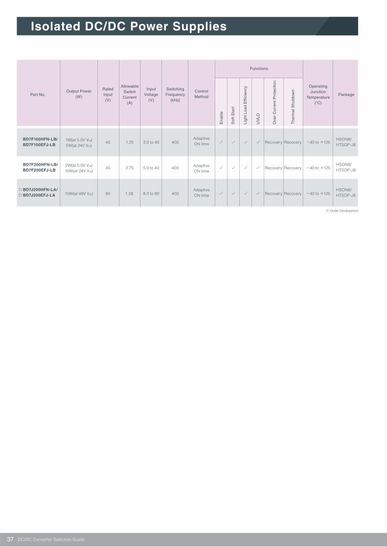
37
Isolated DC/DC Power Supplies
BD7F100HFN-LB/
BD7F100EFJ-LB
BD7F200HFN-LB/
BD7F200EFJ-LB
BD7J200HFN-LA/
BD7J200EFJ-LA
1W(at 5.0V VIN)5W(at 24V VIN)
2W(at 5.0V VIN)10W(at 24V VIN)
10W(at 48V VIN)
45
45
80
1.25
2.75
1.38
3.0 to 40
5.0 to 40
8.0 to 80
400
400
400
-40 to +125
-40 to +125
-40 to +125
Functions
AdaptiveON time
AdaptiveON time
AdaptiveON time
HSON8/HTSOP-J8
HSON8/HTSOP-J8
HSON8/HTSOP-J8
Recovery
Recovery
Recovery
Recovery
Recovery
Recovery
☆:Under Development
DC/DC Converter Selection Guide
Part No.Output Power
(W)
RatedInput(V)
AllowableSwitchCurrent
(A)
InputVoltage
(V)
SwitchingFrequency
(kHz)
OperatingJunction
Temperature(℃)
PackageControlMethod
Ena
ble
Sof
t Sta
rt
Lig
ht L
oad
Eff
icie
ncy
UV
LO
Ove
r C
urre
nt P
rote
ctio
n
The
rmal
Shu
tdow
n
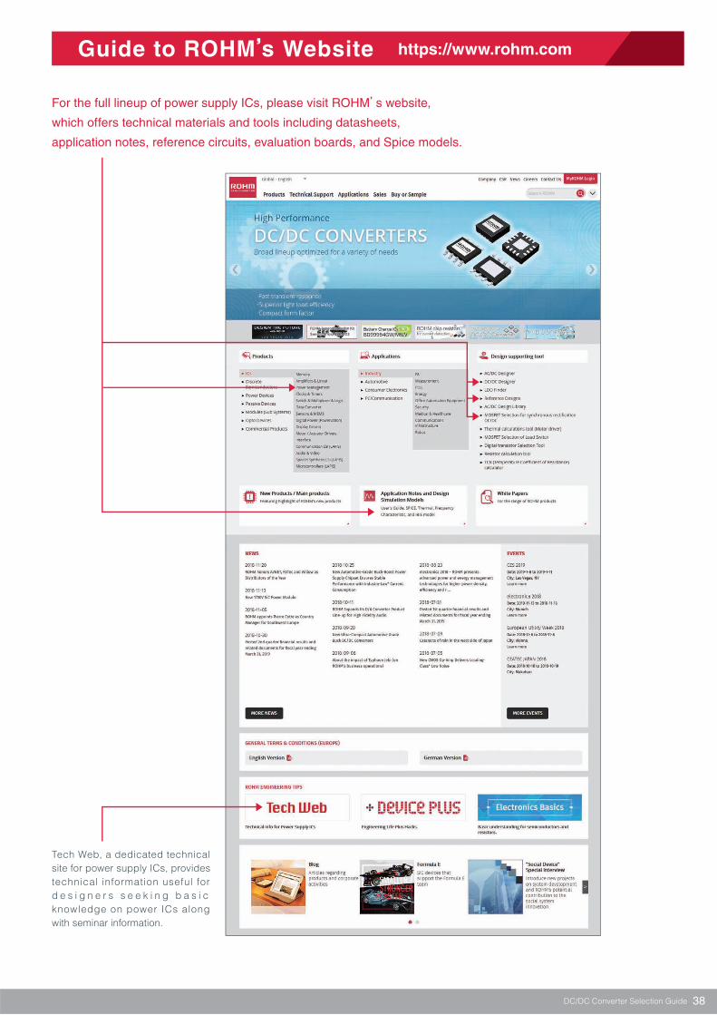
38
Guide to ROHM’s Website https://www.rohm.com
For the full lineup of power supply ICs, please visit ROHM’s website,
which offers technical materials and tools including datasheets,
application notes, reference circuits, evaluation boards, and Spice models.
Tech Web, a dedicated technical site for power supply ICs, provides technical information useful for d e s i g n e r s s e e k i n g b a s i c knowledge on power ICs along with seminar information.
DC/DC Converter Selection Guide
No.61P7169E 02.2019 PDF
2018October 1st