Embed Size (px)
Citation preview
NTUEE Electronics – L.H. Lu 8-1
CHAPTER 8 DIFFERENTIAL AND MULTISTAGE AMPLIFIERS
Chapter Outline8.1 The CMOS Differential Pair8.2 Small-Signal Operations of the MOS Differential Pair8.3 The BJT Differential Pair8.4 Other Non-ideal Characteristics of the Differential Amplifier8.5 The Differential Amplifier with Active Load

NTUEE Electronics – L.H. Lu 8-2
8.1 The MOS Differential Pair
The differential pair (differential amplifier) configurationWidely used building block in analog integrated circuit design Performance depends critically on the matching of the devices Utilizes more components than single-ended circuits Well suited for IC fabrication
Advantages of using differential pair Less sensitive to noise and interference than single-ended circuits Bias is provided without the need for bypass and coupling capacitors
The CMOS differential pairThe design philosophy for ICs is different from that of discrete-component circuits Two matched transistors are used Identical device parameters for Q1 and Q2
(kn, Vt, and even layout) The source terminals are connected together Biased by a constant-current source Resistive loads are used for illustration Differential input at the gate terminals Differential output at the drain terminals

NTUEE Electronics – L.H. Lu 8-3
𝐼
2=
1
2𝑘
𝑊
𝐿(𝑉 − 𝑉 )
𝑉 = 𝑉 − 𝑉 = 𝑉 −𝐼
𝑘 (𝑊/𝐿)− 𝑉
𝑉 =𝐼
𝑘 (𝑊/𝐿)
𝑉 = 𝑉 = 𝑉 −𝐼
2𝑅
Operation with a common-mode input voltageCircuit analysis Both inputs are connected to a common-mode voltage VCM
The differential pair Q1 and Q2 are in saturation The current divides equally due to device matching
Output does not respond to VCM
VOV is defined at ID1 = ID2 = I/2Input common-mode range (ICMR): The range of VCM for proper operation Both Q1 and Q2 should be in saturationVCM,max = VDD–RDI/2+Vt
VCM,min = -VSS+VCS(headroom for current source)+VGS

NTUEE Electronics – L.H. Lu 8-4
Operation with a differential input voltageA difference voltage vid exists between the input terminalsThe current of Q1 is different from that of Q2 as vGS1 vGS2
The overall current I remains unchangedThe value of vid at which the entire bias current I is steered into Q1 is
The current I can be steered from one transistor to the other by varying vid in the range
Differential pair as a linear amplifier Keep the differential input voltage vid small The currents of the transistor pair become I/2 I I is linearly proportional to vid for small-signal operation A differential output voltage is taken between the two drains as 2IRD
𝑣 = 𝑉 +2𝐼
𝑘 (𝑊/𝐿)= 𝑉 + 2𝑉
𝑣 = 𝑉
𝑣 , = 2𝑉
− 2𝑉 < 𝑣 < 2𝑉

Large-signal operation
Drain currents of the differential pair
Normalized transfer characteristics Nonlinear transfer characteristics The overdrive voltage VOV is calculated as
iD1 = iD2 = I /2Small-signal approximation Linear I-V characteristics for small vid
Transconductance: Gm iD/vid = I/VOV
NTUEE Electronics – L.H. Lu 8-5
𝑣 = 𝑣 − 𝑣 =2𝑖
𝑘 (𝑊/𝐿)−
2𝑖
𝑘 (𝑊/𝐿)
𝐼 = 𝑖 + 𝑖
𝑖 =𝐼
2+
𝐼
𝑉
𝑣
21 −
𝑣
2𝑉
𝑖 =𝐼
2−
𝐼
𝑉
𝑣
21 −
𝑣
2𝑉
𝑖 ≈𝐼
2+
𝐼
𝑉
𝑣
2
𝑖 ≈𝐼
2−
𝐼
𝑉
𝑣
2

Linearity of the differential pairThe linearity of the differential pair can be increased by increasing the overdrive voltage VOV
Linearity-transconductance trade-off: Smaller aspect ratio (W/L) of Q1 and Q2 at fixed bias current I Resulting in smaller transconductance and smaller gain
Linearity-power trand-off: Larger bias current I with fixed aspect ratio Resulting in larger transconductance and gain at the cost of higher power dissipation
NTUEE Electronics – L.H. Lu 8-6
8.2 Small-Signal Operation of the MOS Differential Pair
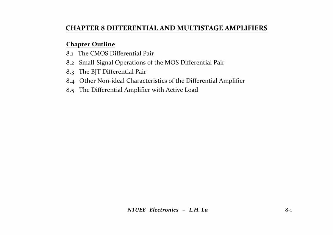
Small-signal analysis technique for differential amplifiersThe ac inputs are defined as vg1 and vg2 at the differential pair based on the small-signal modelIt can also be treated as superposition of differential (vid) and common-mode (vicm) voltagesThe circuit analysis can be divided into differential and common-mode operations
Differential gainThe differential input signal (vid) is applied in a complementary (or balanced) mannerSingle-ended outputs (vo1 and vo2): output taken between one of the drains and groundDifferential output (vod): output taken between the two drainsDifferential gain is defined as the ratio of vod to vid:
NTUEE Electronics – L.H. Lu 8-7
𝐴 ≡𝑣
𝑣=
𝑣 − 𝑣
𝑣 − 𝑣
VCM + vg1 VCM + vg1
VD + vo1 VD + vo1
vg1 vg2
ac equivalent circuit
vo1 vo1
𝑣 = 𝑣 − 𝑣
𝑣 =𝑣 + 𝑣
2

Small-signal circuit analysis (simplified model):
Differential gain:
Small-signal circuit analysis (with ro and RSS):
Differential gain:
NTUEE Electronics – L.H. Lu 8-8
𝑖 =𝑣
1/𝑔 + 1/𝑔 =
𝑔 𝑣
2
→ 𝑣 = 0
𝐴 ≡𝑣
𝑣=
𝑣 − 𝑣
𝑣= 𝑔 𝑅
𝑣 = −𝑖𝑅 = −𝑔 𝑅 𝑣
2
𝑣 = 𝑖𝑅 =𝑔 𝑅 𝑣
2
𝑖 =𝑣
1𝑔
+1
𝑔
𝑖 𝑖
𝑣 = 0V
𝑔𝑣
2− 𝑣 +
𝑣 − 𝑣
𝑟+ 𝑔 −
𝑣
2− 𝑣 +
𝑣 − 𝑣
𝑟= 0
𝑔𝑣
2− 𝑣 +
𝑣 − 𝑣
𝑟+
𝑣
𝑅= 0
𝑔 −𝑣
2− 𝑣 +
𝑣 − 𝑣
𝑟+
𝑣
𝑅= 0
→ 𝑣 = 0
𝑣 = −𝑣 =𝑔 /2
1/𝑟 + 1/𝑅𝑣
𝐴 ≡𝑣
𝑣=
𝑣 − 𝑣
𝑣= 𝑔 𝑅 ||𝑟
𝑣
𝑟 𝑟
𝑅

The differential half-circuitVirtual ground: Differential operation for a symmetrical circuit The voltage at the nodes on the symmetrical axis (the joint source connection) must be zero A signal ground is established at the source terminals without a large bypass capacitor
The differential half-circuit analysis: A technique useful to simplify the ac analysis of fully differential circuits All the nodes on symmetric line are considered ac ground The complete circuit can typically be separated into two half-circuits Performance of a symmetrical differential circuit can be evaluated by half-circuit analysis
NTUEE Electronics – L.H. Lu 8-9
𝐴 ≡𝑣
𝑣= 𝑔 (𝑅 ||𝑟 ) ≈ 𝑔 𝑟

The differential amplifier with current-source load
NTUEE Electronics – L.H. Lu 8-10
𝐴 ≡𝑣
𝑣= 𝑔 (𝑟 ||𝑟 )
𝐴 ≡𝑣
𝑣= 𝑔 (𝑅 | 𝑅 ≈ 𝑔 (𝑔 𝑟 𝑟 ||𝑔 𝑟 𝑟 )
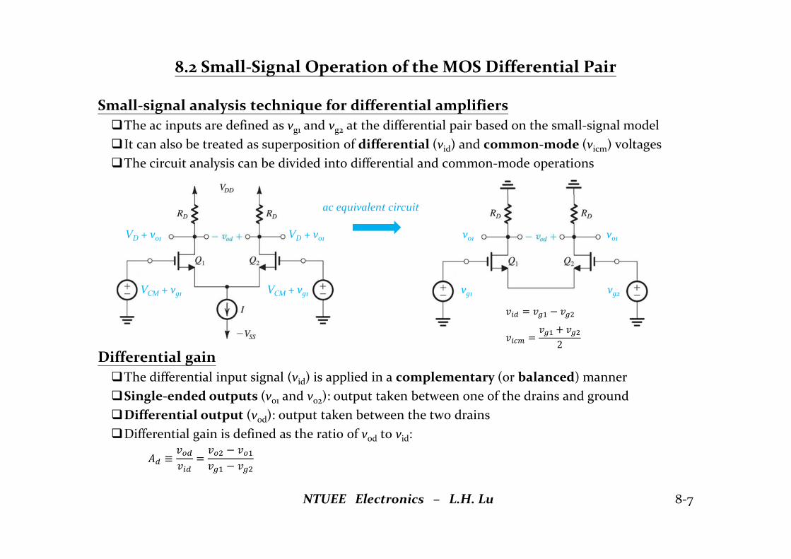
Example for differential half-circuit analysis
NTUEE Electronics – L.H. Lu 8-11
𝐴 ≡𝑣
𝑣=
𝑔
1 + 𝑔 𝑅𝑅 ||
𝑅
2

NTUEE Electronics – L.H. Lu 8-12
Common-mode gain of a differential pairA differential pair with ideal current source The output resistance (RSS) is infinite Drain currents of Q1 and Q2 do not change with the input
common-mode voltage VCM
The single-ended outputs remain unchanged The differential output voltage and common-mode gain are zero
A differential pair with a practical current source The output resistance (RSS) is finite Drain currents of Q1 and Q2 change simultaneously with VCM
The singled-ended outputs vary with VCM
The differential output voltage and common-mode gain are zeroThe differential pair rejects common-mode signals regardless the
value of RSS, resulting in zero differential output voltage
𝑣 = 𝑖1
𝑔+ 2𝑖𝑅 → 𝑖 =
𝑣
1𝑔
+ 2𝑅
𝑣 = 𝑣 = −𝑅
1𝑔
+ 2𝑅𝑣 ≈ −
𝑅
2𝑅𝑣
𝑣 = 𝑣 − 𝑣 = 0

Common-mode half-circuitThe common-mode half-circuit analysis: Circuit analysis technique for symmetrical circuit with common-mode operation The symmetrical points are equal potential No current flowing across the symmetrical line and can be treated as open The complete circuit can be typically divided into two half-circuits The performance can be evaluated by common-mode half-circuit to simplify the analysis
NTUEE Electronics – L.H. Lu 8-13
𝑣 = 𝑣 = −𝑔 𝑅
1 + 2𝑔 𝑅𝑣 ≈ −
𝑅
2𝑅𝑣

Complete small-signal analysis:
Overall response:
NTUEE Electronics – L.H. Lu 8-14
vg1 vg2
RSS
𝑣 = 𝑣 − 𝑣
AC equivalent circuit:
𝑣 =𝑣 + 𝑣
2
Differential operation:
RSS
𝑣
2−
𝑣
2
𝑣 = −𝑔 𝑅 𝑣
2
𝑣 =𝑔 𝑅 𝑣
2
𝐴 =𝑣 − 𝑣
𝑣= 𝑔 𝑅
Common-mode operation:
RSS
𝑣 𝑣
𝐴 =𝑣 − 𝑣
𝑣= 0
𝑣 ≈ −𝑅
2𝑅𝑣
𝑣 ≈ −𝑅
2𝑅𝑣
𝑣 = 𝑉 _ −𝑔 𝑅
2𝑣 −
𝑅
2𝑅𝑣
𝑣 = 𝑉 _ +𝑔 𝑅
2𝑣 −
𝑅
2𝑅𝑣

Device mismatch in the differential pairMismatch between Q1 and Q2 or RD1 and RD2 leads to non-ideal effectsAssume RD1 = RD+RD and RD2 = RD for resistance mismatchOperation with a differential input voltage vid:
The mismatch is generally small in modern integrated circuit technology The differential gain Ad does not change significantly due to mismatch Analysis of device mismatch is typically focused on non-ideal effects in common-mode operation
NTUEE Electronics – L.H. Lu 8-15
𝑣
2=
1
𝑔𝑖 + 𝑅 (𝑖 + 𝑖 )
−𝑣
2=
1
𝑔𝑖 + 𝑅 (𝑖 + 𝑖 )
→ 𝑖 = −𝑖 = 𝑔𝑣
2
→ 𝑣 = 𝑣 − 𝑣 = 𝑔 𝑅 1 +∆𝑅
2𝑅𝑣
→ 𝐴 = 𝑔 𝑅 1 +∆𝑅
2𝑅≈ 𝑔 𝑅
∆𝑅 /𝑅
i1+i2
i1 i2vid/2 -vid/2
RD+RD RD
Q1 Q2

Effect of resistance mismatchCommon-mode gain:
For a current source with finite RSS, mismatch in RD causes a finite common-mode gain Acm
Common-mode rejection ratio (CMRR): CMRR is defined as the ratio of differential-mode gain and the common-mode gain A measure of the effectiveness of the differential pair in rejecting common-mode interference Is given by CMRR = |Ad/Acm| and usually expressed in decibels CMRR (dB) = 20log|Ad/Acm|
CMRR of the differential amplifier with respect to the resistance mismatch
Utilizes a bias current source with a high output resistance
High degree of matching between the drain resistance
NTUEE Electronics – L.H. Lu 8-16
i1+i2
i1 i2vicm vicm
RD+RD RD
Q1 Q2
𝑣 =1
𝑔𝑖 + 𝑅 (𝑖 + 𝑖 ) =
1
𝑔𝑖 + 𝑅 (𝑖 + 𝑖 )
→ 𝑖 = 𝑖 =𝑣
1𝑔
+ 2𝑅
→ 𝑣 = 𝑣 − 𝑣 =𝑅
1𝑔
+ 2𝑅
∆𝑅
𝑅𝑣
→ 𝐴 ≡𝑣
𝑣≈
𝑅
2𝑅
∆𝑅
𝑅
C𝑀𝑅𝑅 =𝐴
𝐴=
2𝑔 𝑅
∆𝑅 /𝑅

Effect of transconductance mismatchMismatch exists between Q1 and Q2
Common-mode gain:
Common-mode rejection ratio:
NTUEE Electronics – L.H. Lu 8-17
i1+i2
i1 i2vicm vicm
RD RD
Q1 Q2
𝑔 = 𝑔 +∆𝑔
2
𝑔 = 𝑔 −∆𝑔
2
→ 𝐴 ≡𝑣
𝑣≈
𝑅
2𝑅
∆𝑔
𝑔
𝑣 =1
𝑔𝑖 + 𝑅 𝑖 + 𝑖 =
1
𝑔𝑖 + 𝑅 𝑖 + 𝑖
𝑣 = −𝑖 𝑅 = −𝑔 𝑅
1 + 𝑔 + 𝑔 𝑅𝑣
𝑣 = −𝑖 𝑅 = −𝑔 𝑅
1 + 𝑔 + 𝑔 𝑅𝑣
→ 𝑣 = 𝑣 − 𝑣 =∆𝑔 𝑅
1 + 2𝑔 𝑅𝑣
𝐶𝑀𝑅𝑅 ≡𝐴
𝐴≈
2𝑔 𝑅
∆𝑔 /𝑔

8.3 The BJT Differential Pair
Circuit configurationTwo identical BJT transistors Q1 and Q2 with emitters jointed togetherBiased with a current source
Input common-mode rangeAllowable range of VCM for Q1 and Q2 in active mode
Common-mode operationCommon-mode input voltage VCM for vB1 and vB2
Single-ended output voltage:
Differential output voltage:
Finite output resistance of the current source Single-ended output change with VCM
Differential output is still zero
NTUEE Electronics – L.H. Lu 8-18
𝑉 ≈ 𝑉 + 0.5V = 𝑉 − 𝛼𝑅𝐼
2+ 0.5V
𝑉 = −𝑉 + 𝑉 + 𝑉
𝑣 = 𝑉 − 𝛼𝑅 𝐼/2
𝑣 = 𝑉 − 𝛼𝑅 𝐼/2
𝑣 = 𝑣 − 𝑣 = 0

Large-signal operationTransfer characteristics
Normalized characteristics The bias current is divided equally for vid = 0 Unequal current through Q1 and Q2 for vid 0 A relatively small vid for complete current switching The linearity can be improved by emitter degeneration Re
Transconductance and gain decrease due to emitter degeneration
NTUEE Electronics – L.H. Lu 8-19
𝑖
𝑖=
𝐼𝛼
𝑒( )/
𝐼𝛼
𝑒( )/= 𝑒( )/
𝑖 + 𝑖 = 𝐼
𝑖 =𝐼
1 + 𝑒𝑥𝑝(−𝑣 /𝑉 )
𝑖 =𝐼
1 + 𝑒𝑥𝑝(𝑣 /𝑉 )
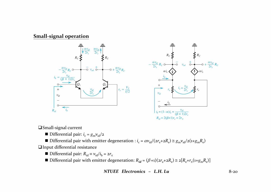
Small-signal operation
Small-signal current Differential pair: ic = gmvid/2 Differential pair with emitter degeneration : ic = vid/(2re+2Re) gmvid/2(1+gmRe)
Input differential resistance Differential pair: Rid vid/ib = 2r Differential pair with emitter degeneration: Rid = (+1)(2re+2Re) 2[Re+r(1+gmRe)]
NTUEE Electronics – L.H. Lu 8-20

Differential gain
Differential pair: Ad vod/vid = gmRC
Differential pair with emitter degeneration: Ad = RC/(re+Re) gmRC/(1+gmRe) The differential amplifier can also be fed in a single-ended fashion
Equivalent circuit model
NTUEE Electronics – L.H. Lu 8-21

Common-mode gain and CMRRDifferential pair with device matching:
Differential pair with resistance mismatch:
High output resistance is desirable for current source Resistance mismatch for the load should be minimized
NTUEE Electronics – L.H. Lu 8-22
𝑣 = 𝑣 = −𝛼𝑅
𝑟 + 2𝑅𝑣
𝑣 = 𝑣 − 𝑣 = 0
RD+RDRD
ie1 ie2
ie1+ie2
ie1 ie2
𝑣 = −𝛼𝑅
𝑟 + 2𝑅𝑣
𝑣 = −𝛼(𝑅 + ∆𝑅 )
𝑟 + 2𝑅𝑣
𝑣 = 𝑣 − 𝑣 = −𝛼∆𝑅
𝑟 + 2𝑅𝑣
𝐴 ≡𝑣
𝑣= −
𝛼∆𝑅
𝑟 + 2𝑅≈ −
𝑅
2𝑅
∆𝑅
𝑅
𝐶𝑀𝑅𝑅 =2𝑔 𝑅
∆𝑅 /𝑅
𝑣 = 𝑖 𝑟 + 𝑖 + 𝑖 𝑅 = 𝑖 𝑟 + (𝑖 + 𝑖 )𝑅
𝑖 = 𝑖 = 𝑣 / 𝑟 + 2𝑅

8.4 Other Non-ideal Characteristics of the Differential Amplifier
Input offset voltage of the MOS differential pairOutput dc offset voltage: the finite output voltage with both input groundedInput offset voltage (VOS): the input referred offset voltage as the output offset divided by gain Output voltage becomes zero if VOS is applied between the inputs Its polarity can not be predetermined
Factors contribute to the dc offset voltage: Mismatch in load resistance RD
Mismatch in aspect ratio (W/L) Mismatch in threshold voltage Vt
NTUEE Electronics – L.H. Lu 8-23

Input offset voltage due to load resistance mismatch
Input offset voltage due to aspect ratio mismatch
Input offset voltage due to threshold voltage mismatch
Input offset voltage: The three mismatch factors are uncorrelated
To minimize the input offset voltageDecrease overdrive voltage VOV
Minimize the device mismatch ratio
NTUEE Electronics – L.H. Lu 8-24
𝑅 = 𝑅 + ∆𝑅 /2
𝑅 = 𝑅 − ∆𝑅 /2𝑉 =
𝑉
𝑔 𝑅=
𝐼
2
∆𝑅
𝑔 𝑅=
𝑉
2
∆𝑅
𝑅
𝑉 =𝑅 (𝐼 − 𝐼 )
𝑔 𝑅=
𝑉
2
∆(𝑊/𝐿)
(𝑊/𝐿)𝑊
𝐿=
𝑊
𝐿−
1
2∆
𝑊
𝐿
𝑊
𝐿=
𝑊
𝐿+
1
2∆
𝑊
𝐿𝐼 =
𝐼
21 +
∆(𝑊/𝐿)
2(𝑊/𝐿)
𝐼 =𝐼
21 −
∆(𝑊/𝐿)
2(𝑊/𝐿)
𝑉 =𝑅 (𝐼 − 𝐼 )
𝑔 𝑅= ∆𝑉
𝑉 = 𝑉 −∆𝑉
2
𝑉 = 𝑉 +∆𝑉
2𝐼 =
𝑘
2𝑉 − 𝑉 1 −
∆𝑉
2(𝑉 − 𝑉 )≈
𝐼
21 −
∆𝑉
𝑉 − 𝑉
𝐼 =𝑘
2𝑉 − 𝑉 1 +
∆𝑉
2(𝑉 − 𝑉 )≈
𝐼
21 +
∆𝑉
𝑉 − 𝑉
𝑉 =𝑉
2
∆𝑅
𝑅+
𝑉
2
∆(𝑊/𝐿)
(𝑊/𝐿)+ ∆𝑉
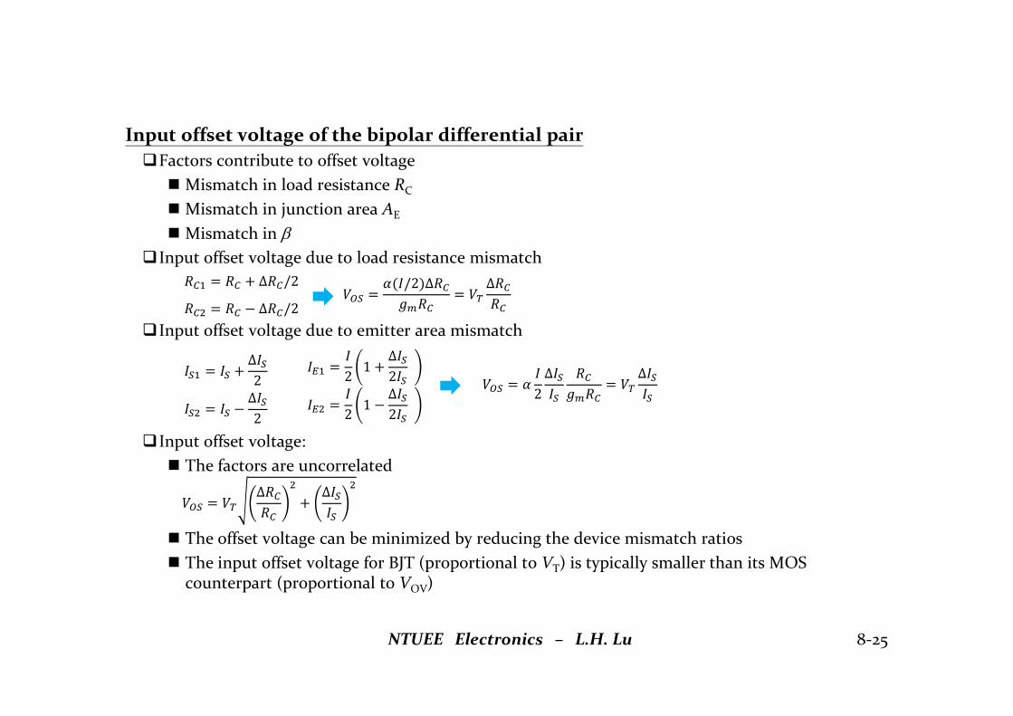
Input offset voltage of the bipolar differential pairFactors contribute to offset voltage Mismatch in load resistance RC
Mismatch in junction area AE
Mismatch in Input offset voltage due to load resistance mismatch
Input offset voltage due to emitter area mismatch
Input offset voltage: The factors are uncorrelated
The offset voltage can be minimized by reducing the device mismatch ratios The input offset voltage for BJT (proportional to VT) is typically smaller than its MOS
counterpart (proportional to VOV)
NTUEE Electronics – L.H. Lu 8-25
𝑅 = 𝑅 + ∆𝑅 /2
𝑅 = 𝑅 − ∆𝑅 /2𝑉 =
𝛼(𝐼/2)∆𝑅
𝑔 𝑅= 𝑉
∆𝑅
𝑅
𝐼 = 𝐼 +∆𝐼
2
𝐼 = 𝐼 −∆𝐼
2
𝐼 =𝐼
21 +
∆𝐼
2𝐼
𝐼 =𝐼
21 −
∆𝐼
2𝐼
𝑉 = 𝛼𝐼
2
∆𝐼
𝐼
𝑅
𝑔 𝑅= 𝑉
∆𝐼
𝐼
𝑉 = 𝑉∆𝑅
𝑅+
∆𝐼
𝐼
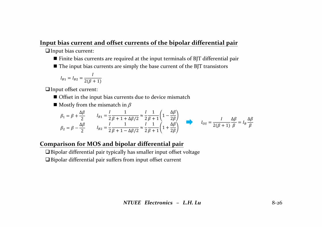
Input bias current and offset currents of the bipolar differential pairInput bias current: Finite bias currents are required at the input terminals of BJT differential pair The input bias currents are simply the base current of the BJT transistors
Input offset current: Offset in the input bias currents due to device mismatch Mostly from the mismatch in
Comparison for MOS and bipolar differential pairBipolar differential pair typically has smaller input offset voltageBipolar differential pair suffers from input offset current
NTUEE Electronics – L.H. Lu 8-26
𝛽 = 𝛽 +∆𝛽
2
𝛽 = 𝛽 −∆𝛽
2
𝐼 =𝐼
2
1
𝛽 + 1 + ∆𝛽/2≈
𝐼
2
1
𝛽 + 11 −
∆𝛽
2𝛽
𝐼 =𝐼
2
1
𝛽 + 1 − ∆𝛽/2≈
𝐼
2
1
𝛽 + 11 +
∆𝛽
2𝛽
𝐼 =𝐼
2(𝛽 + 1)
∆𝛽
𝛽= 𝐼
∆𝛽
𝛽
𝐼 = 𝐼 =𝐼
2(𝛽 + 1)
8.5 The Differential Amplifier with Active Load
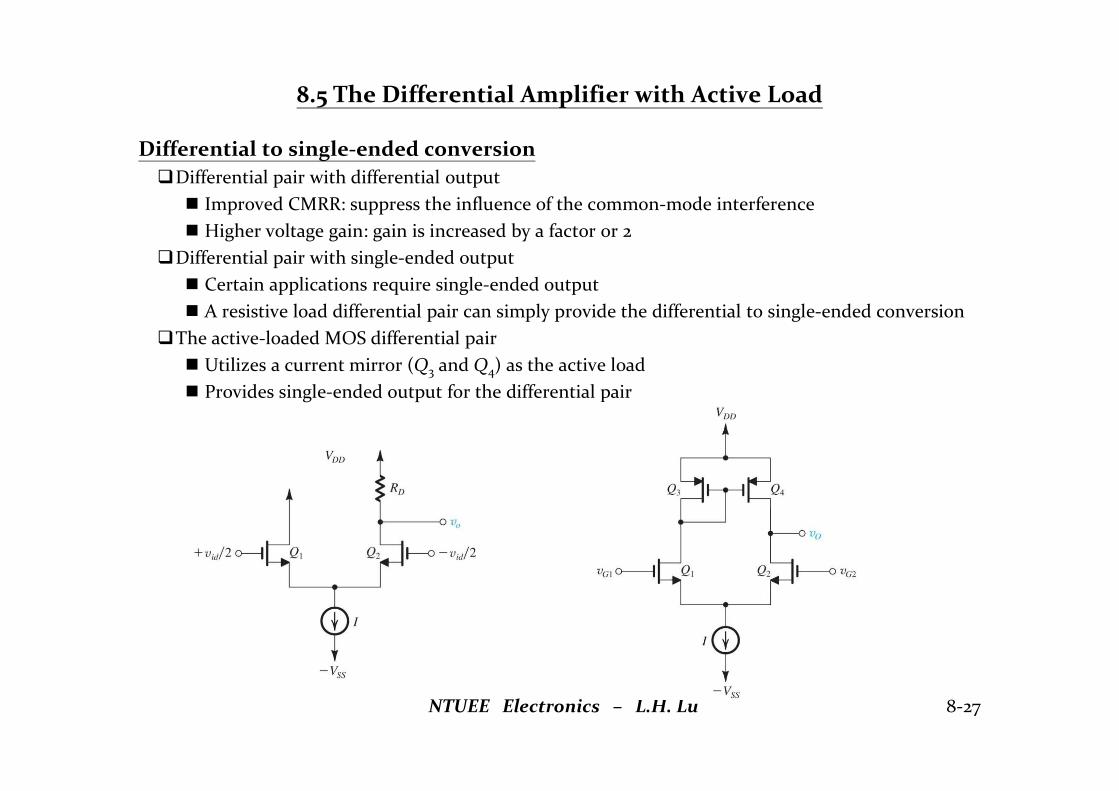
Differential to single-ended conversionDifferential pair with differential output Improved CMRR: suppress the influence of the common-mode interference Higher voltage gain: gain is increased by a factor or 2
Differential pair with single-ended output Certain applications require single-ended output A resistive load differential pair can simply provide the differential to single-ended conversion
The active-loaded MOS differential pair Utilizes a current mirror (Q3 and Q4) as the active load Provides single-ended output for the differential pair
NTUEE Electronics – L.H. Lu 8-27

Basic circuit operationQuiescent point: Perfect matching case:Bias current is equally divided for Q1 and Q2
The current of Q1 also flows through Q3
Current of Q3 is mirrored to Q4
All currents are identical (ID1 = ID2 = ID3 = ID4 = I/2) The currents of Q2 and Q4 balance outZero output current to the following stageQuiescent output voltage = VDD VSG3
Input common-mode range (ICMR):ICMRmax = VDD – VSG3 + Vtn
ICMRmin = –VSS + VCS + VGS1
Mismatch in the devices:Nonzero net current at the output nodeThe current flows into the output resistances of Q2 and Q4
The output voltage deviates from VDDVSG3
Applying differential input voltage: A difference current between Q1 and Q2
The net difference current exists at the output
NTUEE Electronics – L.H. Lu 8-28

Voltage gain of the active-loaded MOS differential pairTransconductance: Gm = gm1
The transconductance is evaluated by output current with v0 = 0 V The drain of Q3 is considered a low-impedance node and the voltage is relatively low vg3 0 V With vg3 v0 = 0 V, differential half circuit applies for Q1 and Q2 and source voltage is 0 V
NTUEE Electronics – L.H. Lu 8-29
𝑣 = −𝑔𝑣
2
1
𝑔𝑟 𝑟 ≈ −
𝑔
𝑔
𝑣
2
→ 𝐺 ≈ 𝑔 = 𝑔
𝑖 = −𝑔 𝑣 + 𝑔𝑣
2= 𝑔
𝑔
𝑔
𝑣
2+ 𝑔
𝑣
2≈ 𝑔 𝑣

Output resistance: Ro ro2||ro4
Differential gain: Ad = GmRo = gm1(ro2||ro4) gmro/2Circuit model for MOS differential amplifier with a current-mirror load
NTUEE Electronics – L.H. Lu 8-30
𝑅 =𝑟 + 𝑅
𝑔 𝑟=
1
𝑔+
1/𝑔
𝑔 𝑟≈
1
𝑔
𝑅 = 𝑅 + 𝑟 + 𝑔 𝑟 𝑅 ==1
𝑔+ 𝑟 +
2𝑟
𝑔≈ 2𝑟
𝑖 =𝑣
𝑅
𝑖 = 𝑖 + 𝑖 +𝑣
𝑟=
2𝑣
𝑅+
𝑣
𝑟
𝑅 = 𝑟 ||𝑟
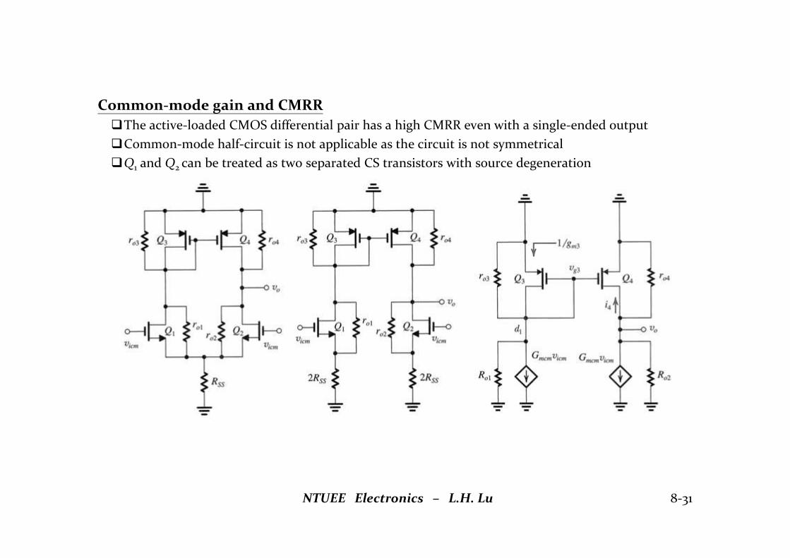
Common-mode gain and CMRRThe active-loaded CMOS differential pair has a high CMRR even with a single-ended outputCommon-mode half-circuit is not applicable as the circuit is not symmetricalQ1 and Q2 can be treated as two separated CS transistors with source degeneration
NTUEE Electronics – L.H. Lu 8-31

Common-mode gain: Acm –1/(2gm3RSS)
Common-mode rejection ratio: CMRR = gm1(ro2||ro4)(2gm3RSS)
NTUEE Electronics – L.H. Lu 8-32
𝑣 =2𝑅 ||𝑟
2𝑅 ||𝑟 + 1/𝑔𝑣 ≈ 𝑣
𝑖 =𝑣
2𝑅
𝐺 ≡𝑖
𝑣=
1
2𝑅
𝑅 = 2𝑅 + 𝑟 + 𝑔 𝑟 (2𝑅 )
𝑅 = 2𝑅 + 𝑟 + 𝑔 𝑟 (2𝑅 )
𝑣 = −𝐺 𝑣 𝑅 ||𝑟 ||1
𝑔
𝑖 = 𝑔 𝑣 = 𝑔 𝑣 = −𝑔 𝐺 𝑣 𝑅 | 𝑟 |1
𝑔
𝑖 = 𝐺 𝑣
𝑣 = 𝑖 + 𝑖 𝑅 ||𝑟 = −𝑣𝑅 ||𝑟
2𝑅1 − 𝑔 𝑅 ||𝑟 ||
1
𝑔
𝐴 ≡𝑣
𝑣≈ −
𝑟
2𝑅
1
1 + 𝑔 𝑟≈ −
1
2𝑔 𝑅

The bipolar differential pair with active loadCircuit schematic: Bipolar differential pair Q1 and Q2
Bipolar current mirror Q3 and Q4 as active load Constant current source for dc bias The bias current is equally divided for Q1 and Q2
Input resistance: Rid = 2r1
Transconductance: Gm gm1
Transconductance is evaluated by output current with vo = 0V Collector of Q3 is low-impedance node with vb3 oV Differential half circuit applies for Q1 and Q2 with emitter voltage = 0V
NTUEE Electronics – L.H. Lu 8-33
𝑣 = −𝑔𝑣
2(𝑟 | 𝑟 |𝑟 ||𝑟 ) ≈ −𝑔 𝑟
𝑣
2
𝑔 𝑣 = −𝑔 𝑔 𝑟𝑣
2
𝑖 = 𝑔𝑣
2− 𝑔 𝑣 = 𝑔 + 𝑔 𝑔 𝑟
𝑣
2
𝐺 ≡𝑖
𝑣=
1
2𝑔 + 𝑔 𝑔 𝑟 ≈ 𝑔

Output resistance (Ro):
Differential gain:
Common-mode gain:
CMRR:
NTUEE Electronics – L.H. Lu 8-34
𝑅 ≈ 𝑟 1 + 𝑔 𝑟 ||𝑟 ≈ 𝑟 1 + 𝑔 𝑟 ≈ 2𝑟
𝑖 =𝑣
𝑅=
𝑣
2𝑟
𝑖 = 2𝑖 +𝑣
𝑟=
𝑣
𝑟+
𝑣
𝑟
𝑅 ≡ = 𝑟 ||𝑟
𝐴 ≡𝑣
𝑣= 𝐺 𝑅 = 𝑔 (𝑟 ||𝑟 ) ≈
1
2𝑔 𝑟
𝐶𝑀𝑅𝑅 ≡𝐴
𝐴= 𝑔 (𝑟 ||𝑟 )
𝛽 𝑅
𝑟≈
1
2𝛽 𝑔 𝑅
𝑖 ≈ 𝑖 ≈𝑣
2𝑅
𝑣 = −𝑖1
𝑔||𝑟 ||𝑟 |𝑟
𝑣 = −𝑟 𝑔 𝑣 + 𝑖
𝐴 ≡𝑣
𝑣=
𝑟
2𝑅𝑔
1
𝑔||𝑟 ||𝑟 |𝑟 − 1
≈ −𝑟
2𝑅
2/𝑟
𝑔 + 2/𝑟≈ −
𝑟
𝛽 𝑅

Systematic input offset voltage Difference current between Q3 and Q4 due to finite Net current at output for both input terminals grounded Input offset voltage to eliminate the output current This offset has nothing to do with device mismatch
Improved current mirror can be used to reduce the systematic input offset
NTUEE Electronics – L.H. Lu 8-35
𝐼
𝐼=
1
1 + 2/𝛽
𝐼 = 𝛼𝐼/2
1 + 2/𝛽
∆𝑖 = 𝛼𝐼
21 −
1
1 + 2/𝛽= 𝛼
𝐼
2
2/𝛽
1 + 2/𝛽≈ 𝛼
𝐼
𝛽
𝑉 = −∆𝑖
𝐺= −
2𝑉
𝛽


![] bcc.ee.ntu.edu.tw/~lhlu/eecourses/Electronics3/Electronics_Ch16.pdfã Ë \ ã Ë Ë Ë ã Ë Ï \ æ Ë Ë ã](https://img.pdfslide.us/doc/110x75/5e5906cafb29d70a251fd0ad/-bcceentuedutwlhlueecourseselectronics3electronicsch16pdf-.jpg)