Embed Size (px)
Citation preview

Int. J. Nanoelectronics and Materials 10 (2017) 111-122
DC and microwave characteristics of AlN spacer based Al0.37Ga0.63N/GaN HEMT on SiC substrates for high power RF applications
P.Murugapandiyan1 , S.Ravimaran2 , J.William3
1 Research Scholar, Faculty of information and Communication, Anna University, Chennai. 2Professor, Department of Electrical and Computer Science, M.A.M College of Engineering, Trichy-India. 3Professor, Department of Electronics and Communication Engineering, M.A.M. College of Engineering and Technology, Trichy-India. Received 6 Jan 2017; Revised 25 Mar 2017; Accepted 28 Apr 2017
Abstract
The DC and RF performance of 30nm gate length enhancement mode (E-mode) AlGaN/AlN/GaN High electron mobility transistor (HEMT) on SiC substrate with heavily doped source and drain region have investigated using Synopsys TCAD tool drift diffusion model at room temperature. The proposed device features are recessed T - gate structure, InGaN back barrier and Si3N4 passivated device surface. The HEMT exhibits a maximum drain current density of 2.1 / , transconductance of 1680 / , current gain cut-off frequency frequency of 220 and power gain cut-off frequency of 245 . At room temperature the measured carrier mobility , sheet charge carrier density and breakdown voltage are 1400 / ), 1.6 10 ) and 14 respectively. The excellent DC and microwave performance of the proposed HEMT is promising candidate for future high power RF applications. Keywords: HEMT, back-barrier, recessed gate, cut-off frequency, regrown ohmic contact and short channel effects.
1. Introduction
The preeminent physical property of such as larger band gap 3.44 , breakdown field 3.3 10 / , higher saturation velocity 2.7 10 / , good thermal conductivity 1.95 and higher mobility 2000 200 / [1-2] has captivated the raptness attentions to develop high power with high frequency very large scale integration (VLSI) circuits for next generation RF applications such as high power amplifiers for space research, remote sensing, imaging systems and low noise wide bandwidth amplifiers design. In the last two decade’s several research progresses have been made to improve the DC and Microwave characteristics of GaN based HEMT [3-22]. The current gain cut-off frequency ( , power gain cut-off frequency ( and breakdown voltage ( ) of the HEMT are important parameters for
* ) For Correspondence. E-mail: [email protected]
P.Murugapandiyan, et al. / DC and microwave characteristics of AlN spacer based…
112
RF and mixed signal applications. Several progress has been made to improve the cut-off frequency of the GaN based HEMT such as InAlN/AlGaN/AlN as top barrier, InGaN/AlGaN back barrier, regrown ohmic contacts and device surface passivation [3-14]. However the breakdown voltage of the device is deteriorated when the device is scaling down below 50 nm gate length. Breakdown voltage is an essential parameter for high power applications. The higher breakdown field of GaN is the motivation for designing GaN based power amplifiers monolithic microwave integrated circuits for Sub-millimeter wave applications. Smaller breakdown voltages limit the high power RF operation of the device. In addition to that higher is required for high power amplifiers design. To enhance the
of the HEMT, proper device design is necessary in order to minimize the gate resistance (Rg), drain conductance (gd) and gate-drain capacitance (Cgd), which will reduce the parasitic time delay of the device so that fT and of GaN based HEMT are improved significantly. To improve the high frequency operation of the device the gate length (Lg) must be reduced for lower transit time of electrons. For the gate length below 50 nm device needs a thinner barrier layer to maintain the good aspect ratio Lg/d (gate length - gate to channel separation distance). Higher the aspect ratio results in suppressed drain induced barrier lowering (DIBL) [13]. A 80 nm gate length AlGaN/GaN HEMT on Si manifested a maximum / of 176/70 GHz [1]. The SiN passivated 100 nm gate length conventional rectangular gate AlGaN/GaN HEMT demonstrated a fmax 118 GHz [2] and also the minimum noise figure is demonstrated in [11] by using SiN passivation. T gate AlGaN/GaN HEMT with 0.14 gate length had shown a power gain cut-off frequency of 35 GHz [3]. 100nm gate length AlGaN/GaN HEMT with InGaN back barrier obtained / of 153/198 GHz [4]. The heavily doped source/drain region n+ GaN regrown ohmic contacts with 50 nm T gate InAlN/GaN HEMTs on SiC demonstrated / of 141/232 GHz[10]. High on/off current ratio is achieved by 50 nm gate length InAlN/GaN HEMT with SiN passivation [9]. With the improved transconductance and suppression of current collapses is demonstrated by using recessed gate AlGaN/GaN and also the short channel effect is reduced in greater extent [13]. The improved breakdown voltage of the AlGaN/GaN HEMT had shown by using AlGaN back barrier [14]. The enhanced carrier confinement, higher mobility 1300 / , improved sheet resistance of 420 [ohm/Sqr] with reduced buffer leakage is demonstrated by using 3nm InGaN back barrier in [20]. In this article, we have proposed and investigated the DC and RF characteristics of a novel 30 nm heavily doped (n+ GaN) regrown ohmic source/drain regions with recessed T-gate AlGaN/AlN/GaN HEMT. To obtain the superior carrier confinement in 2DEG with enhanced carrier mobility, . . is used as back barrier in our model. The parasitic gate capacitances are majorly suppressed by SiN passivation layer. The higher aspect ratio is maintained (Lg/d) by recessed gate structure to effectively reduce the short channel effects. The proposed novel Lg=30 nm AlGaN/GaN HEMT device shows an excellent improvement in DC and RF characteristics. The peak drain current density of 2.1 [A/mm], of 1680 [mS/mm], and / of 220/245 GHz are recorded. The observed off-state breakdown voltage of the device is 14V. The gate leakage current and SCEs are majorly suppressed and improved on/off ratio is achieved. These high DC and RF performances of the HEMT are obtained because of extreme reduction in the device parasitic resistances and capacitances.
Int. J. Nanoelectronics and Materials 10 (2017) 111-122
113
2. Device structure and Bandgap diagram:
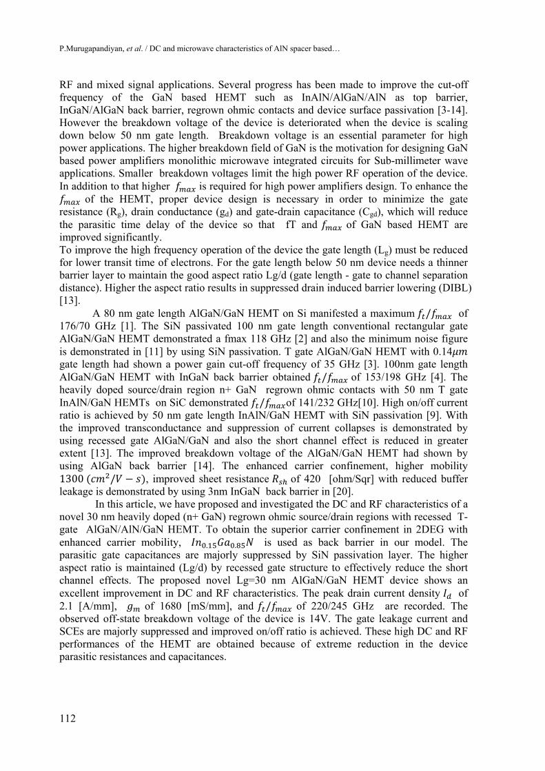
The vertical cross section of / / device structure is depicted in Fig.1. The device consists of 3 substrate to achieve good thermal stability,1450 Fe doped GaN buffer layer, which isolates the channel from the substrate defects, 3.5 back barrier layer, which helps to confine more electron in the channel due to its effective conduction band notch at the interface with channel and also it contributed for higher carrier mobility in the 2 (~1500 / ). Moreover the buffer leakage current is suppressed by the back barrier. The channel region is defined by30 and 10 nm . . is used as the top barrier layer. A very thin 1 spacer layer is placed between the barrier and channel which improves the electron mobility in the 2 by reducing the interface roughness and alloy disorder scattering at the interface of / . The source and drain regions are formed by heavily doped 50 with in the order of ~7 10 to minimize the contact resistances.The source and drain ohmic contacts are designed by using / / metal stack and shaped recessed gate is formed by / metal stack. T-gate structure having the head size of 400 , stem height of 140 with 20 footprint is designed, which liftoff wide cross sectional gate area with smaller gate length, and schottky contact is formed by / / metal stack . The drain to source separation is kept at 140 . In order to reduce the parasitic capacitances of the device, finally the device surface is fully passivated by 25 layer, which greatly helped for achieving higher cut-off frequencies and to avoid the current collapses.
Fig.1: (.a) AlGaN/AlN/GaN HEMT with InGaN back –barrier, (b) Conduction band offset.
The conduction band offset diagram of AlGaN/AlN/GaN/InGaN is depicted in Fig.1.b.Due to the induced piezoelectric polarization between InGaN and GaN, there will be a sharp raised potential barrier is formed at the back of 2DEG channel. Such a sharp notch helps to confine the electron in a better manner in the channel region and also it mitigates the buffer leakage current. A very thin 1 nm wide band gap (6.01 eV) AlN spacer is placed between barrier and channel to offer large effective conduction band offset and also it helps to reduce the gate leakage current.
P.Murugapandiyan, et al. / DC and microwave characteristics of AlN spacer based…
114
3. Results and Discussion
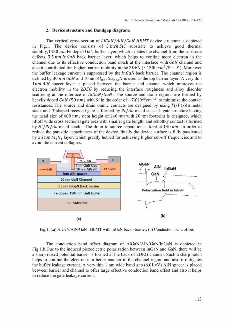
Fig.2. shows the sheet charge carrier density, mobility and sheet resistance dependency on Al content in AlxGa(1-x)N barrier layer [4]. Higher the Al content of barrier layer gives better sheet charge density but the mobility of the carriers is decreasing. In this work, a 10 nm . . barrier layer with InGaN back barrier offered a sheet carrier density of 1.6 10 and the observed mobility of electron in the 2DEG from the device structure simulation is 1450 / . The back barrier layer greatly helped to confine the electron in 2DEG region in better manner and enhanced the sheet charge density.
Fig.2: Sheet charge density, mobility, sheet resistance dependency on Al content in AlxGa(1-x)N
Barrier layer [2].
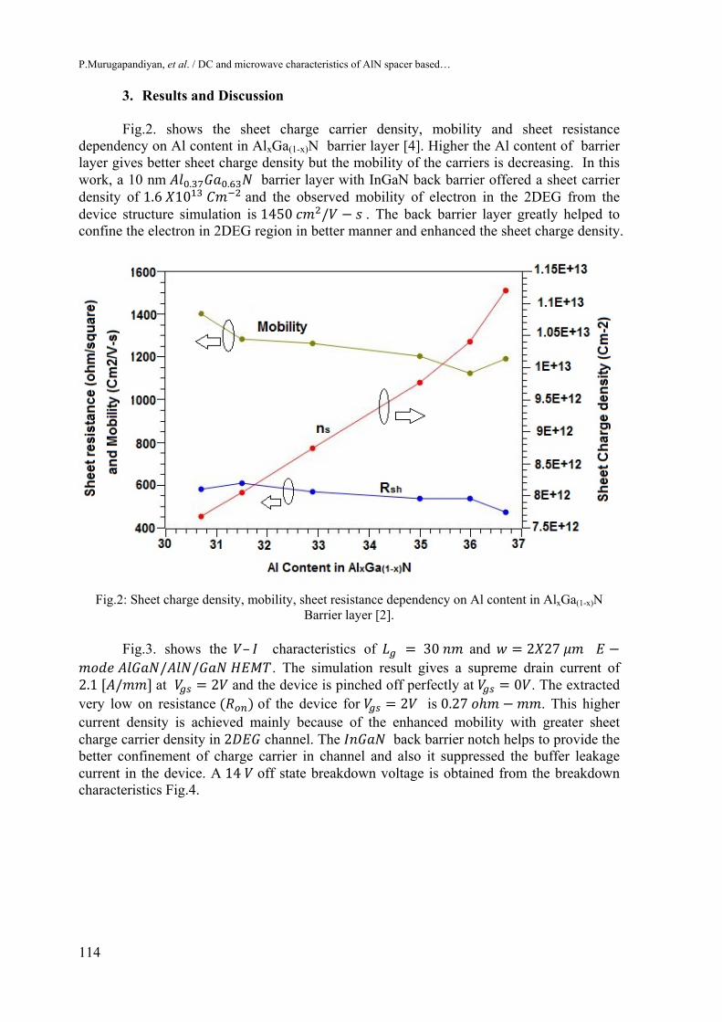
Fig.3. shows the – characteristics of 30 and 2 27 / / . The simulation result gives a supreme drain current of
2.1 / at 2 and the device is pinched off perfectly at 0 . The extracted very low on resistance of the device for 2 is 0.27 . This higher current density is achieved mainly because of the enhanced mobility with greater sheet charge carrier density in 2 channel. The back barrier notch helps to provide the better confinement of charge carrier in channel and also it suppressed the buffer leakage current in the device. A 14 off state breakdown voltage is obtained from the breakdown characteristics Fig.4.

Int. J. Nanoelectronics and Materials 10 (2017) 111-122
115
Fig.3: V-I Characteristics of = 30 nm and 2 27 E-mode AlGaN/AlN/GaN HEMT
Fig. 4: off state-breakdown characteristics of = 30 nm and 2 27 E-mode
AlGaN/AlN/GaN HEMT .
P.Murugapandiyan, et al. / DC and microwave characteristics of AlN spacer based…
116
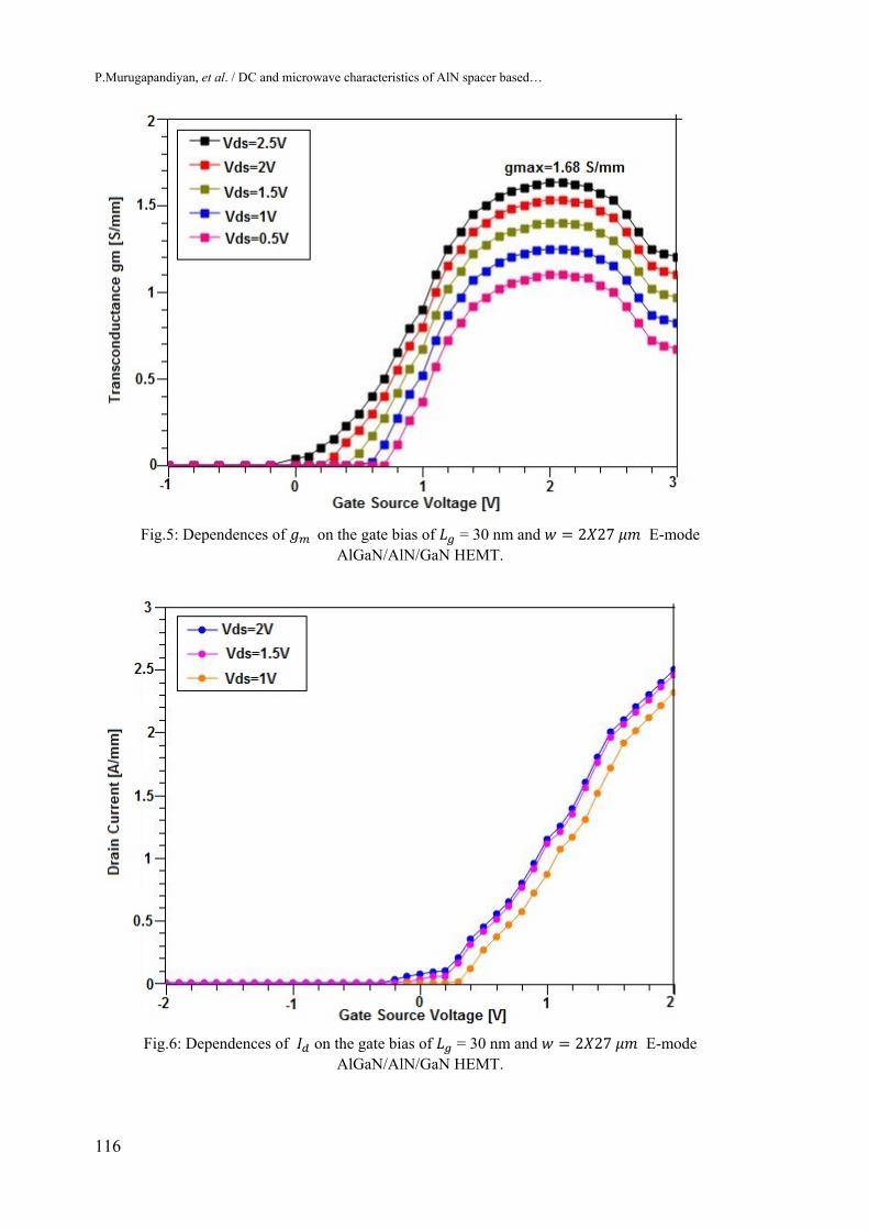
Fig.5: Dependences of on the gate bias of = 30 nm and 2 27 E-mode
AlGaN/AlN/GaN HEMT.
Fig.6: Dependences of on the gate bias of = 30 nm and 2 27 E-mode
AlGaN/AlN/GaN HEMT.

Int. J. Nanoelectronics and Materials 10 (2017) 111-122
117
Fig.5. shows the transconductance variation with the gate bias voltage. The maximum transconductance of the device is extracted from the plot is 1.68 /
2 . The extracted threshold voltage of the device from the transfer characteristics Fig.6. 0.4 .
The subthreshold and gate leakage current characteristics of = 30 nm and 2 27 E / / is shown in Fig.7. The gate leakage
current depends on the band gap of the barrier and channel materials. The higher the band gap spacer layer effectively suppressed the gate leakage current in the order of 1 10 / at 0 . The drain current on/off ratio is observed as 10 at 2 .
Fig.7: Subthreshold and gate leakage current characteristics of = 30 nm and 2 27 E-
mode AlGaN/AlN/GaN HEMT in log-scale plot.

P.Murugapandiyan, et al. / DC and microwave characteristics of AlN spacer based…
118
Fig.8: Cut-off frequencies Vs gate bias of = 30 nm and 2 27 E-mode AlGaN/AlN/GaN
HEMT for Vds=2V.
The simulation result of current gain cut-off frequency ) and power gain cut-off frequency of 30 / / is displayed in Fig.8. The obtained peak / is 220/245GHz respectively. The obtained cut-off frequencies are the best cut-off frequencies of enhancement mode / with peak drain current of 2.1 / , low gate leakage current and high on-off ratio among any AlGaN/GaN device structure so far from author’s knowledge. The higher / is achieved by a drastic reduction in the contacts resistances and parasitic capacitance of the device mainly because of heavily doped source / drain regions has direct contacts with the channel, combined with ~50 drain and source access region and passivated device surface. The features of recessed T-gate structure is escalated transconductance and the attenuated drain conductance also contributed to achieve this higher . The expression for are written as follows;
Current gain Cut-off frequency /
. /
(1)
Power gain cut-off frequency
(2)
where the source resistance .
and drain resistance .
. is the contact resistance and denotes the channel sheet resistance,
respectively. is thgate to source distance and is the gate to drain separation, respectively. is the width of the gate. is the gate access resistance and represents
Int. J. Nanoelectronics and Materials 10 (2017) 111-122
119
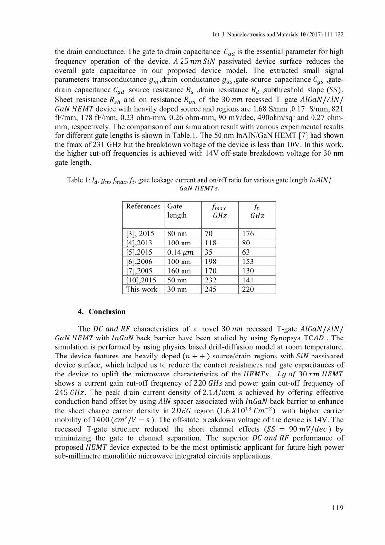
the drain conductance. The gate to drain capacitance is the essential parameter for high frequency operation of the device. 25 passivated device surface reduces the overall gate capacitance in our proposed device model. The extracted small signal parameters transconductance ,drain conductance ,gate-source capacitance ,gate-drain capacitance ,source resistance ,drain resistance ,subthreshold slope , Sheet resistance and on resistance of the 30 recessed T gate / /
device with heavily doped source and regions are 1.68 S/mm ,0.17 S/mm, 821 fF/mm, 178 fF/mm, 0.23 ohm-mm, 0.26 ohm-mm, 90 mV/dec, 490ohm/sqr and 0.27 ohm-mm, respectively. The comparison of our simulation result with various experimental results for different gate lengths is shown in Table.1. The 50 nm InAlN/GaN HEMT [7] had shown the fmax of 231 GHz but the breakdown voltage of the device is less than 10V. In this work, the higher cut-off frequencies is achieved with 14V off-state breakdown voltage for 30 nm gate length.
Table 1: , , , ,gate leakage current and on/off ratio for various gate length / .
References Gate
length
[3], 2015 80 nm 70 176 [4],2013 100 nm 118 80 [5],2015 0.14 35 63 [6],2006 100 nm 198 153 [7],2005 160 nm 170 130 [10],2015 50 nm 232 141 This work 30 nm 245 220
4. Conclusion
The characteristics of a novel 30 recessed T-gate / / with back barrier have been studied by using Synopsys TC . The
simulation is performed by using physics based drift-diffusion model at room temperature. The device features are heavily doped source/drain regions with passivated device surface, which helped us to reduce the contact resistances and gate capacitances of the device to uplift the microwave characteristics of the . 30 shows a current gain cut-off frequency of 220 and power gain cut-off frequency of 245 . The peak drain current density of 2.1 / is achieved by offering effective conduction band offset by using spacer associated with back barrier to enhance the sheet charge carrier density in 2 region 1.6 10 with higher carrier mobility of 1400 / ). The off-state breakdown voltage of the device is 14V. The recessed T-gate structure reduced the short channel effects 90 / by minimizing the gate to channel separation. The superior performance of proposed device expected to be the most optimistic applicant for future high power sub-millimetre monolithic microwave integrated circuits applications.

P.Murugapandiyan, et al. / DC and microwave characteristics of AlN spacer based…
120
Acknowledgments The authors acknowledge the Nanoelectron Devices and Circuits Laboratory of
Electronics and Communication Engineering Department at M.A.M College of Engineering, Trichy-India for providing all facilities to carry out this research work.
References
[1] Liu William, Fundamentals of III–V devices HBT’s, MESFETs, and HFETs/HEMTs. John Wiley & Sons, Inc.; 1999
[2] Piprek Joachim. Nitride Semiconductor Devices Principles and Simulation. Weinheim: WILEY-VCH Verlag GmbH & Co KGaA; 2007
[3] 1.Wael Jatal, Uwe Baumann, Katja Tonisch, Frank Schwierz, and Jörg Pezoldt “High-Frequency Performance of GaN High-Electron Mobility Transistors on 3C-SiC/Si Substrates With Au-Free Ohmic Contacts” IEEE Electron device letters, 36 (2), February 2015. doi: 10.1109/LED.2014.2379664
[4] Dirk Schwantuschke, Peter Brückner, Rüdiger Quay, Michael Mikulla and Oliver Ambacher “High-Gain Millimeter-Wave AlGaN/GaN Transistors” IEEE Transactions on electron devices, vol. 60, no. 10, october 2013. doi: 10.1109/TED.2013.2272180
[5] Robert C. et.al. “Implementation of High-Power-Density X-Band AlGaN/GaN High Electron Mobility Transistors in a Millimeter-Wave Monolithic Microwave Integrated Circuit Process” IEEE electron device letters, 36 (10), october 2015. doi:10.1109/LED.2015.2474265
[6] T. Palacios, A. Chakraborty, S. Heikman, S. Keller, S. P. DenBaars and U. K. Mishra, “AlGaN/GaN High Electron Mobility Transistors With InGaN Back-Barriers” IEEE Electron device letters, 27 (1), January 2006. doi: 10.1109/LED.2005.860882
[7] T. Palacios, A. Chakraborty, S. Rajan, C. Poblenz, S. Keller,S. P. DenBaars, J. S. Speck and U. K. Mishra, “High-Power AlGaN/GaN HEMTs for Ka-Band Applications” IEEE Electron device letters, 26 (11), November 2005. doi: 10.1109/LED.2005.857701
[8] Faiza Afroz Faria, Jia Guo, Pei Zhao, Guowang Li, Prem Kumar Kandaswamy et al. “Ultra-low resistance ohmic contacts to GaN with high Si doping concentrations grown by molecular beam epitaxy” Appl. Phys. Lett. 101, 032109 (2012); doi: 10.1063/1.4738768
[9] Lorenzo Lugani, Jean-François Carlin, Marcel A. Py, Denis Martin, Francesca Rossi, Giancarlo Salviati, Patrick Herfurth, Erhard Kohn, Jürgen Bläsing, Alois Krost and Nicolas Grandjean “Ultrathin InAlN/GaN heterostructures on sapphire for high on/off current ratio high electron mobility transistors” Journal of Applied Physics 113, 214503 (2013); doi: 10.1063/1.4808260
[10] Diego Marti, Stefano Tirelli, Valeria Teppati, Lorenzo Lugani,Jean-François Carlin, Marco Malinverni, Nicolas Grandjean and C. R. Bolognesi “94-GHz Large-Signal Operation of AlInN/GaN High-Electron-Mobility Transistors on Silicon with Regrown Ohmic Contacts” IEEE Electron device letters, 36 (1), January 2015. doi: 10.1109/LED.2014.2367093
[11] Z. H. Liu,S. Arulkumaran and G. I. Ng, “Improved Microwave Noise Performance by SiN Passivation in AlGaN/GaN HEMTs on Si” IEEE Microwave and wireless components letters, 19 (6), June 2009. doi: 10.1109/LMWC.2009.2020027
[12] Jia Guo et.al “MBE-Regrown Ohmics in InAlN HEMTs with a Regrowth Interface Resistance of 0.05 Ω · mm” IEEE Electron device letters, 33 (4), April 2012. doi: 10.1109/LED.2012.2186116
Int. J. Nanoelectronics and Materials 10 (2017) 111-122
121
[13] Subramaniam ARULKUMARAN_, Takashi EGAWAy, Lawrence SELVARAJ and Hiroyasu ISHIKAWA “On the Effects of Gate-Recess Etching in Current-Collapse of Different Cap Layers Grown AlGaN/GaN High-Electron-Mobility Transistors” Japanese Journal of Applied Physics , 45 (8), 2006, L220–L223.
[14] Sheng Lei Zhao, Bin Hou, Wei Wei Chen, Min Han Mi, Jia Xin Zheng, Jin Cheng Zhang, Xiao Hua Ma and Yue Hao “Analysis of the Breakdown Characterization Method in GaN-Based HEMTs” IEEE Transactions on power electronics, 31 (2), February 2016. doi: 10.1109/TPEL.2015.2416773
[15] Johan Bergsten, Jr-Tai Chen, Sebastian Gustafsson, Anna Malmros, Urban Forsberg,Mattias Thorsell, Erik Janzén and Niklas Rorsman, “Performance Enhancement of Microwave GaN HEMTs Without an AlN-Exclusion Layer Using an Optimized AlGaN/GaN Interface Growth Process” IEEE Transactions on electron devices, 63 (1), January 2016
[16] Chih-Hao Wang, Shin-Yi Ho and Jian Jang Huang, “Suppression of Current Collapse in Enhancement-Mode AlGaN/GaN High Electron Mobility Transistors” IEEE Electron device letters, 37 (1), January 2016. doi: 10.1109/LED.2015.2498623
[17] Tian-Li Wu, Denis Marcon, Shuzhen You, Niels Posthuma, Benoit Bakeroot,Steve Stoffels, Marleen Van Hove, Guido Groeseneken and Stefaan Decoutere “Forward Bias Gate Breakdown Mechanism in Enhancement-Mode p-GaN Gate AlGaN/GaN High-Electron Mobility Transistors” IEEE Electron device letters, 36 (10), October 2015. Digital Object Identifier 10.1109/LED.2015.2465137
[18] Xinhua Wang, Sen Huang, Yingkui Zheng, Ke Wei, Xiaojuan Chen, Haoxiang Zhang and Xinyu Liu “Effect of GaN Channel Layer Thickness on DC and RF Performance of GaN HEMTs With Composite AlGaN/GaN Buffer” IEEE Transactions on electron devices, 61 (5), May 2014. doi: 10.1109/TED.2014.2312232