Embed Size (px)
Citation preview
www.f1-media.com
F1M84
Datasheet
Confidential / Preliminary Documentation
Revision 2.0
F1media
www.f1-media.com
List of Contents 1. General
1.1 Overview
1.2 Features
1.3 Application
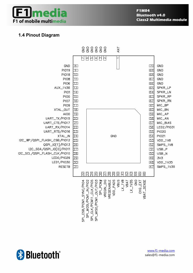
1.4 Pinout Diagram
1.5 Device Terminal Functions
1.6 Module Dimension
2. Characteristics
2.1 Electrical Characteristics
2.2 RF Characteristics
3. Interface
3.1 UART interface
3.2 USB interface
3.3 Serial Flash interface
3.4 Programming and Debug interface
3.5 I2C EEPROM interface
3.6 LED drivers
3.7 Audio Interfaces
3.8 Battery Charger
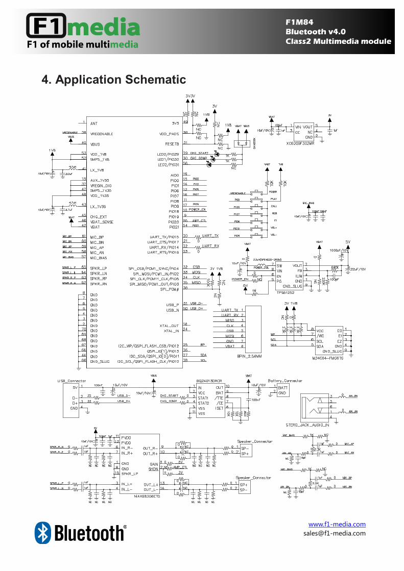
4. Application Schematic
5. PCB Layout
6. Reflow Temperature Profile
7. Revision History
www.f1-media.com
1. General
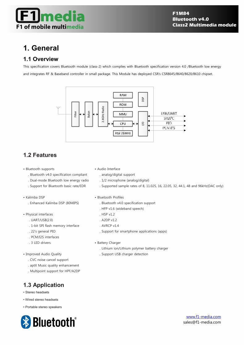
1.1 Overview This specification covers Bluetooth module (class-2) which complies with Bluetooth specification version 4.0 /Bluetooth low energy
and integrates RF & Baseband controller in small package. This Module has deployed CSR’s CSR8645/8640/8620/8610 chipset.
Fil
ter
Ba
lun
2.4
GH
z R
ad
io
DS
PI/
O
1.2 Features
• Bluetooth supports
. Bluetooth v4.0 specification compliant
. Dual-mode Bluetooth low energy radio
. Support for Bluetooth basic rate/EDR
• Kalimba DSP
. Enhanced Kalimba DSP (80MIPS)
• Physical interfaces
. UART/USB(2.0)
. 1-bit SPI flash memory interface
. 22’s general PIO
. PCM/I2S interfaces
. 3 LED drivers
• Improved Audio Quality
. CVC noise cancel support
. aptX Music quality enhancement
. Multipoint support for HPF/A2DP
• Audio Interface
. analog/digital support
. 1/2 microphone (analog/digital)
. Supported sample rates of 8, 11.025, 16, 22.05, 32, 44.1, 48 and 96kHz(DAC only)
• Bluetooth Profiles
. Bluetooth v4.0 specification support
. HFP v1.6 (wideband speech)
. HSP v1.2
. A2DP v1.2
. AVRCP v1.4
. Support for smartphone applications (apps)
• Battery Charger
. Lithium ion/Lithium polymer battery charger
. Support USB charger detection
1.3 Application • Stereo headsets
• Wired stereo headsets
• Portable stereo speakers
www.f1-media.com
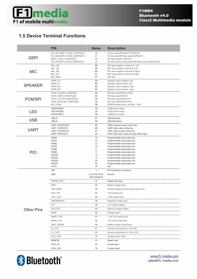
1.5 Device Terminal Functions
PIN Name Description
QSPI
I2C_SCL/QSPI_FLASH_CLK/PIO[10]
I2C_SDA/QSPI_FLASH_IO[0]/PIO[11]
QSPI_FLASH_IO[1]/PIO[13]
I2C_WP/QSPI_FLASH_CSB/PIO[12]
28
27
26
25
I2C bus clock/SPI flash CLK/PIO[10]
I2C bus data/SPI flash data bit0/PIO[11]
SPI flash data bit 1/PIO[13]
I2C bus memory write protect/SPI flash chip enable/PIO[12]
MIC
MIC _AN
MIC _AP
MIC _BN
MIC _BP
MIC_BIAS
58
59
60
61
57
MIC input negative, channel A , Left
MIC input positive, channel A, Left
MIC input negative, channel B, Right
MIC input positive, channel B, Right
MIC bias
SPEAKER
SPKR_LN
SPKR_LP
SPKR_RN
SPKR_RP
64
65
62
63
Speaker output negative, left
Speaker output positive, left
Speaker output negative, right
Speaker output positive , right
PCM/SPI
PCM1_CLK/SPI_CLK/PIO[5]
PCM1_IN/SPI_MOSI/PIO[2]
PCM1_OUT/SPI_MISO/PIO[3]
PCM1_SYNC/SPI_CSB/PIO[4]
SPI_PCM#
34
33
35
32
36
SPI data clock/PCM CLOCK
SPI data input/PCM IN
SPI data output/PCM OUT
SPI chip select/PCM SYNC
SPI/PCM select input. (0:PCM/, 1:SPI)
LED LED0/PIO[29]
LED1/PIO[30]
LED2/PIO[31]
29
30
56
LED[0] drive output
LED[1] drive output
LED[2] drive output
USB USB_P
USB_N
51
50
USB data Plus
USB data Minus
UART
UART_RTS/PIO[16]
UART_TX/PIO[15]
UART_CTS/PIO[17]
UART_RX/PIO[14]
23
20
21
22
UART request to send, active low
UART data output, active low
UART clear to send, active low
UART data input, active low (idle status high)
PIO
PIO[0]
PIO[1]
PIO[6]
PIO[7]
PIO[8]
PIO[9]
PIO[18]
PIO[19]
PIO[20]
PIO[21]
AIO[0]
15
14
12
16
11
17
10
9
55
54
19
Programmable input/output line
Programmable input/output line
Programmable input/output line
Programmable input/output line
Programmable input/output line
Programmable input/output line
Programmable input/output line
Programmable input/output line
Programmable input/output line
Programmable input/output line
AIO
Other Pins
ANT 1 RF Connection to Antenna
GND 2,3,4,5,6,7,8,44,
66,67,68,69,70
Ground
VREGIN_DIG 37 Digital LDO input
VBAT 42 Battery voltage input
VDD_PADS 39 Positive Supply input for input/output ports
VDD_1V8 53 1.8V supply input
VDD_1V35 48 1.35V supply input
VREGENABLE 38 Regulator enable input
3V3 49 3.3V output voltage
CHG_EXT 45 External charger control
VBUS 40 Charger input
SMPS_1V35 47 1.35V LDO sense input
SMPS_1V8 52 1.8V LDO sense input
VBAT_SENSE 46 Battery charger sense input
LX_1V8 41 Inductor connection for 1.8V LDO
LX_1V35 43 Inductor connection for 1.35V LDO
AUX_1V35 13 Auxiliary input 1.35V
RESETB 31 Reset if low.
XTAL_IN 24 Crystal input
XTAL_OUT 18 Crystal output
www.f1-media.com
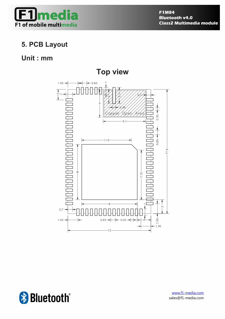
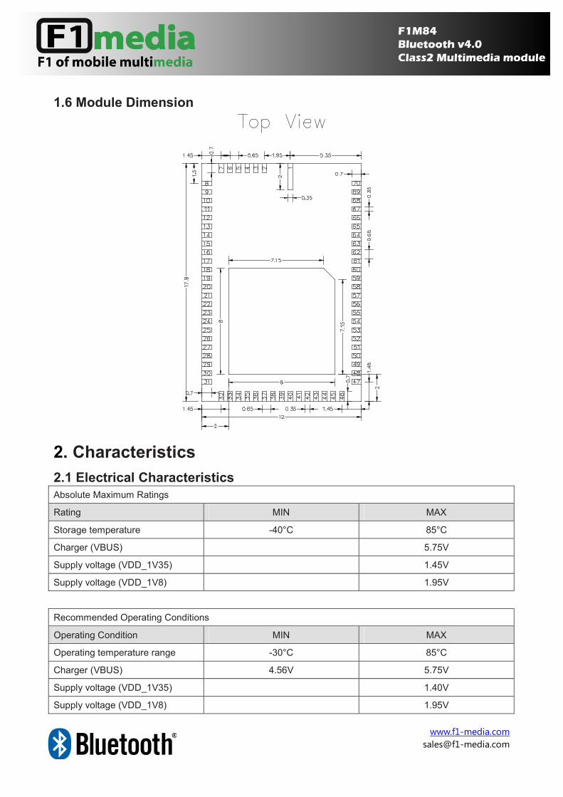
1.6 Module Dimension
2. Characteristics
2.1 Electrical Characteristics
Absolute Maximum Ratings
Rating MIN MAX
Storage temperature -40°C 85°C
Charger (VBUS) 5.75V
Supply voltage (VDD_1V35) 1.45V
Supply voltage (VDD_1V8) 1.95V
Recommended Operating Conditions
Operating Condition MIN MAX
Operating temperature range -30°C 85°C
Charger (VBUS) 4.56V 5.75V
Supply voltage (VDD_1V35) 1.40V
Supply voltage (VDD_1V8) 1.95V
www.f1-media.com
2.2 RF Characteristics
Transmitter
Specification Condition MIN TYP MAX UNIT
Output transmit power Normal -6 1 4 dBm
Transmit power density Normal 4 dBm
Transmit power control Normal 2 8 dBm
Frequency Range Normal 2400 2483.5 MHz
20dB bandwidth for modulated carrier Normal 850 1000 KHz
Adjacent channel transmit power
±2MHz
±3MHz
±4MHz
-20
-40
-40
dBm
Modulation Characteristics
f1avg
f2max
f2avg / f1avg
140
115
175
80
KHz
KHz
%
Initial carrier frequency tolerance Normal -20 20 KHz
Carrier frequency Drift
One slot packet(DH1)
Three slot packet(DH3)
Five slot packet(DH5)
-25
-40
-40
25
40
40
KHz
Transceiver
Specification Condition MIN TYP MAX UNIT
Adjacent channel transmit power
30MHz ~ 1GHz
1GHz ~12.75GHz
1.8GHz ~5.1GHz
5.1GHz ~5.3GHz
-36
-30
-47
-47
dBm
Receiver
Specification Condition MIN TYP MAX UNIT
Sensitivity level (0.1% BER) Single slot packets -70 -78 dBm
Transmit power density Multi slot packet -70 -78 dBm
C/I performance
co-channel
1MHz (Adjacent channel)
2MHz (2nd Adjacent channel)
3MHz (3rd Adjacent channel)
11
0
-30
-40
dB
Blocking performance
30MHz ~ 2000MHz
2000MHz ~ 2400MHz
2500MHz ~ 3000MHz
3000MHz ~ 12.75GHz
-10
-27
-27
-10
dBm
Intermodulation performance n=5 -39 dBm
Maximum input level -20 -10 dBm
www.f1-media.com
3. Interface
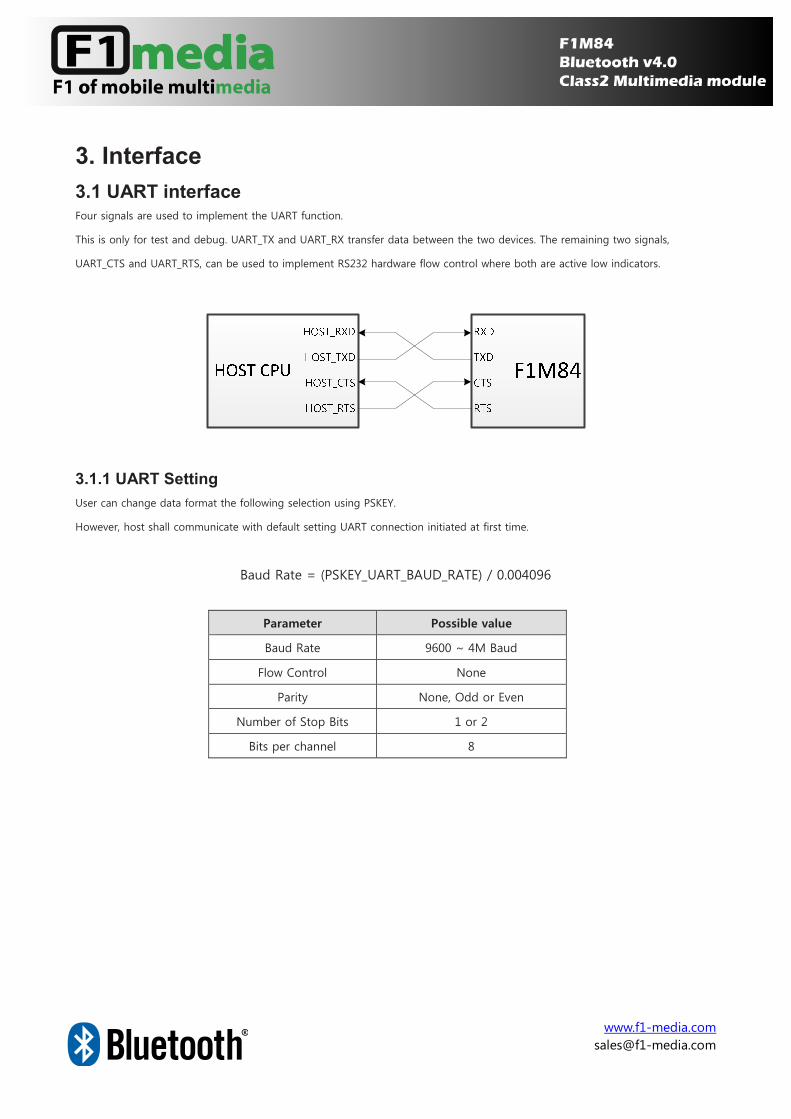
3.1 UART interface Four signals are used to implement the UART function.
This is only for test and debug. UART_TX and UART_RX transfer data between the two devices. The remaining two signals,
UART_CTS and UART_RTS, can be used to implement RS232 hardware flow control where both are active low indicators.
3.1.1 UART Setting
User can change data format the following selection using PSKEY.
However, host shall communicate with default setting UART connection initiated at first time.
Baud Rate = (PSKEY_UART_BAUD_RATE) / 0.004096
Parameter Possible value
Baud Rate 9600 ~ 4M Baud
Flow Control None
Parity None, Odd or Even
Number of Stop Bits 1 or 2
Bits per channel 8
www.f1-media.com
3.2 USB interface F1M84 has a full speed(12Mbps) USB interface for communicating with other compatible digital devices. F1M84 contains internal
USB termination resistors and requires no external resistor matching. F1M84 supports the Universal serial bus specification, battery
charging specification together.
The below describes USB basics and architecture.
- Power distribution for high and low bus-powered configurations
- Power distribution for self-powered configuration, which includes USB VBUS monitoring
- USB enumeration
- USB suspend modes and Bluetooth low-power modes :
. Global suspend
. Selective suspend, includes remote wake
. Wake on Bluetooth, includes permitted devices and set-up prior to selective suspend
. Suspend mode current draw
. PIO status in suspend mode
. Resume, detach and wake PIOs
- Battery charging from USB, which describes dead battery provision, charge currents, charging in suspend modes and USB
VBUS voltage consideration
3.3 Serial Flash interface F1M84 supports external serial flash ICs. This enables additional data storage areas for device-specific data. F1M84 supports serial
single I/O devices with a 1-bit I/O flash-memory interface.
3.4 Programming and Debug interface F1M84 provides a debug SPI interface for programming
3.5 I2C EEPROM interface F1M84 supports optional I2C eeprom for storage of setting value and voice prompt data
3.6 LED drivers F1M84 includes a 3-pad synchronized PWM LED driver for driving RGB LEDs for producing a wide range of colors. All LEDs are
controlled by firmware. The terminals are open-drain outputs, so the LED must be connected from a positive supply rail to the pad
in series with a current-limiting resistor.
3.7 Audio Interfaces
www.f1-media.com
F1M84’s audio interface consists below.
- Stereo/dual-mono audio codec
- Dual analogue audio inputs
- Dual analogue audio outputs
- 2 digital microphone inputs
- Configurable PCM and I2S interface
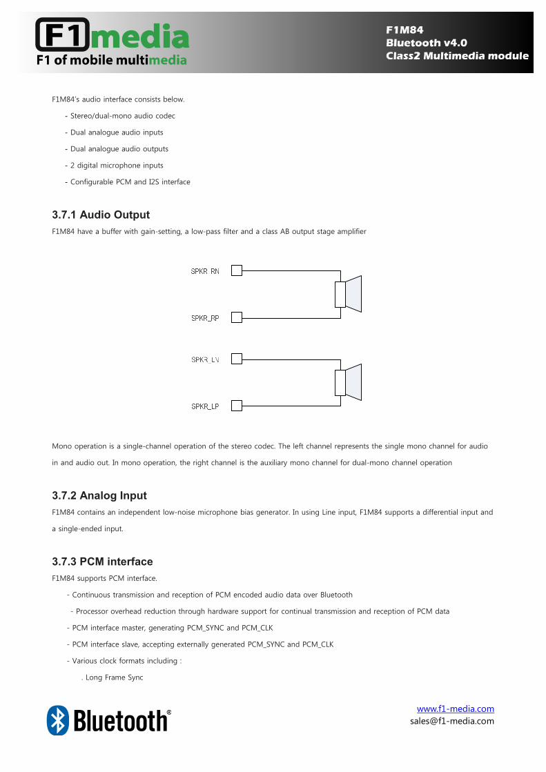
3.7.1 Audio Output
F1M84 have a buffer with gain-setting, a low-pass filter and a class AB output stage amplifier
Mono operation is a single-channel operation of the stereo codec. The left channel represents the single mono channel for audio
in and audio out. In mono operation, the right channel is the auxiliary mono channel for dual-mono channel operation
3.7.2 Analog Input
F1M84 contains an independent low-noise microphone bias generator. In using Line input, F1M84 supports a differential input and
a single-ended input.
3.7.3 PCM interface
F1M84 supports PCM interface.
- Continuous transmission and reception of PCM encoded audio data over Bluetooth
- Processor overhead reduction through hardware support for continual transmission and reception of PCM data
- PCM interface master, generating PCM_SYNC and PCM_CLK
- PCM interface slave, accepting externally generated PCM_SYNC and PCM_CLK
- Various clock formats including :
. Long Frame Sync
www.f1-media.com
. Short Frame Sync
. GCI timing environments
- 13-bit or 16-bit linear, 8-bit u-law or A-law companded sample formats
- Receives and transmits on any selection of 3 of the first 4 slots following PCM_SYNC
3.7.4 I2S Interface
The digital audio interface supports the industry standard formats for I2S, left-justified or right-justified. The interface shares the
same pins as the PCM interface, which means each audio bus is mutually exclusive in its usage.
3.8 Battery Charger
3.8.1 Battery Charger Hardware Operating Modes
The battery charger has 5 modes.
- Disabled
- Trickle charge
- Fast charge
- Standby : fully charged or float charge
- Error : charging input voltage.
The battery charger operating mode is determined by the battery voltage and current. The internal charger circuit can provide up
to 200mA. For currents higher than this, external pass transistor is need.
3.8.1.1 Disable mode
In this mode, the battery charger is fully disabled and draws no active current on any of its terminals.
3.8.1.2 Trickle Charge mode
In this mode, a current of approximately 10% of the fast charge current.
3.8.1.3 Fast Charge mode
In this mode, a current of approximately is between 10mA and 200mA.
3.8.1.4 Standby mode
When the battery is fully charged, the charger enters standby mode, and battery charging stops.
3.8.1.5 Error mode
The charger enters the error mode if the voltage on the VBUS pin is too low to operate the charger correctly. In this mode,
charging is stopped. The battery charger does not require a reset to resume normal operation.
www.f1-media.com
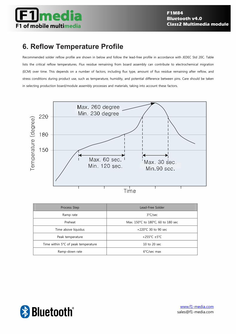
6. Reflow Temperature Profile
Recommended solder reflow profile are shown in below and follow the lead-free profile in accordance with JEDEC Std 20C. Table
lists the critical reflow temperatures. Flux residue remaining from board assembly can contribute to electrochemical migration
(ECM) over time. This depends on a number of factors, including flux type, amount of flux residue remaining after reflow, and
stress conditions during product use, such as temperature, humidity, and potential difference between pins. Care should be taken
in selecting production board/module assembly processes and materials, taking into account these factors.
Process Step Lead-Free Solder
Ramp rate 3°C/sec
Preheat Max. 150°C to 180°C, 60 to 180 sec
Time above liquidus +220°C 30 to 90 sec
Peak temperature +255°C ±5°C
Time within 5°C of peak temperature 10 to 20 sec
Ramp-down rate 6°C/sec max

www.f1-media.com
7. Revision History
Revision Date Change Descriptions Issued by
Rev 1.0 2012-10-10 Initial release S.J.LEE
Rev 2.0 2013-09-24 Added Antenna And pinmap change como