Embed Size (px)
Citation preview
Data SheetAD4630-24
24-Bit, 2 MSPS, Dual Channel SAR ADC
Rev. 0DOCUMENT FEEDBACK
TECHNICAL SUPPORT
Information furnished by Analog Devices is believed to be accurate and reliable "as is". However, no responsibility is assumed by AnalogDevices for its use, nor for any infringements of patents or other rights of third parties that may result from its use. Specifications subject tochange without notice. No license is granted by implication or otherwise under any patent or patent rights of Analog Devices. Trademarks andregistered trademarks are the property of their respective owners.
FEATURES
High performance Throughput: 2 MSPS per channel maximum INL: ±0.9 ppm maximum from −40°C to +125°C SNR: 105.7 dB typical THD: −127 dB typical NSD: −166 dBFS/Hz typical
Low power 15 mW per channel at 2 MSPS 1.5 mW per channel at 10 kSPS
Easy Drive features reduce system complexity Very low 0.6 μA input current for dc inputs Wide input common-mode range: −(1/128) × VREF to
+(129/128) × VREF Flexible external reference voltage range: 4.096 V to 5 V
Accurate integrated reference buffer with 2 μF bypasscapacitor
Programmable block averaging filter with up to 216 decimation Extended sample resolution to 30 bits Overrange and synchronization bits
Flexi-SPI digital interface 1, 2, or 4 SDO lanes per channel allows slower SCK Echo clock mode simplifies use of digital isolator Compatible with 1.2 V to 1.8 V logic
7 mm × 7 mm 64-Ball CSP_BGA package with internal supplyand reference capacitors to help reduce system footprint
APPLICATIONS
Automatic test equipment Digital control loops Medical instrumentation Seismology Semiconductor manufacturing Scientific instrumentation
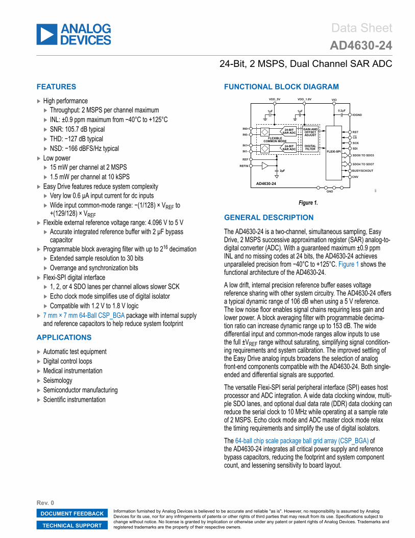
FUNCTIONAL BLOCK DIAGRAM
Figure 1.
GENERAL DESCRIPTION
The AD4630-24 is a two-channel, simultaneous sampling, EasyDrive, 2 MSPS successive approximation register (SAR) analog-to-digital converter (ADC). With a guaranteed maximum ±0.9 ppmINL and no missing codes at 24 bits, the AD4630-24 achievesunparalleled precision from −40°C to +125°C. Figure 1 shows thefunctional architecture of the AD4630-24.A low drift, internal precision reference buffer eases voltagereference sharing with other system circuitry. The AD4630-24 offersa typical dynamic range of 106 dB when using a 5 V reference.The low noise floor enables signal chains requiring less gain andlower power. A block averaging filter with programmable decima-tion ratio can increase dynamic range up to 153 dB. The widedifferential input and common-mode ranges allow inputs to usethe full ±VREF range without saturating, simplifying signal condition-ing requirements and system calibration. The improved settling ofthe Easy Drive analog inputs broadens the selection of analogfront-end components compatible with the AD4630-24. Both single-ended and differential signals are supported.The versatile Flexi-SPI serial peripheral interface (SPI) eases hostprocessor and ADC integration. A wide data clocking window, multi-ple SDO lanes, and optional dual data rate (DDR) data clocking canreduce the serial clock to 10 MHz while operating at a sample rateof 2 MSPS. Echo clock mode and ADC master clock mode relaxthe timing requirements and simplify the use of digital isolators.The 64-ball chip scale package ball grid array (CSP_BGA) ofthe AD4630-24 integrates all critical power supply and referencebypass capacitors, reducing the footprint and system componentcount, and lessening sensitivity to board layout.

Data Sheet AD4630-24TABLE OF CONTENTS
analog.com Rev. 0 | 2 of 49
Features................................................................ 1Applications........................................................... 1Functional Block Diagram......................................1General Description...............................................1Specifications........................................................ 3
Timing Specifications......................................... 5Absolute Maximum Ratings................................. 11
Thermal Resistance..........................................11Electrostatic Discharge (ESD) Ratings.............11ESD Caution.....................................................11
Pin Configuration and Function Descriptions...... 12Typical Performance Characteristics................... 14Terminology......................................................... 18
Integral Nonlinearity Error (INL)....................... 18Differential Nonlinearity Error (DNL).................18Zero Error (ZE).................................................18Gain Error (GE)................................................ 18Spurious-Free Dynamic Range (SFDR)...........18Effective Number of Bits (ENOB)..................... 18Total Harmonic Distortion (THD)...................... 18Dynamic Range (DR)....................................... 18Signal-to-Noise Ratio (SNR)............................ 18Signal-to-Noise-and-Distortion (SINAD)Ratio...............................................................18
Aperture Delay................................................. 18Transient Response......................................... 18Common-Mode Rejection Ratio (CMRR).........18Power Supply Rejection Ratio (PSRR)............ 18
Theory of Operation.............................................19Overview.......................................................... 19Converter Operation.........................................20Transfer Function............................................. 20Analog Features...............................................20Digital Sample Processing Features................ 21
Applications Information...................................... 23Typical Application Diagrams........................... 23Analog Front-End Design.................................24Reference Circuitry Design ............................. 24Device Reset....................................................25
Power Supplies................................................ 25Serial Interface.................................................... 26
SPI Signals.......................................................26Sample Conversion Timing and DataTransfer.......................................................... 28
Clocking Modes ...............................................29Data Clocking Requirements and Timing.........32
Layout Guidelines................................................36Registers............................................................. 37Register Details................................................... 38
Interface Configuration A Register................... 38Interface Configuration B Register................... 38Device Configuration Register..........................39Chip Type Register...........................................39Product ID Low Register.................................. 39Product ID High Register..................................39Chip Grade Register.........................................40Scratchpad Register.........................................40SPI Revision Register...................................... 40Vendor ID Low Register................................... 41Vendor ID High Register...................................41Stream Mode Register..................................... 41Interface Configuration C Register...................42Interface Status A Register.............................. 42Exit Configuration Mode Register.....................42Averaging Mode Register.................................43Channel 0 Offset Registers.............................. 43Channel 1 Offset Registers.............................. 44Channel 0 Gain Registers................................ 45Channel 1 Gain Registers................................ 45Modes Register................................................ 46Internal Oscillator Register...............................46Output Driver Register......................................47Test Pattern Registers......................................47Digital Diagnostics Register............................. 48Digital Errors Register...................................... 48
Outline Dimensions............................................. 49Ordering Guide.................................................49Evaluation Boards............................................ 49
REVISION HISTORY
11/2021—Revision 0: Initial Version
Data Sheet AD4630-24SPECIFICATIONS
analog.com Rev. 0 | 3 of 49
VDD_5V = 5.4 V, VDD_1.8V = 1.8 V, VIO = 1.8 V, REFIN = 5 V, input common mode = 2.5 V, fS = 2 MSPS, and all specifications TMIN to TMAX,unless otherwise noted. Typical values are at TA = 25°C.
Table 1.Parameter Test Conditions/Comments Min Typ Max UnitRESOLUTION 24 BitsANALOG INPUT
Voltage Range VIN+ − VIN− −(65/64) × VREF +(65/64) × VREF VAbsolute Input Voltage VIN+, VIN− to GND −(1/128) × VREF +(129/128) × VREF VCommon-Mode Input Range (VIN+ + VIN−)/2 −(1/128) × VREF +(129/128) × VREF VCommon-Mode Rejection Ratio (CMRR) fIN = 10 kHz 132 dBAnalog Input Current Acquisition phase, T = 25°C 0.4 nA
Converting any dc input at 2 MSPS 0.6 µAAnalog Input Capacitance (CIN) Acquisition phase 60 pF
Outside acquisition phase (pin capacitance(CPIN)) 2 pF
THROUGHPUTComplete Cycle 500 nsConversion Time 264 282 300 nsAcquisition Phase1 244 260 275 nsThroughput Rate 0 2 MSPS
DC ACCURACYNo Missing Codes 24 BitsIntegral Nonlinearity Error (INL) −0.9 ±0.1 +0.9 ppmDifferential Nonlinearity Error (DNL) ±0.5 LSBTransition Noise 29.7 LSB rmsZero Error −90 0 +90 μVZero Error Drift ±0.007 ppm/°CGain Error Buffer disabled, REF = 5 V −0.004 ±0.0002 +0.004 %FS
Buffer enabled, REFIN = 5 V −0.008 ±0.0006 +0.008 %FSGain Error Temperature Drift Buffer disabled, REF = 5 V ±0.025 ppm/°C
Buffer enabled, REFIN = 5 V ±0.07 ppm/°CPower Supply Sensitivity VDD_5V = 5.4 V ± 0.1 V ±0.1 ppm
VDD_1.8V = 1.8 V ± 5% ±0.2 ppmLow Frequency Noise2 Bandwidth = 0.1 Hz to 10 Hz 1.8 µV p-p
AC ACCURACYDynamic Range 106 dBNoise Spectral Density (NSD) −166 dBFS/HzTotal RMS Noise 17.7 µV rmsSignal to Noise Ratio (SNR) fIN = 1 kHz, −0.5 dBFS 103.3 105.7 dBSpurious-Free Dynamic Range (SFDR) fIN = 1 kHz, −0.5 dBFS 127 dBTotal Harmonic Distortion (THD) fIN = 1 kHz, −0.5 dBFS −127 −115 dBSignal-to-Noise-and-Distortion (SINAD) Ratio fIN = 1 kHz, −0.5 dBFS 103.3 105.7 dBOversampled Dynamic Range Averaging = 2 109 dB
Averaging = 256 130 dBAveraging = 65536 152.7 dB
SNR VDD_5V = 5.0 V, fIN = 1 kHz, −0.5 dBFS,REFIN = 4.096 V 104 dB
SFDR VDD_5V = 5.0 V, fIN = 1 kHz, −0.5 dBFS,REFIN = 4.096 V 130 dB

Data Sheet AD4630-24SPECIFICATIONS
analog.com Rev. 0 | 4 of 49
Table 1.Parameter Test Conditions/Comments Min Typ Max Unit
THD VDD_5V = 5.0 V, fIN = 1 kHz, −0.5 dBFS,REFIN = 4.096 V −130 dB
SINAD VDD_5V = 5.0 V, fIN = 1 kHz, −0.5 dBFS,REFIN = 4.096 V 104 dB
SNR fIN = 100 kHz, −0.5 dBFS 105.6 dBTHD fIN = 100 kHz, −0.5 dBFS −113 dBSINAD fIN = 100 kHz, −0.5 dBFS 104.9 dB−3 dB Input Bandwidth 74 MHzAperture Delay 0.7 nsAperture Jitter 1.4 ps rms
CHANNEL-TO-CHANNEL CROSSTALK fIN = 1 kHz, 1.3 kHz −135 dBINTERNAL REFERENCE BUFFER External reference drives REFIN
REFIN Voltage Range 5.3 V ≤ VDD_5V ≤ 5.5 V 4.95 5 5.05 V4.8 V ≤ VDD_5V ≤ 5.25 V 4.5 V4.75 V ≤ VDD_5V ≤ 5.25 V 4.046 4.096 4.146 V
REFIN Bias Current −50 5 +50 nAREFIN Input Capacitance 40 pFReference Buffer Offset Error REFIN = 5 V, TA = 25°C −100 ±25 +100 µV
REFIN = 4.5 V, TA = 25°C ±25 μVREFIN = 4.096 V, TA = 25°C −100 ±25 +100 µV
Reference Buffer Offset Drift ±0.3 µV/°CPower-On Settling Time 3 ms
EXTERNALLY OVERDRIVEN REFERENCE External reference drives REF (REFIN = 0V)
REF Voltage Range 5.3 V ≤ VDD_5V ≤ 5.5 V 4.95 5 5.05 V4.8 V ≤ VDD_5V ≤ 5.25 V 4.5 V4.75 V ≤ VDD_5V ≤ 5.25 V 4.046 4.096 4.146 V
REF Current fS = 2 MSPS 1.8 µAREF Input Capacitance 2 µF
DIGITAL INPUTS 1.14 V ≤ VIO ≤ 1.89 VLogic LevelsInput Voltage Low (VIL) −0.3 +0.35 × VIO VInput Voltage High (VIH) 0.65 × VIO VIO + 0.3 VInput Current Low (IIL) −10 +10 µAInput Current High (IIH) −10 +10 µAInput Pin Capacitance 2 pF
DIGITAL OUTPUTS 1.14 V ≤ VIO ≤ 1.89 V Conversionresults availableimmediately aftercompletedconversion
Pipeline Delay
Output Voltage Low (VOL) Sink current (ISINK) = 2 mA 0.25 × VIO VOutput Voltage High (VOH) Source current (ISOURCE) = 2 mA 0.75 × VIO V
POWER SUPPLIESVDD_5V REF = 5 V 5.3 5.4 5.5 V
REF = 4.5 V 4.8 5 5.25 VREF = 4.096 V 4.75 5 5.25 V
VDD_1.8V 1.71 1.8 1.89 VVIO3 1.14 1.89 V

Data Sheet AD4630-24SPECIFICATIONS
analog.com Rev. 0 | 5 of 49
Table 1.Parameter Test Conditions/Comments Min Typ Max Unit
Standby CurrentVDD_5V 500 µAVDD_1.8V 90 µAVIO <1 µA
Shutdown CurrentVDD_5V 5 µAVDD_1.8V 5 µAVIO <1 µA
Operating Current Both channels active, 2 MSPSVDD_5V VDD_5V = 5.4 V 2.7 3.2 mAVDD_1.8V VDD_1.8V = 1.8 V 8.2 11.2 mAVIO VIO = 1.8 V, 1-lane SDO 0.6 mA
Power Dissipation Both channels active, 2 MSPS 30 39 mWtRESET_DELAY After power-on, delay from VDD_5V and
VDD_1.8V valid to RST assertion3 ms
tRESET_PW RST pulse width 50 nsTEMPERATURE RANGE
Specified Performance TMIN to TMAX −40 +125 °C1 The acquisition phase is the time available for the input sampling capacitors to acquire a new input with the ADC running at a throughput rate of 2 MSPS.2 See the low frequency noise plot in Figure 24. 1/f noise is canceled internally by auto-zeroing. Noise spectral density is substantially uniform from dc to fS/2.3 When VIO < 1.4V, Bit IO2X must be set to 1. See the Output Driver Register section.
TIMING SPECIFICATIONSVDD_5V = 5.4 V, VDD_1.8V = 1.8 V, VIO = 1.8 V, REFIN = 5 V, input common mode = 2.5 V, fS = 2 MSPS, and all specifications TMIN to TMAX,unless otherwise noted. Typical values are at TA = 25°C. See Figure 2 for the timing voltage levels. For VIO < 1.4 V, Bit IO2X must be set to 1.
Table 2. Digital Timing InterfaceParameter1 Symbol Min Typ Max UnitConversion Time—CNV Rising Edge to Data Available tCONV 264 282 300 nsAcquisition Phase2 tACQ 244 260 nsTime Between Conversions tCYC 500 nsCNV High Time tCNVH 10 nsCNV Low Time tCNVL 20 nsInternal Oscillator Frequency fOSC 75.1 80 84.7 MHz1 Timing specifications assume a 5 pF load capacitance on digital output pins. tCONV, tCYC, tSCK, and tSCKOUT are production tested. All other timing specifications are
guaranteed by characterization and design.2 The acquisition phase is the time available for the input sampling capacitors to acquire a new input with the ADC running at a throughput rate of 2 MSPS.
Data Sheet AD4630-24SPECIFICATIONS
analog.com Rev. 0 | 6 of 49
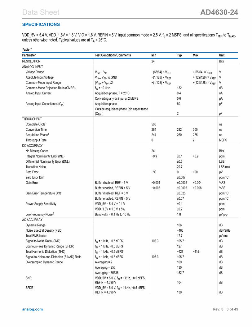
Figure 2. Voltage Levels for Timing
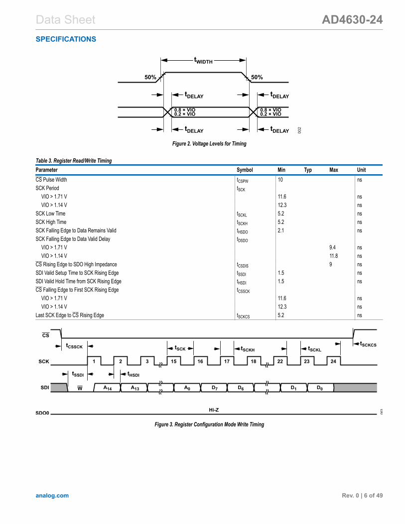
Table 3. Register Read/Write TimingParameter Symbol Min Typ Max UnitCS Pulse Width tCSPW 10 nsSCK Period tSCK
VIO > 1.71 V 11.6 nsVIO > 1.14 V 12.3 ns
SCK Low Time tSCKL 5.2 nsSCK High Time tSCKH 5.2 nsSCK Falling Edge to Data Remains Valid tHSDO 2.1 nsSCK Falling Edge to Data Valid Delay tDSDO
VIO > 1.71 V 9.4 nsVIO > 1.14 V 11.8 ns
CS Rising Edge to SDO High Impedance tCSDIS 9 nsSDI Valid Setup Time to SCK Rising Edge tSSDI 1.5 nsSDI Valid Hold Time from SCK Rising Edge tHSDI 1.5 nsCS Falling Edge to First SCK Rising Edge tCSSCK
VIO > 1.71 V 11.6 nsVIO > 1.14 V 12.3 ns
Last SCK Edge to CS Rising Edge tSCKCS 5.2 ns
Figure 3. Register Configuration Mode Write Timing

Data Sheet AD4630-24SPECIFICATIONS
analog.com Rev. 0 | 7 of 49
Figure 4. Register Configuration Mode Read Timing
Figure 5. Register Configuration Mode Command Timing
Table 4. SPI Compatible Mode TimingParameter Symbol Min Typ Max UnitSCK Period tSCK
VIO > 1.71 V 9.8 nsVIO > 1.14 V 12.3 ns
SCK Low Time tSCKLVIO > 1.71 V 4.2 nsVIO > 1.14 V 5.2 ns
SCK High Time tSCKHVIO > 1.71 V 4.2 nsVIO > 1.14 V 5.2 ns
SCK Falling Edge to Data Remains Valid tHSDO 1.4 nsSCK Falling Edge to Data Valid Delay tDSDO
VIO > 1.71 V 5.6 nsVIO > 1.14 V 8.1 ns
CS Falling Edge to SDO Valid tCSEN nsVIO > 1.71 V 6.8 nsVIO > 1.14 V 9.3 ns
CS Falling Edge to First SCK Rising Edge tCSSCKVIO > 1.71 V 9.8 nsVIO > 1.14 V 12.3 ns
Last SCK Edge to CS Rising Edge tSCKCS 4.2 nsCS Rising Edge to SDO High Impedance tCSDIS 9 nsCS Falling Edge to BUSY Rising Edge tCSBUSY 6 ns
Data Sheet AD4630-24SPECIFICATIONS
analog.com Rev. 0 | 8 of 49
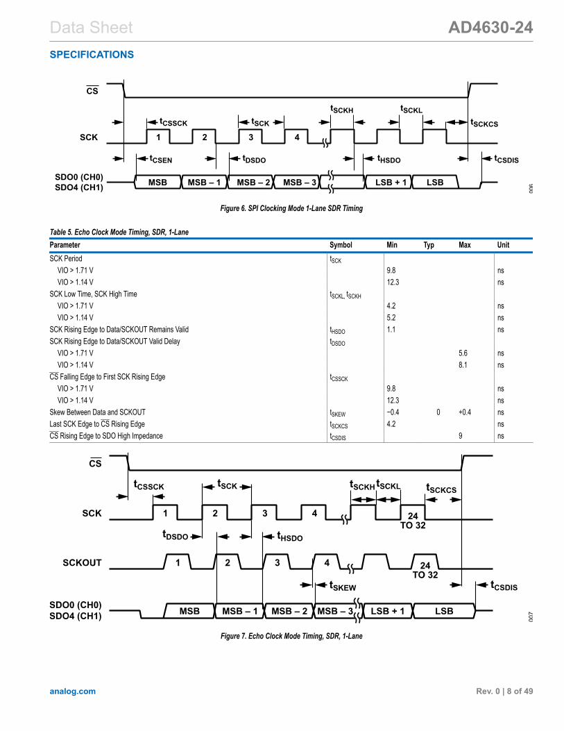
Figure 6. SPI Clocking Mode 1-Lane SDR Timing
Table 5. Echo Clock Mode Timing, SDR, 1-LaneParameter Symbol Min Typ Max UnitSCK Period tSCK
VIO > 1.71 V 9.8 nsVIO > 1.14 V 12.3 ns
SCK Low Time, SCK High Time tSCKL, tSCKHVIO > 1.71 V 4.2 nsVIO > 1.14 V 5.2 ns
SCK Rising Edge to Data/SCKOUT Remains Valid tHSDO 1.1 nsSCK Rising Edge to Data/SCKOUT Valid Delay tDSDO
VIO > 1.71 V 5.6 nsVIO > 1.14 V 8.1 ns
CS Falling Edge to First SCK Rising Edge tCSSCKVIO > 1.71 V 9.8 nsVIO > 1.14 V 12.3 ns
Skew Between Data and SCKOUT tSKEW −0.4 0 +0.4 nsLast SCK Edge to CS Rising Edge tSCKCS 4.2 nsCS Rising Edge to SDO High Impedance tCSDIS 9 ns
Figure 7. Echo Clock Mode Timing, SDR, 1-Lane

Data Sheet AD4630-24SPECIFICATIONS
analog.com Rev. 0 | 9 of 49
Table 6. Echo Clock Mode Timing, DDR, 1-LaneParameter Symbol Min Typ Max UnitSCK Period tSCK 12.3 nsSCK Low Time, SCK High Time tSCKL, tSCKH 5.2 nsSCK Edge to Data/SCKOUT Remains Valid tHSDO 1.1 nsSCK Edge to Data/SCKOUT Valid Delay tDSDO
VIO > 1.71 V 6.2 nsVIO > 1.14 V 8.7 ns
CS Falling Edge to First SCK Rising Edge tCSSCK 12.3 nsSkew Between Data and SCKOUT tSKEW −0.4 0 +0.4 nsLast SCK Edge to CS Rising Edge tSCKCS 9 nsCS Rising Edge to SDO High Impedance tCSDIS 9 ns
Figure 8. Echo Clock Mode Timing, DDR, 1-Lane
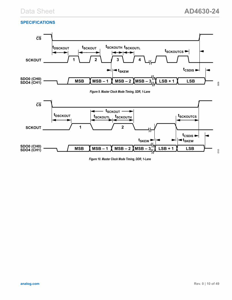
Table 7. Master Clock Mode TimingParameter Symbol Min Typ Max UnitSCK Period tSCKOUT
OSC_DIV = No Divide 11.8 12.5 13.3 nsOSC_DIV = Divide by 2 23.6 25 26.6 nsOSC_DIV = Divide by 4 47.4 50 53.2 ns
SCK Low Time tSCKOUTL 0.45 × tSCKOUT 0.55 × tSCKOUT nsSCK High Time tSCKOUTH 0.45 × tSCKOUT 0.55 × tSCKOUT nsCS Falling Edge to First SCKOUT Rising Edge tDSCKOUT
VIO > 1.71 V 10 13.6 19 nsVIO > 1.14 V 10 15 21 ns
Skew Between Data and SCKOUT tSKEW −0.4 0 +0.4 nsLast SCKOUT Edge to CS Rising Edge tSCKOUTCS 5.2 nsCS Rising Edge to SDO High Impedance tCSDIS 9 ns
Data Sheet AD4630-24SPECIFICATIONS
analog.com Rev. 0 | 10 of 49
Figure 9. Master Clock Mode Timing, SDR, 1-Lane
Figure 10. Master Clock Mode Timing, DDR, 1-Lane
Data Sheet AD4630-24ABSOLUTE MAXIMUM RATINGS
analog.com Rev. 0 | 11 of 49
Table 8.Parameter RatingAnalog Inputs
IN1+, IN1−, IN0+, IN0−, REFIN toGND
−0.3 V to VDD_5V +0.3 V
Supply VoltageVDD_5V, REF to GND −0.3 V to +6.0 VVDD_1.8V, VIO to GND −0.3 V to +2.1 V
Digital Inputs to GND −0.3 V to VIO + 0.3 VCNV to GND −0.3 V to VIO + 0.3 V
Digital Outputs to GND −0.3 V to VIO + 0.3 VStorage Temperature Range −55°C to +150°COperating Junction Temperature Range −40°C to +125°CMaximum Reflow (Package Body)Temperature
260°C
Stresses at or above those listed under Absolute Maximum Ratingsmay cause permanent damage to the product. This is a stressrating only; functional operation of the product at these or any otherconditions above those indicated in the operational section of thisspecification is not implied. Operation beyond the maximum operat-ing conditions for extended periods may affect product reliability.
THERMAL RESISTANCEThermal performance is directly linked to printed circuit board(PCB) design and operating environment. Careful attention to PCBthermal design is required.θJA is the natural convection junction to ambient thermal resistancemeasured in a one cubic foot sealed enclosure. θJC is the junctionto case thermal resistance.Table 9. Thermal ResistancePackage Type θJA θJC UnitBC-64-8 35 16 °C/W
ELECTROSTATIC DISCHARGE (ESD) RATINGSThe following ESD information is provided for handling of ESD-sen-sitive devices in an ESD protected area only.Human body model (HBM) per ANSI/ESDA/JEDEC JS-001.Field induced charged device model (FICDM) per ANSI/ESDA/JE-DEC JS-002.
ESD Ratings for AD4630-24Table 10. AD4630-24, 64-Ball CSP_BGAESD Model Withstand Threshold (kV) ClassHBM 4 3AFICDM 1.25 C3
ESD CAUTIONESD (electrostatic discharge) sensitive device. Charged devi-ces and circuit boards can discharge without detection. Althoughthis product features patented or proprietary protection circuitry,damage may occur on devices subjected to high energy ESD.Therefore, proper ESD precautions should be taken to avoid
performance degradation or loss of functionality.

Data Sheet AD4630-24PIN CONFIGURATION AND FUNCTION DESCRIPTIONS
analog.com Rev. 0 | 12 of 49
Figure 11. Pin Configuration
Table 11. Pin Function DescriptionsPin No. Mnemonic Type1 DescriptionB1 IN0+ AI Channel 0 Positive Analog Input.C1 IN0− AI Channel 0 Negative Analog Input.F1 IN1+ AI Channel 1 Positive Analog Input.G1 IN1− AI Channel 1 Negative Analog Input.A2 REFIN AI Buffered Reference Input. When using the internal reference buffer, drive REFIN with 4.096 V to 5 V
(referred to GND). To disable the reference buffer, tie REFIN to GND and drive REF with 4.096 V to 5 V.D2, D3, E2, E3 REF AI Optional Unbuffered Reference Input. Drive REF with 4.096 V to 5 V (referred to GND). This pin has a 2
μF bypass capacitor inside the package. When using the internal reference buffer, do not connect REF.D8 SDO0 DO Channel 0 Serial Data Output. The conversion result outputs on this pin. It is synchronized to SCK.C8 SDO1 DO Channel 0 Serial Data Output. The conversion result outputs on this pin. It is synchronized to SCK.D7 SDO2 DO Channel 0 Serial Data Output. The conversion result outputs on this pin. It is synchronized to SCK.C7 SDO3 DO Channel 0 Serial Data Output. The conversion result outputs on this pin. It is synchronized to SCK.F8 SDO4 DO Channel 1 Serial Data Output. The conversion result outputs on this pin. It is synchronized to SCK.G8 SDO5 DO Channel 1 Serial Data Output. The conversion result outputs on this pin. It is synchronized to SCK.F7 SDO6 DO Channel 1 Serial Data Output. The conversion result outputs on this pin. It is synchronized to SCK.G7 SDO7 DO Channel 1 Serial Data Output. The conversion result outputs on this pin. It is synchronized to SCK.H7 SCK DI Serial Data Clock Input. When the device is selected (CS = low), the conversion result is shifted out by
this clock.H6 SDI DI Serial Data Input.H5 CS DI Chip Select Input (Active Low).A6 CNV DI Convert Input. A rising edge on this input powers up the device and initiates a new conversion. This
signal must have low jitter to achieve the specified performance of the ADC. The logic levels aredetermined by VIO.
A7 RST DI Reset Input (Active Low). Asynchronous device reset.

Data Sheet AD4630-24PIN CONFIGURATION AND FUNCTION DESCRIPTIONS
analog.com Rev. 0 | 13 of 49
Table 11. Pin Function DescriptionsPin No. Mnemonic Type1 DescriptionE8 BUSY_SCKOUT DO BUSY Indicator in SPI Clocking Mode. This pin goes high at the start of a new conversion and returns
low when the conversion finishes. The logic levels are determined by VIO. When SCKOUT is enabled,this pin function is either an echo of the incoming SCK from the host controller or a clock sourced by theinternal oscillator.
A3,B3 VDD_5V P 5 V Power Supply. The range of VDD_5V depends on the reference value: 5.3 V to 5.5 V for a 5 Vreference, and 4.75 V to 5.25 V for a 4.096 V reference. This pin has a 1 μF bypass capacitor inside thepackage.
G3, H3 VDD_1.8V P 1.8 V Power Supply. The range of VDD_1.8V is 1.71 V to 1.89 V. This pin has a 1 μF bypass capacitorinside the package.
A8, B8 VIO P Input/Output Interface Digital Power. Nominally, this pin is at the same supply as the host interface (1.8V, 1.5 V, or 1.2 V). This pin has a 0.2 μF bypass capacitor inside the package. For VIO < 1.4 V, Bit IO2Xof the output driver register must be set to 1.
B6, B7, C6, D6, E6, E7, F6,G6, H8
IOGND P VIO Ground. Connect to the same ground plane as GND.
A1, D1, E1, H1, B2, C2, F2,G2, H2, C3, F3, A4, B4, C4,D4, E4, F4, G4, H4, A5, B5,C5, D5, E5, F5, G5
GND P Power Supply Ground.
1 AI is analog input, P is power, DI is digital input, and DO is digital output.

Data Sheet AD4630-24TYPICAL PERFORMANCE CHARACTERISTICS
analog.com Rev. 0 | 14 of 49
VDD_5V = 5.4 V, VDD_1.8V = 1.8 V, VIO = 1.8 V, REFIN = 5 V, input common mode = 2.5 V, fS = 2 MSPS, and all specifications TMIN to TMAX,unless otherwise noted. Typical values are at TA = 25°C.
Figure 12. INL Error vs. Output Code, Differential Input
Figure 13. INL Error vs. Output Code, Single-Ended Input
Figure 14. Code Histogram for Shorted Inputs
Figure 15. FFT, 2 MSPS, fIN = 1 kHz, VREF = 5 V
Figure 16. SNR and SINAD vs. Input Frequency
Figure 17. THD vs. Input Frequency and Amplitude

Data Sheet AD4630-24TYPICAL PERFORMANCE CHARACTERISTICS
analog.com Rev. 0 | 15 of 49
Figure 18. SNR and SINAD vs. Input Amplitude, fIN = 1 kHz
Figure 19. SNR and SINAD vs. Temperature, fIN = 1 kHz
Figure 20. THD vs. Temperature, fIN = 1 kHz
Figure 21. INL vs. Temperature
Figure 22. Zero Error and Gain Error vs. Temperature
Figure 23. Dynamic Range vs. Number of Averages

Data Sheet AD4630-24TYPICAL PERFORMANCE CHARACTERISTICS
analog.com Rev. 0 | 16 of 49
Figure 24. Low Frequency Noise (Output Data Rate = 19.5 SPS AfterAveraging Blocks of 2048 Samples)
Figure 25. Analog Input Current vs. Differential Input
Figure 26. Reference Buffer Offset Voltage vs. Temperature
Figure 27. Error During Conversion Burst After Long Idle Time
Figure 28. REFIN Current vs. Temperature
Figure 29. REF Current vs. Analog Input
Data Sheet AD4630-24TYPICAL PERFORMANCE CHARACTERISTICS
analog.com Rev. 0 | 17 of 49
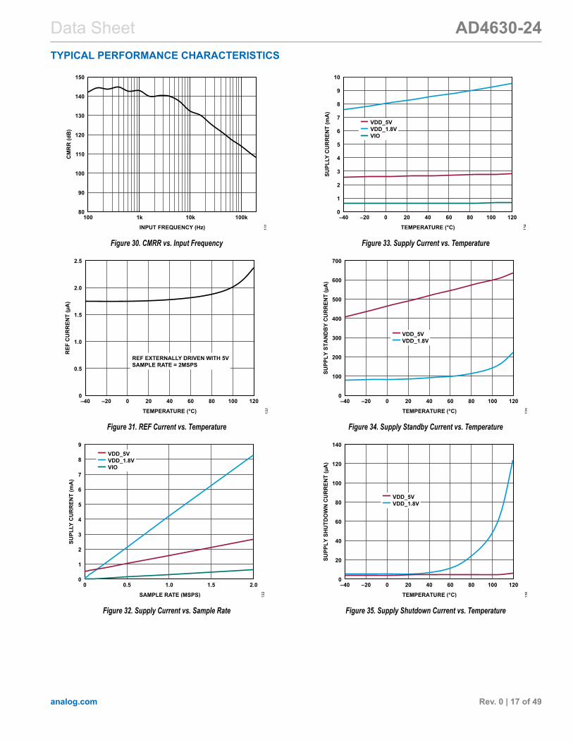
Figure 30. CMRR vs. Input Frequency
Figure 31. REF Current vs. Temperature
Figure 32. Supply Current vs. Sample Rate
Figure 33. Supply Current vs. Temperature
Figure 34. Supply Standby Current vs. Temperature
Figure 35. Supply Shutdown Current vs. Temperature

Data Sheet AD4630-24TERMINOLOGY
analog.com Rev. 0 | 18 of 49
INTEGRAL NONLINEARITY ERROR (INL)INL is the deviation of each individual code from a line drawn fromnegative full scale through positive full scale. The point used asnegative full scale occurs ½ LSB before the first code transition.Positive full scale is defined as a level 1½ LSB beyond the lastcode transition. The deviation is measured from the middle of eachcode to the true straight line (see Figure 37).
DIFFERENTIAL NONLINEARITY ERROR (DNL)In an ideal ADC, code transitions are 1 LSB apart. DNL is themaximum deviation from this ideal value. DNL is often specified interms of resolution for which no missing codes are guaranteed.
ZERO ERROR (ZE)Zero error is the difference between the ideal midscale voltage, 0 V,and the actual voltage producing the midscale output code, 0 LSB.
GAIN ERROR (GE)The first transition (from 100 ... 00 to 100 ... 01) occurs at a level ½LSB above nominal negative full scale. The last transition (from 011… 10 to 011 … 11) occurs for an analog voltage 1½ LSB below thenominal full scale. The gain error is the deviation of the differencebetween the actual level of the last transition and the actual level ofthe first transition from the difference between the ideal levels.
SPURIOUS-FREE DYNAMIC RANGE (SFDR)SFDR is the difference, in decibels (dB), between the rms amplitudeof a full-scale input signal and the peak spurious signal.
EFFECTIVE NUMBER OF BITS (ENOB)ENOB is a measurement of the resolution with a sine wave input.ENOB is related to SINAD as follows: ENOB = (SINAD dB − 1.76)/6.02. ENOB is expressed in bits.
TOTAL HARMONIC DISTORTION (THD)THD is the ratio of the rms sum of the first five harmonic compo-nents to the rms value of a full-scale input signal and is expressedin decibels.
DYNAMIC RANGE (DR)Dynamic range is the rms voltage of a full-scale sine wave to thetotal rms voltage of the noise measured. The value for dynamicrange is expressed in decibels. Dynamic range is measured with asignal at −60 dBFS so that it includes all noise sources and DNLartifacts.
SIGNAL-TO-NOISE RATIO (SNR)SNR is the ratio of the rms voltage of a full-scale sine wave tothe rms sum of all other spectral components below the Nyquistfrequency, excluding harmonics and dc. The value for SNR isexpressed in decibels.
SIGNAL-TO-NOISE-AND-DISTORTION (SINAD)RATIOSINAD is the ratio of the rms voltage of a full-scale sine wave tothe rms sum of all other spectral components that are less than theNyquist frequency, including harmonics but excluding dc. The valueof SINAD is expressed in decibels.
APERTURE DELAYAperture delay is the measure of the acquisition performance andis the time between the rising edge of the CNV input and when theinput signal is held for a conversion.
TRANSIENT RESPONSETransient response is the time required for the ADC to acquire afull-scale input step to ±1 LSB accuracy.
COMMON-MODE REJECTION RATIO (CMRR)CMRR is the ratio of the power in the ADC output at the frequency,f, to the power of a 4.5 V p-p sine wave applied to the inputcommon-mode voltage of frequency, f.CMRR dB = 10 × log PADC_IN PADC_OUTwhere:PADC_IN is the common-mode power at the frequency, f, applied tothe inputs.PADC_OUT is the power at the frequency, f, in the ADC output.
POWER SUPPLY REJECTION RATIO (PSRR)PSRR is the ratio of the power in the ADC output at the frequency,f, to the power of a 200 mV p-p sine wave applied to the ADC VDDsupply of frequency, f.PSRR dB = 10 × log PVDD_IN PADC_OUTwhere:PVDD_IN is the power at the frequency, f, at the VDD pin.PADC_OUT is the power at the frequency, f, in the ADC output.

Data Sheet AD4630-24THEORY OF OPERATION
analog.com Rev. 0 | 19 of 49
Figure 36 shows the basic functions of the AD4630-24.
Figure 36. Functional Block Diagram and Channel Architecture
OVERVIEWThe AD4630-24 is a low noise, low power, high speed, dual 24-bitSAR ADC. The AD4630-24 is capable of converting 2,000,000samples per second (2 MSPS). The AD4630-24 offers severalanalog and digital features to ease system design. The analogfeatures include a wide common-mode range, which eases levelshifting requirements, as well as an extended fully differential inputrange of ±(65/64) × VREF, which eases the margin requirements onsignal conditioning.The AD4630-24 has an integrated reference buffer with an integrat-ed decoupling capacitor to minimize the external components onboard. The on-chip track-and-hold circuitry does not exhibit anypipeline delay or latency, making it ideal for control loops and high
speed applications. The digital features include offset correction,gain adjustment, and averaging, which offload the host processor.The user can configure the device for one of several output codeformats (see the Summary of Selectable Output Data Formatssection).The AD4630-24 uses a Flexi-SPI allowing the data to be accessedvia multiple SPI lanes, which relaxes clocking requirements for thehost SPI controller. An echo clock mode is also available to assistin data clocking, simplifying the use of isolated data interfaces. TheAD4630-24 has a valid first conversion after exiting power-downmode. The AD4630-24 achieves ±0.9 ppm INL maximum, with nomissing codes at 24 bits, and 105.7 dB SNR at 2 MSPS. TheAD4630-24 dissipates only 15 mW per channel at 2 MSPS.
Data Sheet AD4630-24THEORY OF OPERATION
analog.com Rev. 0 | 20 of 49
CONVERTER OPERATIONThe AD4630-24 operates in two phases: acquisition phase andconversion phase. In the acquisition phase, the internal track-and-hold circuitry is connected to each input pin (INX+, INX-) andsamples the voltage on each pin independently. Issuing a risingedge pulse on the CNV pin initiates a conversion. The rising edgepulse on the CNV pin also asserts the BUSY signal to indicate aconversion in progress. At the end of conversion, the BUSY signalde-asserts. The conversion result is a 24-bit code representing theinput voltage difference and an 8-bit code representing the inputcommon-mode voltage. Depending on the device configuration, thisconversion result can be processed digitally and latched into theoutput register. The acquisition circuit on each input pin is alsoprecharged to the previous sample voltage, which minimizes thekickback charge to the input driver. The host processor retrieves theoutput code via the SDO pins that are internally connected to theoutput register.
TRANSFER FUNCTIONIn the default configuration, the AD4630-24 digitizes the full-scaledifference voltage of 2 × VREF into 224 levels, resulting in an LSBsize of 0.596 µV with VREF = 5 V. Note that 1 LSB at 24 bitsis approximately 0.06 ppm. The ideal transfer function is shownin Figure 37. The differential output data is in twos complementformat. Table 12 summarizes the mapping of input voltages todifferential output codes.
Figure 37. ADC Ideal Transfer Function for the Differential Output Codes(FSR Is Full-Scale Range)
Table 12. Input Voltage to Output Code Mapping
DescriptionAnalog Input VoltageDifference
Digital Output Code (TwosComplement, Hex)
FSR − 1 LSB (8388607 × VREF)/(8388608) 0x7FFFFFMidscale + 1 LSB VREF/(8388608) 0x000001Midscale 0 V 0x000000Midscale − 1 LSB −VREF/(8388608) 0xFFFFFF
Table 12. Input Voltage to Output Code Mapping
DescriptionAnalog Input VoltageDifference
Digital Output Code (TwosComplement, Hex)
−FSR + 1 LSB −(8388607 × VREF)/(8388608) 0x800001−FSR −VREF 0x800000
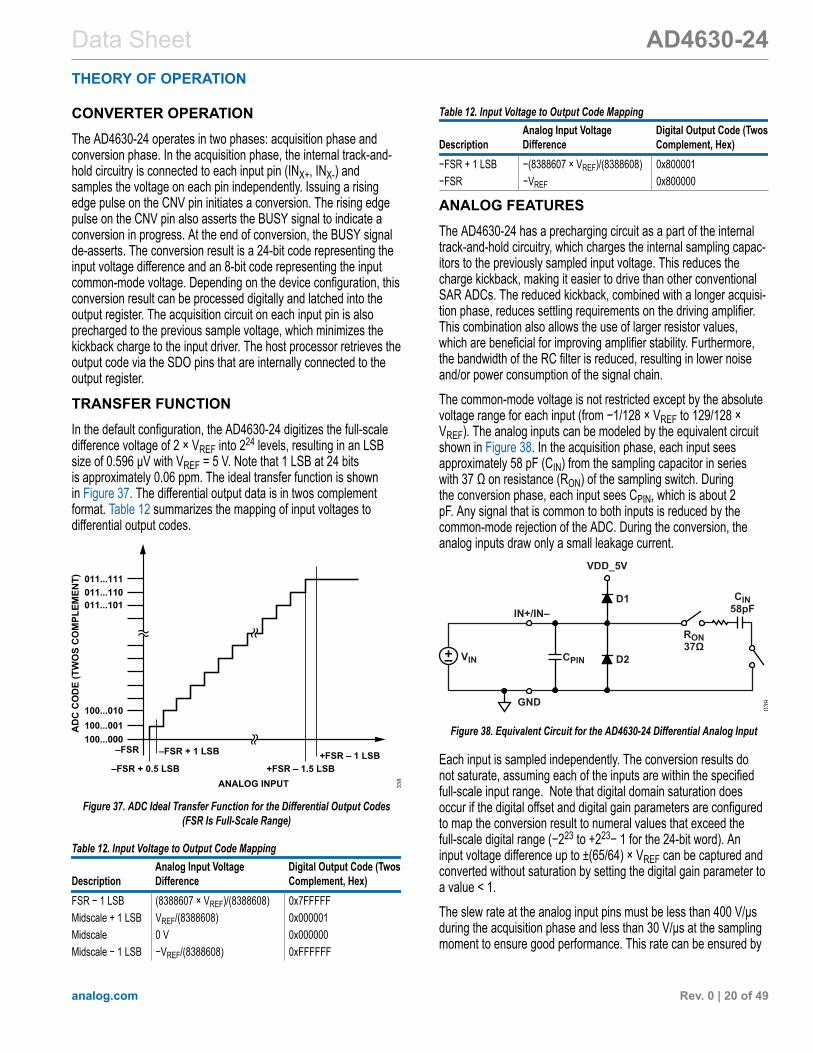
ANALOG FEATURESThe AD4630-24 has a precharging circuit as a part of the internaltrack-and-hold circuitry, which charges the internal sampling capac-itors to the previously sampled input voltage. This reduces thecharge kickback, making it easier to drive than other conventionalSAR ADCs. The reduced kickback, combined with a longer acquisi-tion phase, reduces settling requirements on the driving amplifier.This combination also allows the use of larger resistor values,which are beneficial for improving amplifier stability. Furthermore,the bandwidth of the RC filter is reduced, resulting in lower noiseand/or power consumption of the signal chain.The common-mode voltage is not restricted except by the absolutevoltage range for each input (from −1/128 × VREF to 129/128 ×VREF). The analog inputs can be modeled by the equivalent circuitshown in Figure 38. In the acquisition phase, each input seesapproximately 58 pF (CIN) from the sampling capacitor in serieswith 37 Ω on resistance (RON) of the sampling switch. Duringthe conversion phase, each input sees CPIN, which is about 2pF. Any signal that is common to both inputs is reduced by thecommon-mode rejection of the ADC. During the conversion, theanalog inputs draw only a small leakage current.
Figure 38. Equivalent Circuit for the AD4630-24 Differential Analog Input
Each input is sampled independently. The conversion results donot saturate, assuming each of the inputs are within the specifiedfull-scale input range. Note that digital domain saturation doesoccur if the digital offset and digital gain parameters are configuredto map the conversion result to numeral values that exceed thefull-scale digital range (−223 to +223− 1 for the 24-bit word). Aninput voltage difference up to ±(65/64) × VREF can be captured andconverted without saturation by setting the digital gain parameter toa value < 1.The slew rate at the analog input pins must be less than 400 V/µsduring the acquisition phase and less than 30 V/µs at the samplingmoment to ensure good performance. This rate can be ensured by

Data Sheet AD4630-24THEORY OF OPERATION
analog.com Rev. 0 | 21 of 49
choosing values for the external RC circuit such that the RC timeconstant is more than 12.5 ns (R × C > 12.5e-9).
DIGITAL SAMPLE PROCESSING FEATURESThe AD4630-24 supports several digital and data processing fea-tures that can be applied to the signal samples. These features aredescribed in this section. These features are enabled and disabledvia the control registers of the AD4630-24. Figure 36 contains anADC channel architecture block diagram illustrating the digital anddata processing features available for each input channel.
Full-Scale SaturationThe conversion results saturate digitally (before any postprocess-ing) when either or both inputs exceed the specified analog limits.After applying offset and gain scaling, the results are truncatedto 24-bit representation (saturating at maximum 0x7FFFFF andminimum 0x800000). Take care to avoid unintentional saturation,especially when applying digital offset and/or gain scaling. See theDigital Offset Adjust and Digital Gain sections for more details onthe use of these features.
Common-Mode OutputWhen the host controller writes 0x1 or 0x2 to the OUT_DATA_MDbit field of the modes register (see the Modes Register section),an 8-bit code representing the input common-mode voltage isappended to the 16-bit or 24-bit code representing the input voltagedifference. The LSB size of the 8-bit code is VREF/256. The 8-bitcode saturates at 0 and 255 when the common-mode input voltageis 0 V and VREF, respectively. The 8-bit code is not affected bydigital offset and gain scaling, which is applied only to the coderepresenting the input voltage difference.
Block AveragingThe AD4630-24 provides a block averaging filter (SINC1) withprogrammable block length 2N, where N = 1, 2, 3, …, 16. The filteris reset after processing each block of 2N samples. The filter isenabled by writing 0x3 to the OUT_DATA_MD bit field of the modesregister (see the Modes Register section) as well as a value (1 ≤N ≤ 16) to the AVG_VAL bit field in the averaging mode register(see the Averaging Mode Register section). In this configuration,the output sample word is 32 bits. The 30 MSBs represent thenumerical value of the 24-bit codes averaged in blocks of 2N
samples. Scaling is such that the 24 MSBs of the 30-bit codeare equal to the 24-bit codes when averaging blocks of constantvalues. The 31st bit (OR) is an overrange warning bit, which is highwhen one or more samples in the block are subject to saturation.The 32nd bit (SYNC) is high once every 2N conversion cycles toindicate when the average values are updated at the end of eachblock of samples. See the Summary of Selectable Output DataFormats section for an illustration of the data format when the filteris enabled.
The effective data rate in averaging mode is FCNV/2N. The resetvalue of N in the AVG_VAL bit field is 0x00 (no averaging). Figure53 shows an example timing diagram in averaging mode. Figure 39shows the frequency response of the filter for N = 1, 2, 3, 4, and 5.
Figure 39. Frequency Response Examples for the Block Averaging Filter
Digital Offset AdjustEach ADC channel can be independently programmed to add a24-bit signed offset value to the sample data (see the RegisterDetails section). When adding an offset to the samples, it is possi-ble to cause the sample data to saturate numerically. Take thisinto account when using the offset feature. The default value is0x000000. See the Channel 0 Offset Registers section or Channel1 Offset Registers section in the AD4630-24 register map for moredetails.
Digital GainEach ADC channel can be independently programmed to applya 16-bit unsigned digital gain (CHx_USER_GAIN) to the digitalsamples (see the Register Details section). The gain is applied toeach sample based on the following equation:CodeOUT = CodeIN × (CHx_USER_GAIN/0x8000)where: 0x0000 < CHx_USER_GAIN < 0xFFFF.The effective gain range is 0 to 1.99997. Note that applying gain tothe samples can cause numerical saturation. The default value is0x8000 (gain = 1). To measure input voltage differences exceeding(±VREF), set the gain below unity to avoid the numerical saturationof the 24-bit/16-bit/30-bit output differential codes. See the Channel0 Gain Registers section or Channel 1 Gain Registers section in theAD4630-24 register map for more details.
Test PatternTo facilitate functional testing and debugging of the SPI, the hostcontroller can write a 32-bit test pattern to the AD4630-24 (see the

Data Sheet AD4630-24THEORY OF OPERATION
analog.com Rev. 0 | 22 of 49
Test Pattern Registers section). The value written to the test patternregisters applies to both ADC channels, and is output using thenormal sample cycle timing on each channel. The 32-bit test patternoutput mode is enabled by writing 0x4 to the OUT_DATA_MD bitfield of the modes register (see the Modes Register section). Thedefault value stored in the test pattern registers is 0x5A5A0F0F.
Summary of Selectable Output Data FormatsFigure 40 summarizes the output data formats that are available onthe AD4630-24, which are selected in the modes register (see theModes Register section). Note that the selected mode is applied toboth channels. The OR and SYNC flags are each 1 bit.
Figure 40. Summary of Selectable Output Sample Formats
Data Sheet AD4630-24APPLICATIONS INFORMATION
analog.com Rev. 0 | 23 of 49
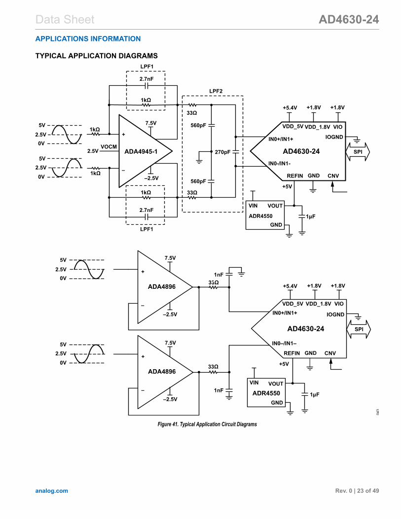
TYPICAL APPLICATION DIAGRAMS
Figure 41. Typical Application Circuit Diagrams
Data Sheet AD4630-24APPLICATIONS INFORMATION
analog.com Rev. 0 | 24 of 49
ANALOG FRONT-END DESIGN
Driver Amplifier ChoiceFigure 41 shows two examples for driving the AD4630-24. Eitheramplifier can be combined with an upstream stage that providesadditional signal conditioning. Both amplifiers can accommodatesingle-ended or differential inputs. To take advantage of the excel-lent SNR and THD performance of the AD4630-24, choose a driveramplifier that has low noise and THD sufficient to meet the applica-tion requirements. In addition to the amplifiers shown in Figure 41,the LTC6227 is another driver option. Analog Devices, Inc., offersseveral companion driver amplifiers that can be found on the ADCdrivers web page.
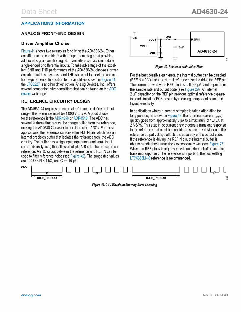
REFERENCE CIRCUITRY DESIGNThe AD4630-24 requires an external reference to define its inputrange. This reference must be 4.096 V to 5 V. A good choicefor the reference is the ADR4550 or ADR4540. The ADC hasseveral features that reduce the charge pulled from the reference,making the AD4630-24 easier to use than other ADCs. For mostapplications, the reference can drive the REFIN pin, which has aninternal precision buffer that isolates the reference from the ADCcircuitry. The buffer has a high input impedance and small inputcurrent (5 nA typical) that allows multiple ADCs to share a commonreference. An RC circuit between the reference and REFIN can beused to filter reference noise (see Figure 42). The suggested valuesare 100 Ω < R < 1 kΩ, and C >= 10 μF.
Figure 42. Reference with Noise Filter
For the best possible gain error, the internal buffer can be disabled(REFIN = 0 V) and an external reference used to drive the REF pin.The current drawn by the REF pin is small (<2 μA) and depends onthe sample rate and output code (see Figure 29). An internal2 μF capacitor on the REF pin provides optimal reference bypass-ing and simplifies PCB design by reducing component count andlayout sensitivity.In applications where a burst of samples is taken after idling forlong periods, as shown in Figure 43, the reference current (IREF)quickly goes from approximately 0 µA to a maximum of 1.8 µA at2 MSPS. This step in dc current draw triggers a transient responsein the reference that must be considered since any deviation in thereference output voltage affects the accuracy of the output code.If the reference is driving the REFIN pin, the internal buffer isable to handle these transitions exceptionally well (see Figure 27).When the REF pin is being driven with no external buffer, and thetransient response of the reference is important, the fast settlingLTC6655LN-5 reference is recommended.
Figure 43. CNV Waveform Showing Burst Sampling

Data Sheet AD4630-24APPLICATIONS INFORMATION
analog.com Rev. 0 | 25 of 49
DEVICE RESETThe AD4630-24 provides two options for performing a device resetusing the serial interface. A hardware reset is initiated by pulsingthe voltage on the RST pin low. A software reset is initiated bysetting both the SW_RESET and SW_RESETX bits in the InterfaceConfiguration A register to 1 in the same write instruction (see theInterface Configuration A Register section).Performing a hardware or software reset asserts the RESET_OC-CURRED bit in the digital diagnostics register (see the DigitalDiagnostics Register section). The RESET_ OCCURRED bit iscleared by writing it with a 1. RESET_ OCCURRED can be used bythe digital host to confirm the AD4630-24 executed a device reset.The AD4630-24 is designed to generate a power-on reset (POR)when VDD_5V and VDD_1.8V are first applied. A POR resets thestate of the user configuration registers and asserts the RESET_OCCURRED bit. If VDD_5V or VDD_1.8V drops below its specifiedoperating range, a POR occurs. Perform a hardware or softwarereset after a POR.Figure 44 shows the timing diagram for performing a device resetusing the RST input. The minimum RST pulse width is 50 ns,represented by tRESETPW in Figure 44 and Table 1. Perform a resetno sooner than 3 ms after the power supplies are valid and stable(this delay is represented by tRESET_DELAY in Figure 44 and Table 1).After a hardware or software reset, no SPI commands or conver-sions can be started for 750 µs.
Figure 44. Power-On Reset (POR) Timing
POWER SUPPLIESThe AD4630-24 does not have any specific power supply sequenc-ing requirements. Take care to adhere to the maximum voltagerelationships described in the Absolute Maximum Ratings section.The voltage range for the VDD_5V supply depends on the chosenreference voltage (see the internal reference buffer parameter orexternally overdriven reference parameter in Table 1). Figure 45shows the minimum and maximum values for VDD_5V with respectto REFIN and REF. VDD_5V voltage values above the maximumor below the minimum result in either damage to the device ordegraded performance.
Figure 45. VDD_5V Minimum and Maximum Values for REFIN/REF
The AD4630-24 has a POR circuit that resets the AD4630-24 atinitial power-up or whenever VDD_5V or VDD_1.8V drops below itsspecified operating range.Note that the VDD_5V and the VDD_1.8V supplies have internal1 µF bypass capacitors inside the package, whereas VIO hasan internal 0.2 µF bypass capacitor. These internal capacitorsreduce the bill of materials (BOM) count and solution size. If thebulk supply bypass capacitors are not close to the ADC, externalcapacitors can be added next to the ADC. The minimum rise timefor all supplies is 100 µs.
Power Consumption StatesDuring a conversion, the power consumption rate of the AD4630-24is at its highest. When the conversion completes, the AD4630-24enters a standby state and much of the internal circuitry is powereddown, and current consumption drops to less than 20% relativeto the conversion state. To ensure full accuracy, some circuitry,including the reference buffer, remains powered on during thestandby state.The device can be placed into a lower power shutdown stateduring periods when the convert clock is idle by writing 0x3 to theOPERATING_MODES bit field of the device configuration register(see the Device Configuration Register section). The default valueof this bit field is 00 for normal operating mode. In the shutdownstate, the current consumption typically drops to less than 10 µA.
Shutdown ModeWhen the user enters shutdown mode, the internal reference bufferis disabled and a 500 Ω switch connects REFIN to REF (unlessREFIN is grounded and REF is externally driven). This functionalitykeeps the 2 µF capacitor on REF charged up to allow fast recoverywhen the user leaves shutdown mode. Because of this keep aliveswitch, some charge is injected to REFIN when the user entersshutdown mode (400 pC) and leaves shutdown mode (5 pC). Whenleaving shutdown mode, REF is accurate after 30 µs.

Data Sheet AD4630-24SERIAL INTERFACE
analog.com Rev. 0 | 26 of 49
The AD4630-24 supports a multilane SPI for each channel, witha common bit clock (SCK). The flexible VIO supply allows theAD4630-24 to communicate with any digital logic operating be-tween 1.2 V and 1.8 V. However, for VIO levels below 1.4 V, theIO2X bit in the output driver register must be set to 1 (see theOutput Driver Register section). The serial output data is clockedout on up to 4 SDO lanes per channel (see Figure 46). An echoclock mode that is synchronous with the output data is availableto ease timing requirements when using isolation on the digitalinterface. A master clock mode is also available and uses aninternal oscillator to clock out the data bits. The SPI Signals sectiondescribes the operation of the AD4630-24 SPI.
Figure 46. AD4630-24 Multilane SPI
SPI SIGNALSThe SPI is a multilane interface that is used to both configure theADC as well as retrieve sampled data. The SPI consists of thefollowing signals: CS (input). Chip select. CS must be set low to initiate/enable a
data transfer to or from the SDI and SDOx pins of the ADC. CStiming for reading sample data can be moderated by observingthe state of the BUSY pin. For echo clock mode and masterclock mode, CS timing must be controlled by the host processorbecause the BUSY pin is used as the bit clock output for theseclocking modes.
SDI (input). Serial data input stream from the host controller toADC. SDI is only used when writing data into one of the userregisters of the AD4630-24.
CNV (input). The CNV signal is sourced by the host controllerand initiates a sample conversion. The frequency of the CNVsignal determines the sampling rate of the AD4630-24. Themaximum frequency of the CNV clock is 2 MSPS.
SCK (input). Serial data clock sourced by the host controller. Themaximum supported SCK rate for output data transfer is 100MHz. For register reads and writes, the maximum SCK rate is 86MHz for VIO > 1.71 V, and 81 MHz for 1.14 V < VIO < 1.71 V.
SDO0 through SDO7 (outputs). Data lanes to the host controller.Lanes SDO0 to SDO3 are allocated to ADC Channel 0, whereaslanes SDO4 to SDO7 are allocated to ADC Channel 1. Thenumber of data lanes configured for each channel can be either1, 2, or 4 lanes (see the output data modes in the Table 14section). The number of data lanes is configured in the modesregister. Note that the selected number of data lanes is appliedto both ADC channels. The channels cannot be independentlyconfigured.
BUSY_SCKOUT (output). The behavior of the BUSY_SCKOUTpin is dependent on selected clocking mode. Table 13 defines itsbehavior for each clocking mode.
Table 13. BUSY_SCKOUT Pin Behavior vs. Clocking ModeClocking Mode BehaviorSPI Clocking Mode Valid BUSY signal for the ADC conversion status. BUSY
goes high when a conversion is triggered by the CNVsignal. BUSY goes low when the conversion completes.
Echo Clock Mode Bit clock. BUSY_SCKOUT is a delayed version of SCKinput.
Master Clock Mode Bit clock. BUSY_SCKOUT sources the clock from theinternal oscillator.
Register Access ModeThe AD4630-24 offers programmable user registers to configure thedevice as outlined in the Registers section. By default, at power-up,the device is in conversion mode. Therefore, to access the userregisters, a special access command must be sent by the hostcontroller over the SPI, as shown in Figure 5. When this registeraccess command is sent over the SPI, the device enters theregister configuration mode. To read back the values from one ofthe user registers listed in the Registers section, the host controllermust send the pattern shown in Figure 4. To write to one of theuser registers, the host controller must send the pattern shown inFigure 3. In either case (read/write), the host controller must alwaysissue 24 clock pulses on the SCK line and pull CS low for the entiretransaction.After writing to or reading from the appropriate user registers,the host controller must exit the register configuration mode bywriting 0x01 to Register Address 0x0014 as detailed in the exitconfiguration mode register. An algorithm for register read/writeaccess is as follows:1. Perform a readback from dummy Register Address 0x3FFF to
enter the register configuration mode.2. Readback from or write to the desired user register addresses.3. Exit the register configuration mode by writing 0x01 to Register
Address 0x0014. Exiting register configuration mode causes theregister updates to take effect.
Stream ModeThe AD4630-24 also offers a way to perform bulk register read/writetransactions while the AD4630-24 is in register configuration mode.

Data Sheet AD4630-24SERIAL INTERFACE
analog.com Rev. 0 | 27 of 49
To perform bulk read/write registers transactions, keep CS low andissue SCK pulses in multiples of 8 because each register is onlyone byte (8 bits) wide. In stream mode, only address decrementingis allowed, meaning that the user can read back from or write tothe initial register address and register addresses that are directlybelow the initial register address. Apply register accesses in streammode to register blocks with contiguous addresses. However, it ispossible to address registers that are not present in the register
map. To do so, write all zeros to these registers, or, when readingback, discard the contents read from these registers because itis random data. See the Registers section to see which registeraddress is valid and continuous. For example, to read back a 24-bitoffset value in one shot, the user must issue 24 SCK pulses staringfrom Register Address 0x0018. Figure 47 shows the timing diagramfor a bulk read starting at a given address.
Figure 47. Stream Mode Bulk Register Read Back Operation

Data Sheet AD4630-24SERIAL INTERFACE
analog.com Rev. 0 | 28 of 49
SAMPLE CONVERSION TIMING AND DATATRANSFERA conversion starts on the rising edge of the CNV signal, as shownin Figure 48. Once the conversion completes, CS can be asserted,which causes the current conversion result to load into the outputshift register.Referring to Figure 48, there are two optional data transfer zonesfor Sample N. Zone 1 represents the use case where CS isasserted immediately following the de-assertion of the BUSY signalfor the Sample N conversion (in SPI conversion mode), or after 300ns for echo and master clock modes. For Zone 1, the available timeto read out Sample N is given by:Zone 1 data read window= tCYC− tCONV− tQUIET_CNV_ADVFor example, if FCNV is 2 MSPS (tCYC = 500 ns) and the typicalvalue of tCONV (282 ns) is used, the available window width is 198.4ns (= 500 ns – 282 ns – 19.6 ns).Zone 2 represents the case where an assertion of CS to readSample N is delayed until after the conversion for Sample N+1initiates.
To prevent data corruption, a quiet zone must be observed beforeand after each rising edge of the CNV signal, as shown in Figure48. The quiet zone immediately before the rising edge of CNV is la-beled as tQUIET_CNV_ADV, and is equal to 19.6 ns. The quiet zone im-mediately after the rising edge of CNV is labeled tQUIET_CNV_DELAY,and is equal to 9.8 ns. Assuming that the CS asserts immediatelyafter the quiet zone around the rising edge of CNV, the amount oftime available to clock out the data is:Zone 2 data read window= tCYC− tQUIET_CNV_DELAY− tQUIET_CNV_ADVFor example, if FCNV is 2 MSPS (tCYC = 500 ns) and the typicalvalue of tCONV (282 ns) is used, the available window width is 470.6ns (= 500 ns – 9.8 ns – 19.6 ns). The Zone 2 transfer windowis longer than the Zone 1 window, which can enable the use ofa slower SCK on the SPI and ease the timing requirements forthe interface. When using Zone 2 for the data transfer, assert CSimmediately after the quiet zone. CS must be asserted at least 25ns before the falling edge of BUSY for Sample N+1. If not, SampleN is overwritten with Sample N+1.
Figure 48. Example Timing for Data Transfer Zones

Data Sheet AD4630-24SERIAL INTERFACE
analog.com Rev. 0 | 29 of 49
CLOCKING MODESThis section covers the various clocking modes supported by theAD4630-24 SPI. These modes are available for 1-lane, 2-lane,4-lane, and interleaved configurations. The clocking mode is config-ured in the modes register (see Table 16 for register descriptions).Note that the selected clocking mode applies to both ADC chan-nels. The channels cannot be independently configured.
SPI Clocking ModeSPI clocking mode is the default clocking mode of the AD4630-24and is equivalent to a host sourced bit clock (SCK), in which thehost controller uses its own clock to latch the output data. The SPI
compatible clocking mode is enabled by writing 0x0 to the CLK_MDbit field of the modes register (see the Modes Register section).The interface connection is as shown in Figure 46. In this mode, theBUSY signal is valid and indicates the completion of a conversion(high to low transition of BUSY). A simplified sample cycle is shownin Figure 49. When not in averaging mode, if the host controllerdoes not use the BUSY signal to detect the completion of aconversion, and instead uses an internal timer to retrieve the data,the host controller must wait at least 300 ns after the rising edgeof the CNV pulse before asserting CS low. When operating in blockaveraging mode, the host controller must assert CS low no soonerthan 300 ns after the rising edge of the CNV pulse for the lastsample in the block.
Figure 49. Typical Sample Cycle for SPI Clocking Mode

Data Sheet AD4630-24SERIAL INTERFACE
analog.com Rev. 0 | 30 of 49
Echo Clock ModeFigure 50 shows the signal connections for the echo clock mode.The echo clock mode is enabled by writing 0x1 to the CLK_MDbit field of the modes register (see the Modes Register section).In this mode, the BUSY_SCKOUT pin cannot be used to detecta conversion completion. The BUSY_SCKOUT pin becomes a bitclock output and is sourced by looping through the SCK of the hostcontroller to the BUSY_SCKOUT pin (with some fixed delay, 5.4 nsto 7.9 ns, depending on VIO). To begin retrieving the conversiondata in nonaveraging mode, the host controller must assert CS lowno sooner than 300 ns after the rising edge of the CNV pulse.When the ADC is configured for block averaging mode, the hostcontroller must assert CS low no sooner than 300 ns after the risingedge of the CNV pulse for the last sample in the block. Exampletiming diagrams are shown in the Data Clocking Requirements andTiming section. When echo clock mode is enabled, SCKOUT isaligned with SDOx transitions, making the data and clock timinginsensitive to asymmetric propagation delays in the SDO and SCKpaths.
Figure 50. Echo Clock Mode Signal Path Diagram
Master Clock ModeWhen enabled, master clock mode uses the internal oscillator asthe bit clock source. The master clock mode is enabled by writing0x2 to the CLK_MD bit field of the modes register. The bit clockfrequency can be programmed in the OSC_DIV bit field in theinternal oscillator register, with available divisor values of 1, 2, or 4(see the Internal Oscillator Register section). Figure 51 shows thesignal connections for the master clock mode. In this mode, theBUSY_SCKOUT pin provides the bit clock output and cannot beused to detect a conversion completion. The AD4630-24 automati-cally calculates the number of clock pulses required to clock outthe conversion data based on word size, number of active lanes,and choice of single data rate or DDR mode. The number of clockpulses can be read from the OSC_LIMIT bit field of the internaloscillator register. The SCK from the host must not be active. Whenretrieving the conversion data in nonaveraging mode, the host mustnot assert CS low sooner than 300 ns after the rising edge of theCNV pulse. When the ADC is configured in averaging mode for 2N
averages, the host must not assert CS low sooner than 300 ns afterthe rising edge of CNV pulse for the last sample in the block.
Figure 51. Master Clock Mode Signal Path Example
Single Data RateSingle data rate clocking (SDR) in which one bit (per active lane)is clocked out during a single clock cycle, is supported for alloutput configurations and sample formats (see Table 14). The SDRclocking mode is enabled by default at power-up or can be enabledby writing 0 to the DDR_MD bit of the modes register (see theModes Register section).
Dual Data RateDDR mode (two data bit transitions per clock cycle per active lane)is available only for master clock mode and echo clock mode.Note that the selected data rate mode is applied to both ADC chan-nels. DDR clocking mode is enabled by writing 1 to the DDR_MDbit of the modes register (see the Modes Register section). DDRmode uses half the number of SCK pulses to clock out conversiondata in comparison to SDR mode.
1-Lane Output Data Clocking Mode1-lane output data clocking mode is the default output data clockingmode at power-up. 1-lane output data clocking mode is enabledby writing 0x0 to the LANE_MD bit of the modes register (seethe Modes Register section). The active lane for ADC Channel 0is SDO0. The active lane for ADC Channel 1 is SDO4. Exampletiming diagrams for 1-lane output data clocking mode using SPIclocking mode, echo clock mode, and master clock mode areshown in the Data Clocking Requirements and Timing section.
2-Lane Output Data Clocking ModeWhen 2-lane output data clocking mode is enabled, the sampleword bits are split between two SDO lanes. Figure 54 shows howthe bits are allocated between the lanes for 2-lane output dataclocking mode. The bit arrangement is the same for SPI clockingmode, echo clock mode, and master clock mode. 2-lane outputdata clocking mode is enabled by writing 0x1 to the LANE_MD bitof the modes register (see the Modes Register section). The hostcontroller must recombine the data coming from the SDO lanes to
Data Sheet AD4630-24SERIAL INTERFACE
analog.com Rev. 0 | 31 of 49
reconstruct the original sample word. The number of SCK pulsesrequired to clock out the conversion data is reduced by one halfwith respect to 1-lane output data clocking mode. Table 14 lists theactive SDO lanes for 2-lane output data clocking mode. Exampletiming diagrams for 2-lane output data clocking mode using SPIclocking mode, echo clock mode, and master clock mode areshown in the Data Clocking Requirements and Timing section.
4-Lane Output Data Clocking ModeWhen 4-lane output data clocking mode is enabled, the sampleword bits are split between four SDO lanes. Figure 55 showshow the bits are allocated between the lanes for 4-lane mode.The bit arrangement is the same for SPI clocking mode, echoclock mode, and master clock mode. 4-lane output data clockingmode is enabled by writing 0x2 to the LANE_MD bit of the modesregister (see the Modes Register section). The host controller mustrecombine the data coming from the SDO lanes to reconstruct theoriginal sample word. The number of SCK pulses required to clockout the conversion data is reduced by one fourth with respect to1-lane output data clocking mode. The active SDO lanes for 4-laneoutput data clocking mode are shown in Table 14. Example timingdiagrams for 4-lane output data clocking mode using SPI clockingmode, echo clock mode, and master clock mode are shown in theData Clocking Requirements and Timing section.
Interleaved Lane Output Data Clocking ModeIn interleaved lane output data clocking mode, the Channel 0and Channel 1 conversion data is interleaved on SDO0. The bitarrangement is shown in Figure 56. The bit arrangement is thesame for SPI clocking mode, echo clock mode, and master clockmode. Interleaved lane output data clocking mode is enabled bywriting 0x3 to the LANE_MD bit of the modes register (see theModes Register section). The host controller must de-multiplexthe data on SDO0 to reconstruct the original sample words. Thenumber of SCK pulses required to clock out the conversion datais increased by 2× with respect to 1-lane output data clockingmode. The data transfer can occur in either Zone 1 or Zone 2 (seeFigure 48). Using the interleaved lane output data clocking modeallows the host controller to use a single SDO lane to retrieve datafrom both ADC channels, reducing I/O requirements for the digitalinterface. Examples of interleaved lane mode timing are shown inthe Data Clocking Requirements and Timing section.
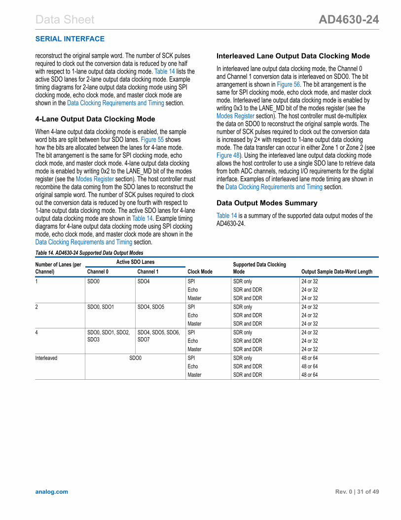
Data Output Modes SummaryTable 14 is a summary of the supported data output modes of theAD4630-24.
Table 14. AD4630-24 Supported Data Output Modes
Number of Lanes (perChannel)
Active SDO LanesClock Mode
Supported Data ClockingMode Output Sample Data-Word LengthChannel 0 Channel 1
1 SDO0 SDO4 SPI SDR only 24 or 32Echo SDR and DDR 24 or 32Master SDR and DDR 24 or 32
2 SDO0, SDO1 SDO4, SDO5 SPI SDR only 24 or 32Echo SDR and DDR 24 or 32Master SDR and DDR 24 or 32
4 SDO0, SDO1, SDO2,SDO3
SDO4, SDO5, SDO6,SDO7
SPI SDR only 24 or 32Echo SDR and DDR 24 or 32Master SDR and DDR 24 or 32
Interleaved SDO0 SPI SDR only 48 or 64Echo SDR and DDR 48 or 64Master SDR and DDR 48 or 64
Data Sheet AD4630-24SERIAL INTERFACE
analog.com Rev. 0 | 32 of 49
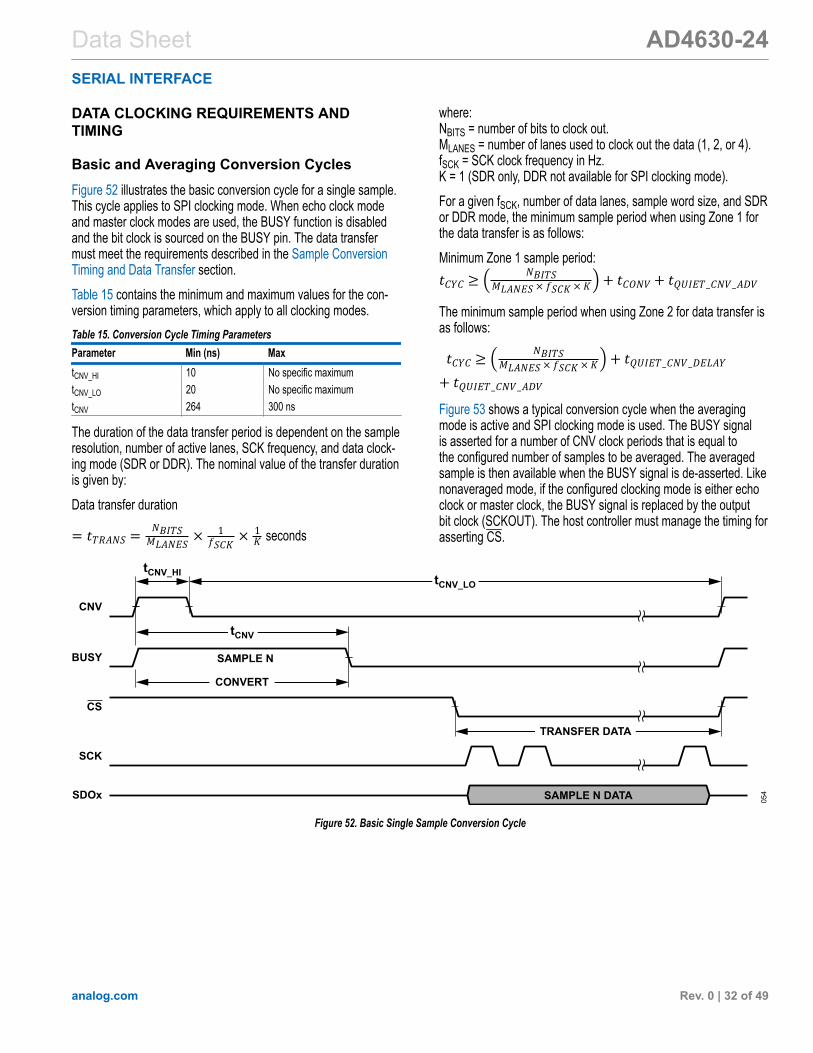
DATA CLOCKING REQUIREMENTS ANDTIMING
Basic and Averaging Conversion CyclesFigure 52 illustrates the basic conversion cycle for a single sample.This cycle applies to SPI clocking mode. When echo clock modeand master clock modes are used, the BUSY function is disabledand the bit clock is sourced on the BUSY pin. The data transfermust meet the requirements described in the Sample ConversionTiming and Data Transfer section.Table 15 contains the minimum and maximum values for the con-version timing parameters, which apply to all clocking modes.Table 15. Conversion Cycle Timing ParametersParameter Min (ns) MaxtCNV_HI 10 No specific maximumtCNV_LO 20 No specific maximumtCNV 264 300 ns
The duration of the data transfer period is dependent on the sampleresolution, number of active lanes, SCK frequency, and data clock-ing mode (SDR or DDR). The nominal value of the transfer durationis given by:Data transfer duration= tTRANS = NBITSMLANES × 1fSCK × 1K seconds
where:NBITS = number of bits to clock out.MLANES = number of lanes used to clock out the data (1, 2, or 4).fSCK = SCK clock frequency in Hz.K = 1 (SDR only, DDR not available for SPI clocking mode).For a given fSCK, number of data lanes, sample word size, and SDRor DDR mode, the minimum sample period when using Zone 1 forthe data transfer is as follows:Minimum Zone 1 sample period:tCYC ≥ NBITSMLANES × fSCK × K + tCONV+ tQUIET_CNV_ADVThe minimum sample period when using Zone 2 for data transfer isas follows: tCYC ≥ NBITSMLANES × fSCK × K + tQUIET_CNV_DELAY+ tQUIET_CNV_ADVFigure 53 shows a typical conversion cycle when the averagingmode is active and SPI clocking mode is used. The BUSY signalis asserted for a number of CNV clock periods that is equal tothe configured number of samples to be averaged. The averagedsample is then available when the BUSY signal is de-asserted. Likenonaveraged mode, if the configured clocking mode is either echoclock or master clock, the BUSY signal is replaced by the outputbit clock (SCKOUT). The host controller must manage the timing forasserting CS.
Figure 52. Basic Single Sample Conversion Cycle

Data Sheet AD4630-24SERIAL INTERFACE
analog.com Rev. 0 | 33 of 49
Figure 53. Example Conversion Cycle for Averaging Mode
SPI Clocking Mode Timing Diagrams
1-Lane, SDR ModeFigure 6 shows a conversion cycle for 1-lane data output using SDR mode (1 bit per clock cycle). This cycle timing is the same for both ADCchannels.
2-Lane, SDR ModeFigure 54 shows a conversion cycle for 2-lane data output using SDR clocking mode. Figure 54 shows the timing for Channel 0, but thisdiagram also applies to Channel 1. See the 2-Lane Output Data Clocking Mode section for a detailed explanation.
Figure 54. 2-Lane Mode, SDR Timing Diagram

Data Sheet AD4630-24SERIAL INTERFACE
analog.com Rev. 0 | 34 of 49
4-Lane, SDR ModeFigure 55 shows a conversion cycle for 4-lane data output using SDR clocking mode. Figure 55 shows the timing for Channel 0, but thisdiagram also applies for Channel 1. See the 4-Lane Output Data Clocking Mode section for a detailed explanation.
Figure 55. 4-Lane, SDR Timing Diagram
Interleaved Mode Timing, SDR ModeFigure 56 shows a conversion cycle for interleaved data output, SDR clocking mode. See the Interleaved-Lane Output Data Clocking Modesection for a detailed explanation.
Figure 56. Interleaved Mode, SDR Timing Diagram
Data Sheet AD4630-24SERIAL INTERFACE
analog.com Rev. 0 | 35 of 49
Echo Clock Timing Diagrams
1-Lane, SDR Mode, Echo Clock ModeFigure 7 shows the timing relationships for SDR mode (1 bit perSCK period) in 1-lane echo clock mode. The timing relationshipsbetween the signals apply to both 24-bit and 32-bit sample wordformats.SCKOUT is a delayed version of the incoming SCK. The delay(tDSDO) has a maximum value of 5.6 ns (at VIO > 1.71 V).Changes the in SDOx logic states are aligned to the rising edgesof SCKOUT. The clock and data edge alignments are the same for1-lane, 2-lane, and 4-lane output data modes.
1-Lane, DDR Mode, Echo Clock ModeFigure 8 shows the timing relationships for DDR mode (2-bit transi-tions per SCKOUT period) in 1-lane echo clock mode. The timingrelationships between the signals apply to both 24-bit and 32-bitsample word formats.Similar to SDR mode, SCKOUT is a delayed version of the incom-ing SCK. Changes in the SDOx logic states are aligned to both therising and falling edges of SCKOUT.
Master Clock Mode Timing
1-Lane, Master Clock Mode, SDRFigure 9 shows the timing relationships for master clock modewhen using SDR mode and 1-lane output data clocking mode.Similar to echo clock mode, the clock rising edges are alignedto the data bit transitions. The frequency of the SCKOUT signalis controlled by the OSC_DIV value programmed in the internaloscillator register (see the Internal Oscillator Register section).
1-Lane, Master Clock Mode, DDRFigure 10 shows the timing relationships for master clock modewhen using DDR mode. Similar to echo clock mode, the risingand falling clock edges are aligned to the data bit transitions. Thefrequency of the SCKOUT signal is controlled by the OSC_DIVvalue programmed in the internal oscillator register (see the InternalOscillator Register section).

Data Sheet AD4630-24LAYOUT GUIDELINES
analog.com Rev. 0 | 36 of 49
The following layout guidelines are recommended to achieve maxi-mum performance out of the AD4630-24: The AD4630-24 contains internal 1 μF bypass capacitors for
VDD_5V and VDD_1.8V, while VIO contains an internal 0.2 μFcapacitor. Therefore, no external bypass capacitors are required,saving board space and reducing BOM count and layout sensi-tivity.
It is recommended to have all the analog signals to flow infrom the left side of the AD4630-24 and all the digital signals toflow in-out from the right side of AD4630-24 because this helpsisolate analog signals from digital signals.
Use a solid ground plane under the AD4630-24 and connect allthe analog ground (GND) pins and digital ground (IOGND) pinsto the shared ground plane to avoid the formation of groundloops.
Traces routed to either the REFIN pin or REF pins must be iso-lated/shielded from other signals. Avoid routing signals beneaththe reference trace (REFIN or REF). The REF pins are connect-ed to an internal 2 µF capacitor, eliminating the need to placea decoupling capacitor on the output of the external referencebuffer. If a noise reduction filter is placed between the output ofthe reference (or buffer) and the chosen reference input, the filtermust be placed as close as possible to the AD4630-24.

Data Sheet AD4630-24REGISTERS
analog.com Rev. 0 | 37 of 49
The AD4630-24 has programmable user registers that are usedto configure the device. These registers can be accessed whilethe AD4630-24 is in register configuration mode. Table 16 detailsthe AD4630-24 user registers and the bit fields in the registers.The Register Details section details the functions of each of the bit
fields. The access mode specifies whether the register is comprisedonly of read-only bits (R) or a mix of read-only and read/writebits (R/W). Read-only bits cannot be overwritten by a SPI writetransaction, whereas read/write bits can be overwritten.
Table 16. AD4630-24 Register SummaryReg Name Bits Bit 7 Bit 6 Bit 5 Bit 4 Bit 3 Bit 2 Bit 1 Bit 0 Reset R/W0x00 INTERFACE_CONFIG
_A[7:0] SW_RESET RESERVED ADDR_ASC
ENSIONSDO_ENABLE
RESERVED SW_RESETX
0x10 R/W
0x01 INTERFACE_CONFIG_B
[7:0] SINGLE_INST STALLING RESERVED SHORT_INSTRUCTION
RESERVED 0x00 R/W
0x02 DEVICE_CONFIG [7:0] RESERVED OPERATING_MODES
0x00 R/W
0x03 CHIP_TYPE [7:0] RESERVED [7:4] CHIP_TYPE 0x07 R0x04 PRODUCT_ID_L [7:0] PRODUCT_ID[7:0] 0x00 R0x05 PRODUCT_ID_H [7:0] PRODUCT_ID[15:8] 0x20 R0x06 CHIP_GRADE [7:0] GRADE DEVICE_REVISION 0x01 R0x0A SCRATCH_PAD [7:0] SCRATCH_VALUE 0x00 R/W0x0B SPI_REVISION [7:0] SPI_TYPE VERSION 0x81 R0x0C VENDOR_L [7:0] VID[7:0] 0x56 R0x0D VENDOR_H [7:0] VID[15:8] 0x04 R0x0E STREAM_MODE [7:0] LOOP_COUNT 0x00 R/W0x10 INTERFACE_CONFIG
_C[7:0] RESERVED 0x00 R/W
0x11 INTERFACE_STATUS_A
[7:0] RESERVED CLOCK_COUNT_ER
R
RESERVED 0x00 R/W
0x14 EXIT_CFG_MD [7:0] RESERVED EXIT_CONFIG_MD
0x00 R/W
0x15 AVG [7:0] AVG_SYNC RESERVED AVG_VAL 0x00 R/W0x16 OFFSET_CH0_LB [7:0] CH0_USER_OFFSET[7:0] 0x00 R/W0x17 OFFSET_CH0_MB [7:0] CH0_USER_OFFSET[15:8] 0x00 R/W0x18 OFFSET_CH0_HB [7:0] CH0_USER_OFFSET[23:16] 0x00 R/W0x19 OFFSET_CH1_LB [7:0] CH1_USER_OFFSET[7:0] 0x00 R/W0x1A OFFSET_CH1_MB [7:0] CH1_USER_OFFSET[15:8] 0x00 R/W0x1B OFFSET_CH1_HB [7:0] CH1_USER_OFFSET[23:16] 0x00 R/W0x1C GAIN_CH0_LB [7:0] CH0_USER_GAIN[7:0] 0x00 R/W0x1D GAIN_CH0_HB [7:0] CH0_USER_GAIN[15:8] 0x80 R/W0x1E GAIN_CH1_LB [7:0] CH1_USER_GAIN[7:0] 0x00 R/W0x1F GAIN_CH1_HB [7:0] CH1_USER_GAIN[15:8] 0x80 R/W0x20 MODES [7:0] LANE_MD CLK_MD DDR_MD OUT_DATA_MD 0x00 R/W0x21 OSCILLATOR [7:0] OSC_LIMIT OSC_DIV 0x00 R/W0x22 IO [7:0] RESERVED IO2X 0x00 R/W0x23 TEST_PAT_BYTE0 [7:0] TEST_DATA_PAT[7:0] 0x0F R/W0x24 TEST_PAT_BYTE1 [7:0] TEST_DATA_PAT[15:8] 0x0F R/W0x25 TEST_PAT_BYTE2 [7:0] TEST_DATA_PAT[23:16] 0x5A R/W0x26 TEST_PAT_BYTE3 [7:0] TEST_DATA_PAT[31:24] 0x5A R/W0x34 DIG_DIAG [7:0] POWERUP
COMPLETEDRESET_OC
CURREDRESERVED FUSE_CR
C_EN0x40 R/W
0x35 DIG_ERR [7:0] RESERVED FUSE_CRC_ERR
0x00 R/W

Data Sheet AD4630-24REGISTER DETAILS
analog.com Rev. 0 | 38 of 49
INTERFACE CONFIGURATION A REGISTERAddress: 0x00, Reset: 0x10, Name: INTERFACE_CONFIG_AInterface configuration settings.
Table 17. Bit Descriptions for INTERFACE_CONFIG_ABits Bit Name Description Reset Access7 SW_RESET First of Two SW_RESET Bits. This bit appears in two locations in this register. Both locations must be written
at the same time to trigger a software reset of the part. All registers except for this register are reset to theirdefault values.
0x0 R/W
6 RESERVED Reserved. 0x0 R5 ADDR_ASCENSION Determines sequential addressing behavior. 0x0 R
0: address accessed is decremented by one for each data byte when streaming.1: not a valid option.
4 SDO_ENABLE SDO Pin Enable. 0x1 R[3:1] RESERVED Reserved. 0x0 R0 SW_RESETX Second of Two SW_RESET Bits. This bit appears in two locations in this register. Both locations must be
written at the same time to trigger a software reset of the part. All registers except for this register are resetto their default values.
0x0 R/W
INTERFACE CONFIGURATION B REGISTERAddress: 0x01, Reset: 0x00, Name: INTERFACE_CONFIG_BAdditional interface configuration settings.
Table 18. Bit Descriptions for INTERFACE_CONFIG_BBits Bit Name Description Reset Access7 SINGLE_INST Select streaming or single instruction mode. 0x0 R/W
0: streaming mode is enabled. The address decrements as successive data bytes are received.1: single instruction mode is enabled.
6 STALLING Reserved for Stalling Feature. 0x0 R/W[5:4] RESERVED Reserved. 0x0 R3 SHORT_INSTRUCTION Set the instruction phase address to 7 bits or 15 bits. 0x0 R
0: 15-bit addressing.1: 7-bit addressing.
[2:0] RESERVED Reserved. 0x0 R

Data Sheet AD4630-24REGISTER DETAILS
analog.com Rev. 0 | 39 of 49
DEVICE CONFIGURATION REGISTERAddress: 0x02, Reset: 0x00, Name: DEVICE_CONFIG
Table 19. Bit Descriptions for DEVICE_CONFIGBits Bit Name Description Reset Access[7:2] RESERVED Reserved. 0x0 R[1:0] OPERATING_MODES Power Modes. 0x0 R/W
00: normal operating mode.11: shutdown mode.
CHIP TYPE REGISTERAddress: 0x03, Reset: 0x07, Name: CHIP_TYPEThe chip type is used to identify the family of Analog Devices products a given device belongs to. Use the chip type with the product ID touniquely identify a given product.
Table 20. Bit Descriptions for CHIP_TYPEBits Bit Name Description Reset Access[7:4] RESERVED Reserved. 0x0 R[3:0] CHIP_TYPE Precision ADC. 0x7 R
PRODUCT ID LOW REGISTERAddress: 0x04, Reset: 0x00, Name: PRODUCT_ID_LLow byte of the product ID.
Table 21. Bit Descriptions for PRODUCT_ID_LBits Bit Name Description Reset Access[7:0] PRODUCT_ID, Bits[7:0] This is the device chip type/family. Use the product ID with the chip type to identify a product. 0x0 R
PRODUCT ID HIGH REGISTERAddress: 0x05, Reset: 0x20, Name: PRODUCT_ID_HHigh byte of the product ID.

Data Sheet AD4630-24REGISTER DETAILS
analog.com Rev. 0 | 40 of 49
Table 22. Bit Descriptions for PRODUCT_ID_HBits Bit Name Description Reset Access[7:0] PRODUCT_ID, Bits[15:8] This is the device chip type/family. Use the product ID with the chip type to identify a product. 0x20 R
CHIP GRADE REGISTERAddress: 0x06, Reset: 0x01, Name: CHIP_GRADEIdentifies product variations and device revisions.
Table 23. Bit Descriptions for CHIP_GRADEBits Bit Name Description Reset Access[7:3] GRADE This is the device performance grade. 0x0 R[2:0] DEVICE_REVISION This is the device hardware revision. 0x1 R
SCRATCHPAD REGISTERAddress: 0x0A, Reset: 0x00, Name: SCRATCH_PADThis register can be used to test writes and reads.
Table 24. Bit Descriptions for SCRATCH_PADBits Bit Name Description Reset Access[7:0] SCRATCH_VALUE Software Scratchpad. Software can write to and read from this location without any device side effects. 0x0 R/W
SPI REVISION REGISTERAddress: 0x0B, Reset: 0x81, Name: SPI_REVISIONIndicates the SPI revision.
Table 25. Bit Descriptions for SPI_REVISIONBits Bit Name Description Reset Access[7:6] SPI_TYPE Always reads as 0x2. 0x2 R[5:0] VERSION SPI Version. 0x1 R
01: draft
Data Sheet AD4630-24REGISTER DETAILS
analog.com Rev. 0 | 41 of 49
VENDOR ID LOW REGISTERAddress: 0x0C, Reset: 0x56, Name: VENDOR_LLow byte of the vendor ID.
Table 26. Bit Descriptions for VENDOR_LBits Bit Name Description Reset Access[7:0] VID[7:0] Analog Devices Vendor ID. 0x56 R
VENDOR ID HIGH REGISTERAddress: 0x0D, Reset: 0x04, Name: VENDOR_HHigh byte of the vendor ID.
Table 27. Bit Descriptions for VENDOR_HBits Bit Name Description Reset Access[7:0] VID[15:8] Analog Devices Vendor ID. 0x4 R
STREAM MODE REGISTERAddress: 0x0E, Reset: 0x00, Name: STREAM_MODEDefines the length of the loop when streaming data.
Table 28. Bit Descriptions for STREAM_MODEBits Bit Name Description Reset Access[7:0] LOOP_COUNT Sets the data byte count before looping to start address. When streaming data, a nonzero value sets the number
of data bytes written before the address loops back to the start address. A maximum of 255 bytes can be writtenusing this approach. A value of 0x00 disables the loop back so that addressing wraps around at the upper andlower limits of the memory. After writing this register, the loop value applies only to the following SPI instruction andauto clears upon the end of that instruction.
0x0 R/W

Data Sheet AD4630-24REGISTER DETAILS
analog.com Rev. 0 | 42 of 49
INTERFACE CONFIGURATION C REGISTERAddress: 0x10, Reset: 0x00, Name: INTERFACE_CONFIG_CAdditional interface configuration settings.
Table 29. Bit Descriptions for INTERFACE_CONFIG_CBits Bit Name Description Reset Access[7:0] RESERVED Reserved. 0x0 R
INTERFACE STATUS A REGISTERAddress: 0x11, Reset: 0x00, Name: INTERFACE_STATUS_AStatus bits are set to 1 to indicate an active condition. The status bits can be cleared by writing a 1 to the corresponding bit location.
Table 30. Bit Descriptions for INTERFACE_STATUS_ABits Bit Name Description Reset Access[7:5] RESERVED Reserved. 0x0 R4 CLOCK_COUNT_ERR Incorrect Number of Clocks Detected in a Transaction. 0x0 R/W[3:0] RESERVED Reserved. 0x0 R
EXIT CONFIGURATION MODE REGISTERAddress: 0x14, Reset: 0x00, Name: EXIT_CFG_MD
Table 31. Bit Descriptions for EXIT_CFG_MDBits Bit Name Description Reset Access[7:1] RESERVED Reserved. 0x0 R0 EXIT_CONFIG_MD Exit Register Config Mode. Write 1 to exit register configuration mode. Self clearing upon CS = 1. 0x0 R/W

Data Sheet AD4630-24REGISTER DETAILS
analog.com Rev. 0 | 43 of 49
AVERAGING MODE REGISTERAddress: 0x15, Reset: 0x00, Name: AVG
Table 32. Bit Descriptions for AVGBits Bit Name Description Reset Access7 AVG_SYNC Averaging Filter Reset. 1 = reset, self clearing. 0x0 R/W[6:5] RESERVED Reserved. 0x0 R[4:0] AVG_VAL Averaging Filter Block Length, 2N. 0x0 R/W
0x00 = no averaging.0x01 = 21 samples.0x02 = 22 samples.0x03 = 23 samples.0x04 = 24 samples.0x05 = 25 samples.…0x0F = 215 samples.0x10 = 216 samples.0x11 through 0x1F = invalid.
CHANNEL 0 OFFSET REGISTERSAddress: 0x16, Reset: 0x00, Name: OFFSET_CH0_LB
Table 33. Bit Descriptions for OFFSET_CH0_LBBits Bit Name Description Reset Access[7:0] CH0_USER_OFFSET[7:0] 24-Bit Channel 0 Offset. Twos complement (signed). 1 LSB = (VREF/223)/Gain. See the Channel 0
Gain Registers section for a description of the gain parameter.0x0 R/W
Address: 0x17, Reset: 0x00, Name: OFFSET_CH0_MB
Table 34. Bit Descriptions for OFFSET_CH0_MBBits Bit Name Description Reset Access[7:0] CH0_USER_OFFSET[15:8] 24-Bit Channel 0 Offset. Twos complement (signed). 1 LSB = (VREF/223)/Gain. See the Channel 0
Gain Registers section for a description of the gain parameter.0x0 R/W

Data Sheet AD4630-24REGISTER DETAILS
analog.com Rev. 0 | 44 of 49
Address: 0x18, Reset: 0x00, Name: OFFSET_CH0_HB
Table 35. Bit Descriptions for OFFSET_CH0_HBBits Bit Name Description Reset Access[7:0] CH0_USER_OFFSET[23:16] 24-Bit Channel 0 Offset. Twos complement (signed). 1 LSB = (VREF/223)/Gain. See the Channel 0
Gain Registers section for a description of the gain parameter.0x0 R/W
CHANNEL 1 OFFSET REGISTERSAddress: 0x19, Reset: 0x00, Name: OFFSET_CH1_LB
Table 36. Bit Descriptions for OFFSET_CH1_LBBits Bit Name Description Reset Access[7:0] CH1_USER_OFFSET[7:0] 24-Bit Channel 1 Offset. Twos complement (signed). 1 LSB = (VREF/223)/Gain. See the Channel 1
Gain Registers section for a description of the gain parameter value.0x0 R/W
Address: 0x1A, Reset: 0x00, Name: OFFSET_CH1_MB
Table 37. Bit Descriptions for OFFSET_CH1_MBBits Bit Name Description Reset Access[7:0] CH1_USER_OFFSET[15:8] 24-Bit Channel 1 Offset. Twos complement (signed). 1 LSB = (VREF/223)/Gain. See the Channel 1
Gain Registers section for a description of the gain parameter value.0x0 R/W
Address: 0x1B, Reset: 0x00, Name: OFFSET_CH1_HB
Table 38. Bit Descriptions for OFFSET_CH1_HBBits Bit Name Description Reset Access[7:0] CH1_USER_OFFSET[23:16] 24-Bit Channel 1 Offset. Twos complement (signed). 1 LSB = (VREF/223)/Gain. See the Channel 1
Gain Registers section for a description of the gain parameter value.0x0 R/W

Data Sheet AD4630-24REGISTER DETAILS
analog.com Rev. 0 | 45 of 49
CHANNEL 0 GAIN REGISTERSAddress: 0x1C, Reset: 0x00, Name: GAIN_CH0_LB
Table 39. Bit Descriptions for GAIN_CH0_LBBits Bit Name Description Reset Access[7:0] CH0_USER_GAIN[7:0] Channel 0 Gain Word (Unsigned). Multiplier output = input × Gain Word/0x8000. Maximum effective gain
= 0xFFFF/0x8000 = 1.99997.0x00 R/W
Address: 0x1D, Reset: 0x80, Name: GAIN_CH0_HB
Table 40. Bit Descriptions for GAIN_CH0_HBBits Bit Name Description Reset Access[7:0] CH0_USER_GAIN[15:8] Channel 0 Gain Word (Unsigned). Multiplier output = input × Gain Word/0x8000. Maximum effective
gain = 0xFFFF/0x8000 = 1.99997.0x80 R/W
CHANNEL 1 GAIN REGISTERSAddress: 0x1E, Reset: 0x00, Name: GAIN_CH1_LB
Table 41. Bit Descriptions for GAIN_CH1_LBBits Bit Name Description Reset Access[7:0] CH1_USER_GAIN[7:0] Channel 1 Gain Word (Unsigned). Multiplier output = input × Gain Word/0x8000. Maximum effective gain
= 0xFFFF/0x8000 = 1.99997.0x00 R/W
Address: 0x1F, Reset: 0x80, Name: GAIN_CH1_HB
Table 42. Bit Descriptions for GAIN_CH1_HBBits Bit Name Description Reset Access[7:0] CH1_USER_GAIN[15:8] Channel 1 Gain Word (Unsigned). Multiplier output = input × Gain Word/0x8000. Maximum effective
gain = 0xFFFF/0x8000 = 1.99997.0x80 R/W
Data Sheet AD4630-24REGISTER DETAILS
analog.com Rev. 0 | 46 of 49
MODES REGISTERAddress: 0x20, Reset: 0x00, Name: MODES
Table 43. Bit Descriptions for MODESBits Bit Name Description Reset Access[7:6] LANE_MD Lane Mode Select. 0x0 R/W
00 = one lane per channel.01 = two lanes per channel.10 = four lanes per channel.11 = Channel 0 and Channel 1 interleaved on SDO0.
[5:4] CLK_MD Clock Mode Select. 0x0 R/W00 = SPI clocking mode.01 = echo clock mode.10 = master clock mode.11 = invalid setting.
3 DDR_MD DDR Mode Enable/Disable. 0x0 R/W0 = SDR.1 = DDR (only valid for echo clock and master clock modes).
[2:0] OUT_DATA_MD Output Data Mode Select. 0x0 R/W000 = 24-bit differential data.001 = 16-bit differential data + 8-bit common mode data.010 = 24-bit differential data + 8-bit common mode data.011 = 30-bit averaged differential data + OR-bit + SYNC-bit.100 = 32-bit test data pattern (see the Test Pattern Registers section).
INTERNAL OSCILLATOR REGISTERAddress: 0x21, Reset: 0x00, Name: OSCILLATOR
Table 44. Bit Descriptions for OSCILLATORBits Bit Name Description Reset Access[7:2] OSC_LIMIT Oscillator Limit Setting. Oscillator is limited to this number of clock pulses plus one. Automatically calculated by the
AD4630-24 based on the data word size, number of active SDO lanes, and data rate mode (SDR or DDR).0x0 R
[1:0] OSC_DIV Oscillator Frequency Divider Setting. 0x0 R/W00 = no divide (divide by 1).01 = divide by 2.10 = divide by 4.11 = invalid setting.

Data Sheet AD4630-24REGISTER DETAILS
analog.com Rev. 0 | 47 of 49
OUTPUT DRIVER REGISTERAddress: 0x22, Reset: 0x00, Name: IO
Table 45. Bit Descriptions for IOBits Bit Name Description Reset Access[7:1] RESERVED Reserved. 0x0 R0 IO2X Double Output Driver Strength. 0x0 R/W
1 = double output driver strength.0 = normal output driver strength.
TEST PATTERN REGISTERSAddress: 0x23, Reset: 0x0F, Name: TEST_PAT_BYTE0
Table 46. Bit Descriptions for TEST_PAT_BYTE0Bits Bit Name Description Reset Access[7:0] TEST_DATA_PAT[7:0] 32-Bit Test Pattern. Applied to both channels when OUT_DATA_MD = 4 (see the Modes Register section). 0xF R/W
Address: 0x24, Reset: 0x0F, Name: TEST_PAT_BYTE1
Table 47. Bit Descriptions for TEST_PAT_BYTE1Bits Bit Name Description Reset Access[7:0] TEST_DATA_PAT[15:8] 32-Bit Test Pattern. Applied to both channels when OUT_DATA_MD = 4 (see the Modes Register
section).0xF R/W
Address: 0x25, Reset: 0x5A, Name: TEST_PAT_BYTE2
Table 48. Bit Descriptions for TEST_PATBYTE2Bits Bit Name Description Reset Access[7:0] TEST_DATA_PAT[23:16] 32-Bit Test Pattern. Applied to both channels when OUT_DATA_MD = 4 (see the Modes Register
section).0x5A R/W
Data Sheet AD4630-24REGISTER DETAILS
analog.com Rev. 0 | 48 of 49
Address: 0x26, Reset: 0x5A, Name: TEST_PAT_BYTE3
Table 49. Bit Descriptions for TEST_PAT_BYTE3Bits Bit Name Description Reset Access[7:0] TEST_DATA_PAT[31:24] 32-Bit Test Pattern. Applied to both channels when OUT_DATA_MD = 4 (see the Modes Register
section).0x5A R/W
DIGITAL DIAGNOSTICS REGISTERAddress: 0x34, Reset: 0x40, Name: DIG_DIAG
Table 50. Bit Descriptions for DIG_DIAGBits Bit Name Description Reset Access7 POWERUP_COMPLETED 1 = Power-Up Completed. 0x0 R6 RESET_OCCURRED Reset Occurred. This bit is set to 1 upon a reset event. Write 1 to clear (useful for detecting
brownouts).0x1 R/W1C
[5:1] RESERVED Reserved. 0x0 R0 FUSE_CRC_EN Fuse CRC Enable. Write a 1 to force recheck of CRC. 0x0 R/W
DIGITAL ERRORS REGISTERAddress: 0x35, Reset: 0x00, Name: DIG_ERR
Table 51. Bit Descriptions for DIG_ERRBits Bit Name Description Reset Access[7:1] RESERVED Reserved. 0x0 R0 FUSE_CRC_ERR Fuse CRC Error. This bit is set to 1 upon a fuse CRC error. Write 1 to clear. 0x0 R/W1C

Data Sheet AD4630-24OUTLINE DIMENSIONS
©2021 Analog Devices, Inc. All rights reserved. Trademarks andregistered trademarks are the property of their respective owners.One Analog Way, Wilmington, MA 01887-2356, U.S.A.
Rev. 0 | 49 of 49
Figure 57. 64-Ball Chip Scale Package Ball Grid Array [CSP_BGA](BC-64-8)
Dimensions shown in millimeters
Updated: November 26, 2021
ORDERING GUIDEModel1 Temperature Range Package Description Package OptionAD4630-24BBCZ −40°C to +125°C CHIP SCALE BGA BC-64-8AD4630-24BBCZ-RL −40°C to +125°C CHIP SCALE BGA BC-64-81 Z = RoHS Compliant Part.
EVALUATION BOARDSModel1 DescriptionEVAL-AD4630-24-KTZ Evaluation KitEVAL-AD4630-24FMCZ Evaluation Board1 Z = RoHS Compliant Part.