Embed Size (px)
Citation preview

Broadband Analog Time Delay to 24 GHzData Sheet HMC911
Rev. B Document Feedback Information furnished by Analog Devices is believed to be accurate and reliable. However, no responsibility is assumed by Analog Devices for its use, nor for any infringements of patents or other rights of third parties that may result from its use. Specifications subject to change without notice. No license is granted by implication or otherwise under any patent or patent rights of Analog Devices. Trademarks and registered trademarks are the property of their respective owners.
One Technology Way, P.O. Box 9106, Norwood, MA 02062-9106, U.S.A.Tel: 781.329.4700 ©2014–2016 Analog Devices, Inc. All rights reserved. Technical Support www.analog.com
FEATURES Very wide bandwidth to 24 GHz Time delay range: 70 ps typical Single-ended or differential operation Adjustable differential output amplitude with 780 mV p-p typical
at 10 GHz Delay control modulation bandwidth: 1.6 GHz typical Single supply: 3.3 V 24-terminal ceramic, leadless chip carrier (LCC)
APPLICATIONS Synchronization of clock and data Transponder design Serial data transmissions up to 32 Gbps Broadband test and measurement RF ATE applications
FUNCTIONAL BLOCK DIAGRAM
TEMPERATURECOMPENSATION
AND BIAS
136EN VEE
5GND 14 GND
4INN 15 QN
3INP 16 QP
2GND 17 GND
1NC 18 NC
7V
EE
8V
EE
9V
DC
P
10V
DC
N
11V
EE
12V
AC
19V
CC
20V
CC
21V
CC
22V
CC
23V
CC
24V
CC
VCC
VCC
VCC
VCC
AMP BUF
GND
PACKAGEBASE
BUF
HMC911
14
816
-00
1
Figure 1.
GENERAL DESCRIPTION The HMC911 is a broadband time delay with 62 ps to 75 ps continuously adjustable delay range to 24 GHz. The delay control is linearly monotonic with respect to the differential delay control voltage (VDCP and VDCN), and the control input has a modulation bandwidth of 1.6 Hz. The HMC911 provides a differential output voltage with constant amplitude for single-ended or differential input voltages above the input sensitivity level, and the output voltage swing can be adjusted using the VAC control pin.
The HMC911 features internal temperature compensation and bias circuitry to minimize delay variations with temperature. All RF inputs and outputs of the HMC911 are internally terminated with 50 Ω to VCC and can be ac-coupled or dc-coupled. Output pins connect directly to a 50 Ω to VCC terminated system. However, use dc blocking capacitors if the terminated system input is 50 Ω to a dc voltage other than VCC.
The HMC911 is available in a RoHS-compliant, 24-terminal, ceramic, leadless chip carrier.

HMC911 Data Sheet
Rev. B | Page 2 of 13
TABLE OF CONTENTS Features .............................................................................................. 1 Applications ....................................................................................... 1 Functional Block Diagram .............................................................. 1 General Description ......................................................................... 1 Revision History ............................................................................... 2 Specifications ..................................................................................... 3 Absolute Maximum Ratings ............................................................ 4
ESD Caution .................................................................................. 4
Pin Configuration and Function Descriptions ..............................5 Interface Schematics .....................................................................6
Typical Performance Characteristics ..............................................7 Applications Information .............................................................. 11
Evaluation Printed Circuit Board (PCB)................................. 11 Typical Application Circuit ........................................................... 12 Outline Dimensions ....................................................................... 13
Ordering Guide .......................................................................... 13
REVISION HISTORY 10/2016—Rev. v02.0614 to Rev. B Updated Format .................................................................. Universal Changes to Product Title, Features Section, and General Description Section .......................................................................... 1 Changes to Table 1 ............................................................................ 3 Changes to Table 2 ............................................................................ 4 Changes to Table 3 ............................................................................ 5 Changes to Figure 4 and Figure 6 ................................................... 6
Changes to Figure 13 Caption ......................................................... 7 Changes to Figure 17 Caption and Figure 20 Caption ................. 8 Changes to Figure 31 Caption ...................................................... 10 Changes to Table 4 .......................................................................... 11 Changes to Typical Application Circuit Section ........................ 12 Updated Outline Dimensions ....................................................... 13 Changes to Ordering Guide .......................................................... 13

Data Sheet HMC911
Rev. B | Page 3 of 13
SPECIFICATIONS TA = 25°C, VCC = 3.3 V, VAC = 2.6 V, VEE = GND = 0 V, unless otherwise noted.
Table 1. Parameter Min Typ Max Unit Test Conditions/Comments POWER SUPPLY
Voltage 3.13 3.3 3.47 V ±5% tolerance Current 460 530 mA
TIME DELAY RANGE VDCP = 3.9 V, VDCN = 3.3 V 10 GHz 62 70 71 ps 18 GHz 64 70 73 ps 22 GHz 66 70 75 ps
TIME DELAY SENSITIVITY Voltage 116 ps/V Temperature 0.04 ps/°C VDCP = VDCN = 3.3 V at 18 GHz
PHASE SHIFT RANGE VDCP = 3.9 V, VDCN = 3.3 V 10 GHz 210 250 Degrees 18 GHz 400 475 Degrees 22 GHz 515 595 Degrees
MAXIMUM DATA RATE 32 Gbps MAXIMUM CLOCK FREQUENCY 24 GHz DELAY CONTROL
Modulation Bandwidth 1.6 GHz Voltage (VDCP and VDCN) VCC − 0.6 VCC + 0.6 V
INPUT VOLTAGE Low (VIL) VCC − 500 VCC − 200 VCC − 25 mV High (VIH) VCC + 25 VCC + 200 VCC + 500 mV
INPUT AMPLITUDE, PEAK TO PEAK Single Ended 50 1000 mV p-p Differential 100 2000 mV p-p
OUTPUT AMPLITUDE VAC = 2.6 V 10 GHz 370 390 640 mV p-p Single-ended 740 780 1280 mV p-p Differential 18 GHz 350 375 640 mV p-p Single-ended 700 750 1280 mV p-p Differential 22 GHz 340 350 640 mV p-p Single-ended
680 700 1280 mV p-p Differential CONTROL VOLTAGE (VAC) 1.7 2.6 2.7 V HARMONIC SUPPRESSION (fIN − 2fIN)1, 2 VDCP = VDCN = 3.3 V
10 GHz 21 32 dBc 20 GHz 19 30 dBc
RETURN LOSS Frequency < 24 GHz Input 9 dB Output 10 dB
RMS JITTER 0.3 ps, p-p 32 Gbps, 10101 … data TIME3
Rise (tR) 15 ps Fall (tF) 14 ps
PROPAGATION DELAY 480 ps VDCP = 2.7 V, VDCN = 3.3 V (relative to zero time delay) 1 Harmonic suppression measurements were taken for single-ended inputs and outputs. 2 fIN is the fundamental frequency. 3 VINPUT = differential 400 mV p-p, and fDATA = 22.5 Gbps, and pseudorandom bit sequences (PRBS) 233 − 1

HMC911 Data Sheet
Rev. B | Page 4 of 13
ABSOLUTE MAXIMUM RATINGS Table 2. Parameter Rating Power Supply Voltage (VCC) −0.5 V to +3.75 V Input Voltage (VIN) VCC – 1.2 V to
VCC + 0.6 V Output Voltage (VOUT) VCC – 1.2 V to
VCC + 0.6 V Delay Control Voltage (VDCP, VDCN) 0 V to VCC + 0.6 V Power-Down (Enable) Pin (EN) 0 V to VCC + 0.6 V
Amplitude Control (VAC) 0 V to VCC + 0.6 V Continuous Power Dissipation, PDISS (TA =
85°C, Derate 54.96 mW/°C above 85°C) 2.2 W
Thermal Resistance (Junction to Ground Paddle)
18.2°C/W
Channel Temperature (TC) 125°C Maximum Peak Reflow Temperature (MSL3)1 260°C Storage Temperature Range −65°C to +125°C Operating Temperature Range −40°C to +85°C Electrostatic Discharge (ESD)
Human Body Model (HBM) Class 1B
Stresses at or above those listed under Absolute Maximum Ratings may cause permanent damage to the product. This is a stress rating only; functional operation of the product at these or any other conditions above those indicated in the operational section of this specification is not implied. Operation beyond the maximum operating conditions for extended periods may affect product reliability.
ESD CAUTION
1 See the Ordering Guide section.

Data Sheet HMC911
Rev. B | Page 5 of 13
PIN CONFIGURATION AND FUNCTION DESCRIPTIONS
136EN VEE
5GND 14 GND
4INN 15 QN
3INP 16 QP
2GND 17 GND
1NC 18 NC
7V
EE
8V
EE
9V
DC
P
10V
DC
N
11V
EE
12V
AC
19V
CC
20V
CC
21V
CC
22V
CC
23V
CC
24V
CC
GND
PACKAGEBASE
HMC911TOP VIEW
(Not to Scale)
NOTES1. NC = NO CONNECT.2. EXPOSED PAD. CONNECT THE EXPOSED
PAD TO RF/DC GROUND 148
16-0
02
Figure 2. Pin Configuration
Table 3. Pin Function Descriptions Pin No. Mnemonic Description 1, 18 NC No Connect. These pins are not connected internally; however, all data shown herein was measured with these
pins connected to RF/dc ground externally. 2, 5, 14, 17 GND Ground Pin. Connect these signal grounds to 0 V. See Figure 3 for the interface schematic. 3 INP Positive Differential RF Input Pin. See Figure 4 for the interface schematic. 4 INN Negative Differential RF Input Pin. See Figure 4 for the interface schematic. 6 EN Enable Pin for the Time Delay. For normal operation, leave this pin open or apply 3.3 V. To disable the HMC911,
apply 0 V. When disabled, the total current consumption drops to 15 mA. See Figure 5 for the interface schematic. 7, 8, 11, 13 VEE Supply Grounds. Connect these pins to 0 V. See Figure 6 for the interface schematic. 9 VDCP Positive Differential Time Delay Control Pin. See Figure 7 for the interface schematic. 10 VDCN Negative Differential Time Delay Control Pin. See Figure 7 for the interface schematic. 12 VAC Output Amplitude Control Pin. See Figure 8 for the interface schematic. 15 QN Negative Differential RF Output Pin. See Figure 9 for the interface schematic. 16 QP Positive Differential RF Output Pin. See Figure 9 for the interface schematic. 19 to 24 VCC Positive Supply Pins. See Figure 10 for the interface schematic. EPAD Exposed Pad. Connect the exposed pad to RF/dc ground.
HMC911 Data Sheet
Rev. B | Page 6 of 13
INTERFACE SCHEMATICS
GND
1481
6-00
3
Figure 3. GND Interface Schematic
INP,INN
VEE
VCC
50Ω
148
16-0
04
Figure 4. INP and INN Interface Schematic
250Ω
20kΩ
EN
VEE
VCC
14
816-
00
5
Figure 5. EN Interface Schematic
GND
VEE
148
16-
00
6
Figure 6. VEE Interface Schematic
VDCP,VDCN
VEE
VCC
50Ω
1481
6-00
7
Figure 7. VDCP and VDCN Interface Schematic
VAC
VCC
VEE
148
16
-00
8
Figure 8. VAC Interface Schematic
VCC
VEE
QP,QN
50Ω
148
16-0
09
Figure 9. QN and QP Interface Schematic
GND
VCC
14
816
-01
0
Figure 10. VCC Interface Schematic

Data Sheet HMC911
Rev. B | Page 7 of 13
TYPICAL PERFORMANCE CHARACTERISTICS
–0.6 –0.4 –0.2 0 0.2 0.4 0.6
NO
RM
AL
IZE
D T
IME
DE
LA
Y (
ps)
DIFFERENTIAL DELAY CONTROL VOLTAGE (V)
0
10
20
30
40
50
60
70
80
10GHz16GHz20GHz22GHz24GHz
VAC = 2.6VVDCN = 3.3VVCC = 3.3V
14
816
-011
Figure 11. Normalized Time Delay vs. Differential Delay Control Voltage, Differential Delay Control Voltage Represents VDCP − VDCN Voltage on the X-Axis
–0.6 –0.4 –0.2 0 0.2 0.4 0.6
NO
RM
AL
IZE
D T
IME
DE
LA
Y (
ps)
DIFFERENTIAL DELAY CONTROL VOLTAGE (V)
0
10
20
30
40
50
60
70
80
+85°C+25°C–40°C
VAC = 2.6VVDCN = 3.3VVCC = 3.3V
14
816
-01
2
Figure 12. Normalized Time Delay vs. Differential Delay Control Voltage at 22 GHz for Various Temperatures, Differential Delay Control Voltage
Represents VDCP − VDCN Voltage on the X-Axis
5 6 7 8 9 10 11 1312 1514 16 1817 19 20
f IN P
OW
ER
– 2f IN
PO
WE
R (
dB
c)
FREQUENCY (GHz)
0
5
10
15
20
25
30
35
40
45
VDCP – VDCN = –0.6VVDCP – VDCN = –0.4VVDCP – VDCN = –0.2VVDCP – VDCN = 0VVDCP – VDCN = +0.2VVDCP – VDCN = +0.4VVDCP – VDCN = +0.6V
VAC = 2.6VVDCN = 3.3VVCC = 3.3V
14
816
-01
3
Figure 13. fIN Power – 2fIN Power vs. Frequency
–0.6 –0.4 –0.2 0 0.2 0.4 0.6
NO
RM
AL
IZE
D T
IME
DE
LA
Y (
ps)
DIFFERENTIAL DELAY CONTROL VOLTAGE (V)
0
10
20
30
40
50
60
70
80
3.13V3.30V3.47V
VAC = 2.6VVDCN = 3.3VVCC = 3.3V
148
16-
01
4
Figure 14. Normalized Time Delay vs. Differential Delay Control Voltage at 22 GHz for Various Voltages, Differential Delay Control Voltage Represents
VDCP − VDCN Voltage on the X-Axis
2 4 6 8 10 12 14 16 18 20 22 24
TIM
E D
EL
AY
(p
s)
FREQUENCY (GHz)
0
10
20
30
40
50
60
70
80VAC = 2.6VVDCN = 3.3VVCC = 3.3V
148
16-
01
5
Figure 15. Time Delay vs. Frequency at VDCP = 2.7 V to 3.9 V with 0.1 V Step
2 4 6 8 10 12 14 16 18 20 22
TIM
E D
EL
AY
ER
RO
R (
ps)
FREQUENCY (GHz)
–8
–6
–4
–2
0
2
4
6
8VDCP – VDCN = –0.6V (REFERENCE)VDCP – VDCN = –0.4VVDCP – VDCN = –0.2VVDCP – VDCN = 0VVDCP – VDCN = +0.2VVDCP – VDCN = +0.4VVDCP – VDCN = +0.6V
VAC = 2.6VVDCN = 3.3VVCC = 3.3V
148
16-
01
6
Figure 16. Time Delay Error vs. Frequency at Mean Frequency (fMEAN) = 18 GHz

HMC911 Data Sheet
Rev. B | Page 8 of 13
2 4 6 8 10 12 14 16 18 20 22 24
TIM
E D
EL
AY
(p
s)
FREQUENCY (GHz)
50
55
60
65
70
75
80
+85°C+25°C–40°C
VAC = 2.6VVDCN = 3.3VVCC = 3.3VVDCP = 3.9V
148
16-
01
7
Figure 17. Programmable Maximum Time Delay vs. Frequency for Various Temperatures
OU
TP
UT
VO
LT
AG
E S
WIN
G (
mV
p-p
)
SUPPLY VOLTAGE (V)
+85°C+25°C–40°C
200
225
250
275
300
325
350
375
400
3.13 3.30 3.47
VAC = 2.6VVDCP = VDCN = 3.3VfIN = 18GHz
148
16-
01
8
Figure 18. Single-Ended Output Voltage Swing vs. Supply Voltage for Various Temperatures
OU
TP
UT
VO
LT
AG
E S
WIN
G (
mV
p-p
)
AMPLITUDE CONTROL VOLTAGE (V)
+85°C+25°C–40°C
1.7 1.8 1.9 2.0 2.2 2.4 2.62.52.32.1 2.70
50
100
150
200
250
300
350
400
450VDCP = VDCN = 3.3VVCC = 3.3VfIN = 10GHz
148
16-
01
9
Figure 19. Single-Ended Output Voltage Swing vs. Amplitude Control Voltage (VAC) for Various Temperatures
2 4 6 8 10 12 14 16 18 20 22 24
TIM
E D
EL
AY
(p
s)
FREQUENCY (GHz)
50
55
60
65
70
75
80
3.13V3.30V3.47V
VAC = 2.6VVDCN = 3.3VVCC = 3.3VVDCP = 3.9V
148
16-
02
0
Figure 20. Programmable Maximum Time Delay vs. Frequency for Various Voltages
DC
CU
RR
EN
T (
mA
)
SUPPLY VOLTAGE (V)
+85°C+25°C–40°C
3.13 3.30 3.47200
250
300
350
400
450
500
550
600
VAC = 2.6VVDCP = VDCN = 3.3VfIN = 18GHz
148
16-
02
1
Figure 21. DC Current vs. Supply Voltage for Various Temperatures
DC
CU
RR
EN
T (
mA
)
AMPLITUDE CONTROL VOLTAGE (V)
+85°C+25°C–40°C
1.7 1.8 1.9 2.0 2.2 2.4 2.62.52.32.1 2.7200
250
300
350
400
450
500
550
600
VDCP = VDCN = 3.3VVCC = 3.3VfIN = 10GHz
148
16-
02
2
Figure 22. DC Current vs. Amplitude Control Voltage (VAC) for Various Temperatures

Data Sheet HMC911
Rev. B | Page 9 of 13
OU
TP
UT
VO
LT
AG
E S
WIN
G (
mV
p-p
)
FREQUENCY (GHz)
+85°C+25°C–40°C
200
250
300
350
400
500
450
2 4 6 8 10 12 14 16 18 20 22 24
VAC = 2.6VVDCP = VDCN = 3.3VVCC = 3.3V
148
16-
02
3
Figure 23. Single-Ended Output Voltage Swing vs. Frequency for Various Temperatures
DIFFERENTIAL DELAY CONTROL VOLTAGE (V)
–0.6 –0.4 –0.2 0 0.2 0.4 0.6
RM
S J
ITT
ER
(p
s)
0
0.05
0.10
0.15
0.20
0.25
0.30
0.35
0.40
+85°C+25°C–40°C
VAC = 2.6VVDCN = 3.3VVCC = 3.3V
148
16-
02
4
Figure 24. RMS Jitter vs. Differential Delay Control Voltage at 18 GHz for Various Temperatures, Differential Control Voltage Represents VDCP − VDCN
Voltage on the X-Axis
DIFFERENTIAL DELAY CONTROL VOLTAGE (V)
–0.6 –0.4 –0.2 0 0.2 0.4 0.6
RIS
E T
IME
(p
s)
+85°C+25°C–40°C
8
10
12
14
16
18VAC = 2.6VVDCN = 3.3VVCC = 3.3V
148
16-
02
5
Figure 25. Rise Time vs. Differential Delay Control Voltage, Differential Control Voltage Represents VDCP − VDCN Voltage on the X-Axis, Input Data Rate =
22.5 Gbps, PRBS 233 − 1
DIFFERENTIAL DELAY CONTROL VOLTAGE (V)
5GHz14GHz22GHz
–0.6 –0.4 –0.2 0 0.2 0.4 0.6
OU
TP
UT
VO
LT
AG
E S
WIN
G (
mV
p-p
)
200
250
300
350
400
500
450
VAC = 2.6VVDCP = VDCN = 3.3VVCC = 3.3V
148
16-
02
6
Figure 26. Single-Ended Output Voltage Swing vs. Differential Delay Control Voltage, Differential Control Voltage Represents VDCP − VDCN Voltage on the
X-Axis
DIFFERENTIAL DELAY CONTROL VOLTAGE (V)
–0.6 –0.4 –0.2 0 0.2 0.4 0.6
RM
S J
ITT
ER
(p
s)
0
0.05
0.10
0.15
0.20
0.25
0.30
0.35
0.40
3.13V3.30V3.47V
VAC = 2.6VVDCN = 3.3VVCC = 3.3V
148
16-
02
7
Figure 27. RMS Jitter vs. Differential Delay Control Voltage at 18 GHz for Various Voltages, Differential Control Voltage Represents VDCP − VDCN Voltage
on the X-Axis
DIFFERENTIAL DELAY CONTROL VOLTAGE (V)
–0.6 –0.4 –0.2 0 0.2 0.4 0.6
FA
LL
TIM
E (
ps)
+85°C+25°C–40°C
8
10
12
14
16
18VAC = 2.6VVDCN = 3.3VVCC = 3.3V
148
16-
02
8
Figure 28. Fall Time vs. Differential Delay Control Voltage, Differential Control Voltage Represents VDCP − VDCN Voltage on the X-Axis, Input Data Rate =
22.5 Gbps, PRBS 233 − 1
HMC911 Data Sheet
Rev. B | Page 10 of 13
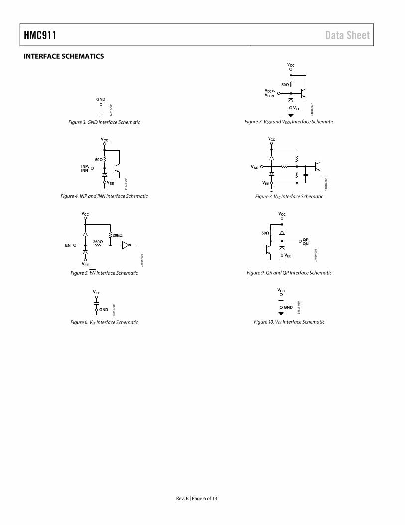
FREQUENCY (GHz)
0 2 4 6 8 10 12 14 1816 2220 24
RE
TU
RN
LO
SS
(d
B)
–45
–40
–35
–30
–25
–20
–15
–10
–5
0INNINP
VAC = 2.6VVDCN = 3.3VVCC = 3.3V
14
816
-02
9
Figure 29. Input Return Loss vs. Frequency,
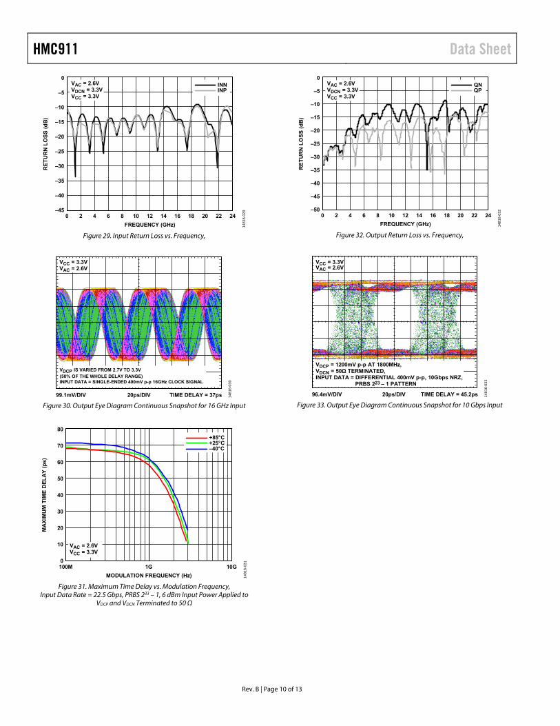
99.1mV/DIV 20ps/DIV TIME DELAY = 37ps
VCC = 3.3VVAC = 2.6V
VDCP IS VARIED FROM 2.7V TO 3.3V
(50% OF THE WHOLE DELAY RANGE)INPUT DATA = SINGLE-ENDED 400mV p-p 16GHz CLOCK SIGNAL
148
16-
03
0
Figure 30. Output Eye Diagram Continuous Snapshot for 16 GHz Input
100M 1G 10G
MA
XIM
UM
TIM
E D
EL
AY
(p
s)
MODULATION FREQUENCY (Hz)
0
10
20
30
40
50
60
70
80
+85°C+25°C–40°C
VAC = 2.6VVCC = 3.3V
148
16-
03
1
Figure 31. Maximum Time Delay vs. Modulation Frequency, Input Data Rate = 22.5 Gbps, PRBS 233 – 1, 6 dBm Input Power Applied to
VDCP and VDCN Terminated to 50 Ω
FREQUENCY (GHz)
0 2 4 6 8 10 12 14 1816 2220 24
RE
TU
RN
LO
SS
(d
B)
–50
–45
–40
–35
–30
–25
–20
–15
–10
–5
0QNQP
VAC = 2.6VVDCN = 3.3VVCC = 3.3V
148
16-
03
2
Figure 32. Output Return Loss vs. Frequency,
96.4mV/DIV 20ps/DIV TIME DELAY = 45.2ps
VCC = 3.3VVAC = 2.6V
VDCP = 1200mV p-p AT 1800MHz,VDCN = 50Ω TERMINATED,INPUT DATA = DIFFERENTIAL 400mV p-p, 10Gbps NRZ,
PRBS 223 – 1 PATTERN
148
16-
03
3
Figure 33. Output Eye Diagram Continuous Snapshot for 10 Gbps Input

Data Sheet HMC911
Rev. B | Page 11 of 13
APPLICATIONS INFORMATION EVALUATION PRINTED CIRCUIT BOARD (PCB) Generate the evaluation PCB used in this application with proper RF circuit design techniques. Signal lines at the RF port must have 50 Ω impedance, and the package ground leads and exposed paddle must be connected directly to the ground plane similar to what is shown in Figure 34. Use a sufficient number
of via holes to connect the top and bottom ground planes. Mount the evaluation board to an appropriate heat sink. The evaluation PCB shown is available from Analog Devices, Inc., upon request.
148
16-0
35
Figure 34. 600-00070-00-1 (EVAL01-HMC911LC4B) Evaluation Board
Bill of Materials
Table 4. Component Description J1 to J4 K connectors J5, J6 SMA connectors J7, J8 SMA connectors for through calibration TP1 to TP6 DC test points C1, C3 to C6 1 nF capacitors, 0402 package C2, C7 to C10 0.1 μF capacitors, 0402 package C9 100 nF capacitor, 0402 package C11 to C14 4.7 μF tantalum capacitors U1 HMC911 analog phase shifter PCB 600-00070-00-1 (EVAL01-HMC911LC4B1) evaluation PCB, circuit board material: Rogers 4350 or Arlon 25 FR
1 Reference this number when ordering the completed evaluation PCB.

HMC911 Data Sheet
Rev. B | Page 12 of 13
TYPICAL APPLICATION CIRCUIT Figure 35 shows the typical application circuit. Note that TP2 goes to ground and is not shown in Figure 35.
C114.7µF
C20.1µF
C11nF
VCCTP6
136
5 14
4 15
3 16
2 17
1 18
7 8 9 10 11 12192021222324
C144.7µF
C100.1µF
C51nF
VEETP3
C9100nF
C61nF
ENTP1
INPJ1
INNJ2
QPJ3
QNJ4
C124.7µF
C80.1µF
C31nF
VACTP5
C134.7µF
C70.1µF
C41nF
VEETP4
VDCPJ5
VDCNJ6
TEMPERATURECOMPENSATION
AND BIAS
VCC
VCC
VCC
VCC
AMP BUF
BUF
HMC911
14
816-
03
4
Figure 35. Typical Application Circuit

Data Sheet HMC911
Rev. B | Page 13 of 13
OUTLINE DIMENSIONS
12
0.50BSC
2.50 REFBOTTOM VIEWTOP VIEW
SIDE VIEW
SEATINGPLANE
1.02 MAX
2.50 SQ
1
24
7
13
18
19
6
FOR PROPER CONNECTION OFTHE EXPOSED PAD, REFER TOTHE PIN CONFIGURATION ANDFUNCTION DESCRIPTIONSSECTION OF THIS DATA SHEET.
04-0
3-2
015
-A
0.360.300.24
PIN 1(0.32 × 0.32)
EXPOSEDPAD
PK
G-0
00
00
0
PIN 1INDICATOR
4.134.00 SQ3.87
3.10 BSC
Figure 36. 24-Terminal Ceramic Leadless Chip [LCC]
(E-24-1) Dimensions shown in millimeters
ORDERING GUIDE
Model1 Temperature Range Package Body Material Lead Finish MSL Rating2 Package Description
Package Option
HMC911LC4B −40°C to +85°C Alumina, White Gold over Nickel MSL3 24-Terminal LCC E-24-1 HMC911LC4BTR −40°C to +85°C Alumina, White Gold over Nickel MSL3 24-Terminal LCC E-24-1 HMC911LC4BTR-R5 −40°C to +85°C Alumina, White Gold over Nickel MSL3 24-Terminal LCC E-24-1 EVAL01-HMC911LC4B Evaluation Board 1 The HMC911LC4B, HMC911LC4BTR, and HMC911LC4BTR-R5 are RoHS Compliant Parts. 2 See the Absolute Maximum Ratings section for additional information.
©2014–2016 Analog Devices, Inc. All rights reserved. Trademarks and registered trademarks are the property of their respective owners. D14816-0-10/16(B)