Embed Size (px)
Citation preview
1
Data Conversion and Lab (17.368)
Fall 2013
Lecture Outline
Class # 03
September 19, 2013
Dohn Bowden
2
Today’s Lecture Outline
• Administrative
• Detailed Technical Discussions
– Sample and Hold
• Lab
– Finish Lab #1– Conduct Lab #2
• Homework

3
Course Admin
4
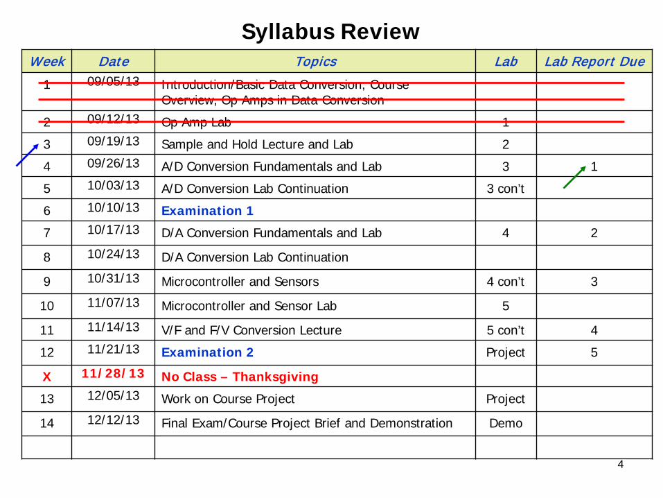
Syllabus ReviewWeek Date Topics Lab Lab Report Due
1 09/05/13 Introduction/Basic Data Conversion, Course Overview, Op Amps in Data Conversion
2 09/12/13 Op Amp Lab 1
3 09/19/13 Sample and Hold Lecture and Lab 2
4 09/26/13 A/D Conversion Fundamentals and Lab 3 1
5 10/03/13 A/D Conversion Lab Continuation 3 con’t
6 10/10/13 Examination 1
7 10/17/13 D/A Conversion Fundamentals and Lab 4 2
8 10/24/13 D/A Conversion Lab Continuation
9 10/31/13 Microcontroller and Sensors 4 con’t 3
10 11/07/13 Microcontroller and Sensor Lab 5
11 11/14/13 V/F and F/V Conversion Lecture 5 con’t 4
12 11/21/13 Examination 2 Project 5
X 11/28/13 No Class – Thanksgiving
13 12/05/13 Work on Course Project Project
14 12/12/13 Final Exam/Course Project Brief and Demonstration Demo
5
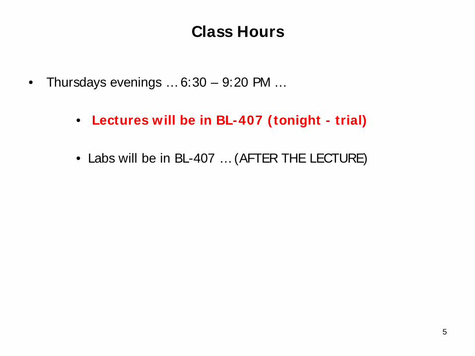
Class Hours
• Thursdays evenings … 6:30 – 9:20 PM …
• Lectures will be in BL-407 (tonight - trial)
• Labs will be in BL-407 … (AFTER THE LECTURE)

6
Email Distribution List
• I have STILL not received an email from some of you …
– If you have not done so already … Email me at …
7
Detailed Technical Discussion

8
References …
9
References
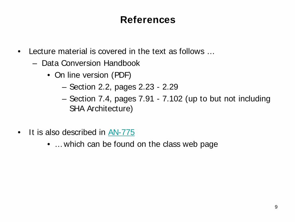
• Lecture material is covered in the text as follows …– Data Conversion Handbook
• On line version (PDF)– Section 2.2, pages 2.23 - 2.29– Section 7.4, pages 7.91 - 7.102 (up to but not including
SHA Architecture)
• It is also described in AN-775• … which can be found on the class web page
10
Sample and Hold …
11
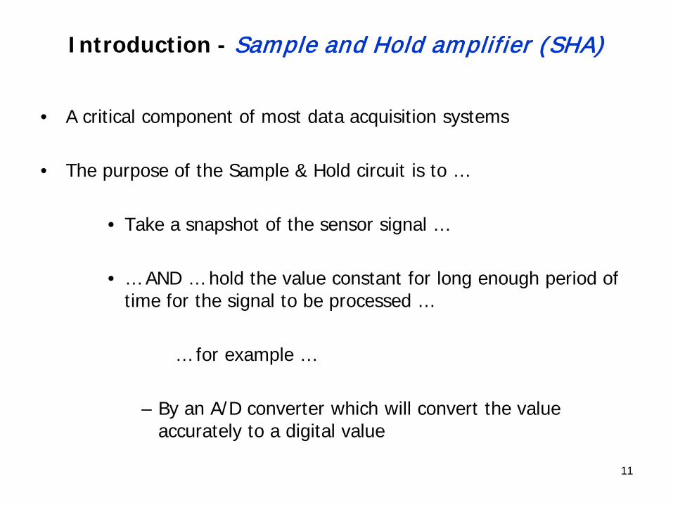
Introduction - Sample and Hold amplifier (SHA)
• A critical component of most data acquisition systems
• The purpose of the Sample & Hold circuit is to …
• Take a snapshot of the sensor signal …
• … AND … hold the value constant for long enough period of time for the signal to be processed …
… for example …
– By an A/D converter which will convert the value accurately to a digital value
12
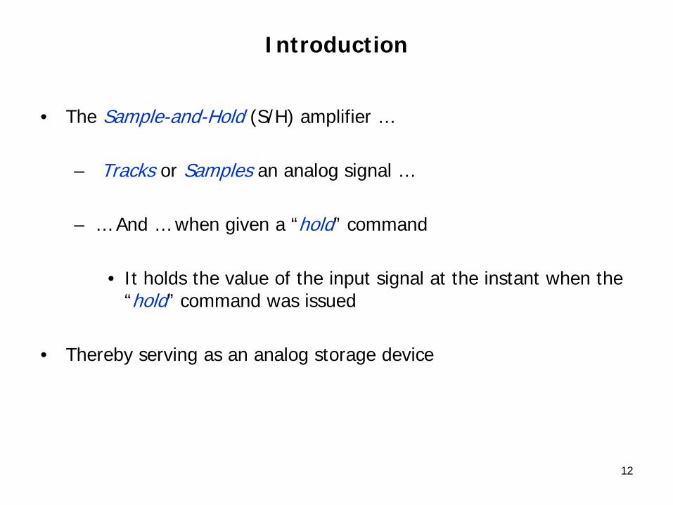
Introduction
• The Sample-and-Hold (S/H) amplifier …
– Tracks or Samples an analog signal …
– … And … when given a “hold” command
• It holds the value of the input signal at the instant when the “hold” command was issued
• Thereby serving as an analog storage device
13
Track and Hold … Sample and Hold
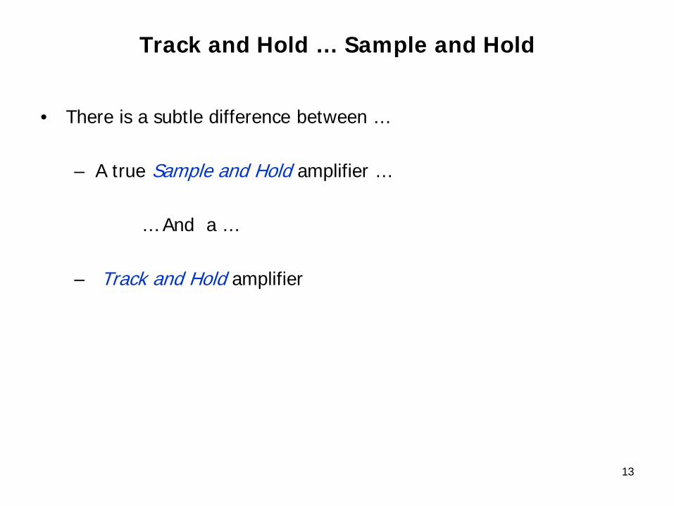
• There is a subtle difference between …
– A true Sample and Hold amplifier …
… And a …
– Track and Hold amplifier
14
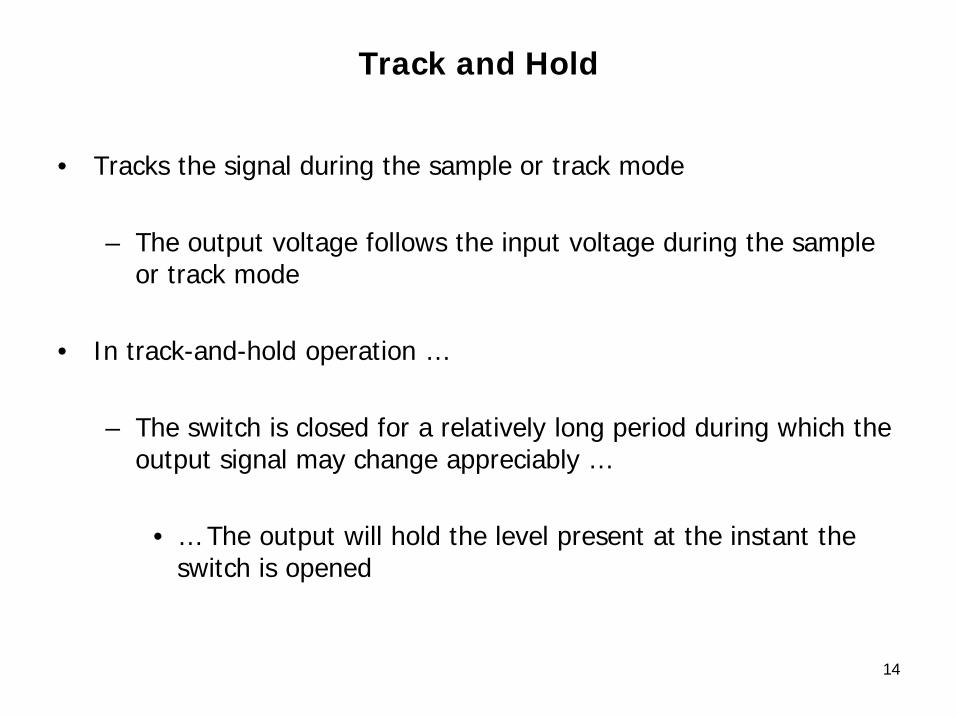
Track and Hold
• Tracks the signal during the sample or track mode
– The output voltage follows the input voltage during the sample or track mode
• In track-and-hold operation …
– The switch is closed for a relatively long period during which the output signal may change appreciably …
• … The output will hold the level present at the instant the switch is opened

15
Sample and Hold
• Samples the signal during the sample mode
• In sample-and-hold operation …
– … The switch is closed only for the period of time necessary to fully charge the holding capacitor
16
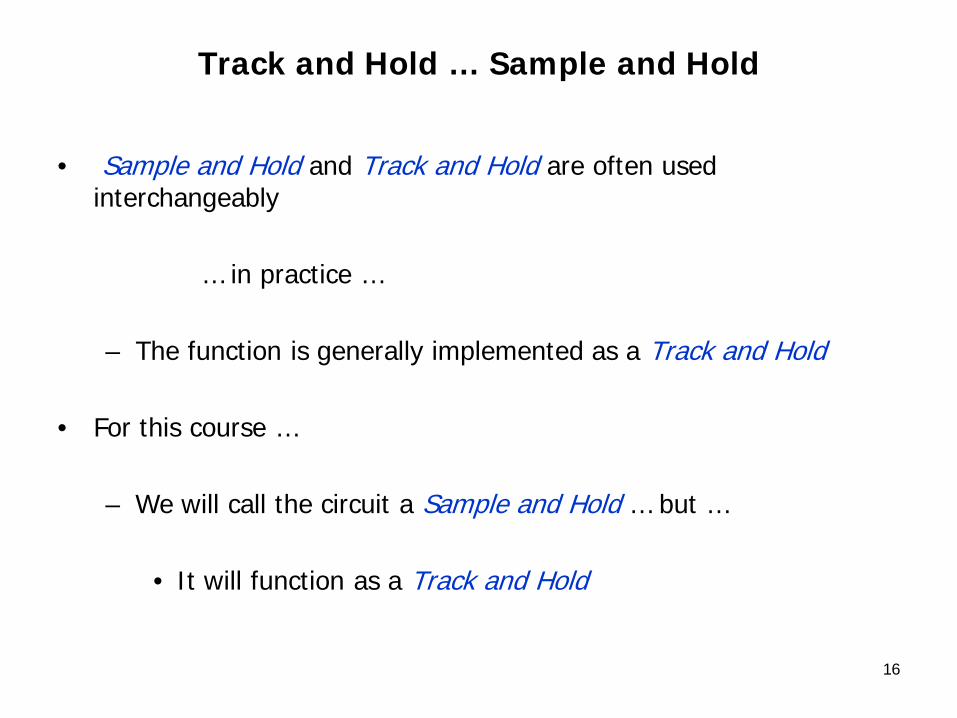
Track and Hold … Sample and Hold
• Sample and Hold and Track and Hold are often used interchangeably
… in practice …
– The function is generally implemented as a Track and Hold
• For this course …
– We will call the circuit a Sample and Hold … but …
• It will function as a Track and Hold
17
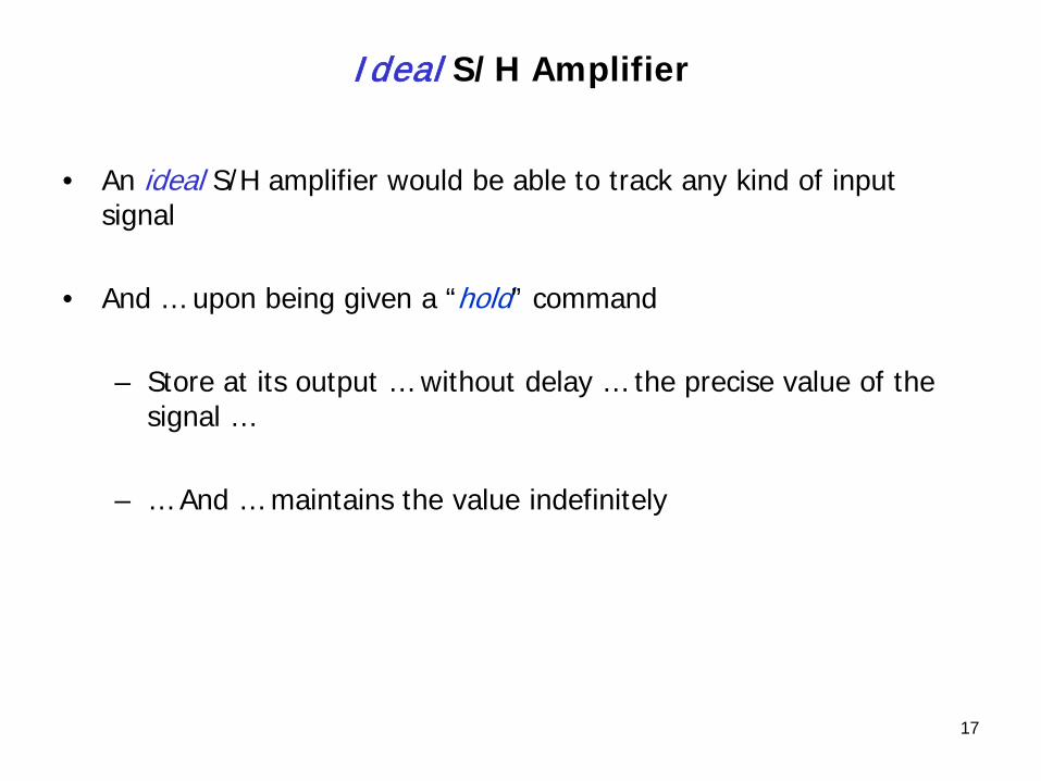
Ideal S/H Amplifier
• An ideal S/H amplifier would be able to track any kind of input signal
• And … upon being given a “hold” command
– Store at its output … without delay … the precise value of the signal …
– … And … maintains the value indefinitely

18
Input signal and SHA output signal
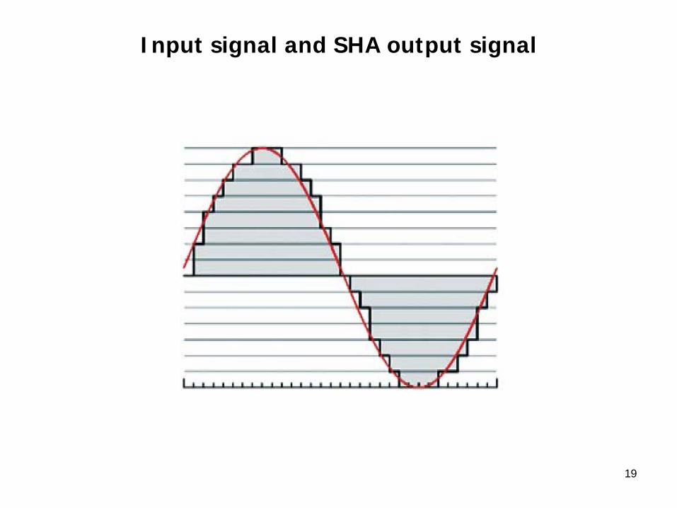
19
Input signal and SHA output signal
20
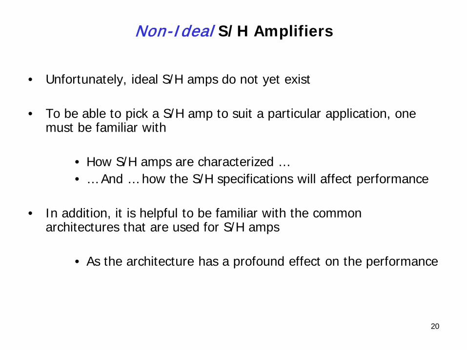
Non-Ideal S/H Amplifiers
• Unfortunately, ideal S/H amps do not yet exist
• To be able to pick a S/H amp to suit a particular application, one must be familiar with
• How S/H amps are characterized … • … And … how the S/H specifications will affect performance
• In addition, it is helpful to be familiar with the common architectures that are used for S/H amps
• As the architecture has a profound effect on the performance
21
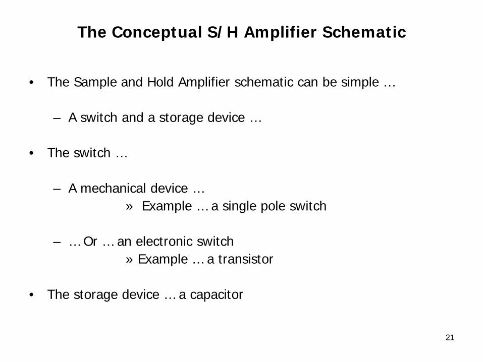
The Conceptual S/H Amplifier Schematic
• The Sample and Hold Amplifier schematic can be simple …
– A switch and a storage device …
• The switch …
– A mechanical device …» Example … a single pole switch
– … Or … an electronic switch» Example … a transistor
• The storage device … a capacitor
22
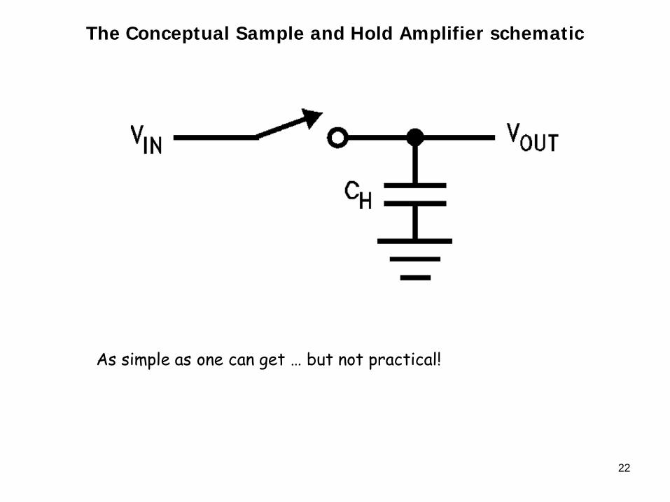
The Conceptual Sample and Hold Amplifier schematic
As simple as one can get … but not practical!

23
S/H Modes and Transitions Between the Modes
• Sample and Hold Amplifier has two modes …
• The sample mode
• The hold mode
• And two transitions between modes …
• Sample – to - Hold
• Hold – to - Sample
24
Sample Mode
• The switch is closed
• The voltage on the Hold Capacitor follows or tracks the input signal
25
Hold Mode
• The switch is open
• The Hold Capacitor retains the voltage present before it was disconnected
26
Sample-to-Hold Transition
• The switch goes from Sample-to-Hold
• Which is the switch going from closed to open
27
Hold-to-Sample Transition
• The switch goes from Hold-to-Sample
• Which is the switch going from open to closed
28
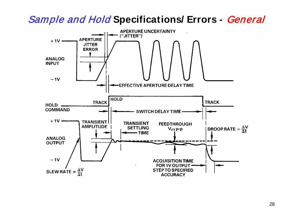
Sample and Hold Specifications/Errors - General

29
Sample Mode Specifications …

30
Sample Mode Specifications - General
• Sample mode is simply an amplifier circuit …• The specifications are similar to any amplifier … namely:
– Static» Offset» Gain» Nonlinearity
– Dynamic» Bandwidth» Slew Rate» Settling Time» Distortion **» Noise **
** Of a lesser interest than in the Hold ModeFor items not discussed … refer to Application Note (AN-775)

31
Sample Mode Specifications – Offset Voltage
• Offset Voltage VOS …
– Is the deviation from zero of the output voltage when the input voltage is zero and the S/H amp is in sample mode
– To maintain absolute accuracy in an A/D converter application, the offset voltage must be less than ½ LSB, or
– Where …• LSB is Least Significant Bit• FS is Full Scale• n is the resolution of the converter (number of bits)

32
Sample Mode Specifications – Gain
– Gain Error …
• Is the fractional voltage difference between the input voltage and the output voltage when the S/H amp is in sample mode
• Here we assume the ideal gain is unity
• If absolute accuracy is required in an A/D application, the gain error should be less than ½ LSB, or …
– Where …• LSB is Least Significant Bit• n is the resolution of the converter (number of bits)

33
Sample Mode Specifications – Slew Rate
• Slew Rate … The maximum rate of change of the output voltage when in the sample mode …
• The slew rate depends on the value of the hold capacitor …
– … This capacitance must be specified if the hold capacitor is external to the device
• Increasing the hold capacitor …
» Reduces the slew rate
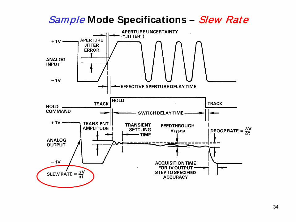
34
Sample Mode Specifications – Slew Rate
35
Hold Mode Specifications …

36
Hold Mode Specifications - General
• The specifications are …
– Static» Droop» Dielectric» Absorption
– Dynamic» Feedthrough» Distortion» Noise
For items not discussed … refer to Application Note (AN-775)

37
Hold Mode Specifications - General
• In conjunction with sampling … the device needs to be able to “hold” the signal for a finite amount of time … why? …
– During the “hold” time … the ADC will perform its function of converting the signal from analog to a digital value
38
Hold Mode Specifications - General
• The “hold” is performed via a storage capacitor
• Up to the time the “hold” is commanded … the capacitor is tracking/sampling the signal

39
Hold Mode Specifications - General
• During the hold mode there are errors due to imperfections
• Where are some of the imperfections be from?
• The hold capacitor
• The switch
• The output amplifier
40
Hold Mode Specifications - The Hold Capacitor
• If leakage current flows in or out of the capacitor …
… it will slowly charge or discharge the capacitor
… causing the voltage to change
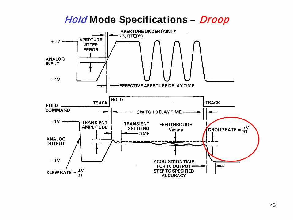
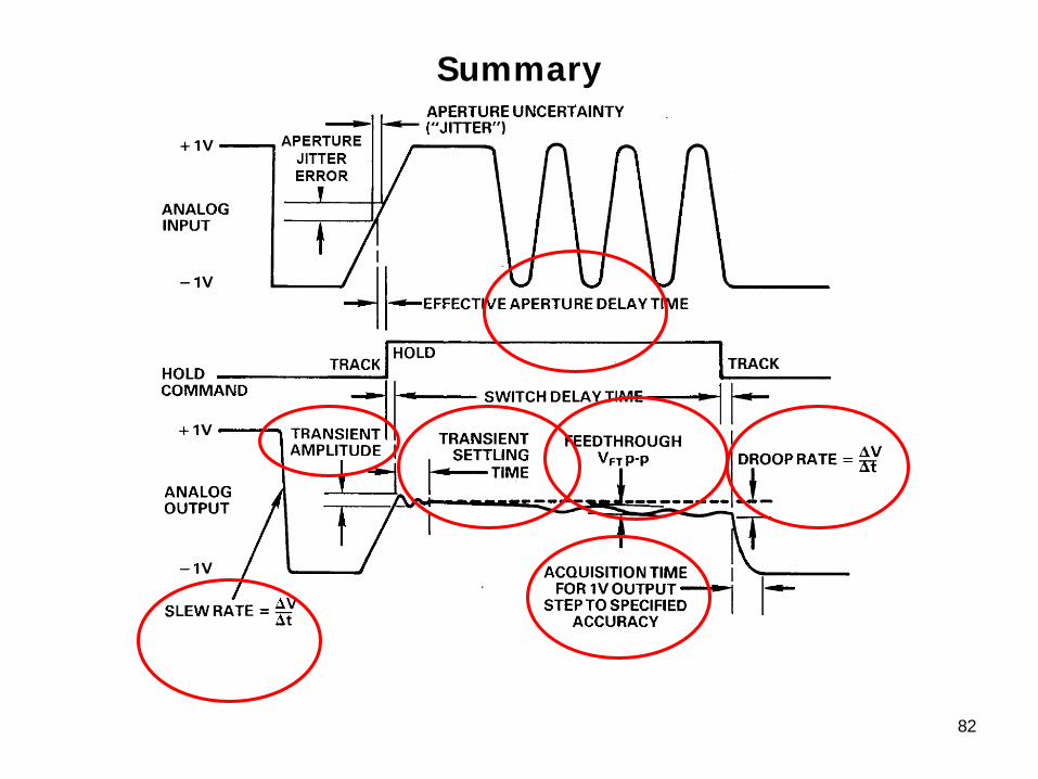
• This effect is known as droop
• An acceptable level of droop is …
– When the output of the SHA does not change by more than ½ LSB during the conversion time of the ADC it is driving

41
Hold Mode Specifications - Droop
42
Hold Mode Specifications - Droop
• The droop rate can be reduced by …
– Increasing the value of the hold capacitor
… but …
– This results in a higher acquisition time
43
Hold Mode Specifications – Droop
44
Hold Mode Specifications – Feedthrough
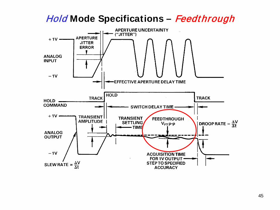
• Feedthrough - Another effect of the non-ideal switch …
– Charge is transferred from or to the hold capacitor by the circuits comprising the switch … known as …
• signal feedthrough
45
Hold Mode Specifications – Feedthrough
46
Sample – to – Hold Mode Specifications
47
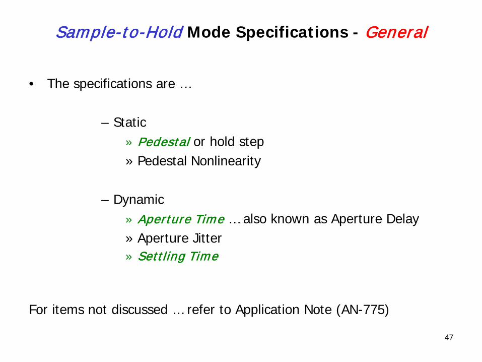
Sample-to-Hold Mode Specifications - General
• The specifications are …
– Static» Pedestal or hold step» Pedestal Nonlinearity
– Dynamic» Aperture Time … also known as Aperture Delay » Aperture Jitter» Settling Time
For items not discussed … refer to Application Note (AN-775)
48
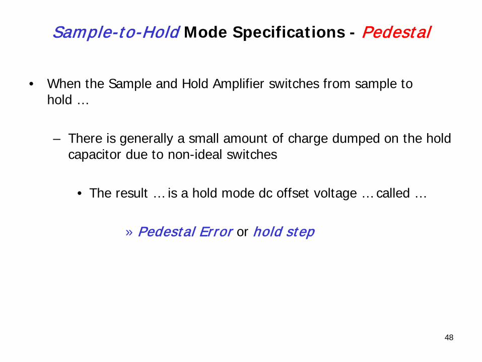
Sample-to-Hold Mode Specifications - Pedestal
• When the Sample and Hold Amplifier switches from sample to hold …
– There is generally a small amount of charge dumped on the hold capacitor due to non-ideal switches
• The result … is a hold mode dc offset voltage … called …
» Pedestal Error or hold step

49
Sample-to-Hold Mode Specifications - Pedestal

50
Sample-to-Hold Mode Specifications - Pedestal
Pedestal
51
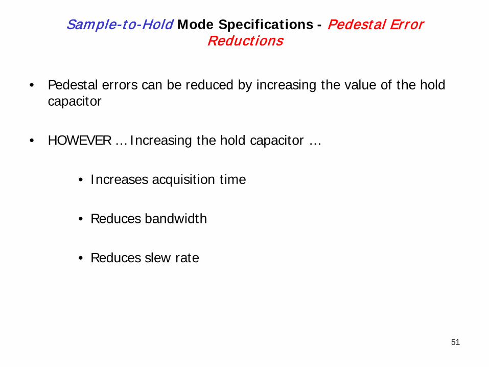
Sample-to-Hold Mode Specifications - Pedestal Error Reductions
• Pedestal errors can be reduced by increasing the value of the hold capacitor
• HOWEVER … Increasing the hold capacitor …
• Increases acquisition time
• Reduces bandwidth
• Reduces slew rate
52
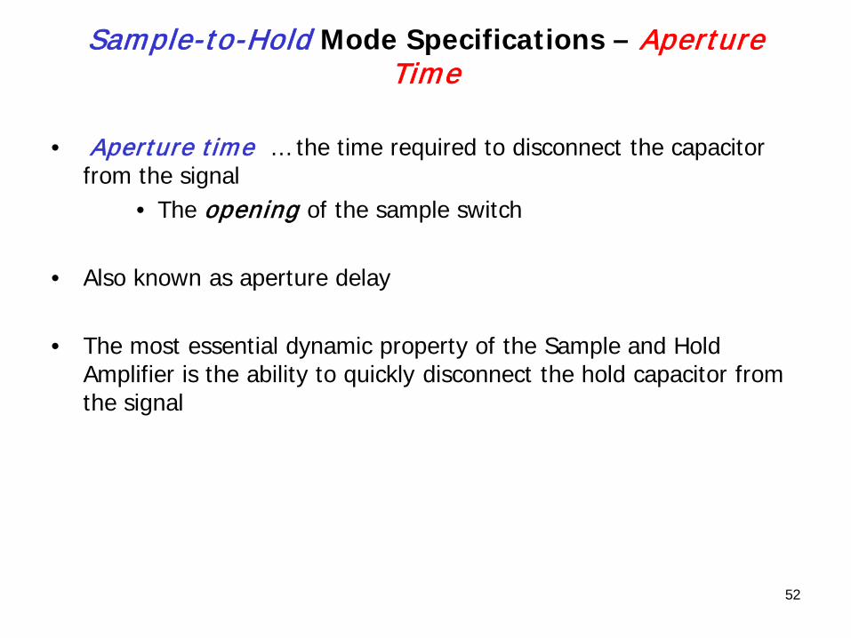
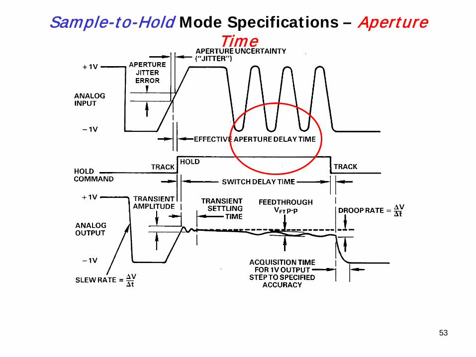
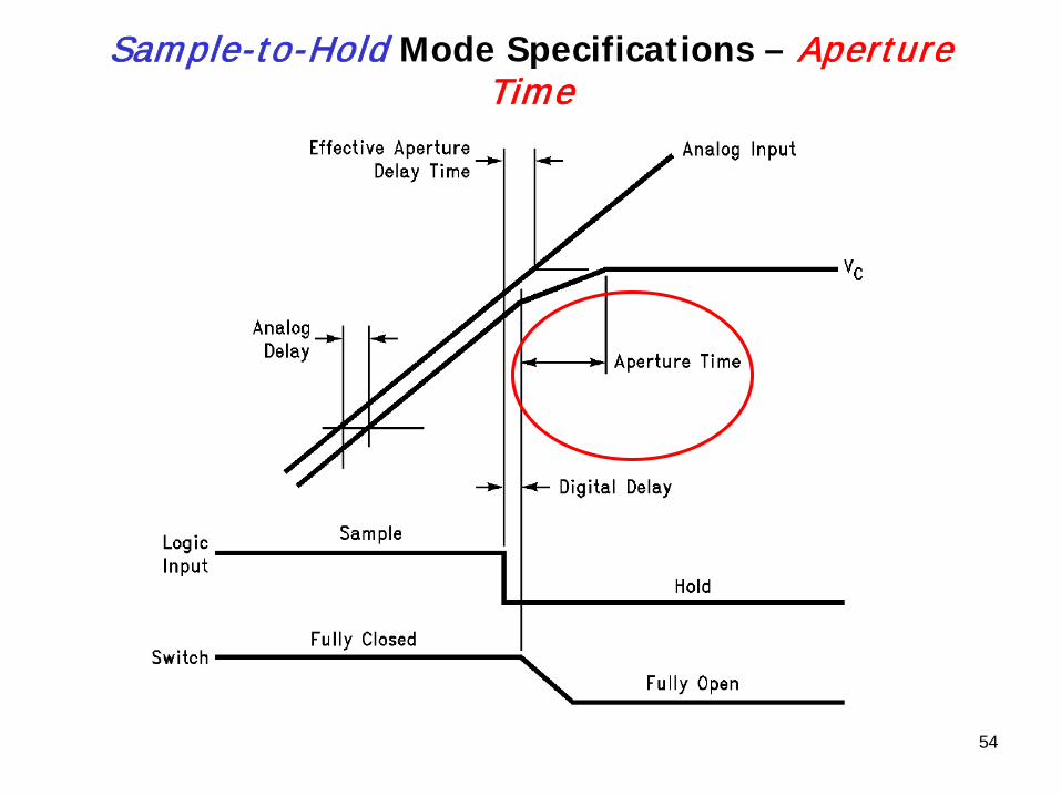
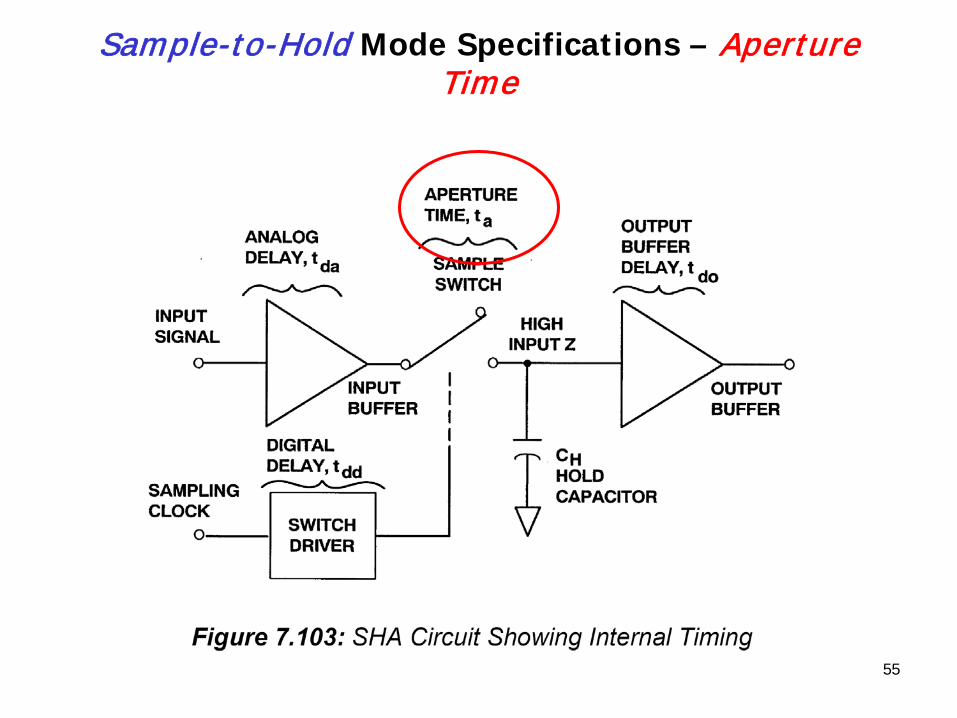
Sample-to-Hold Mode Specifications – Aperture Time
• Aperture time … the time required to disconnect the capacitor from the signal
• The opening of the sample switch
• Also known as aperture delay
• The most essential dynamic property of the Sample and Hold Amplifier is the ability to quickly disconnect the hold capacitor from the signal
53
Sample-to-Hold Mode Specifications – Aperture Time
54
Sample-to-Hold Mode Specifications – Aperture Time
55
Sample-to-Hold Mode Specifications – Aperture Time

56
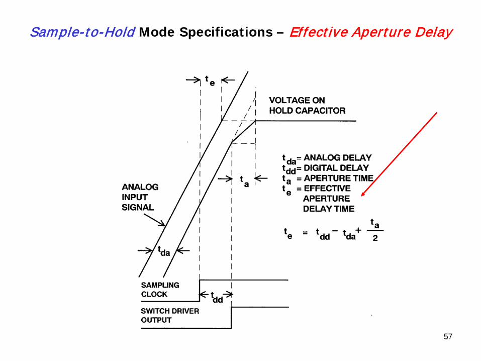
Sample-to-Hold Mode Specifications – Effective Aperture Delay
• Effective Aperture Delay time is …
– The time delay between the generation of the hold command… and …
– The appearance at the input of the final “held”' voltage that exists on the hold capacitor
• If precise timing is required …
– The hold command must be given an “effective aperture delay time” before the instant at which the input value is desired
57
Sample-to-Hold Mode Specifications – Effective Aperture Delay

58
Sample-to-Hold Mode Specifications – Effective Aperture Delay
• Aperture delay produces no errors … but …
• Acts as a fixed delay …
– Either in the sampling clock input or the analog input (depends on the sign)

59
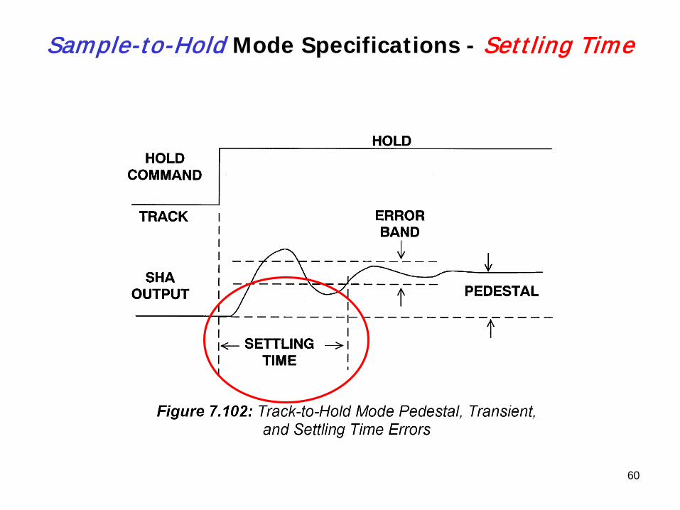
Sample-to-Hold Mode Specifications – Settling Time
• The time required for the output to settle within a specified error band after a hold command has been given
60
Sample-to-Hold Mode Specifications - Settling Time

61
Sample-to-Hold Mode Specifications - Settling Time
62
Sample-to-Hold Mode Specifications – Final Held Value
• The actual value of the voltage that is held … is a function of …
– The input signal … and …
– The errors introduced by the switching operation
• The “held” value is …
– A delayed version of the input …
– Averaged over the aperture time

63
Hold – to – SampleMode Specifications
64
Hold-to-Sample Mode Specifications - General
• The specifications are …
– Static:» None
– Dynamic:» Acquisition Time» Sw itching Transient
65
Hold-to-Sample Transition Specifications - Acquisition time
• When the Sample to Hold Amplifier switches from the hold mode to the sample mode
– It must reacquire the input signal
• The time it takes to reacquire the signal is the Acquisition time
• Acquisition time is the time required to reacquire the signal to the desired accuracy when switching from hold to sample
– The interval starts at 50% point of the sampling clock edge
– It ends when the voltage falls to within specification

66
Hold-to-Sample Mode Specifications – Acquisition Time
67
Hold-to-Sample Transition Specifications - Acquisition time
• Acquisition Time is the maximum time required to acquire a new input voltage once a sample command has been given
• A signal is “acquired” when it has settled within a specified error band around its final value of output voltage
• Acquisition Time … is the time for the hold capacitor to charge up to the VIN value

68
Acquisit ion Time
69
Hold-to-Sample Transition Specifications - Acquisition time
• The maximum value of the acquisition time occurs when the hold capacitor must charge to a full-scale voltage change
• The acquisition time depends on the value of the hold capacitor
– The acquisition time can be reduced by choosing a smaller hold capacitance
… however …
– … this will increase the hold step and droop rate
70
Hold-to-Sample Transition Specifications – Sw itching Transient
• The transient that appears at the output due to the transition
– Can be either Sample to Hold or Hold to Sample
• The maximum amplitude of the transient is usually specified
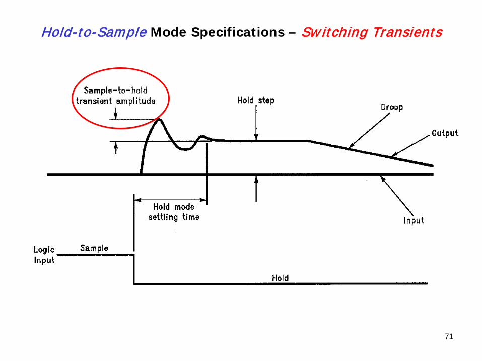
71
Hold-to-Sample Mode Specifications – Sw itching Transients

72
Sample and Hold Architectures
73
Sample and Hold Architectures
• The text discusses a variety of architectures starting on …
– page 529 of the Textbook (page 7.102 online version)
– as well as Application Note (AN-775)
• The following are the basis for the various types …

74
Practical basic Sample and Hold Amplifier schematics
VIN VOUT

75
Practical Sample and Hold circuit
• The input buffer …
… Provides high impedance to the signal source
… And provides current gain to charge the capacitor
• The output buffer …
… Provides high input impedance to the hold capacitor …
… to help the voltage from being discharged prematurely
• The switching circuit and its driver signal …
… forms the mechanism by which the hold capacitor is switched between Sample & Hold

76
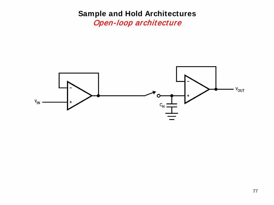
Sample and Hold ArchitecturesOpen-loop architecture
• The input and output buffer amps are each configured as buffers
• The advantage of this architecture is its speed …
– The acquisition time and settling time are short because there is no feedback between the buffer amps
• The disadvantage of this architecture is in its accuracy, which suffers because of the lack of feedback, causing the dc errors of both amplifiers to add
77
Sample and Hold ArchitecturesOpen-loop architecture
78
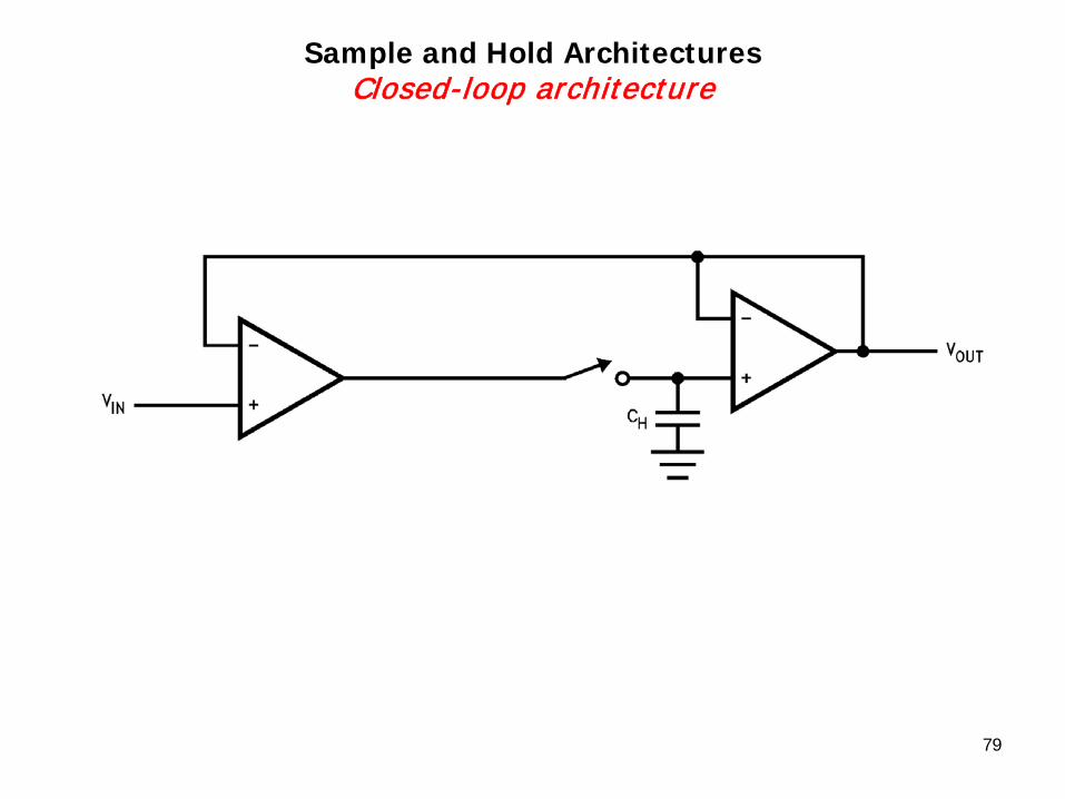
Sample and Hold ArchitecturesClosed-loop architecture
• For applications requiring high accuracy …
– Use the closed loop-architecture
• The feedback significantly improves the accuracy of the S/H relative to the open-loop configuration …
– Although the speed is somewhat less
79
Sample and Hold ArchitecturesClosed-loop architecture
80
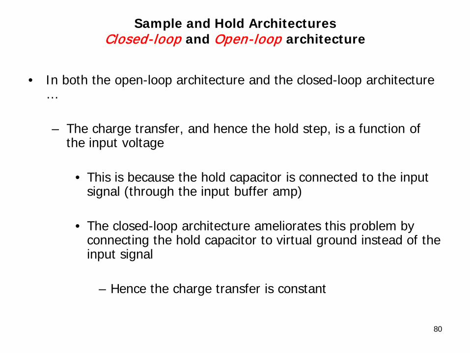
Sample and Hold ArchitecturesClosed-loop and Open-loop architecture
• In both the open-loop architecture and the closed-loop architecture …
– The charge transfer, and hence the hold step, is a function of the input voltage
• This is because the hold capacitor is connected to the input signal (through the input buffer amp)
• The closed-loop architecture ameliorates this problem by connecting the hold capacitor to virtual ground instead of the input signal
– Hence the charge transfer is constant
81
Summary …
82
Summary

83
Lab

84
Lab #2 …
85
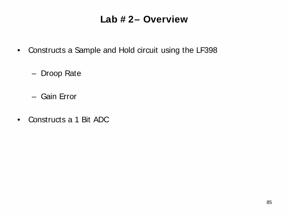
Lab #2– Overview
• Constructs a Sample and Hold circuit using the LF398
– Droop Rate
– Gain Error
• Constructs a 1 Bit ADC

86
Next Class
87
Next Class Topics
• A/D Conversion Fundamentals
• Start Lab #3

88
Homework
89
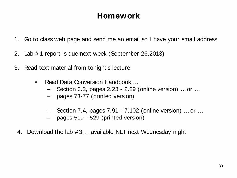
Homework
1. Go to class web page and send me an email so I have your email address
2. Lab #1 report is due next week (September 26,2013)
3. Read text material from tonight's lecture
• Read Data Conversion Handbook …– Section 2.2, pages 2.23 - 2.29 (online version) … or …– pages 73-77 (printed version)
– Section 7.4, pages 7.91 - 7.102 (online version) … or …– pages 519 - 529 (printed version)
4. Download the lab #3 … available NLT next Wednesday night
90
Time to start the lab …
Lab
• Lab #2 …
• Your thoughts on the lecture in this room (BL-407)????
91
92
Questions?
93
References …
94
References
1. None