Embed Size (px)
Citation preview
Computational Materials Science 65 (2012) 470–484
Contents lists available at SciVerse ScienceDirect
Computational Materials Science
journal homepage: www.elsevier .com/locate /commatsci
Damage of lead-free solder joints in flip chip assemblies subjectedto high-temperature thermal cycling
Emeka H. Amalu ⇑, N.N. EkereElectronics Manufacturing Engineering Research Group, School of Engineering at Medway, University of Greenwich, Chatham Maritime, Kent ME4 4TB, UK
a r t i c l e i n f o
Article history:Received 8 June 2012Received in revised form 24 July 2012Accepted 3 August 2012Available online 15 September 2012
Keywords:High-temperature electronicsInter-metallic compoundsLead-free solderFlip chipSolder joint reliabilitySolder joint damage
0927-0256/$ - see front matter � 2012 Elsevier B.V. Ahttp://dx.doi.org/10.1016/j.commatsci.2012.08.005
⇑ Corresponding author. Tel.: +44 (0)1634883873;E-mail addresses: [email protected]
(E.H. Amalu).
a b s t r a c t
The damage mechanism of lead-free ball grid array (BGA) solder joints is studied whilst the magnitude ofthe damage was quantitatively evaluated to determine the impact of the thickness of inter-metallic com-pound (IMC) layer on the reliability of the joints. Five virtual test vehicle assemblies of flip chip (FC)which have 4–12 lm thickness of IMC layer were subjected to the same accelerated high-temperaturecycles utilising, in parts, the IEC standard 60749-25. The visco-plastic responses of the assemblies’ solderbump joints to the induced thermal load were simulated using Anand’s plasticity model. The results dem-onstrate that very thin and thick thickness of IMC layer impact the reliability of the FC solder joints. It wasfound that strain range at steady state joint damage is approximately 0.07–0.12. This finding indicatesthat strain controlled studies on bulk solder which are not up to these limits are inadequate to charac-terise damage behaviour and model damage evolution in the FC BGA solder bump joints. Further resultsshow that the magnitude of the average accumulated visco-plastic energy density per cycle (wacc)depends on the volume percentage of solder and IMC in the joints. This dependency explains why theexisting life prediction models based on wacc are not satisfactory in estimating the damage in solderjoints. The authors propose the development of new prediction models which will be specific on the vol-ume percentage of solder and IMC in the joints.
� 2012 Elsevier B.V. All rights reserved.
1. Introduction
Solder joints in electronic devices are one of the key compo-nents of the assemblies whose reliability concern increases at ele-vated temperature of operations due to the growth of inter-metallic compound (IMC) in the joints and also the accelerateddegradation of the solder alloys. In high-temperature electronics(HTE), solder joints observe increased thermal energy arising fromboth extensive high-temperature excursions and the dissipation ofexcess heat the chip generated during operations. The long opera-tions of HTE continues to grow IMC at its solder joints because thesolder and metalized copper bond pad continually engage in solidstate reaction until copper content in bond pad is depleted. Evenwith good heat dissipation mechanism (application of good ther-mal interface materials and heat spreader system) significantamount of heat still flow through the solder joints and activatesdiffusion of elements which culminates in the growth of the IMClayer. Peng et al. [1] reported that the thickness of Cu3Sn andCu6Sn5 IMCs in their SnAgCu solder joints increased with agingtime and Laurila et al. [2] reported an enhanced growth of IMC in
ll rights reserved.
fax: +44 (0)1634883153., [email protected]
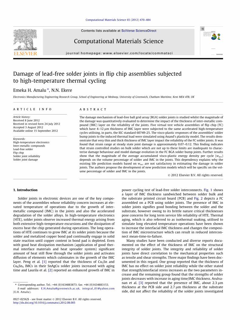
power cycling test of lead-free solder interconnects. Fig. 1 showsa layer of IMC thickness sandwiched between solder bulk andthe substrate printed circuit board (PCB) and Fig. 2 depicts a FCassembled on a PCB using solder joints. The presence of IMC insolder joints signifies good bonding between the solder and thesubstrate, however owing to its brittle nature critical thicknessespose concerns for long term service life reliability of HTE. Thermalaging, which is also referred to as isothermal soaking, utilised tosimulate long elevated temperature operations have been shownto increase the interfacial IMC thickness and changes the composi-tion of IMC microstructure which can result in reduced intercon-nect mean-time-to-failure.
Many studies have been conducted and diverse reports docu-mented on the effect of the thickness of IMC on the structuralintegrity of solder joints. The integrity and reliability of solderjoints have direct correlation to the mechanical properties suchas tensile and shear strengths. Three major findings have been doc-umented in this regard. One group reported that the thickness ofIMC has no effect on solder joint reliability while the other statedthat strength/interfacial stress increases as the two parameters in-crease and the remaining group found that the strengths of solderjoints decreases with increase in aging time/IMC thickness. Arulva-nan et al. [3] reported that the presence of IMC, about 2.3 lmthickness at the PCB side and 2.7 lm thickness at the substrateside, did not affect the reliability of the solder joints investigated
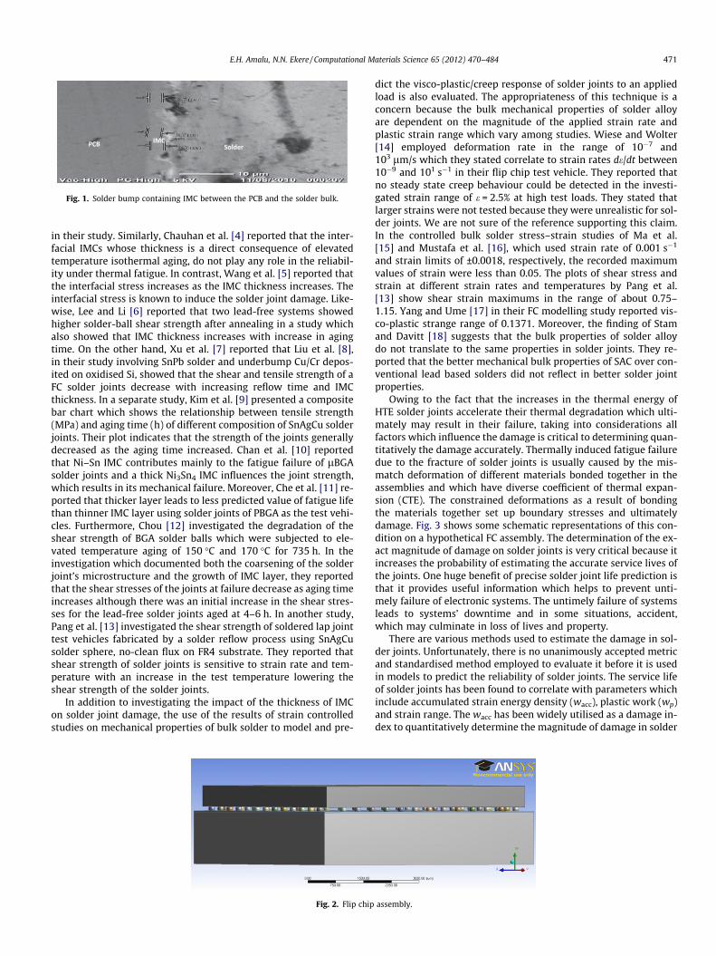
Fig. 1. Solder bump containing IMC between the PCB and the solder bulk.
E.H. Amalu, N.N. Ekere / Computational Materials Science 65 (2012) 470–484 471
in their study. Similarly, Chauhan et al. [4] reported that the inter-facial IMCs whose thickness is a direct consequence of elevatedtemperature isothermal aging, do not play any role in the reliabil-ity under thermal fatigue. In contrast, Wang et al. [5] reported thatthe interfacial stress increases as the IMC thickness increases. Theinterfacial stress is known to induce the solder joint damage. Like-wise, Lee and Li [6] reported that two lead-free systems showedhigher solder-ball shear strength after annealing in a study whichalso showed that IMC thickness increases with increase in agingtime. On the other hand, Xu et al. [7] reported that Liu et al. [8],in their study involving SnPb solder and underbump Cu/Cr depos-ited on oxidised Si, showed that the shear and tensile strength of aFC solder joints decrease with increasing reflow time and IMCthickness. In a separate study, Kim et al. [9] presented a compositebar chart which shows the relationship between tensile strength(MPa) and aging time (h) of different composition of SnAgCu solderjoints. Their plot indicates that the strength of the joints generallydecreased as the aging time increased. Chan et al. [10] reportedthat Ni–Sn IMC contributes mainly to the fatigue failure of lBGAsolder joints and a thick Ni3Sn4 IMC influences the joint strength,which results in its mechanical failure. Moreover, Che et al. [11] re-ported that thicker layer leads to less predicted value of fatigue lifethan thinner IMC layer using solder joints of PBGA as the test vehi-cles. Furthermore, Chou [12] investigated the degradation of theshear strength of BGA solder balls which were subjected to ele-vated temperature aging of 150 �C and 170 �C for 735 h. In theinvestigation which documented both the coarsening of the solderjoint’s microstructure and the growth of IMC layer, they reportedthat the shear stresses of the joints at failure decrease as aging timeincreases although there was an initial increase in the shear stres-ses for the lead-free solder joints aged at 4–6 h. In another study,Pang et al. [13] investigated the shear strength of soldered lap jointtest vehicles fabricated by a solder reflow process using SnAgCusolder sphere, no-clean flux on FR4 substrate. They reported thatshear strength of solder joints is sensitive to strain rate and tem-perature with an increase in the test temperature lowering theshear strength of the solder joints.
In addition to investigating the impact of the thickness of IMCon solder joint damage, the use of the results of strain controlledstudies on mechanical properties of bulk solder to model and pre-
Fig. 2. Flip chip
dict the visco-plastic/creep response of solder joints to an appliedload is also evaluated. The appropriateness of this technique is aconcern because the bulk mechanical properties of solder alloyare dependent on the magnitude of the applied strain rate andplastic strain range which vary among studies. Wiese and Wolter[14] employed deformation rate in the range of 10�7 and103 lm/s which they stated correlate to strain rates de/dt between10�9 and 101 s�1 in their flip chip test vehicle. They reported thatno steady state creep behaviour could be detected in the investi-gated strain range of e = 2.5% at high test loads. They stated thatlarger strains were not tested because they were unrealistic for sol-der joints. We are not sure of the reference supporting this claim.In the controlled bulk solder stress–strain studies of Ma et al.[15] and Mustafa et al. [16], which used strain rate of 0.001 s�1
and strain limits of ±0.0018, respectively, the recorded maximumvalues of strain were less than 0.05. The plots of shear stress andstrain at different strain rates and temperatures by Pang et al.[13] show shear strain maximums in the range of about 0.75–1.15. Yang and Ume [17] in their FC modelling study reported vis-co-plastic strange range of 0.1371. Moreover, the finding of Stamand Davitt [18] suggests that the bulk properties of solder alloydo not translate to the same properties in solder joints. They re-ported that the better mechanical bulk properties of SAC over con-ventional lead based solders did not reflect in better solder jointproperties.
Owing to the fact that the increases in the thermal energy ofHTE solder joints accelerate their thermal degradation which ulti-mately may result in their failure, taking into considerations allfactors which influence the damage is critical to determining quan-titatively the damage accurately. Thermally induced fatigue failuredue to the fracture of solder joints is usually caused by the mis-match deformation of different materials bonded together in theassemblies and which have diverse coefficient of thermal expan-sion (CTE). The constrained deformations as a result of bondingthe materials together set up boundary stresses and ultimatelydamage. Fig. 3 shows some schematic representations of this con-dition on a hypothetical FC assembly. The determination of the ex-act magnitude of damage on solder joints is very critical because itincreases the probability of estimating the accurate service lives ofthe joints. One huge benefit of precise solder joint life prediction isthat it provides useful information which helps to prevent unti-mely failure of electronic systems. The untimely failure of systemsleads to systems’ downtime and in some situations, accident,which may culminate in loss of lives and property.
There are various methods used to estimate the damage in sol-der joints. Unfortunately, there is no unanimously accepted metricand standardised method employed to evaluate it before it is usedin models to predict the reliability of solder joints. The service lifeof solder joints has been found to correlate with parameters whichinclude accumulated strain energy density (wacc), plastic work (wp)and strain range. The wacc has been widely utilised as a damage in-dex to quantitatively determine the magnitude of damage in solder
assembly.
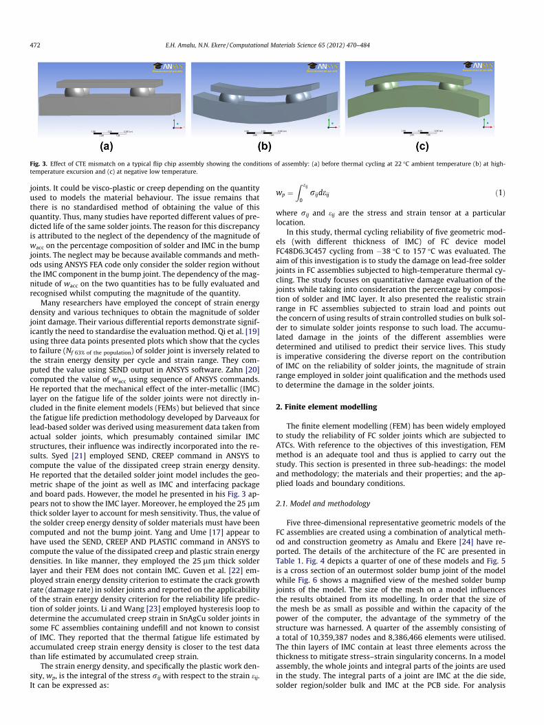
Fig. 3. Effect of CTE mismatch on a typical flip chip assembly showing the conditions of assembly: (a) before thermal cycling at 22 �C ambient temperature (b) at high-temperature excursion and (c) at negative low temperature.
472 E.H. Amalu, N.N. Ekere / Computational Materials Science 65 (2012) 470–484
joints. It could be visco-plastic or creep depending on the quantityused to models the material behaviour. The issue remains thatthere is no standardised method of obtaining the value of thisquantity. Thus, many studies have reported different values of pre-dicted life of the same solder joints. The reason for this discrepancyis attributed to the neglect of the dependency of the magnitude ofwacc on the percentage composition of solder and IMC in the bumpjoints. The neglect may be because available commands and meth-ods using ANSYS FEA code only consider the solder region withoutthe IMC component in the bump joint. The dependency of the mag-nitude of wacc on the two quantities has to be fully evaluated andrecognised whilst computing the magnitude of the quantity.
Many researchers have employed the concept of strain energydensity and various techniques to obtain the magnitude of solderjoint damage. Their various differential reports demonstrate signif-icantly the need to standardise the evaluation method. Qi et al. [19]using three data points presented plots which show that the cyclesto failure (Nf 63% of the population) of solder joint is inversely related tothe strain energy density per cycle and strain range. They com-puted the value using SEND output in ANSYS software. Zahn [20]computed the value of wacc using sequence of ANSYS commands.He reported that the mechanical effect of the inter-metallic (IMC)layer on the fatigue life of the solder joints were not directly in-cluded in the finite element models (FEMs) but believed that sincethe fatigue life prediction methodology developed by Darveaux forlead-based solder was derived using measurement data taken fromactual solder joints, which presumably contained similar IMCstructures, their influence was indirectly incorporated into the re-sults. Syed [21] employed SEND, CREEP command in ANSYS tocompute the value of the dissipated creep strain energy density.He reported that the detailed solder joint model includes the geo-metric shape of the joint as well as IMC and interfacing packageand board pads. However, the model he presented in his Fig. 3 ap-pears not to show the IMC layer. Moreover, he employed the 25 lmthick solder layer to account for mesh sensitivity. Thus, the value ofthe solder creep energy density of solder materials must have beencomputed and not the bump joint. Yang and Ume [17] appear tohave used the SEND, CREEP AND PLASTIC command in ANSYS tocompute the value of the dissipated creep and plastic strain energydensities. In like manner, they employed the 25 lm thick solderlayer and their FEM does not contain IMC. Guven et al. [22] em-ployed strain energy density criterion to estimate the crack growthrate (damage rate) in solder joints and reported on the applicabilityof the strain energy density criterion for the reliability life predic-tion of solder joints. Li and Wang [23] employed hysteresis loop todetermine the accumulated creep strain in SnAgCu solder joints insome FC assemblies containing undefill and not known to consistof IMC. They reported that the thermal fatigue life estimated byaccumulated creep strain energy density is closer to the test datathan life estimated by accumulated creep strain.
The strain energy density, and specifically the plastic work den-sity, wp, is the integral of the stress rij with respect to the strain eij.It can be expressed as:
wp ¼Z eij
0rijdeij ð1Þ
where rij and eij are the stress and strain tensor at a particularlocation.
In this study, thermal cycling reliability of five geometric mod-els (with different thickness of IMC) of FC device modelFC48D6.3C457 cycling from �38 �C to 157 �C was evaluated. Theaim of this investigation is to study the damage on lead-free solderjoints in FC assemblies subjected to high-temperature thermal cy-cling. The study focuses on quantitative damage evaluation of thejoints while taking into consideration the percentage by composi-tion of solder and IMC layer. It also presented the realistic strainrange in FC assemblies subjected to strain load and points outthe concern of using results of strain controlled studies on bulk sol-der to simulate solder joints response to such load. The accumu-lated damage in the joints of the different assemblies weredetermined and utilised to predict their service lives. This studyis imperative considering the diverse report on the contributionof IMC on the reliability of solder joints, the magnitude of strainrange employed in solder joint qualification and the methods usedto determine the damage in the solder joints.
2. Finite element modelling
The finite element modelling (FEM) has been widely employedto study the reliability of FC solder joints which are subjected toATCs. With reference to the objectives of this investigation, FEMmethod is an adequate tool and thus is applied to carry out thestudy. This section is presented in three sub-headings: the modeland methodology; the materials and their properties; and the ap-plied loads and boundary conditions.
2.1. Model and methodology
Five three-dimensional representative geometric models of theFC assemblies are created using a combination of analytical meth-od and construction geometry as Amalu and Ekere [24] have re-ported. The details of the architecture of the FC are presented inTable 1. Fig. 4 depicts a quarter of one of these models and Fig. 5is a cross section of an outermost solder bump joint of the modelwhile Fig. 6 shows a magnified view of the meshed solder bumpjoints of the model. The size of the mesh on a model influencesthe results obtained from its modelling. In order that the size ofthe mesh be as small as possible and within the capacity of thepower of the computer, the advantage of the symmetry of thestructure was harnessed. A quarter of the assembly consisting ofa total of 10,359,387 nodes and 8,386,466 elements were utilised.The thin layers of IMC contain at least three elements across thethickness to mitigate stress–strain singularity concerns. In a modelassembly, the whole joints and integral parts of the joints are usedin the study. The integral parts of a joint are IMC at the die side,solder region/solder bulk and IMC at the PCB side. For analysis
Table 1Parameters of flip chip architecture.
Bumps Bump matrix Pitch Die size(mm)
Bump size heightand diameter
Tray qty Lead-free SAC – Sn/Ag/Cuorder number
Ref Quick view
48 12�12 Perimeter 18mil 457 lm 6.3 mm 140 lm ø178 lm 25pcs waffle 200 FC48D6.3C457-DC FBT250
(a) (b)Fig. 4. A quarter of the flip chip assembly showing: (a) the assembly with two planes of symmetry and (b) the assembly with adequate mesh.
Fig. 5. A cross section of an outermost solder bump joint of the flip chip assembly.
Fig. 6. A meshed solder bump showing 6 lm thickness of IMC at both the die andPCB sides of the bump.
Fig. 7. Relationship between model number and inter-metallic compoundthickness.
E.H. Amalu, N.N. Ekere / Computational Materials Science 65 (2012) 470–484 473
purposes, a whole joint which consists of IMC at the die side, solderregion and IMC at the PCB side is simply called a bump. The solderregion is simply called solder and designated simply as ‘‘s’’ in anal-
ysis. Thus, its stress is denoted as rS. The bump or solder bump isdesignated simply as ‘‘B’’ in analysis. Similarly, its stress is desig-nated as rB. The thickness of the layer of IMC in the joints of themodels is different in different models. Thus, the five models haveIMC thickness of 4 lm, 6 lm, 8 lm, 10 lm and 12 lm. These mag-nitudes of IMC thickness are within the range reported by Georgeet al. [25] in their thermal cycling reliability of lead-free solder forhigh-temperature applications. The five assemblies were employedinstead of modelling the growth of the compound as the ATC pro-gresses because Arulvanan et al. [3] have reported that IMC growthwas about 10% after 3000 thermal cycles. The Fig. 7 depicts therelationship between the models and their IMC thickness (IMCT).Since volume constancy of the bumps is maintained while thethickness of IMC was varied, as the thickness of IMC increases frommodel 1 to model 5, the volume of solder in the joints decreasesaccordingly. The relationship between the volumes of the solderregions of the five models and the models is plotted in Fig. 8 whilethe plots of variation of percent by volume of IMC and solder inbump with models is presented in Fig. 9.
The models based on the whole joint is termed model i bumpwhile the model based on the solder region is termed model i sol-der. The ‘‘i’’ takes value from 1–5. Model 3, having 8 lm thicknessof IMC, exhibited anomalous response in some situations and wastherefore excluded in some of the analysis. As a check, modelsmade of IMC thickness of 7.9 lm and 8.2 lm were also tried. They
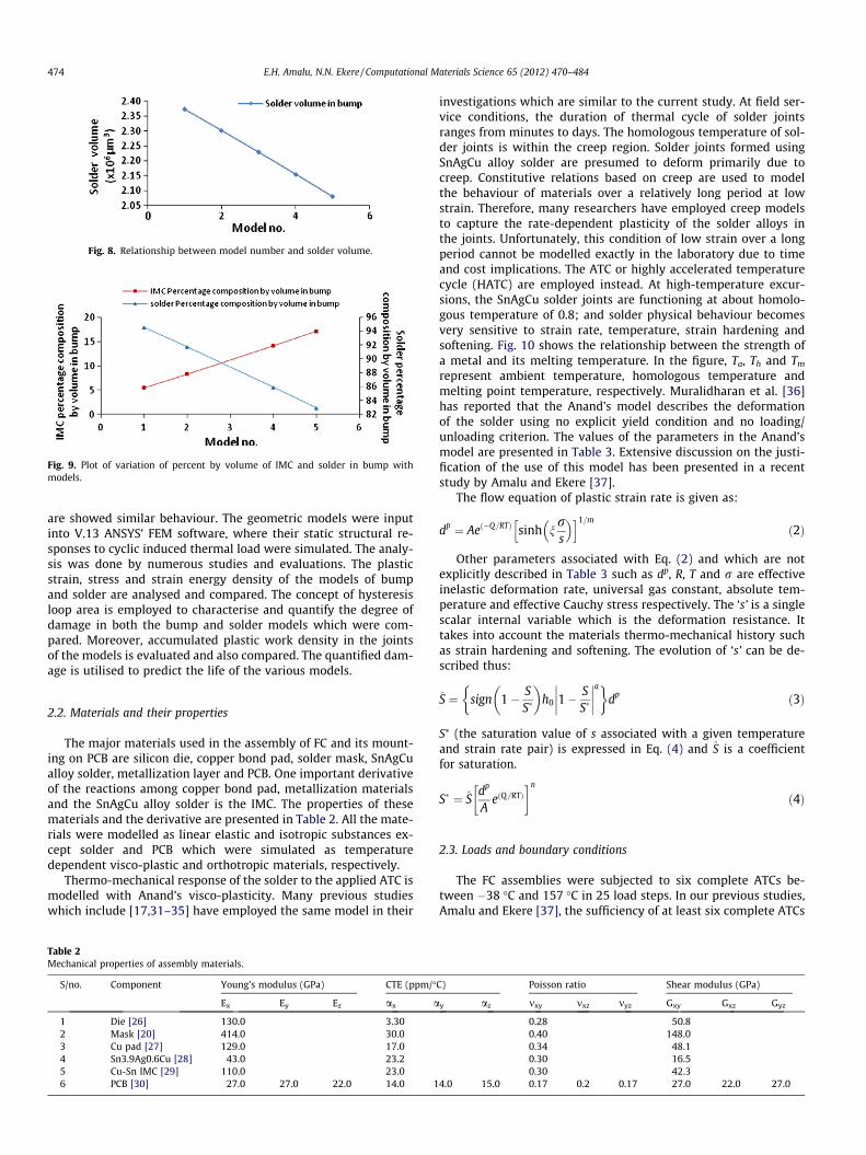
Fig. 8. Relationship between model number and solder volume.
Fig. 9. Plot of variation of percent by volume of IMC and solder in bump withmodels.
474 E.H. Amalu, N.N. Ekere / Computational Materials Science 65 (2012) 470–484
are showed similar behaviour. The geometric models were inputinto V.13 ANSYS’ FEM software, where their static structural re-sponses to cyclic induced thermal load were simulated. The analy-sis was done by numerous studies and evaluations. The plasticstrain, stress and strain energy density of the models of bumpand solder are analysed and compared. The concept of hysteresisloop area is employed to characterise and quantify the degree ofdamage in both the bump and solder models which were com-pared. Moreover, accumulated plastic work density in the jointsof the models is evaluated and also compared. The quantified dam-age is utilised to predict the life of the various models.
2.2. Materials and their properties
The major materials used in the assembly of FC and its mount-ing on PCB are silicon die, copper bond pad, solder mask, SnAgCualloy solder, metallization layer and PCB. One important derivativeof the reactions among copper bond pad, metallization materialsand the SnAgCu alloy solder is the IMC. The properties of thesematerials and the derivative are presented in Table 2. All the mate-rials were modelled as linear elastic and isotropic substances ex-cept solder and PCB which were simulated as temperaturedependent visco-plastic and orthotropic materials, respectively.
Thermo-mechanical response of the solder to the applied ATC ismodelled with Anand’s visco-plasticity. Many previous studieswhich include [17,31–35] have employed the same model in their
Table 2Mechanical properties of assembly materials.
S/no. Component Young’s modulus (GPa) CTE (ppm/�
Ex Ey Ez ax a
1 Die [26] 130.0 3.302 Mask [20] 414.0 30.03 Cu pad [27] 129.0 17.04 Sn3.9Ag0.6Cu [28] 43.0 23.25 Cu-Sn IMC [29] 110.0 23.06 PCB [30] 27.0 27.0 22.0 14.0 1
investigations which are similar to the current study. At field ser-vice conditions, the duration of thermal cycle of solder jointsranges from minutes to days. The homologous temperature of sol-der joints is within the creep region. Solder joints formed usingSnAgCu alloy solder are presumed to deform primarily due tocreep. Constitutive relations based on creep are used to modelthe behaviour of materials over a relatively long period at lowstrain. Therefore, many researchers have employed creep modelsto capture the rate-dependent plasticity of the solder alloys inthe joints. Unfortunately, this condition of low strain over a longperiod cannot be modelled exactly in the laboratory due to timeand cost implications. The ATC or highly accelerated temperaturecycle (HATC) are employed instead. At high-temperature excur-sions, the SnAgCu solder joints are functioning at about homolo-gous temperature of 0.8; and solder physical behaviour becomesvery sensitive to strain rate, temperature, strain hardening andsoftening. Fig. 10 shows the relationship between the strength ofa metal and its melting temperature. In the figure, Ta, Th and Tm
represent ambient temperature, homologous temperature andmelting point temperature, respectively. Muralidharan et al. [36]has reported that the Anand’s model describes the deformationof the solder using no explicit yield condition and no loading/unloading criterion. The values of the parameters in the Anand’smodel are presented in Table 3. Extensive discussion on the justi-fication of the use of this model has been presented in a recentstudy by Amalu and Ekere [37].
The flow equation of plastic strain rate is given as:
dp ¼ Aeð�Q=RTÞ sinh nrs
� �h i1=mð2Þ
Other parameters associated with Eq. (2) and which are notexplicitly described in Table 3 such as dp, R, T and r are effectiveinelastic deformation rate, universal gas constant, absolute tem-perature and effective Cauchy stress respectively. The ‘s’ is a singlescalar internal variable which is the deformation resistance. Ittakes into account the materials thermo-mechanical history suchas strain hardening and softening. The evolution of ‘s’ can be de-scribed thus:
_S ¼ sign 1� SS�
� �h0 1� S
S�
��������a� �
dp ð3Þ
S⁄ (the saturation value of s associated with a given temperatureand strain rate pair) is expressed in Eq. (4) and S is a coefficientfor saturation.
S� ¼ Sdp
AeðQ=RTÞ
n
ð4Þ
2.3. Loads and boundary conditions
The FC assemblies were subjected to six complete ATCs be-tween �38 �C and 157 �C in 25 load steps. In our previous studies,Amalu and Ekere [37], the sufficiency of at least six complete ATCs
C) Poisson ratio Shear modulus (GPa)
y az mxy mxz myz Gxy Gxz Gyz
0.28 50.80.40 148.00.34 48.10.30 16.50.30 42.3
4.0 15.0 0.17 0.2 0.17 27.0 22.0 27.0
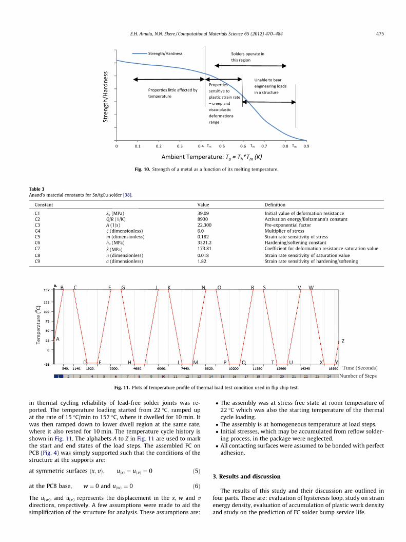
Fig. 10. Strength of a metal as a function of its melting temperature.
Table 3Anand’s material constants for SnAgCu solder [38].
Constant Value Definition
C1 So (MPa) 39.09 Initial value of deformation resistanceC2 Q/R (1/K) 8930 Activation energy/Boltzmann’s constantC3 A (1/s) 22,300 Pre-exponential factorC4 n (dimensionless) 6.0 Multiplier of stressC5 m (dimensionless) 0.182 Strain rate sensitivity of stressC6 ho (MPa) 3321.2 Hardening/softening constantC7 S (MPa) 173.81 Coefficient for deformation resistance saturation value
C8 n (dimensionless) 0.018 Strain rate sensitivity of saturation valueC9 a (dimensionless) 1.82 Strain rate sensitivity of hardening/softening
Fig. 11. Plots of temperature profile of thermal load test condition used in flip chip test.
E.H. Amalu, N.N. Ekere / Computational Materials Science 65 (2012) 470–484 475
in thermal cycling reliability of lead-free solder joints was re-ported. The temperature loading started from 22 �C, ramped upat the rate of 15 �C/min to 157 �C, where it dwelled for 10 min. Itwas then ramped down to lower dwell region at the same rate,where it also rested for 10 min. The temperature cycle history isshown in Fig. 11. The alphabets A to Z in Fig. 11 are used to markthe start and end states of the load steps. The assembled FC onPCB (Fig. 4) was simply supported such that the conditions of thestructure at the supports are:
at symmetric surfaces ðx;vÞ; uðxÞ ¼ uðvÞ ¼ 0 ð5Þ
at the PCB base; w ¼ 0 and uðwÞ ¼ 0 ð6Þ
The u(w), and u(v) represents the displacement in the x, w and vdirections, respectively. A few assumptions were made to aid thesimplification of the structure for analysis. These assumptions are:
� The assembly was at stress free state at room temperature of22 �C which was also the starting temperature of the thermalcycle loading.� The assembly is at homogeneous temperature at load steps.� Initial stresses, which may be accumulated from reflow solder-
ing process, in the package were neglected.� All contacting surfaces were assumed to be bonded with perfect
adhesion.
3. Results and discussion
The results of this study and their discussion are outlined infour parts. These are: evaluation of hysteresis loop, study on strainenergy density, evaluation of accumulation of plastic work densityand study on the prediction of FC solder bump service life.
476 E.H. Amalu, N.N. Ekere / Computational Materials Science 65 (2012) 470–484
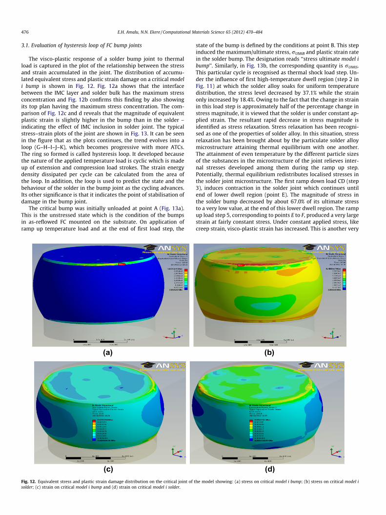
3.1. Evaluation of hysteresis loop of FC bump joints
The visco-plastic response of a solder bump joint to thermalload is captured in the plot of the relationship between the stressand strain accumulated in the joint. The distribution of accumu-lated equivalent stress and plastic strain damage on a critical modeli bump is shown in Fig. 12. Fig. 12a shows that the interfacebetween the IMC layer and solder bulk has the maximum stressconcentration and Fig. 12b confirms this finding by also showingits top plan having the maximum stress concentration. The com-parison of Fig. 12c and d reveals that the magnitude of equivalentplastic strain is slightly higher in the bump than in the solder –indicating the effect of IMC inclusion in solder joint. The typicalstress–strain plots of the joint are shown in Fig. 13. It can be seenin the figure that as the plots continues, the trend evolves into aloop (G–H–I–J–K), which becomes progressive with more ATCs.The ring so formed is called hysteresis loop. It developed becausethe nature of the applied temperature load is cyclic which is madeup of extension and compression load strokes. The strain energydensity dissipated per cycle can be calculated from the area ofthe loop. In addition, the loop is used to predict the state and thebehaviour of the solder in the bump joint as the cycling advances.Its other significance is that it indicates the point of stabilisation ofdamage in the bump joint.
The critical bump was initially unloaded at point A (Fig. 13a).This is the unstressed state which is the condition of the bumpsin as-reflowed FC mounted on the substrate. On application oframp up temperature load and at the end of first load step, the
Fig. 12. Equivalent stress and plastic strain damage distribution on the critical joint of tsolder; (c) strain on critical model i bump and (d) strain on critical model i solder.
state of the bump is defined by the conditions at point B. This stepinduced the maximum/ultimate stress, rUMiB and plastic strain ratein the solder bump. The designation reads ‘‘stress ultimate model ibump’’. Similarly, in Fig. 13b, the corresponding quantity is rUMiS.This particular cycle is recognised as thermal shock load step. Un-der the influence of first high-temperature dwell region (step 2 inFig. 11) at which the solder alloy soaks for uniform temperaturedistribution, the stress level decreased by 37.1% while the strainonly increased by 18.4%. Owing to the fact that the change in strainin this load step is approximately half of the percentage change instress magnitude, it is viewed that the solder is under constant ap-plied strain. The resultant rapid decrease in stress magnitude isidentified as stress relaxation. Stress relaxation has been recogni-sed as one of the properties of solder alloy. In this situation, stressrelaxation has been brought about by the particulate solder alloymicrostructure attaining thermal equilibrium with one another.The attainment of even temperature by the different particle sizesof the substances in the microstructure of the joint relieves inter-nal stresses developed among them during the ramp up step.Potentially, thermal equilibrium redistributes localised stresses inthe solder joint microstructure. The first ramp down load CD (step3), induces contraction in the solder joint which continues untilend of lower dwell region (point E). The magnitude of stress inthe solder bump decreased by about 67.0% of its ultimate stressto a very low value, at the end of this lower dwell region. The rampup load step 5, corresponding to points E to F, produced a very largestrain at fairly constant stress. Under constant applied stress, likecreep strain, visco-plastic strain has increased. This is another very
he model showing: (a) stress on critical model i bump; (b) stress on critical model i
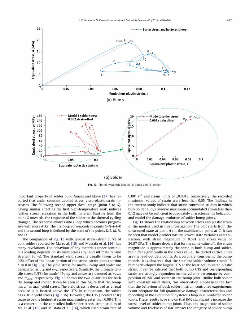
Fig. 13. Plot of hysteresis loop of (a) bump and (b) solder.
E.H. Amalu, N.N. Ekere / Computational Materials Science 65 (2012) 470–484 477
important property of solder bulk. Amalu and Ekere [37] has re-ported that under constant applied stress, visco-plastic strain in-creases. The following second upper dwell stage (point F to G),having similar effect as the first high-temperature soak, inducesfurther stress relaxation in the bulk material. Starting from thepoint G onwards, the response of the solder to the thermal cyclingchanged. The response evolves into a loop which becomes progres-sive with more ATCs. The first loop corresponds to points G–H–I–J–Kand the second loop is defined by the state of the points K, L, M, N,and O.
The comparison of Fig. 13 with typical stress–strain curve ofbulk solder reported by Ma et al. [15] and Mustafa et al. [16] hasmany revelations. The behaviour of any materials under continu-ous loading depends on its yield stress (rY) and ultimate tensilestrength (rUTS). The standard yield stress is usually taken to be0.2% offset of the linear portion of the stress–strain plots (portionA to B in Fig. 13). The yield stress for model i bump and solder aredesignated as rYB and rYS, respectively. Similarly, the ultimate ten-sile stress (UTS) for model i bump and solder are denoted as rUMiB
and rUMiS, respectively. Fig. 13 shows the two quantities for boththe bump and solder. It can be seen in this figure that the bumphas a ‘‘virtual’’ yield stress. The yield stress is described as virtualbecause it is located above the UTS. In comparison, the solderhas a true yield stress (Fig. 13b). However, the UTS (located at B0)cease to be the highest at strain magnitude greater than 0.084. Thisis a concern. In the controlled bulk solder stress–strain studies ofMa et al. [15] and Mustafa et al. [16], which used strain rate of
0.001 s�1 and strain limits of ±0.0018, respectively, the recordedmaximum values of strain were less than 0.05. The findings inthe current study indicate that strain controlled studies in whichbulk solder alloys observe maximum accumulated strain less than0.12 may not be sufficient to adequately characterise the behaviourand model the damage evolution of solder bump joints.
Fig. 14 shows the relationship between stress and plastic strainin the models used in this investigation. The plot starts from theunstressed state at point A till the stabilization point at G. It canbe seen that model 2 solder has the lowest state variables at stabi-lisation, with strain magnitude of 0.091 and stress value of26.87 GPa. The figure depicts that for the same value of i, the strainmagnitude is approximately the same in both bump and solder,but differ significantly in the stress value. The dotted vertical linesare the read out data points. As a corollary, considering the bumpmodels, it is observed that the smallest solder volume (model 5bump) developed the largest UTS at the least accumulated plasticstrain. It can be inferred that both bump UTS and correspondingstrain are strongly dependent on the volume percentage by com-position of IMC and solder in the bump joint. Unlike bulk solderwith constant yield stress, this observation emphasises the factthat the behaviour of buck solder in strain controlled experimentsis not adequate for full quantitative damage characterisation andmodelling of the evolution of hysteresis loop in FC lead-free solderjoints. These results have shown that IMC significantly increase thestress level of solder bump joints. Thus, the magnitude of soldervolume and thickness of IMC impact the integrity of solder bump
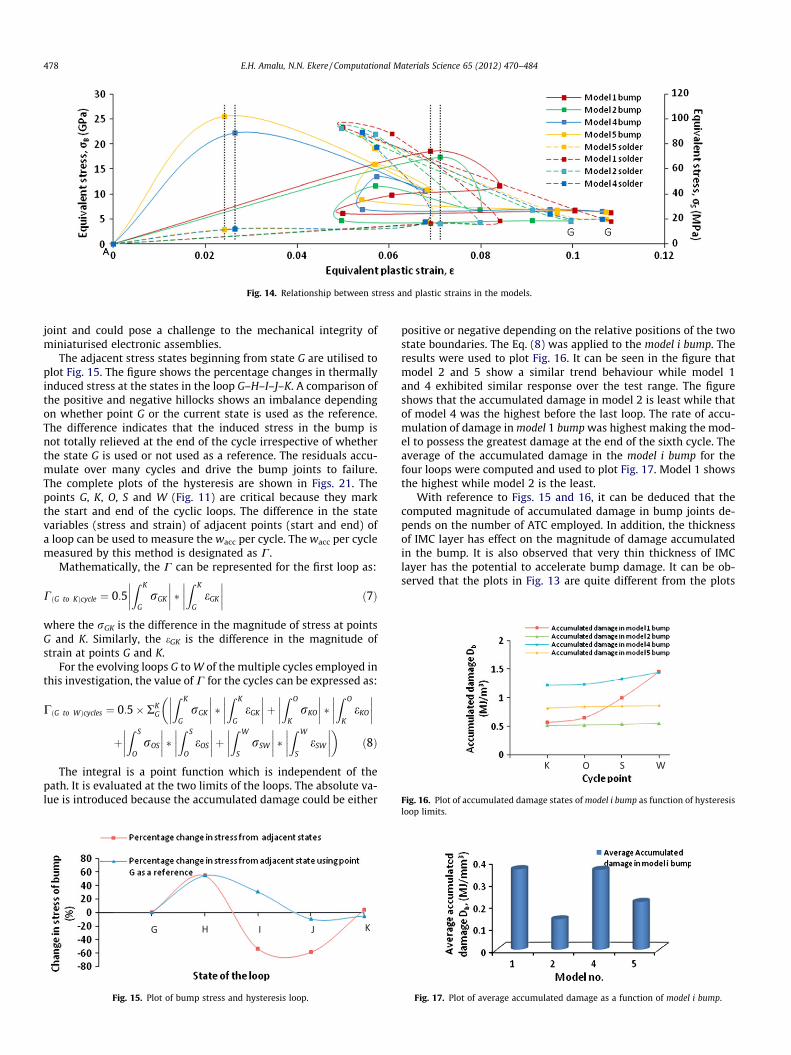
Fig. 14. Relationship between stress and plastic strains in the models.
Fig. 16. Plot of accumulated damage states of model i bump as function of hysteresis
478 E.H. Amalu, N.N. Ekere / Computational Materials Science 65 (2012) 470–484
joint and could pose a challenge to the mechanical integrity ofminiaturised electronic assemblies.
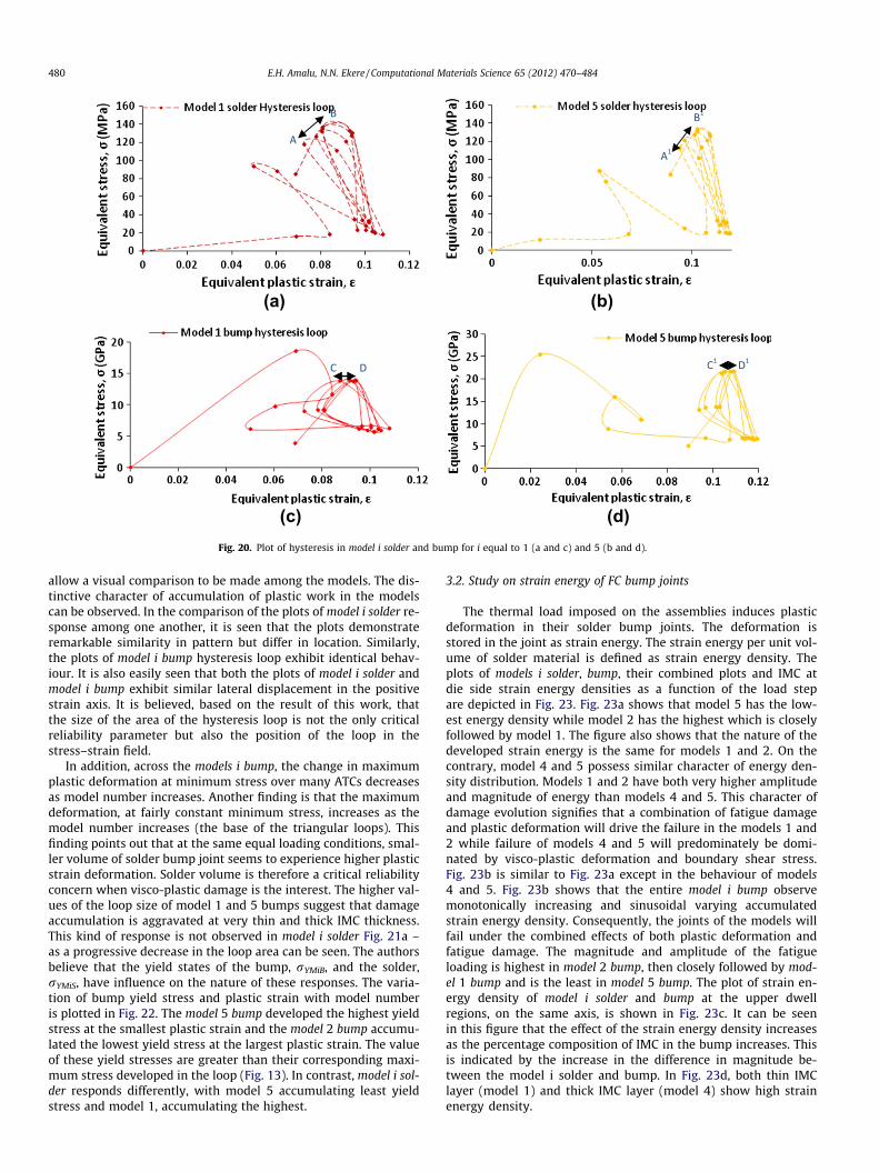
The adjacent stress states beginning from state G are utilised toplot Fig. 15. The figure shows the percentage changes in thermallyinduced stress at the states in the loop G–H–I–J–K. A comparison ofthe positive and negative hillocks shows an imbalance dependingon whether point G or the current state is used as the reference.The difference indicates that the induced stress in the bump isnot totally relieved at the end of the cycle irrespective of whetherthe state G is used or not used as a reference. The residuals accu-mulate over many cycles and drive the bump joints to failure.The complete plots of the hysteresis are shown in Figs. 21. Thepoints G, K, O, S and W (Fig. 11) are critical because they markthe start and end of the cyclic loops. The difference in the statevariables (stress and strain) of adjacent points (start and end) ofa loop can be used to measure the wacc per cycle. The wacc per cyclemeasured by this method is designated as C.
Mathematically, the C can be represented for the first loop as:
CðG to KÞcycle ¼ 0:5Z K
GrGK
�������� �
Z K
GeGK
�������� ð7Þ
where the rGK is the difference in the magnitude of stress at pointsG and K. Similarly, the eGK is the difference in the magnitude ofstrain at points G and K.
For the evolving loops G to W of the multiple cycles employed inthis investigation, the value of C for the cycles can be expressed as:
CðG to WÞcycles ¼ 0:5� RKG
Z K
GrGK
�������� �
Z K
GeGK
��������þ
Z O
KrKO
�������� �
Z O
KeKO
��������
�
þZ S
OrOS
�������� �
Z S
OeOS
��������þ
Z W
SrSW
�������� �
Z W
SeSW
���������
ð8Þ
The integral is a point function which is independent of thepath. It is evaluated at the two limits of the loops. The absolute va-lue is introduced because the accumulated damage could be either
Fig. 15. Plot of bump stress and hysteresis loop.
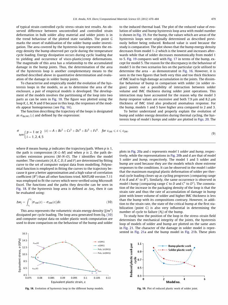
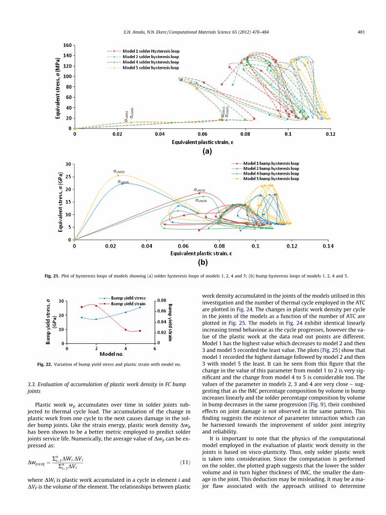
positive or negative depending on the relative positions of the twostate boundaries. The Eq. (8) was applied to the model i bump. Theresults were used to plot Fig. 16. It can be seen in the figure thatmodel 2 and 5 show a similar trend behaviour while model 1and 4 exhibited similar response over the test range. The figureshows that the accumulated damage in model 2 is least while thatof model 4 was the highest before the last loop. The rate of accu-mulation of damage in model 1 bump was highest making the mod-el to possess the greatest damage at the end of the sixth cycle. Theaverage of the accumulated damage in the model i bump for thefour loops were computed and used to plot Fig. 17. Model 1 showsthe highest while model 2 is the least.
With reference to Figs. 15 and 16, it can be deduced that thecomputed magnitude of accumulated damage in bump joints de-pends on the number of ATC employed. In addition, the thicknessof IMC layer has effect on the magnitude of damage accumulatedin the bump. It is also observed that very thin thickness of IMClayer has the potential to accelerate bump damage. It can be ob-served that the plots in Fig. 13 are quite different from the plots
loop limits.
Fig. 17. Plot of average accumulated damage as a function of model i bump.
E.H. Amalu, N.N. Ekere / Computational Materials Science 65 (2012) 470–484 479
of typical strain controlled cyclic stress–strain test results. An ob-served difference between uncontrolled and controlled straindeformation in bulk solder alloy material and solder joints is inthe trend behaviour of the plotted state variables. The point Gmarks the onset of stabilisation of the solder bump under investi-gation. The area covered by the hysteresis loop represents the en-ergy density the bump observed per cycle during the temperaturecycle loading. Energy dissipation occurs during cyclic loading dueto yielding and occurrence of visco-plastic/creep deformations.The magnitude of this area has a relationship to the accumulateddamage in the bump joints. Thus, the determination of the areaof the hysteresis loop is another complementary means to themethod described above in quantitative determination and evalu-ation of the damage in solder bump joints.
To characterise and empirically model the evolution of the hys-teresis loops in the models, so as to determine the area of theenclosure, a pair of empirical models is developed. The develop-ment of the models involves the partitioning of the loop into twoparts as can be seen in Fig. 18. The figure was plotted using theloop K, L, M, N and O because in this loop, the responses of the mod-els appear homogeneous (see Fig. 16).
The function describing the trajectory of the loops is designatedas rBp(Mi) (e) and defined by the expression:
rBpMi
p ¼ 1 or 2i ¼ 1;2;4;5
� ðeÞ ¼ Aþ Be2 þ Ce3 þ De4 þ Ee5 þ Fe6: for e1Mi 6 e 6 e2Mi:ð9Þ
where B means bump, p indicates the trajectory/path. When p is 1,the path is compression (K–L–M) and when p is 2, the path de-scribes extension process (M–N–O). The i identifies the modelnumber. The constants (A, B, C, D, E and F) are determined by fittingcurve to the set of computer output data from modelling. Polyno-mial function is employed in fitting the curves to the trajectory be-cause it gave a better approximation and a high value of correlationcoefficient (R2) than all other functions tried. MATLAB version 7.11was employed to fit the curves which were verified using MicrosoftExcel. The functions and the paths they describe can be seen inFig. 18. If the hysteresis loop area is defined as Dwj, then it canbe evaluated using:
Dwj ¼Z e2
e1
½r1MiðeÞ � r2MiðeÞ�de ð10Þ
This area represents the volumetric strain energy density (J/m3)dissipated per cycle loading. The loop area generated from Eq. (10)and computer output data on solder plastic work computation areused to draw comparison on the behaviour of the bump and solder
Fig. 18. Evolution of hysteresis loop in the different bump models.
to the induced thermal load. The plot of the reduced value of evo-lution of solder and bump hysteresis loop area with model numberis shown in Fig. 19. For the bump, the values which are areas of thehysteresis loops were originally determined as described previ-ously before being reduced. Reduced value is used because thestudy is comparative. The plot shows that the bump energy densitydecreases from model 1–2 which is the lowest and increases after-wards while that of solder decreases monotonically from model 1to 5. Fig. 19 compares well with Fig. 17 in terms of the bump, ex-cept for model 5. The reason for the discrepancy in the behaviour ofmodel 5 in the two scenarios lies on the particular cycle utilised todetermine the area – as demonstrated in Fig. 16. However, it isseen in the two figures that both very thin and too thick thicknessof IMC lead to high damage accumulation in the joints. The dissim-ilar behaviour of bump in comparison with solder (in solder re-gion) points out a possibility of interaction between soldervolume and IMC thickness during solder joint operations. Thisinteraction may have accounted for the reason why the model 3bump response values are excessive and both 7.9 lm and 8.2 lmthickness of IMC tried also produced anomalous response. Forthe bump, models 1 and 5 have higher area compared to 2 and 3.
To better understand and properly explain the evolution ofbump and solder energy densities during thermal cycling, the hys-teresis loop of model i bumps and solder are plotted in Figs. 20. The
Fig. 19. Plot of reduced plastic work of solder joint.
plots in Fig. 20a and c represents model 1 solder and bump, respec-tively, while the representations in Fig. 20b and d are that of model5 solder and bump, respectively. The model 1 and 5 solder andbump are used because they are the models which show extremeresponses to the conditions. It can be observed in the model i solderthat the maximum marginal plastic deformation of solder per ther-mal cycle loading closes up as cycling progresses (comparing rangeA to B and A1 to B1). Similarly, the same occurrence is observed inmodel i bump (comparing range C to D and C1 to D1). The connota-tion of the increase in the packaging density of the loop is that thestrain rate and thus the rate of accumulation of damage in bumpjoint with lower volume of solder and higher IMC thickness is lessthan the bump with its compositions contrary. However, in addi-tion to the strain rate, the state of the critical bump at the first sta-bilization (point G) is also very influential in determining thenumber of cycle to failure (Nf) of the bump.
To study how the position of the loop in the stress–strain fielddetermines the mechanical integrity of the joints, the hysteresisloop of models of solder and bump are plotted on the same axesin Fig. 21. The character of the damage in solder model is repre-sented in Fig. 21a and the bump model in Fig. 21b. These plots
(a) (b)
(c) (d)Fig. 20. Plot of hysteresis in model i solder and bump for i equal to 1 (a and c) and 5 (b and d).
480 E.H. Amalu, N.N. Ekere / Computational Materials Science 65 (2012) 470–484
allow a visual comparison to be made among the models. The dis-tinctive character of accumulation of plastic work in the modelscan be observed. In the comparison of the plots of model i solder re-sponse among one another, it is seen that the plots demonstrateremarkable similarity in pattern but differ in location. Similarly,the plots of model i bump hysteresis loop exhibit identical behav-iour. It is also easily seen that both the plots of model i solder andmodel i bump exhibit similar lateral displacement in the positivestrain axis. It is believed, based on the result of this work, thatthe size of the area of the hysteresis loop is not the only criticalreliability parameter but also the position of the loop in thestress–strain field.
In addition, across the models i bump, the change in maximumplastic deformation at minimum stress over many ATCs decreasesas model number increases. Another finding is that the maximumdeformation, at fairly constant minimum stress, increases as themodel number increases (the base of the triangular loops). Thisfinding points out that at the same equal loading conditions, smal-ler volume of solder bump joint seems to experience higher plasticstrain deformation. Solder volume is therefore a critical reliabilityconcern when visco-plastic damage is the interest. The higher val-ues of the loop size of model 1 and 5 bumps suggest that damageaccumulation is aggravated at very thin and thick IMC thickness.This kind of response is not observed in model i solder Fig. 21a –as a progressive decrease in the loop area can be seen. The authorsbelieve that the yield states of the bump, rYMiB, and the solder,rYMiS, have influence on the nature of these responses. The varia-tion of bump yield stress and plastic strain with model numberis plotted in Fig. 22. The model 5 bump developed the highest yieldstress at the smallest plastic strain and the model 2 bump accumu-lated the lowest yield stress at the largest plastic strain. The valueof these yield stresses are greater than their corresponding maxi-mum stress developed in the loop (Fig. 13). In contrast, model i sol-der responds differently, with model 5 accumulating least yieldstress and model 1, accumulating the highest.
3.2. Study on strain energy of FC bump joints
The thermal load imposed on the assemblies induces plasticdeformation in their solder bump joints. The deformation isstored in the joint as strain energy. The strain energy per unit vol-ume of solder material is defined as strain energy density. Theplots of models i solder, bump, their combined plots and IMC atdie side strain energy densities as a function of the load stepare depicted in Fig. 23. Fig. 23a shows that model 5 has the low-est energy density while model 2 has the highest which is closelyfollowed by model 1. The figure also shows that the nature of thedeveloped strain energy is the same for models 1 and 2. On thecontrary, model 4 and 5 possess similar character of energy den-sity distribution. Models 1 and 2 have both very higher amplitudeand magnitude of energy than models 4 and 5. This character ofdamage evolution signifies that a combination of fatigue damageand plastic deformation will drive the failure in the models 1 and2 while failure of models 4 and 5 will predominately be domi-nated by visco-plastic deformation and boundary shear stress.Fig. 23b is similar to Fig. 23a except in the behaviour of models4 and 5. Fig. 23b shows that the entire model i bump observemonotonically increasing and sinusoidal varying accumulatedstrain energy density. Consequently, the joints of the models willfail under the combined effects of both plastic deformation andfatigue damage. The magnitude and amplitude of the fatigueloading is highest in model 2 bump, then closely followed by mod-el 1 bump and is the least in model 5 bump. The plot of strain en-ergy density of model i solder and bump at the upper dwellregions, on the same axis, is shown in Fig. 23c. It can be seenin this figure that the effect of the strain energy density increasesas the percentage composition of IMC in the bump increases. Thisis indicated by the increase in the difference in magnitude be-tween the model i solder and bump. In Fig. 23d, both thin IMClayer (model 1) and thick IMC layer (model 4) show high strainenergy density.
(a)
(b)Fig. 21. Plot of hysteresis loops of models showing (a) solder hysteresis loops of models 1, 2, 4 and 5; (b) bump hysteresis loops of models 1, 2, 4 and 5.
Fig. 22. Variation of bump yield stress and plastic strain with model no.
E.H. Amalu, N.N. Ekere / Computational Materials Science 65 (2012) 470–484 481
3.3. Evaluation of accumulation of plastic work density in FC bumpjoints
Plastic work wp accumulates over time in solder joints sub-jected to thermal cycle load. The accumulation of the change inplastic work from one cycle to the next causes damage in the sol-der bump joints. Like the strain energy, plastic work density Dwp
has been shown to be a better metric employed to predict solderjoints service life. Numerically, the average value of Dwp can be ex-pressed as:
Dwp;avg ¼Rn
i¼1DWi:DVi
Rni¼1DVi
ð11Þ
where DWi is plastic work accumulated in a cycle in element i andDVP is the volume of the element. The relationships between plastic
work density accumulated in the joints of the models utilised in thisinvestigation and the number of thermal cycle employed in the ATCare plotted in Fig. 24. The changes in plastic work density per cyclein the joints of the models as a function of the number of ATC areplotted in Fig. 25. The models in Fig. 24 exhibit identical linearlyincreasing trend behaviour as the cycle progresses, however the va-lue of the plastic work at the data read out points are different.Model 1 has the highest value which decreases to model 2 and then3 and model 5 recorded the least value. The plots (Fig. 25) show thatmodel 1 recorded the highest damage followed by model 2 and then3 with model 5 the least. It can be seen from this figure that thechange in the value of this parameter from model 1 to 2 is very sig-nificant and the change from model 4 to 5 is considerable too. Thevalues of the parameter in models 2, 3 and 4 are very close – sug-gesting that as the IMC percentage composition by volume in bumpincreases linearly and the solder percentage composition by volumein bump decreases in the same progression (Fig. 9), their combinedeffects on joint damage is not observed in the same pattern. Thisfinding suggests the existence of parameter interaction which canbe harnessed towards the improvement of solder joint integrityand reliability.
It is important to note that the physics of the computationalmodel employed in the evaluation of plastic work density in thejoints is based on visco-plasticity. Thus, only solder plastic workis taken into consideration. Since the computation is performedon the solder, the plotted graph suggests that the lower the soldervolume and in turn higher thickness of IMC, the smaller the dam-age in the joint. This deduction may be misleading. It may be a ma-jor flaw associated with the approach utilised to determine
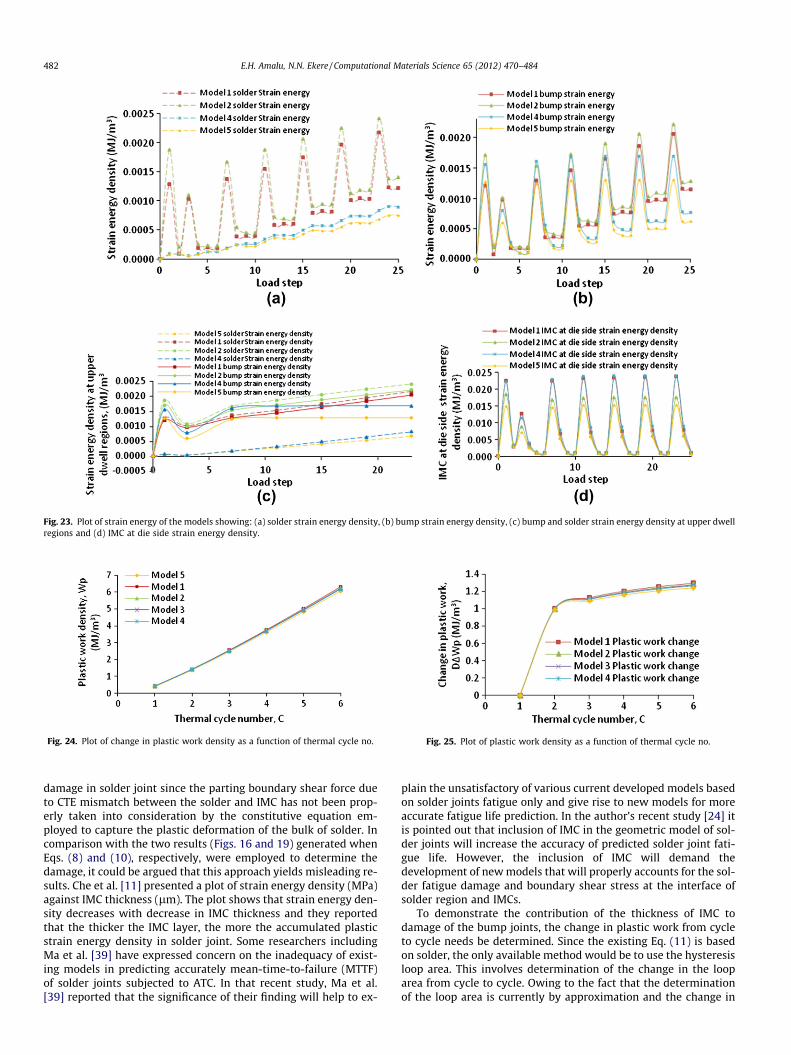
Fig. 23. Plot of strain energy of the models showing: (a) solder strain energy density, (b) bump strain energy density, (c) bump and solder strain energy density at upper dwellregions and (d) IMC at die side strain energy density.
Fig. 24. Plot of change in plastic work density as a function of thermal cycle no. Fig. 25. Plot of plastic work density as a function of thermal cycle no.
482 E.H. Amalu, N.N. Ekere / Computational Materials Science 65 (2012) 470–484
damage in solder joint since the parting boundary shear force dueto CTE mismatch between the solder and IMC has not been prop-erly taken into consideration by the constitutive equation em-ployed to capture the plastic deformation of the bulk of solder. Incomparison with the two results (Figs. 16 and 19) generated whenEqs. (8) and (10), respectively, were employed to determine thedamage, it could be argued that this approach yields misleading re-sults. Che et al. [11] presented a plot of strain energy density (MPa)against IMC thickness (lm). The plot shows that strain energy den-sity decreases with decrease in IMC thickness and they reportedthat the thicker the IMC layer, the more the accumulated plasticstrain energy density in solder joint. Some researchers includingMa et al. [39] have expressed concern on the inadequacy of exist-ing models in predicting accurately mean-time-to-failure (MTTF)of solder joints subjected to ATC. In that recent study, Ma et al.[39] reported that the significance of their finding will help to ex-
plain the unsatisfactory of various current developed models basedon solder joints fatigue only and give rise to new models for moreaccurate fatigue life prediction. In the author’s recent study [24] itis pointed out that inclusion of IMC in the geometric model of sol-der joints will increase the accuracy of predicted solder joint fati-gue life. However, the inclusion of IMC will demand thedevelopment of new models that will properly accounts for the sol-der fatigue damage and boundary shear stress at the interface ofsolder region and IMCs.
To demonstrate the contribution of the thickness of IMC todamage of the bump joints, the change in plastic work from cycleto cycle needs be determined. Since the existing Eq. (11) is basedon solder, the only available method would be to use the hysteresisloop area. This involves determination of the change in the looparea from cycle to cycle. Owing to the fact that the determinationof the loop area is currently by approximation and the change in
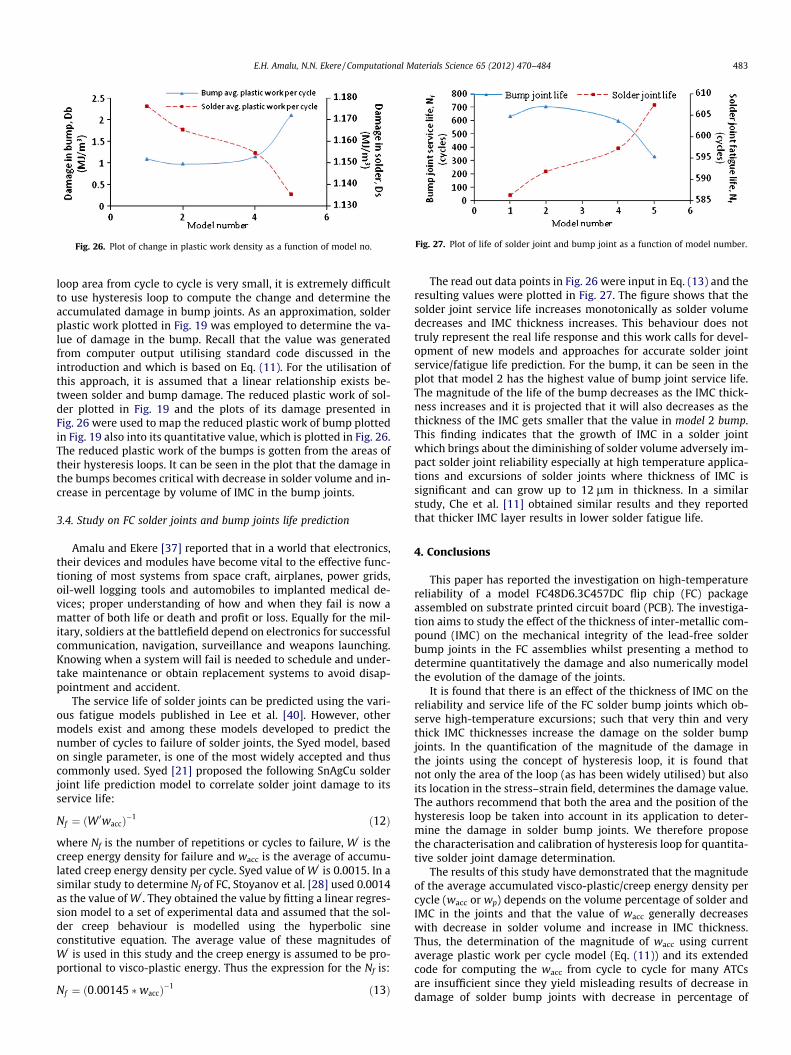
Fig. 26. Plot of change in plastic work density as a function of model no. Fig. 27. Plot of life of solder joint and bump joint as a function of model number.
E.H. Amalu, N.N. Ekere / Computational Materials Science 65 (2012) 470–484 483
loop area from cycle to cycle is very small, it is extremely difficultto use hysteresis loop to compute the change and determine theaccumulated damage in bump joints. As an approximation, solderplastic work plotted in Fig. 19 was employed to determine the va-lue of damage in the bump. Recall that the value was generatedfrom computer output utilising standard code discussed in theintroduction and which is based on Eq. (11). For the utilisation ofthis approach, it is assumed that a linear relationship exists be-tween solder and bump damage. The reduced plastic work of sol-der plotted in Fig. 19 and the plots of its damage presented inFig. 26 were used to map the reduced plastic work of bump plottedin Fig. 19 also into its quantitative value, which is plotted in Fig. 26.The reduced plastic work of the bumps is gotten from the areas oftheir hysteresis loops. It can be seen in the plot that the damage inthe bumps becomes critical with decrease in solder volume and in-crease in percentage by volume of IMC in the bump joints.
3.4. Study on FC solder joints and bump joints life prediction
Amalu and Ekere [37] reported that in a world that electronics,their devices and modules have become vital to the effective func-tioning of most systems from space craft, airplanes, power grids,oil-well logging tools and automobiles to implanted medical de-vices; proper understanding of how and when they fail is now amatter of both life or death and profit or loss. Equally for the mil-itary, soldiers at the battlefield depend on electronics for successfulcommunication, navigation, surveillance and weapons launching.Knowing when a system will fail is needed to schedule and under-take maintenance or obtain replacement systems to avoid disap-pointment and accident.
The service life of solder joints can be predicted using the vari-ous fatigue models published in Lee et al. [40]. However, othermodels exist and among these models developed to predict thenumber of cycles to failure of solder joints, the Syed model, basedon single parameter, is one of the most widely accepted and thuscommonly used. Syed [21] proposed the following SnAgCu solderjoint life prediction model to correlate solder joint damage to itsservice life:
Nf ¼ ðW 0waccÞ�1 ð12Þ
where Nf is the number of repetitions or cycles to failure, W0
is thecreep energy density for failure and wacc is the average of accumu-lated creep energy density per cycle. Syed value of W
0is 0.0015. In a
similar study to determine Nf of FC, Stoyanov et al. [28] used 0.0014as the value of W
0. They obtained the value by fitting a linear regres-
sion model to a set of experimental data and assumed that the sol-der creep behaviour is modelled using the hyperbolic sineconstitutive equation. The average value of these magnitudes ofW
0is used in this study and the creep energy is assumed to be pro-
portional to visco-plastic energy. Thus the expression for the Nf is:
Nf ¼ ð0:00145 �waccÞ�1 ð13Þ
The read out data points in Fig. 26 were input in Eq. (13) and theresulting values were plotted in Fig. 27. The figure shows that thesolder joint service life increases monotonically as solder volumedecreases and IMC thickness increases. This behaviour does nottruly represent the real life response and this work calls for devel-opment of new models and approaches for accurate solder jointservice/fatigue life prediction. For the bump, it can be seen in theplot that model 2 has the highest value of bump joint service life.The magnitude of the life of the bump decreases as the IMC thick-ness increases and it is projected that it will also decreases as thethickness of the IMC gets smaller that the value in model 2 bump.This finding indicates that the growth of IMC in a solder jointwhich brings about the diminishing of solder volume adversely im-pact solder joint reliability especially at high temperature applica-tions and excursions of solder joints where thickness of IMC issignificant and can grow up to 12 lm in thickness. In a similarstudy, Che et al. [11] obtained similar results and they reportedthat thicker IMC layer results in lower solder fatigue life.
4. Conclusions
This paper has reported the investigation on high-temperaturereliability of a model FC48D6.3C457DC flip chip (FC) packageassembled on substrate printed circuit board (PCB). The investiga-tion aims to study the effect of the thickness of inter-metallic com-pound (IMC) on the mechanical integrity of the lead-free solderbump joints in the FC assemblies whilst presenting a method todetermine quantitatively the damage and also numerically modelthe evolution of the damage of the joints.
It is found that there is an effect of the thickness of IMC on thereliability and service life of the FC solder bump joints which ob-serve high-temperature excursions; such that very thin and verythick IMC thicknesses increase the damage on the solder bumpjoints. In the quantification of the magnitude of the damage inthe joints using the concept of hysteresis loop, it is found thatnot only the area of the loop (as has been widely utilised) but alsoits location in the stress–strain field, determines the damage value.The authors recommend that both the area and the position of thehysteresis loop be taken into account in its application to deter-mine the damage in solder bump joints. We therefore proposethe characterisation and calibration of hysteresis loop for quantita-tive solder joint damage determination.
The results of this study have demonstrated that the magnitudeof the average accumulated visco-plastic/creep energy density percycle (wacc or wp) depends on the volume percentage of solder andIMC in the joints and that the value of wacc generally decreaseswith decrease in solder volume and increase in IMC thickness.Thus, the determination of the magnitude of wacc using currentaverage plastic work per cycle model (Eq. (11)) and its extendedcode for computing the wacc from cycle to cycle for many ATCsare insufficient since they yield misleading results of decrease indamage of solder bump joints with decrease in percentage of
484 E.H. Amalu, N.N. Ekere / Computational Materials Science 65 (2012) 470–484
solder volume and increase in percentage of IMC. This is a reasonwhy existing life prediction models based on wacc have been unsat-isfactory in many of their applications as have been widely re-ported in numerous studies in the literature. Since we haveshown in this investigation that the character of the damage profileof the FC solder bump joints is dependent on the percentage bycomposition of solder and IMC in the bumps, we propose that dam-age of solder bump joints be characterised as a function of the per-centage by volume of solder and IMC in the joints. We also proposethat new damage life prediction models be specific on theseparameters.
Strain controlled study on bulk solder, not up to stain range of0.07–0.12, is not adequate to characterise damage behaviour andmodel damage evolution in FC solder bump joints. The inadequacyof such studies is heightened by the absence of IMC in their testvehicles.
Acknowledgements
The authors acknowledge the funds received from PetroleumTechnology Development Fund (PTDF) Nigeria and the School ofEngineering, University of Greenwich, UK. We also acknowledgethe support of EMERG staff/researchers especially Mrs. SharonWood and Mrs. Nicola Cox. In addition, we would like to thankMr. Galadima Aminu of Petroleum Technology Development Fund,Abuja, Nigeria.
References
[1] W. Peng, E. Monlevade, M.E. Marques, Microelectronics Reliability 47 (12)(2007) 2161–2168.
[2] T. Laurila, T. Mattila, V. Vuorinen, J. Karppinen, J. Li, M. Sippola, J.K. Kivilahti,Microelectronics Reliability 47 (7) (2007) 1135–1144.
[3] P. Arulvanan, Z. Zhong, X. Shi. Microelectronics Reliability 46(2–4) (2006) 432–439.
[4] P. Chauhan, M. Mueller, M. Osterman, M. Pecht, in: Proceedings of ElectronicSystem-Integration Technology Conference (ESTC), 2010, pp. 1–10.
[5] C. Wang, F. Qin, T. An, in: Proceedings of 11th International Conference onElectronic Packaging Technology & High Density Packaging (ICEPT-HDP), 2010,pp. 511–514.
[6] K. Lee, M. Li, Journal of Electronic Materials 32 (8) (2003) 906–912.[7] L. Xu, J.H.L. Pang, K.H.P. Prakash, T.H. Low, IEEE Transactions on Electronics
Packaging Manufacturing 28 (3) (2005) 408–414.[8] C.Y. Liu, C. Chen, A.K. Mal, K.N. Tu, Journal of Applied Physics 85 (1999) 3882.[9] K.S. Kim, S.H. Huh, K. Suganuma, Journal of Alloys and Compounds 352 (1–2)
(2003) 226–236.[10] Y.C. Chan, P.L. Tu, C.W. Tang, K.C. Hung, J.K.L. Lai, IEEE Transactions on
Advanced Packaging 24 (1) (2001) 25–32.[11] F.-X. Che, J.H.L. Pang, L.H. Xu, in: Proceedings of the Tenth Intersociety
Conference on Thermal and Thermomechanical Phenomena in ElectronicsSystems, ITHERM ’06, 2006, pp. 1018–1023.
[12] G.J.S. Chou, in: Proceedings of 8th International Symposium on AdvancedPackaging Materials, 2002, pp. 39–46.
[13] J.H.L. Pang, T.H. Low, B.S. Xiong, X. Luhua, C.C. Neo, Thin Solid Films 462–463(2004) 370–375.
[14] S. Wiese, K.J. Wolter, Microelectronics Reliability 47 (2–3) (2007) 223–232.[15] H. Ma, J.C. Suhling, Y. Zhang, P. Lall, M. J. Bozack, in: Proceedings of Electronic
Components and Technology Conference, vol. 57, 2007, pp. 653-668.[16] M. Mustafa, Z. Cai, J.C. Suhling, P. Lall, in: Proceedings of Electronic
Components and Technology Conference (ECTC), vol. 61, 2011, pp. 927–939.[17] J. Yang, C.I. Ume, in: Proceedings of Electronic Components and Technology
Conference, vol. 58, 2008, pp. 611–622.[18] F.A. Stam, E. Davitt, Microelectronics Reliability 41 (11) (2001) 1815–1822.[19] Y. Qi, H.R. Ghorbani, J.K. Spelt, IEEE Transactions on Advanced Packaging 29 (4)
(2006) 690–700.[20] B.A. Zahn, in: Proceedings of Electronic Components and Technology
Conference, vol. 52, 2002, pp. 1475–1483.[21] A. Syed, in: Proceedings of Electronic Components and Technology Conference,
vol. 54, 2004, pp. 737–746.[22] I. Guven, V. Kradinov, E. Madenci, ASME Journal of Electronic Packaging 126 (3)
(2004) 398–405.[23] X. Li, Z. Wang, Journal of Materials Processing Technology 183 (1) (2007) 6–12.[24] E.H. Amalu, N.N. Ekere, Journal of Materials Processing Technology 212 (2012)
471–483.[25] E. George, D. Das, M. Osterman, M. Pecht, IEEE Transactions on Device and
Materials Reliability 11 (2) (2011) 328–338.[26] Z. Zhang, S. Park, K. Darbha, R.N. Master, in: Proceedings of Electronic
Components and Technology Conference, vol. 60, 2010, pp. 14–19.[27] T.T. Nguyen, D. Lee, J.B. Kwak, S. Park, Microelectronics Reliability 50 (2010)
1000–1006.[28] S. Stoyanov, C. Bailey, M. Desmulliez, Soldering & Surface Mount Technology
21 (1) (2009) 11–24.[29] K. Sakuma, K. Sueoka, S. Kohara, K. Matsumoto, H. Noma, T. Aoki, Y. Oyama, H.
Nishiwaki, P.S. Andry, C.K. Tsang, J.U. Knickerbocker, Y. Orji, ElectronicComponents and Technology Conference (2010) 864–871.
[30] High Performance FR-4 for Multi-Layered PWB Copper Clad Laminates, 17December 2009. Available from: <http://www.mgc.co.jp/eng/products/lm/btprint/lineup/fr4.html>. [Cited 2011 29th March]
[31] E.H. Amalu, N.N. Ekere, R.S. Bhatti, S. Mallik, G. Takyi, A.O.A. Ibhadode, Science& Technology (2010) 1242–1251.
[32] S. Chen, Y. Lin, C. Cheng, Journal of Materials Processing Technology 171(2006) 125–131.
[33] K.J.L. Geisler, M.M. Holahan, in: Proceedings of Electronic Components andTechnology Conference, vol. 60, 2010, pp. 106–113.
[34] C.J. Zhai, Sidharth, R. Blish II, IEEE Transactions on Device and MaterialsReliability (2003) 207–212.
[35] L. Zhang, R. Sitaraman, V. Patwardhan, L. Nguyen, N. Kelkar, ElectronicComponents and Technology Conference (2003) 572–577.
[36] G. Muralidharan, K. Kurumaddali, A.K. Kercher, S.G. Leslie Proc, ElectronicComponents and Technology Conference 60 (2010) 1823–1829.
[37] E.H. Amalu, N.N. Ekere, Microelectronics Reliability (2012). http://dx.doi.org/10.1016/j.microrel.2012.04.004.
[38] M.O. Alam, H. Lu, C. Bailey, Y.C. Chan, Computational Materials Science 45 (2)(2009) 576–583.
[39] H. Ma, M. Ahmad, K.-C. Liu, Electronic Components and TechnologyConference (2010) 1816–1822.
[40] W.W. Lee, L.T. Nguyen, G.S. Selvaduray, Microelectronics Reliability 40 (2)(2000) 231–244.