Embed Size (px)
Citation preview
Current Conduction in Poly(3-Hexylthiophene) and in Poly(3-Hexylthiophene) doped [6,6]-Phenyl C61-Butyric Acid MethylesterComposite Thin Film DevicesZivayi Chiguvarea and Jurgen Parisib
a University of the Witwatersrand, School of Physics (DST/CoESM, MPRI), Private Bag 3, Wits2050, Johannesburg, South Africa
b University of Oldenburg, Energy and Semiconductor Research, 26111, Oldenburg, Germany
Reprint requests to Z. C.; E-mail: [email protected]
Z. Naturforsch. 67a, 589 – 600 (2012) / DOI: 10.5560/ZNA.2012-0062Received March 26, 2012 / revised June 6, 2012 / published online September 12, 2012
Transport properties of poly(3-hexylthiophene) (P3HT), and of its blend with [6,6]-phenyl C61-butyric acid methylester (PCBM), were studied by analysing temperature dependent current–voltagecharacteristics of spin cast thin films sandwiched between aluminium electrodes in a metal–insulator–metal (MIM) configuration. It was found that in Al/P3HT/Al devices, the current is limited by spacecharge that accumulates near the hole injecting electrode due to the poor bulk transport propertiesof P3HT. At low temperatures and high applied electric fields the current density obeys a powerlaw of the form J ∼ V m, characteristic of space charge limited current (SCLC) in the presence ofexponentially distributed traps within the band gap. These traps are filled by charge that is injected byquantum mechanical tunnelling, which is adequately described by the Fowler–Nordheim (FN) theory.By calculating the majority charge carrier mobility in Al/P3HT/Al and Al/P3HT:PCBM/Al devicesfrom the Ohmic, SCLC, and FN tunnelling fits at different temperatures, we have obtained that thecharge carrier mobility in P3HT is two orders smaller than the electron mobility in the P3HT:PCBMblend at room temperature, but comparable at low temperatures. This information is important indetermining the origin of open circuit voltage and short circuit current limit in solar cells that employthis blend as the active layer.
Key words: Polymer Semiconductors; Space Charge Limited Currents; Trap Filling; MIM Devices;Fowler–Nordheim Tunnelling.
PACS numbers: 72.20.Ht; 72.80.Le; 73.40.Rw; 73.40.Sx; 82.35.Cd; 85.30.De
1. Introduction
1.1. Motivation
Organic polymers are interesting materials for thefabrication of electrically conducting devices such aslight emitting diodes [1], solar cells [2 – 4], and thinfilm field effect transistors [5] on flexible substrates.Poly(3-hexylthiophene) (P3HT) has emerged as one ofthe very promising materials and is currently a sub-ject of intense research. Photovoltaic devices employ-ing P3HT:PCBM blends as the active layer with re-producible efficiency as high as 5% at 100 mW/cm2,AM1.5 radiation have been achieved [6, 7]. Certifiedpower conversion efficiency of 8.3% has been reportedfor bulk heterojunction organic solar cells [8], andcommercial manufacture for application in consumerelectronics has started.
The electron collecting electrode in polymer-fullerene heterojunction solar cells is usually alu-minium, which is in contact with both P3HT andPCBM. Open circuit voltages of ∼ 0.6 V and abovehave been achieved in these solar cells, which biasesthe device with electrical fields ∼ 3 ·10−4 V/cm fora 200 nm thick solar cell. Current flow in these devicesis therefore strongly influenced by the photo-generatedvoltage. The understanding of the basic physics under-lying the electrical, thermal, and optical behaviour oforganic polymeric materials [9], and their blends withfullerenes [10], as well as charge injection and col-lection dynamics across interfaces, is essential for theoptimisation of devices fabricated using these materi-als.
In this paper, we intend to contribute towards theunderstanding of charge injection dynamics across
© 2012 Verlag der Zeitschrift fur Naturforschung, Tubingen · http://znaturforsch.com
590 Z. Chiguvare and J. Parisi · Current Conduction in P3HT and in P3HT:PCBM Composite Thin Film Devices
Al/P3HT and Al/PCBM interfaces and charge trans-port in these devices. We investigate the effect of bi-asing thin films of P3HT and P3HT:PCBM blends interms of how charge is injected across the interfacesand transported through the bulk. By reverse analogy,this could assist in the understanding of charge col-lection from solar cells made using these materials.We report on a study of electrical and thermal prop-erties of spin-cast films of P3HT and P3HT:PCBMblends, sandwiched between aluminium electrodes ina MIM configuration. Characteristic hole trap depthswere quantified for each temperature, then used to ob-tain the characteristic trap energy and the total trapdensity in the P3HT films. We describe the com-plete J(V ) curves through a model that incorporatesRichardson–Schottky (RS) thermionic, and FN tun-nelling currents. Ohmic, SCLC, and FN theories wereemployed in obtaining the charge carrier densities
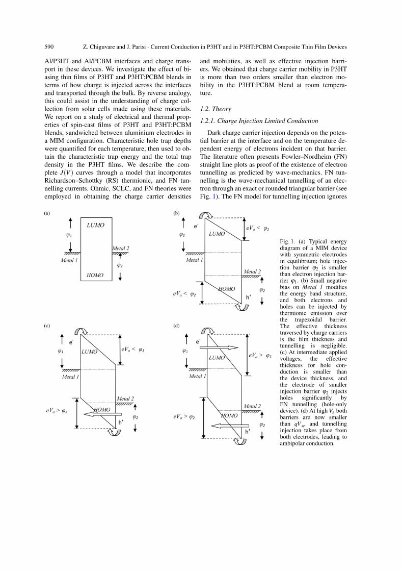
Fig. 1. (a) Typical energydiagram of a MIM devicewith symmetric electrodesin equilibrium; hole injec-tion barrier ϕ2 is smallerthan electron injection bar-rier ϕ1. (b) Small negativebias on Metal 1 modifiesthe energy band structure,and both electrons andholes can be injected bythermionic emission overthe trapezoidal barrier.The effective thicknesstraversed by charge carriersis the film thickness andtunnelling is negligible.(c) At intermediate appliedvoltages, the effectivethickness for hole con-duction is smaller thanthe device thickness, andthe electrode of smallerinjection barrier ϕ2 injectsholes significantly byFN tunnelling (hole-onlydevice). (d) At high Va bothbarriers are now smallerthan qV a, and tunnellinginjection takes place fromboth electrodes, leading toambipolar conduction.
and mobilities, as well as effective injection barri-ers. We obtained that charge carrier mobility in P3HTis more than two orders smaller than electron mo-bility in the P3HT:PCBM blend at room tempera-ture.
1.2. Theory
1.2.1. Charge Injection Limited Conduction
Dark charge carrier injection depends on the poten-tial barrier at the interface and on the temperature de-pendent energy of electrons incident on that barrier.The literature often presents Fowler–Nordheim (FN)straight line plots as proof of the existence of electrontunnelling as predicted by wave-mechanics. FN tun-nelling is the wave-mechanical tunnelling of an elec-tron through an exact or rounded triangular barrier (seeFig. 1). The FN model for tunnelling injection ignores
Z. Chiguvare and J. Parisi · Current Conduction in P3HT and in P3HT:PCBM Composite Thin Film Devices 591
image charge effects and invokes tunnelling of elec-trons from the metal through a triangular barrier intounbound continuum states. It predicts that the currentdensity
J(F) =q3
16π2}ϕF2 exp
[−4(2meff)
12 ·ϕ 3
2
3}qF
](1)
is independent of temperature. Here meff is the effec-tive mass of the carrier inside the dielectric, q the elec-tronic charge, F = Va/d, where Va is the applied elec-tric field, d the film thickness, and ϕ the unmodifiedpotential barrier at the metal contact/polymer inter-face. Barrier lowering due to an applied electric fieldmay become comparable to the barrier height itselfat higher fields, and its neglect in tunnelling consid-erations is problematic as are the tacit assumptionsof a triangular barrier and the existence of a contin-uum of unbound states into which carriers can tun-nel.
The essential assumption of the Richardson–Schottky (RS) model of thermionic emission is thatan electron from the metal can be injected once it hasacquired a thermal energy sufficient to cross the po-tential maximum that results from the superposition ofthe external and the image charge potential (see curvedarrows in Fig. 1). Neither is tunnelling considered norinelastic scattering of the hot carrier before traversingthe potential maximum. The J(F) characteristic is pre-
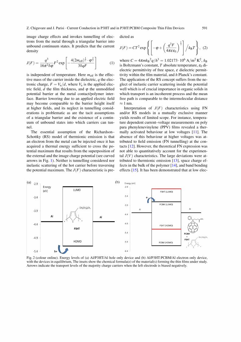
Fig. 2 (colour online). Energy levels of (a) Al/P3HT/Al hole only device and (b) Al/P3HT:PCBM/Al electron only device,with the devices in equilibrium, The insets show the chemical formula(e) of the material(s) forming the thin films under study.Arrows indicate the transport levels of the majority charge carriers when the left electrode is biased negatively.
dicted as
J(F) = CT 2 exp
−ϕ +
(q3F
4πεε0
) 12
/kBT
, (2)
where C = 4πmkB2q/h3 = 1.02173 ·106 A/m2 K2, kB
is Boltzmann’s constant, T absolute temperature, ε0 di-electric permittivity of free space, ε dielectric permit-tivity within the film material, and h Planck’s constant.The application of the RS concept suffers from the ne-glect of inelastic carrier scattering inside the potentialwell which is of crucial importance in organic solids inwhich transport is an incoherent process and the meanfree path is comparable to the intermolecular distance≈ 1 nm.
Interpretation of J(F) characteristics using FNand/or RS models in a mutually exclusive manneryields results of limited scope. For instance, tempera-ture dependent current–voltage measurements on polypara phenylenevinylene (PPV) films revealed a ther-mally activated behaviour at low voltages [11]. Theabsence of this behaviour at higher voltages was at-tributed to field emission (FN tunnelling) at the con-tacts [12]. However, the theoretical FN expression wasnot able to quantitatively account for the experimen-tal J(V ) characteristics. The large deviations were at-tributed to thermionic emission [13], space charge ef-fects in the bulk of the polymer [14], and band bendingeffects [15]. It has been demonstrated that at low elec-

592 Z. Chiguvare and J. Parisi · Current Conduction in P3HT and in P3HT:PCBM Composite Thin Film Devices
tric fields and at room temperature the conduction ofholes in PPV devices is limited by space charge effectsin the bulk of the polymer and not by the charge injec-tion from the contact [16]. At high fields however, thestrong field dependence of the current together with itsdecreased temperature dependence both seem to arguein favour of the tunnelling model [17].
We have shown that the determination of whetherconduction is contact injection limited or bulk lim-ited is dependent upon the balance between the appliedfield and the temperature, where the threshold field forswitch over from RS thermionic emission to FN fieldemission is determined by [18]
F =2√
2mkBT φ32
q}(φ − kBT ), (3)
when the sample is maintained at constant temperature.As T increases, the numerator increases, while the de-nominator decreases, hence F required for tunnellingto dominate the characteristics becomes higher. Whenϕ ≤ kBT , (3) is not defined, i.e. all charges have energyequal to or greater than that required to overcome thebarrier, therefore only thermionic emission will occur,and the definition of quantum mechanical tunnellingis not applicable. In general, for metal/polymer inter-faces it may be assumed that if RS thermionic injectiondominated the injection process, then bulk conductionshould be the limiting factor. If tunnelling is dominantat high F , then the contact is a limiting factor at lowF only. It is possible to realize SCLC independent ofinjection mechanism. We show in this paper that thetwo charge injection mechanisms are not mutually ex-clusive and can occur at the same time within a device.
1.2.2. Charge Transport in the Bulk
Once charge carriers are injected, their transportthrough the polymer layer towards the adjacent elec-trode under the influence of the external electric fieldis determined by the conduction properties of the ma-terial itself. For low bias the number of injected carri-ers is smaller or comparable to the thermally generatedintrinsic charge carriers, and the current–voltage char-acteristics can be described by Ohm’s law:
JOhm = qnµVa
d, (4)
where n is the density of the majority charge car-rier, and µ is the charge carrier mobility. The space
charge limited current (SCLC) model [19, 20] de-scribes charge injection into a low conductivity mate-rial, where the concentration of injected charge mayexceed the intrinsic charge concentration, and spacecharge builds in the sample. Fits of this model pro-vide useful material characteristics such as the trap dis-tribution in the energy band gap, the position of theFermi energy level, and charge carrier mobility. Inves-tigations of low barrier devices have shown that bulkconduction in disordered, and that in undoped, conju-gated polymers is also described well by the hoppingtransport of electrons and holes, taking into accountspace charge effects and traps of different depths [21].
Current density–voltage, J(V ), characteristics ofelectrode/polymer/electrode devices can often be fit-ted excellently by the power law J ∼ V m with m > 2,characteristic of the filling of exponentially distributedtraps [22]. Traps may originate from structural defectsor due to perturbed molecules in the lattice causingcharge of polarisation energy in the perturbed regions,which may also tend to lower the bottom edge of theconduction band or to raise the bottom edge of the va-lence band. Campbell et al. [23] have shown that theSCLC model with field independent mobility, in pres-ence of exponentially distributed traps gives qualita-tively the same results as trap free space charge limitedcurrent (TFSCLC) with a field dependent mobility ofthe Poole–Frenkel type [24 – 26].
The specific functional form of the SCLC J(V )curve depends on the distribution of charge traps in theband gap. For traps that are exponentially distributedwithin the energy band gap, it is
N(E) = Nvb exp
(− E
Et
), (5)
where N(E) is the trap density per unit energy rangeat an energy level E above the valence band edge,and Nvb is the trap density at the valence band edge(Nvb = Ntotal/kBTt); Et is the characteristic constant ofthe distribution, also often expressed as a character-istic temperature Tt, (Et = kBTt), where kB is Boltz-mann’s constant. The exponential distribution of trapsin a hole-only device implies a power law dependenceof J on V given by [19, 20]:
J = q1−lµpNv
(2l +1l−1
) 1l(
ll +1
εε0
Ntotal
)l V l+1
d2l+1 , (6)
where µp is the charge carrier mobility of holes, Nvthe density of states in the valence band, Ntotal the total
Z. Chiguvare and J. Parisi · Current Conduction in P3HT and in P3HT:PCBM Composite Thin Film Devices 593
density of traps; l = Tt/T , T is the measurement tem-perature in K, m = l +1, and J ∼V m is the power lawobtained. In that case, the quasi-Fermi level, which de-pends on the magnitude of stored charge and hence onthe applied voltage, is given by
EF(V ) = kBTt ln
[f (l)
qNtotald2
εε0V
], (7)
where
f (l) =(
2l +1l +1
)− 1l (l +1)2
l (2l +1), (8)
and 0.5 ≤ f (l) ≤ 8/9 defines the limits of validity ofapplication of the exponential distribution model [27].The higher extreme, f (l) = 8/9, corresponds to m = 2,i.e. all traps are filled and Child’s law,
JTFSCLC =98
εε0µV 2
d3 , (9)
is obeyed, while the lower extreme, f (l) = 0.5, corre-sponds to m = ∞, when the slope of the J(V ) curvesbecomes vertical, and traps that are being filled are sit-uated at a discrete level and cannot be described by anexponential distribution.
EF(V ) is measured from the edge of the valenceband for the hole injection, or from the conductionband edge for electron injection [5]. Upon an increaseof the bias voltage, the increased positive space chargewill occupy the first available trap states for holes in thebandgap, which corresponds to a shift of EF towardsthe valence band edge. Further, we may rewrite (7)as
EF(V ) = kBTt
{ln
[f (l)
qd2Ntotal
εε0
]− lnV
}. (10)
In the SCLC regime EF is thus linearly dependent on(lnV ) [28]. The Fermi level EF(V ) will coincide withthe valence band edge (EF = 0), only if the right-hand-side of (10) is zero. This takes place when the appliedvoltage V reaches a critical voltage given by
V = Vc = f (l)qd2Ntotal
εε0. (11)
At the bias voltage Vc all the traps are filled and EFcoincides with the valence band edge energy Evb. Vcand the corresponding current density Jc at this pointare independent of temperature. Therefore the SCLC
power law curves at different temperatures all intersectat J = Jc, V =Vc. If such a cross-over point is observedin measured J(V ) characteristics, one may then calcu-late the total trap density from (7) as
Ntotal =1
f (l)εε0Vc
qd2 . (12)
A plot of EF vs. lnV for different temperatures shouldthen yield straight lines that converge at Vc.Thus, fromthe J(V ) characteristics obeying a power law, one mayestimate the characteristic energy of the exponentialdistribution of traps, the trap density at Et, at the con-duction band edge, and indeed at any energy levelwithin the band gap, the total trap density, the quasiFermi level, as well as the activation energy.
2. Materials and Methods
The formulae of P3HT and PCBM, and en-ergy level diagrams of the studied Al/P3HT/Al andAl/P3HT:PCBM/Al devices (under non-equilibriumconditions) are shown in the insets to Figure 2a andb, respectively. The workfunction of aluminiuml is−4.3 eV, and the highest occupied molecular orbital(HOMO) of P3HT has been estimated to range be-tween −5.1 and −5.2 eV, from an SCLC analysisof hole only thin film devices [29], cyclic voltame-try [30], and photoelectron spectroscopy [31]. The en-ergy gap estimated from absorption spectroscopy isabout 2.1 eV, therefore the lowest unoccupied molec-ular orbital (LUMO) is about −3.0 eV. We note there-fore that the Al/P3HT/Al devices are hole only devicesconducting holes through the HOMO level of P3HT,at low applied bias, since the non-equilibrium hole in-jection barrier is ∼ 0.7 eV while the electron injec-tion barrier is ∼ 1.3 eV. The HOMO and LUMO lev-els of PCBM are −6.0 and −3.7 eV, respectively, TheAl/P3HT:PCBM/Al devices conduct electrons throughthe LUMO level of PCBM and holes through HOMOof P3HT since the electron injection barrier in this caseis only ∼ 0.2 eV smaller than the hole injection barrier.
Glass substrates were cleaned in deionized wa-ter, acetone, toluene, and isopropanol, respectively, ina hot ultrasonic bath. The aluminium electrode in con-tact with the glass substrate was deposited by ther-mal evaporation in better than 5 ·10−7 mbar vacuum.A chloroform-toluene based polymer solution (P3HT,10 mg/ml) was then spin-coated in the nitrogen at-mosphere of a glove box, O2 – 2 ppm and H2O –
594 Z. Chiguvare and J. Parisi · Current Conduction in P3HT and in P3HT:PCBM Composite Thin Film Devices
0.01 ppm giving films of thicknesses around 140 nm.For Al/P3HT:PCBM/Al devices, a 1 : 2 polymer-fullerene blend by mass was spin coated using thesame parameters as above, giving films of thicknessesaround 400 nm. The aluminium top electrodes weredeposited by thermal evaporation in high vacuum, bet-ter than 5 ·10−7 mbar at ∼ 0.2 nm/s rate. All deviceswere stored in nitrogen atmosphere prior to measure-ment.
Dark, temperature dependent, current–voltage char-acteristics were obtained by utilising a dc current–voltage source/monitor unit (Advantest TR 6143), asa voltage source and current monitor, with the deviceplaced in a liquid-nitrogen-cooled cryostat at high vac-uum of better than 10−5 mbar in all cases. The tem-perature range studied was from 150 to 360 K, andthe temperature was allowed to stabilize for 3 minuteswithin ±0.1 K before measurement was initiated. Inall cases the voltage sweep was from negative to posi-tive voltages. The thicknesses of the devices were ob-tained by scrapping off part of the thin polymer film,and using an atomic force microscope (Burleigh Vista-100 Scanning Probe Microscope), in the non-contactmode, to scan the formed step.
3. Results and Discussion
3.1. J(V ) Characteristics
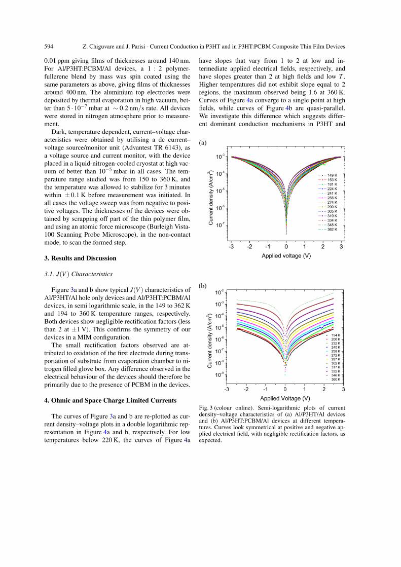
Figure 3a and b show typical J(V ) characteristics ofAl/P3HT/Al hole only devices and Al/P3HT:PCBM/Aldevices, in semi logarithmic scale, in the 149 to 362 Kand 194 to 360 K temperature ranges, respectively.Both devices show negligible rectification factors (lessthan 2 at ±1 V). This confirms the symmetry of ourdevices in a MIM configuration.
The small rectification factors observed are at-tributed to oxidation of the first electrode during trans-portation of substrate from evaporation chamber to ni-trogen filled glove box. Any difference observed in theelectrical behaviour of the devices should therefore beprimarily due to the presence of PCBM in the devices.
4. Ohmic and Space Charge Limited Currents
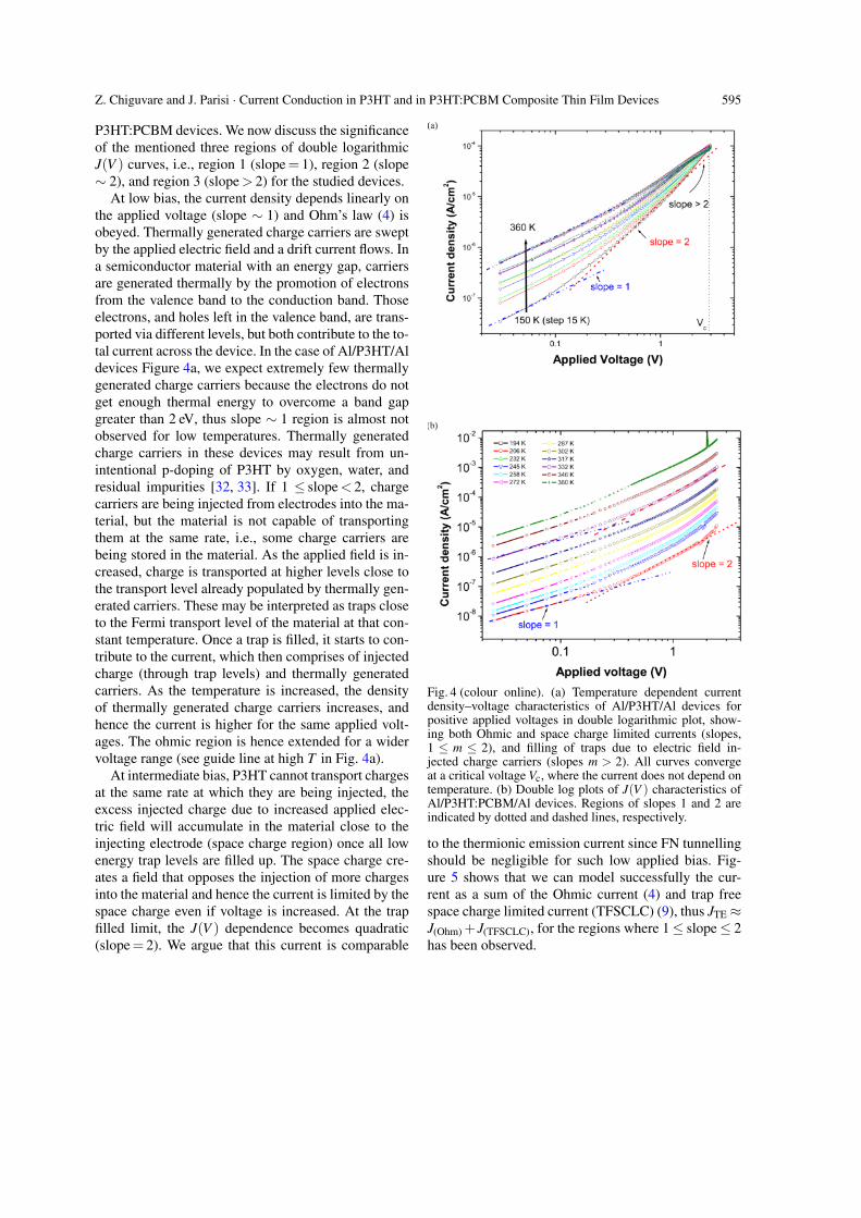
The curves of Figure 3a and b are re-plotted as cur-rent density–voltage plots in a double logarithmic rep-resentation in Figure 4a and b, respectively. For lowtemperatures below 220 K, the curves of Figure 4a
have slopes that vary from 1 to 2 at low and in-termediate applied electrical fields, respectively, andhave slopes greater than 2 at high fields and low T .Higher temperatures did not exhibit slope equal to 2regions, the maximum observed being 1.6 at 360 K.Curves of Figure 4a converge to a single point at highfields, while curves of Figure 4b are quasi-parallel.We investigate this difference which suggests differ-ent dominant conduction mechanisms in P3HT and
Fig. 3 (colour online). Semi-logarithmic plots of currentdensity–voltage characteristics of (a) Al/P3HT/Al devicesand (b) Al/P3HT:PCBM/Al devices at different tempera-tures. Curves look symmetrical at positive and negative ap-plied electrical field, with negligible rectification factors, asexpected.
Z. Chiguvare and J. Parisi · Current Conduction in P3HT and in P3HT:PCBM Composite Thin Film Devices 595
P3HT:PCBM devices. We now discuss the significanceof the mentioned three regions of double logarithmicJ(V ) curves, i.e., region 1 (slope = 1), region 2 (slope∼ 2), and region 3 (slope > 2) for the studied devices.
At low bias, the current density depends linearly onthe applied voltage (slope ∼ 1) and Ohm’s law (4) isobeyed. Thermally generated charge carriers are sweptby the applied electric field and a drift current flows. Ina semiconductor material with an energy gap, carriersare generated thermally by the promotion of electronsfrom the valence band to the conduction band. Thoseelectrons, and holes left in the valence band, are trans-ported via different levels, but both contribute to the to-tal current across the device. In the case of Al/P3HT/Aldevices Figure 4a, we expect extremely few thermallygenerated charge carriers because the electrons do notget enough thermal energy to overcome a band gapgreater than 2 eV, thus slope ∼ 1 region is almost notobserved for low temperatures. Thermally generatedcharge carriers in these devices may result from un-intentional p-doping of P3HT by oxygen, water, andresidual impurities [32, 33]. If 1 ≤ slope < 2, chargecarriers are being injected from electrodes into the ma-terial, but the material is not capable of transportingthem at the same rate, i.e., some charge carriers arebeing stored in the material. As the applied field is in-creased, charge is transported at higher levels close tothe transport level already populated by thermally gen-erated carriers. These may be interpreted as traps closeto the Fermi transport level of the material at that con-stant temperature. Once a trap is filled, it starts to con-tribute to the current, which then comprises of injectedcharge (through trap levels) and thermally generatedcarriers. As the temperature is increased, the densityof thermally generated charge carriers increases, andhence the current is higher for the same applied volt-ages. The ohmic region is hence extended for a widervoltage range (see guide line at high T in Fig. 4a).
At intermediate bias, P3HT cannot transport chargesat the same rate at which they are being injected, theexcess injected charge due to increased applied elec-tric field will accumulate in the material close to theinjecting electrode (space charge region) once all lowenergy trap levels are filled up. The space charge cre-ates a field that opposes the injection of more chargesinto the material and hence the current is limited by thespace charge even if voltage is increased. At the trapfilled limit, the J(V ) dependence becomes quadratic(slope = 2). We argue that this current is comparable
Fig. 4 (colour online). (a) Temperature dependent currentdensity–voltage characteristics of Al/P3HT/Al devices forpositive applied voltages in double logarithmic plot, show-ing both Ohmic and space charge limited currents (slopes,1 ≤ m ≤ 2), and filling of traps due to electric field in-jected charge carriers (slopes m > 2). All curves convergeat a critical voltage Vc, where the current does not depend ontemperature. (b) Double log plots of J(V ) characteristics ofAl/P3HT:PCBM/Al devices. Regions of slopes 1 and 2 areindicated by dotted and dashed lines, respectively.
to the thermionic emission current since FN tunnellingshould be negligible for such low applied bias. Fig-ure 5 shows that we can model successfully the cur-rent as a sum of the Ohmic current (4) and trap freespace charge limited current (TFSCLC) (9), thus JTE ≈J(Ohm) +J(TFSCLC), for the regions where 1≤ slope≤ 2has been observed.
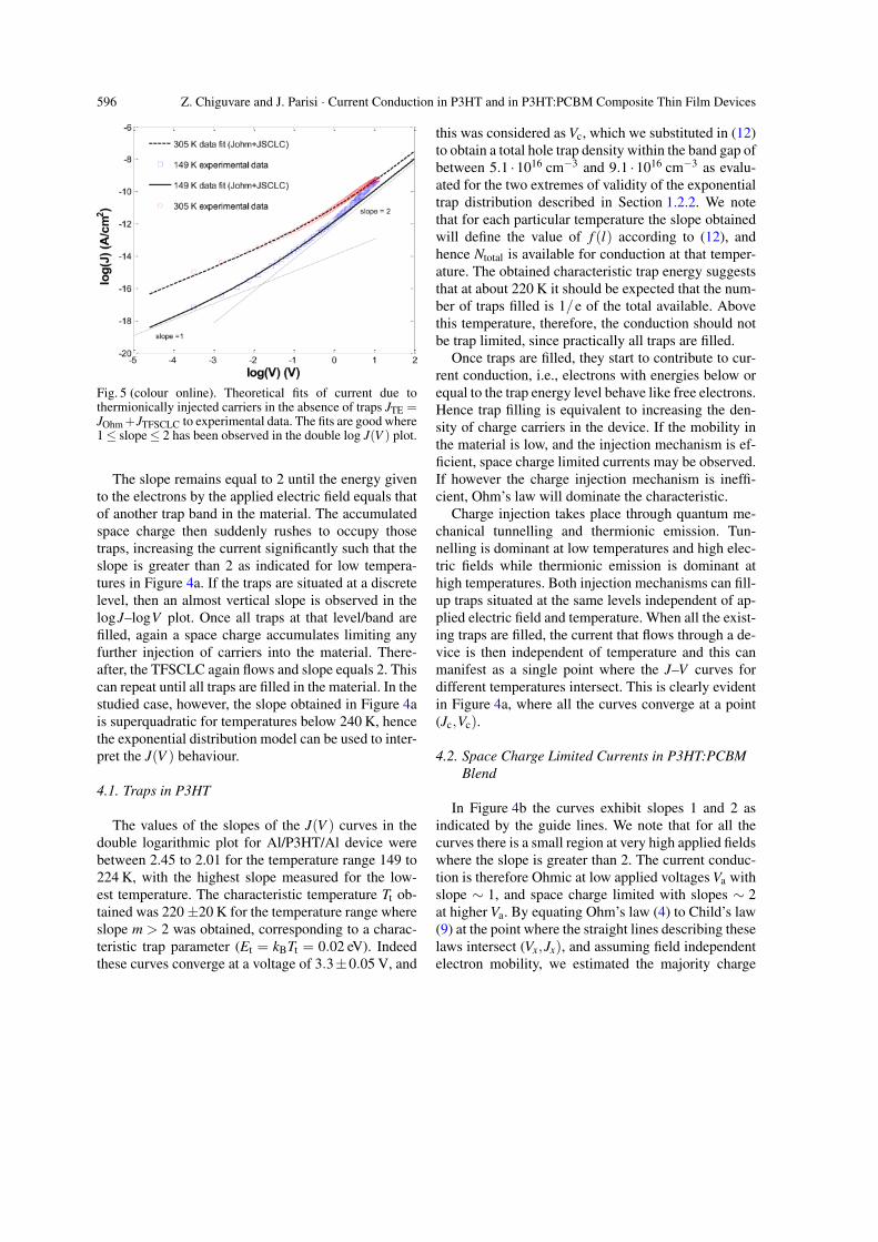
596 Z. Chiguvare and J. Parisi · Current Conduction in P3HT and in P3HT:PCBM Composite Thin Film Devices
Fig. 5 (colour online). Theoretical fits of current due tothermionically injected carriers in the absence of traps JTE =JOhm +JTFSCLC to experimental data. The fits are good where1≤ slope≤ 2 has been observed in the double log J(V ) plot.
The slope remains equal to 2 until the energy givento the electrons by the applied electric field equals thatof another trap band in the material. The accumulatedspace charge then suddenly rushes to occupy thosetraps, increasing the current significantly such that theslope is greater than 2 as indicated for low tempera-tures in Figure 4a. If the traps are situated at a discretelevel, then an almost vertical slope is observed in thelogJ–logV plot. Once all traps at that level/band arefilled, again a space charge accumulates limiting anyfurther injection of carriers into the material. There-after, the TFSCLC again flows and slope equals 2. Thiscan repeat until all traps are filled in the material. In thestudied case, however, the slope obtained in Figure 4ais superquadratic for temperatures below 240 K, hencethe exponential distribution model can be used to inter-pret the J(V ) behaviour.
4.1. Traps in P3HT
The values of the slopes of the J(V ) curves in thedouble logarithmic plot for Al/P3HT/Al device werebetween 2.45 to 2.01 for the temperature range 149 to224 K, with the highest slope measured for the low-est temperature. The characteristic temperature Tt ob-tained was 220±20 K for the temperature range whereslope m > 2 was obtained, corresponding to a charac-teristic trap parameter (Et = kBTt = 0.02 eV). Indeedthese curves converge at a voltage of 3.3±0.05 V, and
this was considered as Vc, which we substituted in (12)to obtain a total hole trap density within the band gap ofbetween 5.1 ·1016 cm−3 and 9.1 ·1016 cm−3 as evalu-ated for the two extremes of validity of the exponentialtrap distribution described in Section 1.2.2. We notethat for each particular temperature the slope obtainedwill define the value of f (l) according to (12), andhence Ntotal is available for conduction at that temper-ature. The obtained characteristic trap energy suggeststhat at about 220 K it should be expected that the num-ber of traps filled is 1/e of the total available. Abovethis temperature, therefore, the conduction should notbe trap limited, since practically all traps are filled.
Once traps are filled, they start to contribute to cur-rent conduction, i.e., electrons with energies below orequal to the trap energy level behave like free electrons.Hence trap filling is equivalent to increasing the den-sity of charge carriers in the device. If the mobility inthe material is low, and the injection mechanism is ef-ficient, space charge limited currents may be observed.If however the charge injection mechanism is ineffi-cient, Ohm’s law will dominate the characteristic.
Charge injection takes place through quantum me-chanical tunnelling and thermionic emission. Tun-nelling is dominant at low temperatures and high elec-tric fields while thermionic emission is dominant athigh temperatures. Both injection mechanisms can fill-up traps situated at the same levels independent of ap-plied electric field and temperature. When all the exist-ing traps are filled, the current that flows through a de-vice is then independent of temperature and this canmanifest as a single point where the J–V curves fordifferent temperatures intersect. This is clearly evidentin Figure 4a, where all the curves converge at a point(Jc,Vc).
4.2. Space Charge Limited Currents in P3HT:PCBMBlend
In Figure 4b the curves exhibit slopes 1 and 2 asindicated by the guide lines. We note that for all thecurves there is a small region at very high applied fieldswhere the slope is greater than 2. The current conduc-tion is therefore Ohmic at low applied voltages Va withslope ∼ 1, and space charge limited with slopes ∼ 2at higher Va. By equating Ohm’s law (4) to Child’s law(9) at the point where the straight lines describing theselaws intersect (Vx,Jx), and assuming field independentelectron mobility, we estimated the majority charge
Z. Chiguvare and J. Parisi · Current Conduction in P3HT and in P3HT:PCBM Composite Thin Film Devices 597
carrier mobility in the Al/P3HT:PCBM/Al devices atdifferent temperatures to be between 3.45 ·10−6 and5.76 ·10−5 cm2/Vs for the 194 K to 302 K temperaturerange. This method could not be used for Al/P3HT/Aldevices at lower temperatures because the slope equalto 1 region could not be observed, suggesting spacecharge limitation even at low voltages. We note alsothat the curves of Figure 4b are quasi parallel as op-posed to the convergent nature observed in Figure 4a.Therefore, we cannot assume an exponential distribu-tion of traps in P3HT:PCBM material blends.
Electron transport in a trap free molecularly dopedpolymer optimised for electron transport, such as ourAl/P3HT:PCBM/Al devices, involves a field drivenchain of redox reactions in which the carrier hops froma neutral molecule and its radical cation derivative.The electron transport process is triggered by an ini-tial charge transfer in which a neutral molecule, P3HT,is energetically favoured to donate an electron either toan adjacent metal contact or to the LUMO of PCBM.If the neutral transport molecule has an electron affin-ity higher than any competing species present, then thelatter is independent of their concentration, cannot actas traps; thus they are invisible to transiting electrons.A complementary situation can be described in termsof relative ionisation potentials for hole transportingsystems. These layers are therefore trap free insulatorswith finite unipolar mobility which means that whilethere are no intrinsic free carriers, an extrinsic carrieronce injected, will, under the influence of an electricfield, traverse the sample bulk without being locallyneutralised or immobilised.
We examined the nature of charge injection for thedevices in a bid to understand the origins of the dif-ferences in the nature of the observed behaviours (Sec-tion 5). It was then possible to obtain the mobility andcharge carrier densities in the whole temperature rangestudied, and therefore to compare and make conclu-sions on the conduction mechanisms in Al/P3HT/Aland Al/P3HT:PCBM/Al devices.
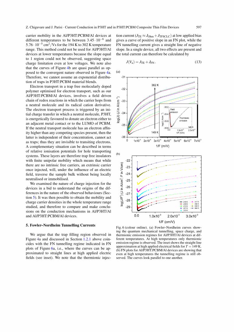
5. Fowler–Nordheim Tunnelling Currents
We argue that the trap filling region observed inFigure 4a and discussed in Section 1.2.1 above coin-cides with the FN tunnelling regime indicated in FNplots of Figure 6a, i.e., where the curves can be ap-proximated to straight lines at high applied electricfields (see inset). We note that the thermionic injec-
tion current (JTE ≈ JOhm +JTFSCLC) at low applied biasgives a curve of positive slope in an FN plot, while theFN tunnelling current gives a straight line of negativeslope. In a single device, all two effects are present andthe total current can therefore be calculated by
J(Va) = JTE + JFN . (13)
Fig. 6 (colour online). (a) Fowler–Nordheim curves show-ing the quantum mechanical tunnelling, space charge, andthermionic emission regimes for Al/P3HT/Al devices at dif-ferent temperatures. At high temperatures only thermionicemission regime is observed. The inset shows the straight lineapproximation at high applied electrical fields for T = 149 K.(b) FN plots for Al/P3HT:PCBM/Al devices are showing thateven at high temperatures the tunnelling regime is still ob-served. The curves look parallel to one another.

598 Z. Chiguvare and J. Parisi · Current Conduction in P3HT and in P3HT:PCBM Composite Thin Film Devices
Fig. 7 (colour online). FN curves at different temperaturesshowing data fits of a model that considers the total currentas the sum of Ohmic, TFSCLC, and FN tunnelling currents.
Equation (13) gives good data fits to single carrierJ(V ) experimental data as shown in Figure 7 forAl/P3HT/Al devices. The fitting hole mobilities forthe three curves considered here are 3.88, 4.00 and4.01 ·10−7 cm2/Vs, and charge carrier densities are8.7 ·1017 cm−3, 1.8 ·1018 cm−3, and 3.9 ·1018 cm−3,respectively, from low to high temperature. The ef-fective hole injection barrier in this case is obtainedas 0.88 eV for T = 149 K. We note that these holedensities are higher than the hole trap densities cal-culated in Section 4.1 above, indicating that both thetrap assisted hole tunnelling and thermionically emit-ted carriers contribute to the electrical conduction inAl/P3HT/Al devices.
We simulated the J(V ) characteristics of our devicesby using (13) and an in-house developed Matlab pro-gramme. For example by considering all factors con-stant and varying only the density of charge carriers,we obtained the curves in Figure 8a. If only the chargecarrier mobility is varied then we obtain the curves ofFigure 8b. Experimental data for AlP3HT/Al device at149 K is included with its theoretical fit for compar-ison purposes in both cases. The curves obtained inFigure 8a have a similar nature to the ones obtained ex-perimentally for the Al/P3HT/Al device (see Fig. 6a).We can therefore infer that the temperature dependentJ(V ) characteristics of Al/P3HT/Al devices in a FNplot show that the density of majority charge carriersin the bulk increases with increase in temperature. Thecharge carrier mobility of holes in this device is of the
Fig. 8 (colour online). (a) FN plots showing the effect of in-creasing charge carrier density due to increase in tempera-ture. The tunnelling regime becomes smaller as the tempera-ture increases. Space charge regime dominates conductivity.Notice how the curves come closer together with a uniformincrease of the density from 8.0 ·1017 to 5.0 ·1018 /cm3.(b) FN plots showing the effect of increasing charge car-rier mobility due to increase in temperature. The curves arequasi-parallel to each other.
order ∼ 4.0 ·10−7 cm2/Vs for the 149 to 224 K tem-perature range studied. The charge carrier mobility in-creases only slightly, up to ∼ 4.8 ·10−7 cm2/Vs for alltemperatures up to 362 K. The obtained mobilities areone to two orders smaller than the ones obtained byChoullis et al. [34] from time-of-flight photocurrentexperiments possibly due to the rigorous purificationprocedures to which they subjected their P3HT. It is
Z. Chiguvare and J. Parisi · Current Conduction in P3HT and in P3HT:PCBM Composite Thin Film Devices 599
known for instance that oxygen and residual impuri-ties can result in p-doping of polymers [32], and dif-ferences in nanomorphology of the blend [8] can sig-nificantly influence the result.
On the other hand, the J(V ) characteristics of theAl/P3HT:PCBM/Al device show thermal activationbehaviour, where the mobility is the main variable withtemperature. We note that the curves are quasi paralleland similar to the ones obtained where mobility is themain variable (cf. Fig. 6b and 8b). Electron mobilityis obtained from the fits to curves of Figure 6b to varyby three orders, i.e., from 4.5 ·10−7 to 2 ·10−4 cm2/Vsin the temperature range 194 to 360 K. We concludethat the charge carrier mobilities for Al/P3HT/Al de-vices are comparable to those of Al/P3HT:PCBM/Aldevices at low temperatures, but electron mobility be-comes significantly higher than hole mobility at roomtemperatures and above. Low charge carrier mobil-ities were also observed for pristine PPV and forP3HT, and our observation of higher electron mobil-ities in the blend is consistent with Brabec et al. [35].The obtained values are comparable to those obtainedby Shrotriya et al. [36] for their P3HT:PCBM blendswhere electron mobility was also found to be slightlyhigher than hole mobility. Electron and hole mobilities
in P3HT were found to be of the same order by Chouliset al. [34].
6. Conclusions
It has been shown that the trap assisted tunnellingcurrent in Al/P3HT/Al devices can be successfullymodelled as the sum of RS thermionic and FN tun-nelling currents. Further we established that the trans-port level in a P3HT:PCBM blend is the LUMOof PCBM which forms an Ohmic contact with alu-minium. We have shown that the hole carrier mobil-ity through HOMO of P3HT is more than two or-ders smaller than electron mobility through LUMO ofPCBM in a P3HT:PCBM blend thin film device. Suchdifferences in mobility mean that electrons can travelfaster than holes in the blend. This information is im-portant for the design of photovoltaic devices based onsuch polymer-fullerene blends.
Acknowledgements
Z. C. is grateful for the sponsorship offered by theGTZ and DAAD. All experiments were conducted atthe EHF University of Oldenburg.
[1] J. Shina, Organic Light Emitting Devices, A Survey,Springer Verlag, New York 2004.
[2] C. J. Brabec, V. Dyakonov, J. Parisi, and N. S. Sari-ciftci, Organic Photovoltaics: Concepts and Realiza-tion, Springer Series in Material Science, 60, SpringerVerlag, Berlin, Heidelberg 2003.
[3] T. Markvart and L. Castaner, Practical Handbook ofPhotovoltaics, Fundamentals and Applications, Else-vier Science Limited, Oxford 2003.
[4] C. Deibel and V. Dyakonov, Rep. Prog. Phys. 73,096401 (2010).
[5] C. D. Dimitrakopoulos and J. D. Mascaro, IBM J. Res.Dev. 45, 11 (2001).
[6] G. Dennler, M. C. Scharber, and C. J. Brabec, Adv.Mater. 21, 1323 (2009).
[7] W. Ma, C. Yang, X. Gong, K. Lee, and A. J. Heegar,Adv. Funct. Mater. 15, 1617 (2005).
[8] M. A. Green, K. Emery, Y. Hishikawa, and W. Warta,Prog. Photovolt. 19, 84 (2011).
[9] Y. Shen, M. W. Klein, D. B. Jacobs, J. C. Scott, andG. G. Malliaras, Phys. Rev. Lett. 86, 3867 (2001).
[10] M. Campoy-Quiles, T. Ferenczi, T. Agostinelli, P. G.Etchegoin, Y. Kim, T. D. Anthopoulos, P. N. Stavrinou,D. D. C. Bradley, and J. Nelson, Nat. Mat. 7, 158(2008).
[11] R. N. Marks, D. D. C. Bradley, R. W. Jackson, P. L.Burn, and A. B. Holmes, Synth. Met. 57, 4128 (1993).
[12] J. D. Parker, J. Appl. Phys. 75, 1656 (1994).[13] H. Vestweber, J. Pommerrehne, R. Sander, R. F. Mahrt,
A. Greiner, W. Heity and J. Baessler, Synth. Met. 68,263 (1995).
[14] P. E. Burrows and S. R. Forrest, Appl. Phys. Lett. 64,2285 (1993).
[15] E. Ettedgui, H. Razafitrimo, Y. Gao, and B. R. Hsieh,Appl. Phys. Lett. 67, 2705 (1995).
[16] P. W. M. Blom, M. J. M. de Jong, and J. J. M. Vlegaar,Appl. Phys. Lett. 68, 3308 (1996).
[17] P. W. M. Blom, M. J. M. de Jong, and M. G. van Mun-ster, Phys. Rev. B 55, R656 (1997).
[18] Z. Chiguvare, J. Parisi, and V. Dyakonov, J. Appl. Phys.94, 2440 (2003).
[19] K. C. Kao and W. Hwang, Electrical Transport inSolids, with Particular Reference to Organic Semicon-ductors, International Series in the Science of the SolidState, Vol. 14, Pergamon Press, Oxford 1981.
[20] M. A. Lambert and P. Mark, Current Injection in Solids,Academic, New York 1970.
[21] V. I. Arkhipov, P. Heremans, E. V. Emilianova, G. J.Adriaenssens, and H. Bassler, Appl. Phys. Lett. 82,3245 (2003).
600 Z. Chiguvare and J. Parisi · Current Conduction in P3HT and in P3HT:PCBM Composite Thin Film Devices
[22] V. Kumar, S. C. Jain, A. K. Kapoor, W. Geens, T. Aer-nauts, J. Poortmans, and R. Mertens, J. Appl. Phys. 92,7325 (2002).
[23] A. J. Campbell, M. S. Weaver, D. G. Lidzey, andD. D. C. Bradley, J. Appl. Phys. 84, 6737 (1998).
[24] W. P. Blom and M. C. J. M. Vissenberg, Mater. Sci.Eng. R27, 53 (2000).
[25] W. Brutting, S. Berleb, and A. G. Muckl, Org. Electron.2, 1 (2001).
[26] S. C. Jain, W. Geens, A. Mehra, V. Kumar, T. Aernouts,J. Poortmans, R. Mertens, and W. Willander, J. Appl.Phys. 89, 3804 (2001).
[27] Z. Chiguvare, and V. Dyakonov, Phys. Rev. B. 70,235207 (2004).
[28] S. J. Tans, R. G. Miedema, L. J. Geerligs, C. Dekker,J. Wu, D. Neher, and D. Wegner, Nanotechnol. 14, 1043(2003).
[29] D. Chirvase, Z. Chiguvare, M. Knipper, J. Parisi,V. Dyakonov, J. C. Hummelen, Synt. Met. 138, 299(2003).
[30] R. Valaski, L. M. Moreira, L. Micaroni, and I. A.Hummelgen, J. Appl. Phys. 92, 2035 (2002).
[31] M. Onoda, K. Tada, A. A. Zakhidov, and K. Yoshino,Thin Solid Films 331, 76 (1998).
[32] S. Karg, M. Meir, and W. Riess, J. Appl. Phys. 82, 1951(1997).
[33] Z. Chiguvare, J. Parisi, and V. Dyakonov, Z. Natur-forsch. 62a, 609 (2007).
[34] S. A. Choulis, Y. Kim, J. Nelson, D. D. C. Bradley,M. Giles, M. Shkunov, and I. McCulloch, Appl. Phys.Lett. 85, 3890 (2004).
[35] C. Brabec, V. Dyakonov, and U. Scherf, Organic Pho-tovoltaics, Materials, Device Physics and Manufactur-ing Technologies, Wiley VCH Verlag, Weinheim, 2008,p. 282 – 295, ISBN 978-3-527-31675-5.
[36] V. Shrotriya, Y. Yao, G. Li, and Y. Yang, Appl. Phys.Lett. 89, 063505 (2006).