Embed Size (px)
Citation preview

N.J. Pinto and R. PérezUniversity of Puerto Rico-Humacao, Humacao, Puerto Rico
C.H. MuellerAnalex Corporation, Brook Park, Ohio
N. Theofylaktos and F.A. MirandaGlenn Research Center, Cleveland, Ohio
Dual Input AND Gate Fabricated From a SingleChannel Poly (3–Hexylthiophene) Thin FilmField Effect Transistor
NASA/TM—2006-214015
May 2006
https://ntrs.nasa.gov/search.jsp?R=20060023348 2018-07-29T10:03:39+00:00Z

The NASA STI Program Office . . . in Profile
Since its founding, NASA has been dedicated tothe advancement of aeronautics and spacescience. The NASA Scientific and TechnicalInformation (STI) Program Office plays a key partin helping NASA maintain this important role.
The NASA STI Program Office is operated byLangley Research Center, the Lead Center forNASA’s scientific and technical information. TheNASA STI Program Office provides access to theNASA STI Database, the largest collection ofaeronautical and space science STI in the world.The Program Office is also NASA’s institutionalmechanism for disseminating the results of itsresearch and development activities. These resultsare published by NASA in the NASA STI ReportSeries, which includes the following report types:
• TECHNICAL PUBLICATION. Reports ofcompleted research or a major significantphase of research that present the results ofNASA programs and include extensive dataor theoretical analysis. Includes compilationsof significant scientific and technical data andinformation deemed to be of continuingreference value. NASA’s counterpart of peer-reviewed formal professional papers buthas less stringent limitations on manuscriptlength and extent of graphic presentations.
• TECHNICAL MEMORANDUM. Scientificand technical findings that are preliminary orof specialized interest, e.g., quick releasereports, working papers, and bibliographiesthat contain minimal annotation. Does notcontain extensive analysis.
• CONTRACTOR REPORT. Scientific andtechnical findings by NASA-sponsoredcontractors and grantees.
• CONFERENCE PUBLICATION. Collectedpapers from scientific and technicalconferences, symposia, seminars, or othermeetings sponsored or cosponsored byNASA.
• SPECIAL PUBLICATION. Scientific,technical, or historical information fromNASA programs, projects, and missions,often concerned with subjects havingsubstantial public interest.
• TECHNICAL TRANSLATION. English-language translations of foreign scientificand technical material pertinent to NASA’smission.
Specialized services that complement the STIProgram Office’s diverse offerings includecreating custom thesauri, building customizeddatabases, organizing and publishing researchresults . . . even providing videos.
For more information about the NASA STIProgram Office, see the following:
• Access the NASA STI Program Home Pageat http://www.sti.nasa.gov
• E-mail your question via the Internet [email protected]
• Fax your question to the NASA AccessHelp Desk at 301–621–0134
• Telephone the NASA Access Help Desk at301–621–0390
• Write to: NASA Access Help Desk NASA Center for AeroSpace Information 7121 Standard Drive Hanover, MD 21076

N.J. Pinto and R. PérezUniversity of Puerto Rico-Humacao, Humacao, Puerto Rico
C.H. MuellerAnalex Corporation, Brook Park, Ohio
N.Theofylaktos and F.A. MirandaGlenn Research Center, Cleveland, Ohio
Dual Input AND Gate Fabricated From a SingleChannel Poly (3–Hexylthiophene) Thin FilmField Effect Transistor
NASA/TM—2006-214015
May 2006
National Aeronautics andSpace Administration
Glenn Research Center

Available from
NASA Center for Aerospace Information7121 Standard DriveHanover, MD 21076
National Technical Information Service5285 Port Royal RoadSpringfield, VA 22100
This report contains preliminaryfindings, subject to revision as
analysis proceeds.
Available electronically at http://gltrs.grc.nasa.gov
NASA/TM—2006-214015 1
Dual Input AND Gate Fabricated From a Single Channel Poly(3-Hexylthiophene) Thin Film Field Effect Transistor
N.J. Pinto and R. Pérez
University of Puerto Rico-Humacao Department of Physics and Electronics
Humacao, Puerto Rico 00791
C.H. Mueller Analex Corporation
Brook Park, Ohio 44142
N. Theofylaktos and F.A. Miranda National Aeronautics and Space Administration
Glenn Research Center Cleveland, Ohio 44135
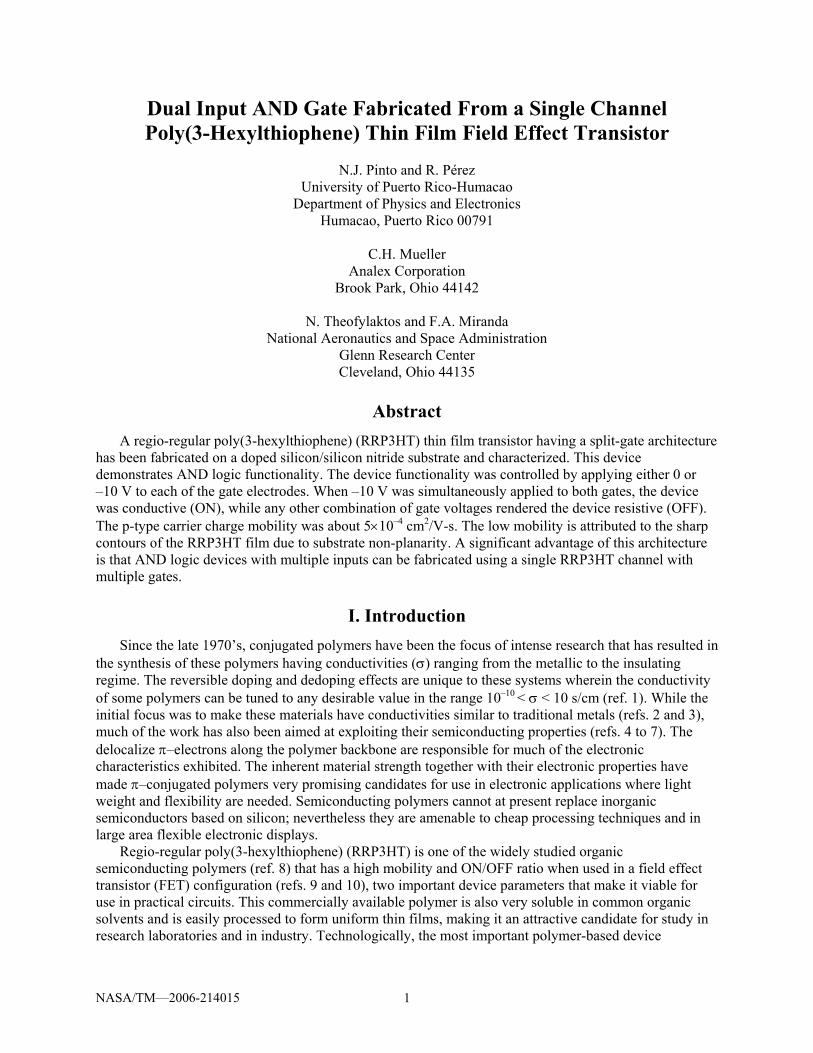
Abstract A regio-regular poly(3-hexylthiophene) (RRP3HT) thin film transistor having a split-gate architecture
has been fabricated on a doped silicon/silicon nitride substrate and characterized. This device demonstrates AND logic functionality. The device functionality was controlled by applying either 0 or –10 V to each of the gate electrodes. When –10 V was simultaneously applied to both gates, the device was conductive (ON), while any other combination of gate voltages rendered the device resistive (OFF). The p-type carrier charge mobility was about 5×10⁻⁴ cm2/V-s. The low mobility is attributed to the sharp contours of the RRP3HT film due to substrate non-planarity. A significant advantage of this architecture is that AND logic devices with multiple inputs can be fabricated using a single RRP3HT channel with multiple gates.
I. Introduction Since the late 1970’s, conjugated polymers have been the focus of intense research that has resulted in
the synthesis of these polymers having conductivities (σ) ranging from the metallic to the insulating regime. The reversible doping and dedoping effects are unique to these systems wherein the conductivity of some polymers can be tuned to any desirable value in the range 10–10 < σ < 10 s/cm (ref. 1). While the initial focus was to make these materials have conductivities similar to traditional metals (refs. 2 and 3), much of the work has also been aimed at exploiting their semiconducting properties (refs. 4 to 7). The delocalize π–electrons along the polymer backbone are responsible for much of the electronic characteristics exhibited. The inherent material strength together with their electronic properties have made π–conjugated polymers very promising candidates for use in electronic applications where light weight and flexibility are needed. Semiconducting polymers cannot at present replace inorganic semiconductors based on silicon; nevertheless they are amenable to cheap processing techniques and in large area flexible electronic displays.
Regio-regular poly(3-hexylthiophene) (RRP3HT) is one of the widely studied organic semiconducting polymers (ref. 8) that has a high mobility and ON/OFF ratio when used in a field effect transistor (FET) configuration (refs. 9 and 10), two important device parameters that make it viable for use in practical circuits. This commercially available polymer is also very soluble in common organic solvents and is easily processed to form uniform thin films, making it an attractive candidate for study in research laboratories and in industry. Technologically, the most important polymer-based device

NASA/TM—2006-214015 2
fabricated and studied is the FET since it forms the basic building block in logic circuits and switches for displays. Figure 1(a) shows a schematic cross-sectional view of the basic FET using an insulating gate dielectric layer over a doped silicon substrate. Two metal leads patterned over the insulator serve as the source and drain terminals of the device while the doped silicon serves as the global gate electrode. To complete the field effect transistor, an organic semiconducting channel is placed between the source and drain terminals either via electrochemical deposition (ref. 4), vacuum deposition (refs. 11 to 13), or spin coating (refs. 7, 9, and 14) of the semiconductor material resulting in a (2D) thin film morphology or via electrospinning resulting in a (1D) nanofibrous morphology (refs. 15 to 17). By connecting individual FET’s in tandem several types of logic gates can be fabricated and tested.
In this paper a modified FET architecture has been designed that uses a split gate configuration as shown in the schematic drawing of figure 1(b) so that each gate can be independently addressed. Our previous results on the use of such a design in the case of pentacene have now been extended to RRP3HT (ref. 18). We show that a spin coated RRP3HT single channel split-gate FET functions as a dual input logic AND gate. Since numerous logic circuits that require multiple inputs are widely used in devices such as comparators, the fact that this functionality can be achieved using a single transistor, rather than cascading a series of single input transistors could reduce the number of transistors required in many digital applications thereby making the circuits more compact. We correlate the measured electrical performance of this device with film morphology and substrate design.
II. Experiment A. Substrate Fabrication
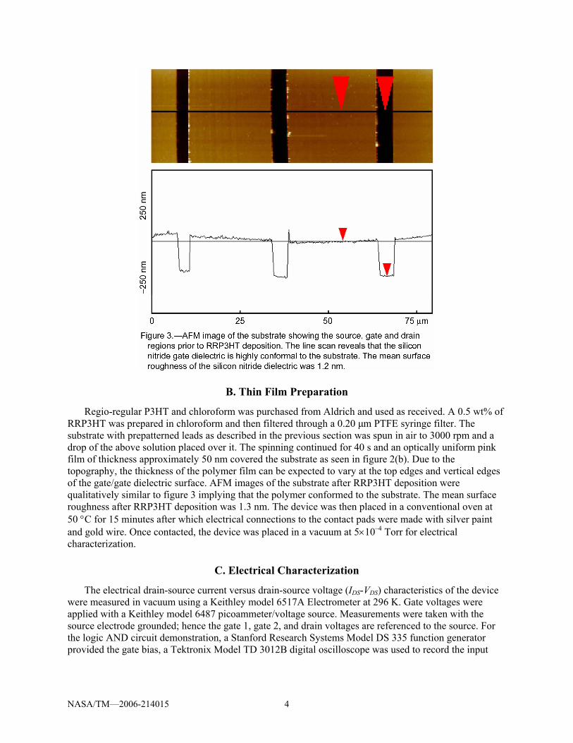
The device substrates were fabricated as follows: The starting wafer was n-type doped Si (10 -cm), with a 200 nm thick thermally grown oxide layer. First, the gate metals, comprised of 20 nm Cr/100 nm Au, were vacuum deposited in a thermal evaporator and patterned using conventional photolithographic and liftoff techniques. Next, a 100 nm thick silicon nitride film, Si3N4 (gate dielectric) was deposited over this using chemical vapor deposition (CVD). Access to the gate metallization was obtained by etching windows into the silicon nitride. Figure 2(a) shows an optical image of the substrate prior to deposition of the RRP3HT thin film as seen from the top, where leads ‘a’ and ‘b’ will correspond to the source and drain terminals, respectively, and leads ‘d’ and ‘e’ will correspond to the two gate electrodes. Electrode ‘c’ although present was not used. The source and drain metallization also comprised of 20 nm Cr/100 nm Au and was deposited on the CVD grown silicon nitride on either side of the buried split gates using conventional photolithographic and liftoff techniques. The electrode “fingers” were about 20 m wide and 600 m long. The spacing between the electrodes was ~4 m. Figure 2(b) shows the image of a similar substrate after spin coating it with a RRP3HT thin film. Due to the complex nature of the substrate fabrication process, the substrate planarity was checked by using an Atomic Force Microscope (AFM). Figure 3 shows an AFM image of a representative mid-section of the substrate prior to the semiconductor deposition, together with a section analysis of the image. As seen in figure 3, the CVD grown silicon nitride is highly conformal to the substrate topography with sharp edges at the boundaries of the electrodes. The vertical distance between the top of the silicon nitride/gate and the space between the gate and source terminal as indicated by the arrows along the line scan in figure 3 is approximately 125 nm. The mean surface roughness of the silicon nitride dielectric deposited on top of the gate metal was 1.2 nm. This implies that the substrate surface between the source and drain electrodes is not planar, as shown in the schematic representation of figure 1(b). AFM scans were taken in tapping mode using a Digital Instruments NanoScope IIIa Atomic Force Microscope.

NASA/TM—2006-214015 3
NASA/TM—2006-214015 4
B. Thin Film Preparation
Regio-regular P3HT and chloroform was purchased from Aldrich and used as received. A 0.5 wt% of RRP3HT was prepared in chloroform and then filtered through a 0.20 m PTFE syringe filter. The substrate with prepatterned leads as described in the previous section was spun in air to 3000 rpm and a drop of the above solution placed over it. The spinning continued for 40 s and an optically uniform pink film of thickness approximately 50 nm covered the substrate as seen in figure 2(b). Due to the topography, the thickness of the polymer film can be expected to vary at the top edges and vertical edges of the gate/gate dielectric surface. AFM images of the substrate after RRP3HT deposition were qualitatively similar to figure 3 implying that the polymer conformed to the substrate. The mean surface roughness after RRP3HT deposition was 1.3 nm. The device was then placed in a conventional oven at 50 °C for 15 minutes after which electrical connections to the contact pads were made with silver paint and gold wire. Once contacted, the device was placed in a vacuum at 5×10⁻⁴ Torr for electrical characterization.
C. Electrical Characterization
The electrical drain-source current versus drain-source voltage (IDS-VDS) characteristics of the device were measured in vacuum using a Keithley model 6517A Electrometer at 296 K. Gate voltages were applied with a Keithley model 6487 picoammeter/voltage source. Measurements were taken with the source electrode grounded; hence the gate 1, gate 2, and drain voltages are referenced to the source. For the logic AND circuit demonstration, a Stanford Research Systems Model DS 335 function generator provided the gate bias, a Tektronix Model TD 3012B digital oscilloscope was used to record the input

NASA/TM—2006-214015 5
gate bias and a second Keithley model 6517A Electrometer was used to record the output voltage that was measured across a 10 M load resistor.
III. Results The drain-source current (IDS) versus drain-source voltage (VDS) characteristics of the split-gate
transistor are shown in figure 4 for various combinations of gate voltages VGS1 and VGS2 which correspond to the voltage applied to the two buried gate electrodes lying in between the drain and source electrodes respectively, as seen in figure 2. For each scan, the bias on the gate electrodes was either 0 or –10 V, thus permitting four possible combinations of gate voltages. As seen from this figure, at VDS = –20 V the current is significantly higher only when both gate electrodes are biased simultaneously with –10 V. For the other combinations there was a smaller current primarily due to the intrinsic conductivity of RRP3HT and perhaps due to the unintentional doping in air. Similar results were also seen for other values of common gate bias voltages viz. IDS was higher only when both gates were biased high simultaneously. Thus this device has characteristics similar to a dual input logic AND gate. Due to the uneven substrate topography, especially at the step edges of the gate electrodes, the charge mobility in this device is adversely affected which in turn leads to inferior device characteristics. From figure 4 we can estimate this value from the linear portion of the curves corresponding to the common gate voltages of 0 and –10 V. The device transconductance (gm) is given by (refs. 19 and 20):
constVGS
DSm
DSVIg
=∂∂
= (1)
Treating the transistor as a single gate structure, with VGS1 = VGS2 = –10 V and at VDS = –1.0 V, gm is calculated to be 1.60×10⁻¹¹ s. The carrier mobility is then determined using:
Di
mVZCLg
=μ (2)
where L is the channel length (40 µm), Z is the channel width (600 µm), and Ci is the capacitance per unit area of the 100 nm thick silicon nitride layer (6.63×10⁻⁸ F/cm2 assuming a dielectric constant of 7.5). In the linear region, the mobility is calculated to be 1.5×10⁻⁵ cm2/V-s. The typical mobility of thin film RRRP3HT deposited on planar substrates is falls in the range 10–4–10–1 cm2/V-s (refs. 9 and 10). The low observed mobility is a result of the poor efficiency in charge transport due in part to the rapid evaporation of the solvent during film preparation and due to substrate non-planarity. This substrate non-planarity could lead to associated defects, charge traps and self localization of charge that act as barriers to charge transport.
In order to further characterize the device, a series of measurements having both gates biased with a common voltage has been done. Figure 5 shows the characteristic curves of this experiment. At low drain source voltages the channel current is linear but at voltages comparable to and larger than the gate-source bias, the drain-source current begins to saturate which is typical for polymer-based field effect transistors. True saturation is not seen in this particular device although it has been seen in other RRP3HT devices with split gate electrode configuration prepared under similar conditions. One reason could be the microscopic nature of the polymer contact with the gate dielectric and the conductivity of the polymer due to unintentional doping of the polymer while handled in air, which has been shown to have a detrimental effect on the FET behavior in RRP3HT (ref. 21). As seen in figure 5, the increase in IDS for fixed VDS upon increasing the negative gate bias demonstrates that the device operates as a FET and that the majority carriers are holes. At applied gate biases of –14 V on both gates, the ON/OFF ratio of this device was calculated to be ~30. The conductivity of the film in vacuum was found to be 4×10⁻⁸ s/cm under no

NASA/TM—2006-214015 6
gate bias conditions indicating some doping. The field effect charge mobility of this device was also calculated from the saturated section of the I-V curves using the standard FET equation:
2)(2 THGS
iDS VV
LZCI −
μ= (3)
where the various parameters have been defined earlier, and VTH represents the threshold voltage at which the conduction channel begins to be formed. Figure 6 shows the variation in the IDS versus VGS (with both the gates biased simultaneously to the same value) at a fixed drain-source voltage of –20 V. A corresponding plot of IDS
1/2 versus VGS is also shown in figure 6 from which we extract VTH = –8 V and the mobility as 5×10⁻⁴ cm2/V-s. Hysteresis effects are minimal although not totally absent as can be seen in figure 6 as the device was measured in vacuum and the shift in the threshold voltage was 1 V.

NASA/TM—2006-214015 7
One application of the split-gate architecture for logic circuitry is demonstrated via a two-input logic
AND circuit, shown schematically in the inset to figure 7. To create the device, a 10 MΩ load resistor was connected between ground and the transistor source terminal, with the two gate terminals serving as the inputs and the output (VR) was taken at the source terminal across the load resistor. A low frequency (0.01 Hz) square wave signal served as the input gate bias. For all combinations of VGS1 and VGS2 except VGS1 = VGS2 = –10 V, the transistor was in the resistive “OFF” state, and –0.3 mV < VR < 0 V. For VGS1 = VGS2 = –10 V, the transistor was in the more conductive “ON” state, causing a greater portion of the voltage drop to occur across the load resistor. As a result, VR is a more negative value (–2.0 mV < VR < –1.7 mV). The ability of the device to operate as an AND logic circuit is demonstrated in figure 7. The upper graph shows VGS1 and VGS2 as a function of time while the lower graph shows the corresponding change in the output voltage VR as a function of time for the four possible combinations of VGS1 and VGS2 = 0 or –10 V. Larger outputs were observed only when both gates were simultaneously biased “high”. Overshoots and undershoots in IDS were observed at the rising and falling edges of the gate bias due to the capacitive effects associated with sudden changes in the input signals. For practical applications, the magnitude of VR in the transistor “ON” (“OFF”) state must be increased (decreased) i.e., the dynamic ratio ION/IOFF must be increased. This can be achieved via the use of purified starting materials, pretreated substrates to make them more hydrophobic and hence have better contact with the semiconductor (reduced charge trapping) and substrates that possess more planar channel topologies, either by embedding the gate electrodes deeper into the gate dielectric prior to CVD growth of the upper dielectric or by using a thicker CVD grown gate dielectric that will minimize step coverage problems. As a simple model, our results can be explained by treating the device as consisting of two gate voltage controlled switches connected in series and which lead to the logical AND operation via the ON/OFF operation of these switches. The phenomena described in this paper can also be extended to other types of logic devices. For example, connecting the load resistor at the drain terminal and tapping the output between the drain terminal and ground is predicted to have the effect of producing NAND logic operation for the corresponding input gate biases.

NASA/TM—2006-214015 8
NASA/TM—2006-214015 9
IV. Summary A split-gate field effect transistor with a thin film of RRP3HT as the active semiconducting layer was
fabricated and characterized. This device was seen to work as a dual input logic AND gate and was operated by applying either 0 or –10 V to each of the gate electrodes. When –10 V was simultaneously applied to both gates, the device was conductive, while any other combination of gate voltages rendered the device resistive. The AND circuit was formed by placing a 10 MΩ resistor between the source terminal and ground. The device also worked as a field effect transistor with a dynamic ratio of ~30 and had a charge carrier mobility of 5×10⁻⁴ cm2/V-s. These device parameters are expected to improve via the use of purified starting materials, pretreated substrates and more planar channel topography. A significant advantage of this device is that AND logic devices with multiple inputs can be built using a single RRP3HT channel with multiple gates.
References 1. J.-C. Chiang and A.G. MacDiarmid, Synth. Metals 13, 193 (1986). 2. Y. Cao, P. Smith, and A.J. Heeger, Synth. Metals 48, 91–97 (1992). 3. P.N. Adams, P.J. Laughlin, and A.P. Monkman, Solid State Commun. 91, 875–878 (1994).
Tsumura, H. Koezuka, and T. Ando, Appl. Phys. Lett. 49, 1210 (1986). 4. J.H. Burroughes, C.A. Jones, and R.H. Friend, Nature 335, 137 (1988). 5. G. Horowitz, D. Fichou, X. Peng, and F. Garnier, Synth. Metals 41–43, 1127 (1991). 6. A.R. Brown, C.P. Jarret, D.M. de Leeuw, and M. Matters, Synth. Metals 88, 37 (1997). 7. T-An Chen, X. Wu, and R.D. Rieke, J. Am. Chem. Soc. 117, 233 (1995). 8. Z. Bao, A. Dodabalapur, and A.J. Lovinger, Appl. Phys. Lett. 69, 4108 (1996). 9. H. Sirringhaus, N. Tessler, and R.H. Friend, Science 280, 1741 (1998). 10. F. Garnier, R. Hajlaoui, A. Yassar, and P. Srivastava, Science 265, 1684 (1994).
Dodabalapur, L. Torsi, and H.E. Katz, Science 268, 207 (1995). 11. J. Zaumseil, T. Someya, Z. Bao, Y.L. Loo, R. Cirelli, and J.A. Rogers, Appl. Phys. Lett. 82, 793
(2003). 12. M. Halik, H. Klauk, U. Zschieschang, T. Kriem, G. Schmid, W. Radik, and K. Wussow, Appl. Phys.
Lett. 81, 289 (2002). 13. N.J. Pinto, A.T. Jonson Jr., A.G. MacDiarmid, C.H. Mueller, N. Theofylaktos, D.C. Robinson, and
F.A. Miranda, Appl. Phys. Lett. 83, 4244 (2003). 14. R. Gonzalez and N.J. Pinto, Synth. Metals 151, 275 (2005).
Babel, D. Li, Y. Xia, and S.A. Jenekhe, Macromolecules 38, 4705 (2005). 15. C.H. Mueller, N. Theofylaktos, F.A. Miranda, A.T. Johnson, Jr., and N.J. Pinto, Thin Solid Films
496, 494 (2006). 16. C. Dimitrakopoulos and P. Malenfant, Adv. Mat. 14, 99 (2002). 17. S. Scheinert and G. Paasch, Phys. Stat. Sol. (a) 6, 1263 (2004). 18. S. Hoshino, M. Yoshida, S. Uemura, T. Kodzasa, N. Takada, T. Kamata, and K. Yase, Appl. Phys.
Lett. 95, 5088 (2004).

This publication is available from the NASA Center for AeroSpace Information, 301–621–0390.
REPORT DOCUMENTATION PAGE
2. REPORT DATE
19. SECURITY CLASSIFICATION OF ABSTRACT
18. SECURITY CLASSIFICATION OF THIS PAGE
Public reporting burden for this collection of information is estimated to average 1 hour per response, including the time for reviewing instructions, searching existing data sources,gathering and maintaining the data needed, and completing and reviewing the collection of information. Send comments regarding this burden estimate or any other aspect of thiscollection of information, including suggestions for reducing this burden, to Washington Headquarters Services, Directorate for Information Operations and Reports, 1215 JeffersonDavis Highway, Suite 1204, Arlington, VA 22202-4302, and to the Office of Management and Budget, Paperwork Reduction Project (0704-0188), Washington, DC 20503.
NSN 7540-01-280-5500 Standard Form 298 (Rev. 2-89)Prescribed by ANSI Std. Z39-18298-102
Form Approved
OMB No. 0704-0188
12b. DISTRIBUTION CODE
8. PERFORMING ORGANIZATION REPORT NUMBER
5. FUNDING NUMBERS
3. REPORT TYPE AND DATES COVERED
4. TITLE AND SUBTITLE
6. AUTHOR(S)
7. PERFORMING ORGANIZATION NAME(S) AND ADDRESS(ES)
11. SUPPLEMENTARY NOTES
12a. DISTRIBUTION/AVAILABILITY STATEMENT
13. ABSTRACT (Maximum 200 words)
14. SUBJECT TERMS
17. SECURITY CLASSIFICATION OF REPORT
16. PRICE CODE
15. NUMBER OF PAGES
20. LIMITATION OF ABSTRACT
Unclassified Unclassified
Technical Memorandum
Unclassified
National Aeronautics and Space AdministrationJohn H. Glenn Research Center at Lewis FieldCleveland, Ohio 44135–3191
1. AGENCY USE ONLY (Leave blank)
10. SPONSORING/MONITORING AGENCY REPORT NUMBER
9. SPONSORING/MONITORING AGENCY NAME(S) AND ADDRESS(ES)
National Aeronautics and Space AdministrationWashington, DC 20546–0001
Available electronically at http://gltrs.grc.nasa.gov
May 2006
NASA TM—2006-214015
E–15215
WBS 953033.01.03.06
15
Dual Input AND Gate Fabricated From a Single Channel Poly(3–Hexylthiophene) Thin Film Field Effect Transistor
N.J. Pinto, R. Pérez, C.H. Mueller, N. Theofylaktos, and F.A. Miranda
Poly (3–Hexylthiophene); Logic gate; JFET
Unclassified -UnlimitedSubject Categories: 88 and 91
N.J. Pinto and R. Pérez, University of Puerto Rico-Humacao, Department of Physics and Electronics, Humacao,Puerto Rico 00791; C.H. Mueller, Analex Corporation, 1100 Apollo Drive, Brook Park, Ohio 44142; N. Theofylaktosand F.A. Miranda, NASA Glenn Research Center. Responsible person, F.A. Miranda, organization codeRCA, 216–433–6589.
A regio-regular poly (3-hexylthiophene) (RRP3HT) thin film transistor having a split-gate architecture has beenfabricated on a doped silicon/silicon nitride substrate and characterized. This device demonstrates AND logicfunctionality. The device functionality was controlled by applying either 0 or –10 V to each of the gate electrodes. When–10 V was simultaneously applied to both gates, the device was conductive (ON), while any other combination of gatevoltages rendered the device resistive (OFF). The p-type carrier charge mobility was about 5x10⁻⁴ cm2/V-sec. The lowmobility is attributed to the sharp contours of the RRP3HT film due to substrate non-planarity. A significant advantage ofthis architecture is that AND logic devices with multiple inputs can be fabricated using a single RRP3HT channel withmultiple gates.