Embed Size (px)
Citation preview

Evaluation of transport properties in poly(3-hexylthiophene)
using SCLC method and Controlled-Overflow-Transistor
Mohammad Fareed Ahmed
Orientador
Prof. Dr. Ivo Alexandre Hümmelgen
Group of Organic Optoelectronic Devices,
Departamento de Física,
Universidade Federal do Paraná.
Curitiba-2013

“ Você acha ou você sabe?......
It’s so simple………”
Professor Dr. I. A. Hümmelgen

Abstract
Since the discovery of conducting polymers in 1977, a new era of research work has escalated,
with applications such as transistors, solar cells, logic circuits, sensors, etc. The materials can be
chemically modified during their synthesis in order to tailor the desired mechanical, electronic and
optical properties of the final product. However, one of the main limitations of organic materials is
due to the combination of its low mobility, presence of traps and unbalanced mobilities between
positive and negative charge carriers. Several methods have been employed to determine the
mobility such as time-of-light, field-effect transistor, etc.
The work presented in this thesis focuses on utilizing a simple method called Space-
Charge-Limited current (SCLC) to determine the mobility of carriers in poly(3-hexylthiophene)
(P3HT). P3HT is one of the most studied organic semiconductor polymer due to its high positive
charge carrier mobility, good solubility and processability. Its positive charge carrier mobility has
been evaluated by several methods including SCLC. However, the knowledge of its negative
charge mobility is limited. In this work, we have investigated both the positive and negative charge
carrier mobilities utilizing the SCLC method. Finally, the obtained values are compared to the
obtained values by other methods that have already determined both of these mobilities.
Further, this work also sheds a new light on further enhancing the applications of low-
mobility conducting polymers by using it in simple, cost effective hybrid transistor architecture.
This transistor takes the advantage of the low mobility in conducting polymers and involves two
regimes of operation at low and high electric field strengths. At low electric field, SCLC regime is
formed and at high electric field strength thermionic regime is encountered. To our knowledge,
this is one of a kind architecture. The device operation mainly depends upon the properties of the
conducting polymer in use.

Resumo Estendido
Os objetivos deste trabalho de tese são: (і) avaliar as propriedades de transporte do poly(3-
hexylthiophene) (P3HT) utilizando o método de corrente limitada por carga espacial (SCLC); (іі)
fabricar e caracterizar um transistor que denominamos Controlled-Overflow-Transistor (COT).
Para isso, propomos um novo conceito de transistor, com base em SCLC e fenômenos emissão
termiônica.
Esta tese está dividida em três seções: (1) Introdução e propriedades eletrônicas de
semicondutores orgânicos, onde é apresentada uma visão geral do conceito de mobilidade de
portadores de carga em semicondutores orgânicos, para estudar as interfaces entre eletrodos
metálicos e semicondutores, e que inclui tanto SCLC e conceitos emissão termiônica. (2)
Motivação e objetivo por detrás do uso de método SCLC para determinar as propriedades de
transporte em P3HT. Em seguida é apresentado o método de fabricação e caracterização elétrica
dos diodos para calcular os portadores de carga positivos e negativos no P3HT. Finalmente,
resultados e discussões baseados em resultados obtidos dos dispositivos. (3) Introdução sobre o
novo conceito de transistor COT. Seguido pelo método de fabricação e caracterização elétrica dos
transistores e resultados e discussões baseados em resultados obtidos dos transistores.
Semicondutores orgânicos são úteis para uma ampla gama de aplicações, devido à sua
combinação de propriedades eletrônicas e óticas de semicondutores com propriedades mecânicas e
de processabilidade de polímeros. O Capítulo 1 apresenta uma visão geral das propriedades de
semicondutores orgânicos. Estes têm muitas vantagens, tais como a fácil fabricação, flexibilidade
mecânica, baixo custo, etc. No entanto, a limitação principal é a baixa mobilidade de portadores, o
que dificulta as suas aplicações em que são necessários alta velocidade e desempenho. A baixa
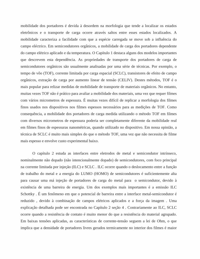
mobilidade dos portadores é devida à desordem na morfologia que tende a localizar os estados
eletrônicos e o transporte de carga ocorre através saltos entre esses estados localizados. A
mobilidade caracteriza a facilidade com que a espécie carregada se move sob a influência do
campo eléctrico. Em semicondutores orgânicos, a mobilidade de carga dos portadores dependente
do campo elétrico aplicado e da temperatura. O Capítulo 1 destaca alguns dos modelos importantes
que descrevem esta dependência. As propriedades de transporte dos portadores de carga de
semicondutores orgânicos são usualmente analisadas por uma série de técnicas. Por exemplo, o
tempo de vôo (TOF), corrente limitada por carga espacial (SCLC), transistores de efeito de campo
orgânicos, extração de carga por aumento linear de tensão (CELIV). Destes métodos, TOF é o
mais popular para relizar medidas de mobilidade de transporte de materiais orgânicos. No entanto,
muitas vezes TOF não é prático para avaliar a mobilidade dos materiais, uma vez que requer filmes
com vários micrometros de espessura. É muitas vezes difícil de replicar a morfologia dos filmes
finos usados nos dispositivos nos filmes espessos necessários para as medições de TOF. Como
consequência, a mobilidade dos portadores de carga medida utilizando o método TOF em filmes
com diversos micrometros de espessura poderia ser completamente diferente da mobilidade real
em filmes finos de espessuras nanométricas, quando utilizado no dispositivo. Em nossa opinião, a
técnica de SCLC é muito mais simples do que o método TOF, uma vez que não necessita de filme
mais espesso e envolve custo experimental baixo.
O capítulo 2 estuda as interfaces entre eletrodos de metal e semicondutor intrínseco,
nominalmente não dopado (não intencionalmente dopado) de semicondutores, com foco principal
na corrente limitada por injeção (ILC) e SCLC . ILC ocorre quando o deslocamento entre a função
de trabalho do metal e a energia do LUMO (HOMO) de semicondutores é suficientemente alta
para causar uma má injeção de portadores de carga do metal para o semicondutor, devido à
existência de uma barreira de energia. Um dos exemplos mais importantes é a emissão ILC
Schottky . É um fenômeno em que o potencial de barreira entre a interface metal-semicondutor é
reduzido , devido à combinação de campos elétricos aplicados e a força da imagem . Uma
explicação detalhada pode ser encontrada no Capítulo 2 seção 4 . Contrariamente ao ILC, SCLC
ocorre quando a resistência de contato é muito menor do que a resistência do material agrupado.
Em baixas tensões aplicadas, as características de corrente-tensão seguem a lei de Ohm, o que
implica que a densidade de portadores livres gerados termicamente no interior dos filmes é maior

do que a dos portadores injetados. A densidade de corrente na região condutora é dada por
dVqnJ 0 , onde 0
n é a concentração de elétrons livres no equilíbrio térmico (considerando-
se apenas de elétrons), μ é a mobilidade do portador de carga , V é a tensão aplicada e d é a
espessura da amostra . Com o aumento da tensão, a densidade dos portadores injetados se torna
comparável com a densidade de portadores livres gerados termicamente, o mecanismo SCLC
torna-se perceptível e a curva corrente- tensão sofre alterações em suas características. Portanto, o
início da SCLC tem lugar quando as características da corrente-tensão começam a passagem da lei
de Ohm para o regime da SCLC . A tensão de início é dada por 2
098 dqnVΩ onde ε é a
permeabilidade absoluta do semicondutor. Com a continuação do aumento de tensão, mais elétrons
(ou buracos) são injetados a partir do metal para o semicondutor. Devido à baixa mobilidade dos
semicondutores orgânicos, estes elétrons são acumulados perto da interface metal-semicondutor e
previnem mais injeção de elétrons. Em outras palavras, a corrente é limitada pela sua própria carga
no espaço, o que por sua vez reduz o campo elétrico no elétrodo de injeção para zero. A blindagem
devido a estas "catgas espaciais" produz características não lineares de corrente-tensão. Nesta
região, a densidade de corrente , 32 89 dVJ é dada pela lei de Mott-Gurney para o caso de
tipo único de portadores e ausência armadilhas.
Resumindo, para a região condutora, J é proporcional a , onde n é o coeficiente angular
da curva ajustada, e no caso da região ôhmica n 1 e para da região SCLC n 2. No, capítulo 2,
seção 5, são derivadas as expressões matemáticas de densidade de corrente ôhmica, ponto de
cruzamento e regiões SCLC. Além disso, um contato ôhmico (ou quase-ôhmico) na interface
metal-semicondutor, é importante para ocorrer uma injecção de carga unipolar que permita medir a
mobilidade do portador na região SCLC. A injecção unipolar pode ser obtida ajustando a diferença
entre a função-trabalho do metal e a energia do LUMO (HUMO) do semicondutor orgânico, ver
Capítulo 2 seção 6.
O objetivo deste projeto é a avaliação da mobilidade de portadores de carga positivas e
negativas, ou seja, buracos e elétrons, respectivamente, o P3HT regio-regular (RR-P3HT), usando
o método SCLC. Anteriormente, o método TOF foi usado para calcular as mobilidades dos
portadores de carga no RR-P3HT, mas segundo nosso conhecimento, até agora só a mobilidade de
portadores positivos foi calculada utilizando o método de SCLC. Finalmente, a comparação

também será feita com mobilidades obtidas anteriormente por TOF. Para avaliar a mobilidade dos
portadores de cargas positivos, apenas a mobilidade de configuração de diodo é usado com RR-
P3HT entre ITO / PEDOT: PSS e Al foi utilizada. O princípio básico de operação envolve a
injeção de buracos do ITO/PEDOT:PSS no RR-P3HT enquanto forma uma barreira de injeção de
elétrons, sendo esta uma barreira de alta energia potencial entre o nível de Fermi de Al e o LUMO
do P3HT. Desta forma, apenas os buracos são injetados no RR-P3HT, tendo somente a medida das
mobilidades de portadores de carga positivos. O capítulo 3 seção 5 explica o princípio de
funcionamento dos diodos em detalhe. A análise do gráfico log-log das características de corrente
× tensão do diodo com ITO/PEDOT: PSS dá uma região ôhmica (n 1) e uma região SCLC (n
2) em tensões baixas e altas, respectivamente. Substituindo o valor de VΩ como a tensão do início
de SCLC, 2
098 dqpVΩ , obtém-se o valor de 0p = 1.68 × 10¹⁶
cm-3
. O próximo passo foi
calcular a mobilidade dos buracos. A mobilidade pode ser calculada usando-se dVqpJ h0
que dá um valor de µh = 1,16 × 10⁻⁴
cm2/Vs e para a região de SCLC a mobilidade de buracos
pode ser calculada utilizando 32 89 dVJ o que dá um valor de µh = 1,35 × 10⁻⁴
cm2/Vs. O
capítulo 3 seção 6 cobre a parte dos cálculos.
Para avaliar somente a mobilidade de portadores de carga negativos, é usada uma
configuração de diodo com RR-P3HT entre Al / CsO (de cima) e Al / CsO (inferior). O princípio
básico de operação envolve a injeção de buracos de elétrons por cima, no Al/CsO como no RR-
P3HT, enquanto forma-se uma barreira de injeção de buracos, sendo esta uma alta barreira de
energia potencial entre o nível de Fermi do Al/CsO e HOMO do RR-P3HT. Desta forma só
elétrons são injetados estão no RR-P3HT e a avaliação de mobilidades será somente de portadores
de carga negativa. A análise das características de corrente×tensão do diodo dá uma região ôhmica
(n 1) e uma região SCLC (n 2) em tensões baixas e altas, respectivamente. Da tensão
2
098 dqnVΩ , obtém-se o valor de 0n = 3,36 × 10¹⁶
cm-3
. A mobilidade no regime ôhmico
pode então ser calculada usando-se dVqnJ h0 , que dá um valor de µe = 1,71 × 10⁻⁹
cm2/Vs e
para a região SCLC 32 89 dVJ , o que dá um valor de µe = 1,93 × 10⁻⁹
cm2/Vs.

A conclusão tirada partir dos resultados acima é que, embora as concentrações de
portadores de carga gerados termicamente para ambos os portadores são da mesma ordem de
grandeza, , i.e. 0p 0n 1016
cm-3
à temperatura ambiente, com base nos valores de mobilidade o
transporte de portadores de carga positivas é muito mais eficiente do que os portadores de carga
negativas no RR-P3HT. Observou-se que quando o RR-P3HT é exposto ao oxigênio e à água, a
mobilidade dos portadores de carga negativa é reduzida em quatro ordens de grandeza, mas,
curiosamente, a mobilidade dos portadores de carga positiva permanece quase inalterada.
O segundo objetivo objetivo deste trabalho é o de fabricar e caracterizar eletricamente o
transistor COT. Para contornar o problema da baixa mobilidade dos semicondutores orgânicos, a
aplicação de transistores orgânicos que necessitam de correntes de saída alta é realizada através da
utilização de dispositivos em arquitetura vertical. Aqui, os portadores de carga se movem através
do dispositivo perpendicularmente ao substrato e, portanto, tem que viajar distância da ordem da
espessura do filme, tipicamente inferior a um micrômetro. O capítulo 4, seção 2, tem uma breve
descrição dos transistores com base em materiais semicondutores em arquitetura vertical. Neste
trabalho, o desempenho dos transistores é ainda melhorado usando uma família diferente de
transistores que foram denominados como COT. O conceito básico do COT tira vantagem da
baixa mobilidade dos portadores em polímeros condutores. Pelo nosso conhecimento, este
conceito é completamente novo e nunca foi testado antes. Nele, polianilina sulfonada (Span), um
polímero condutor auto-dopado, é utilizado como o semicondutor/condutor. Foi encontrado,
usando a teoria funcional da densidade (DFT) que o LUMO e HOMO de SPAN estão em torno de
3,7 eV e 4,7 eV em relação ao nível de vácuo, respectivamente. Além disso, estados eletrônicos
desocupados foram encontrados muito perto de 3,65 eV.
A fabricação de COT envolve a deposição de SPAN com uma espessura t é depositada por
polimerização química no topo de Si tipo n. Depois Al por sublimação térmica como terminais
fonte (S) e de controle (CT), com uma distância L entre os eletrodos foram depositados. A
relação entre L e t é escolhida de forma que que L >> t.
A interface Al/SPAN é conhecida por formar um contato quase-ôhmico, ao passo que a
SPAN/n-Si é conhecida por formar um contato Schottky. Sobre a aplicação do potencial reverso
os elétrons são injetados a partir da fonte na SPAN. Devido à alta resistividade (medida pelo
método de quatro pontas) e a baixa mobilidade dos portadores na SPAN, os elétrons se acumulam
perto do contato de injeção . Com a pequena espessura da camada de SPAN, devido à repulsão
eletrostática entre os portadores de carga injetados, elétrons tendem a espalhar-se ao longo da
camada de SPAN na direção perpendicular à interface Al/SPAN. Estes elétrons acumulados
tendem a preencher os estados eletrônicos desocupados da SPAN. A ocupação desses estados
eletrônicos pode ser alta o suficiente para que os elétrons possam adquirir uma energia potencial
suficiente para superar a barreira de energia Schottky na interface SPAN/n-Si. O campo elétrico
presente na barreira Schottky então dirige os portadores de carga para o terminal n-Si. Portanto, o
fluxo de elétrons pode ser amplificado pelo controle da quantidade de injeção de elétrons do Al
para SPAN. Observamos também que o dispositivo pode ser otimizado através da variação do
comprimento do canal e espessura da camada de SPAN. Com base nas características do
dispositivo, foi observado que o ganho de corrente é quase quatro vezes mais elevado em
comparação com outros transistores baseados em materiais orgânicos semicondutores em
arquitetura vertical. No entanto, sofre de uma corrente de fuga elevada. Assim, mesmo sendo o
COT útil para aplicações de baixa tensão, mas a corrente de fuga elevada pode causar elevada
dissipação de energia.

Acknowledements
This licentiate thesis is hopefully a step towards my final Ph.D. I could not have
come this far on my own. I would like to take this opportunity to express my
sincerest thanks to the following people:
Prof. Dr. Ivo A. Hümmelgen, my award-winning professor, for giving me this
opportunity to work in a constantly evolving field of science and for always being
the source of inspiration.
Prof. Dr. Michelle , Prof. Dr. Marlus and Prof. Dr. Serbena, the three Organic
Electronic wiz’s, for always taking the time to help, whatever the problem or
question may be and for the valuable discussions. Zé, wanna play LFD2?
Prof. Dr. Regina for helping me with Sulfonated polyaniline preparation and for the
guidance.
The entire of group of Organic Optoelectronic devices ( at this date IVO, Michelle,
Marlus, Serbena, Marcia, Bruno, Diana, Cris, Ana, Rafael and previous members
including Wagner, Keli, Lucieli).
My family for always has been there for me even in long separation times.
Last, but not least, CNPQ for research grant.
Contents
1. Introduction 1
1. Organic Electronics 1
2. Properties of organic semiconductors 1
3. Conduction in small molecules and polymers 3
4. Charge transport in disordered organic semiconductors 5
5. Charge carrier mobility 6
6. Charge carrier mobility measurement methods 9
2. Charge injection 11
1. Introduction 11
2. Interface barrier formation 11
3. Contact barrier types 13
4. Blocking/injected limited current (ILC) 14
5. Space-charge-limited current (SCLC) 18
6. SCLC mobility 24
3. Evaluation of transport properties in region-regular poly(3-
hexylthiophene) using SCLC method 28
1. Introduction 28

Contents
2. Poly(3-hexylthiophene) 28
3. Motivation 29
4. Fabrication 30
5. Principle of operation 32
6. Results and Discussions 34
7. Conclusions 39
8. Future work 39
4. Controlled-Overflow-Transistor (COT) 40
1. Introduction 40
2. Transistors based on semiconducting materials 41
3. Motivation 44
4. Self-doped sulfonated polyaniline (SPAN) 45
5. COT fabrication 56
6. Junction characteristics 58
7. Results and Discussions 60

Contents
8. Current gain 70
9. Conclusions 72
10. Future work 73
References і

List of Figures
1. Scheme for the orbitals and bonds for two 2sp - hybridized carbon atoms, where σ - bonds are
formed by overlapping of 2sp - orbitals and π- bonds are formed by side-to-side overlapping of pz-
orbitals 2
2. Simplified illustration of a polaron. As the electron moves through the organic material, it attracts
positive ions. This lattice distortions travels with the electron. 3
3. Energy level shifts throughout the material because of the local disorder. LUMO and HOMO may
be approximated by a Gaussian density of states. Hopping of electrons occurs through the LUMO
(blue) and of holes through the HOMO (red). 6
4. Formation of interface energy barrier between a metal and an intrinsic semiconductor. The picture
shows the formation of a contact barrier for the pure and defect free contacts. The energy barrier is
given by Φb = ΦM - χ. 13
5. Shows two barriers types for an intrinsic semiconductor. Left picture: ΦM > ΦS, corresponds to an
injection limited electron contact and an Ohmic hole contact. Right picture: ΦM = ΦS, corresponds
to neutral contact. The energy barrier, Φb, in these pictures shown for electrons given by Φb = ΦM -
χ. 14
6. Band diagram at a metal/semiconductor contact. The straight solid line shows the band-tilt due to
the external field, the dashed line shows the image charge potential and the thick line shows the
sum of two, which is the actual profile of the potential as a function of x. 17
7. Shows a schematic representation of injection of electrons from a metal into an organic
semiconductor of low mobility. Electrons are accumulated at the semiconductor side near the
interface and screens further injection of electrons from the metal. 19
8. Current-voltage characteristics of Cu/CNCP/Al sample, Cu positively biased. Segments (a), (b) and
(c) corresponds to increasing voltage, segment (d) corresponds to decreasing voltage. 24
9. Schematic figures of diodes with majority carriers as holes and electrons. In case of hole only
device, only the metal with the higher work-function can inject holes provided that the opposite
lying contact is not a good electron injecting contact. The opposite is true in the case of electron onl lying contact is not a good electron injecting contact. The opposite is true in the case of electron
only device. 26

List of Figures
10. Two different regio-regularities that can be incorporated into a polymer chain (B) The chemical
representation of regio-regular poly(3-hexylthiophene) (P3HT). 28
11. Left picture shows ITO glass substrate with etched ITO from the sides, middle picture shows the
mixture of spin-coated solutions of P3HT and PEDOT:PSS on top of ITO, right picture shows the
evaporated Al electrodes with as active area of 2cm 3.0 . 31
12. Schematic energy diagrams with respect to vacuum level for ITO (150 nm), PEDOT:PSS (100 nm),
region-regular P3HT (100 nm), Al (150 nm), a hole-only single-carrier devices. Holes are collected
via PEDOT:PSS of work-function eV 2.5 , by positively biased ITO electrode with work-
function eV 9.4 . On the other hand, negatively biased Al with a work-function eV 3.4 cannot
inject electrons due to high energy barrier between its fermi level and LUMO of P3HT.
. 33
13. Schematic energy diagrams for Al (150 nm), CsO (5 nm), region-regular P3HT (100 nm), CSO (5
nm), Al (150 nm), an electron-only single-carrier device. 34
14. Inset figure shows the current-voltage characteristics of Al/P3HT/PEDOT:PSS/ITO diode with Al
biased and PEDOT:PSS/ITO as grounded. Main figure shows the log-log plot of the inset figure
with top contact Al/CsO negatively biased and bottom contact Al/CsO positively biased,
respectively. At low voltages (V < 1 V), an Ohmic region is observed and at higher voltages (V
> 1 V), SCLC region is observed. 35
15. Inset figure shows the current-voltage characteristics of Al/CsO (top)/P3HT/CsO/Al (bottom) diode
with top Al/CsO biased. Main figure shows the log-log plot of the inset figure with top contact
Al/CsO negatively biased and bottom contact Al/CsO positively biased, respectively. At low
voltages (V < 1 V), an Ohmic region is observed and at higher voltages (V > 1 V), SCLC region is
observed. 37
16. Lilienfeld’s schematic drawing of the first current amplifier, (10), (11) marking the semiconductors
and (12) a metal layer. 41
17. Energy band diagram of a MBT 42

List of Figures
18. Different bases of polyaniline formed by oxidative and protonic doping with HA as acid proton
donor. Undoped phase amine groups (-NH-) contains non-bonding (lone pairs) nitrogen orbitals
while imine groups (-N=) contains a mixture of lone pairs and -conjugated orbitals. 46
19. Semiconducting state of Sulfonated polyaniline 47
20. Formation of bipolarons 47
21. Conducting state of sulfonated polyaniline with no change in the number of electrons. The polarons
separates, which results in a polaron lattice. 48
22. Schematic representation of deposition of SPAN on top of n-Si 51
23. SPAN thickness as a function of the amount of time (in hours) n-Si was in contact in the SPAN
solution. 52
24. AFM 2D images of 8 ×8 nm2 SPAN prepared using (A) 1:1 (B) 3:1 (C) 5:1 (D) 7:1 concentrations
of metanillic acid and aniline. The images were using the dynamic mode. 54
25. Schematic figure of a linear four-point probe technique used to measure SPAN sheet resistance on
top of a glass. 55
26. Schematic representation of a controlled-channel-overflow transistor using Al contacts as source
and control-terminals and drain as n-type Si. 57
27. Density of electronic states of SPAN tetramer as a function of the energy with respect to the
vacuum level. Inset: ground state geometry of the SPAN tetramer. 59
28. Electron only current of Al(-)/SPAN/n-Si/Al(+) and Au(-)/SPAN(+)/n-Si/Al(+) devices. 60
29. Schematic representation of a model with two parallel Schottky diodes between CT-D and S-D with
its respective currents. 61
30. Schematic representation of the COT in the common-source configuration. 62

List of Figures
31. Characteristic curves ) (
D VI
Dof the device nm) m and t (L 20045 for different
S CTV
ranging
from 0 to 0.5 V. Inset: Device structure with the corresponding axes. 63
32. Schematic energy diagram of COT. 64
33. log-log plot of the )(D
VID
data of Figure 30 for different S CT
V
in the range 1 D
V . The continuous
line is a power-law fit to the experimental data with exponent 2. 66
34. ln I versus 1/2V plot of Figure 42 for . and VSCT
V50V0
in the range 1 S - DV . The continuous lines
are straight lines fitting to the experimental data. Inset: The linear coefficient of the continuous lines
in ln I versus 1/2V plot. 68
35. Schematic figure of electric field lines in the colors blue and black produced by the voltages
S CTV
and S - DV , respectively. The additional effect in COT comes from the distribution of electric
field lines produced by S CT
V
in x as well as y - direction. 69
List of Tables
1. Compares the selected positive charge carrier (µh) and negative charge carrier (µe) mobilities values
obtained using time-of-flight (TOF) and space-charge-limited-current (SCLC) methods. 30
2. Compares obtained values of the positive (µh) and negative (µe) charge carrier mobilities using
SCLC method with the mobilities values obtained using time-of-flight (TOF) method. 39
3. Compares the common-emitter gain values of the metal-base, permeable-base and polymer space-
charge-limited transistors. 45
4. The dependence of SPAN conductivity on the sulfonation degree. 49
5. Compares the common-emitter gain obtained with different L and t devices at V VD
5 71
6. Comparisons of current gain achieved with different configurations of the transistors. 72
LIST OF SYMBOLS AND ABBREVATIONS
A* Richardon-Dushman constant
Al Aluminium
Au Gold
Alq3 Tris-(8-hydroxyquinoline) aluminium
Ca Calcium
C empirical constant for the disorder formalism
C0 capacitance per unit area of parallel-plate capacitor
CELIV Charge extraction by linearly increasing voltage
c relative concentrations of traps
CNCP conjugated non-conjugated alternating copolymer
Cs2CO3 caesium carbonate
CsO caesium oxide
COT Controlled-Overflow-Transistor
CT control-terminal
D drain terminal
d thickness of the organic semiconductor material
DOS Density-of-states
dx infinitesimal distance along the x-axis
Eg band-gap energy
EC conduction band energy
EFS Intrinsic Fermi level of the semiconductor
EV valence band energy
F electric force
Ge Germanium
HCl Hydrochloric acid
HOMO highest occupied molecular orbital
H2SO4 sulfuric acid
H2NO3 nitric acid
HF hydrofluoric acid
I electric current
Ie emitter current
Ib base current
Ic collector current
ID total drain current
CTS
I
current between S and CT
DS
I
current between S and D
DCT
I
current between CT and D
ITO indium tin oxide
ILC Injecting-limited current
J current density
JILC ILC current density
K Boltzmann constant
LUMO lowest unoccupied molecular orbital
MBT Metal-base transistor
n number density of free carriers
V n n is the angular coefficient of the fitted curve

n-Si n-type silicon
0n thermal equilibrium free electron concentration
njeectedin injected free-electron concentration
P3HT poly(3-hexylthiophene)
PEDOT:PSS poly(3,4-ethylenedioxythiophene) poly(styrenesulfonate)
PBT Permeable-base transistor
PANI polyaniline
tp trapped charges
p free charges
q elementary charge
qϕBE energy barrier between emitter and base terminals
qϕBC energy barrier between base and collector terminals
injectedQ total injected charge per unit area
Q0 total charge per unit area
RR Regio-regular
Si Silicon
S source terminal
SO3- sulfonate group
SPAN Sulfonated polyaniline
SCLC space-charge-limited current
T absolute temperature
TOF Time-of-flight
U work done by electron in electric field
V applied potential difference
VL vacuum level
VΩ crossover voltage
VCB Collector-base voltage
V2O5 Vanadium pentoxide
SCTV
electrical potential difference between CT and S
. SDV
electrical potential difference between D and S
W depletion region
maxx maximum potential energy
Φ electrostatic potential
Φb potential energy barrier
ΦM work-function of the metal
ΦS work-function of the semiconductor
α common-base enhancement factor
β common-emitter current gain
field-dependence mobility
t discrete trap energy
absolute permittivity of the semiconductor
ε0 permittivity of free space
εr relative permittivity of the material
trap-limiting factor
mobility
0 zero-field mobility
activation less mobility (or infinite temperature mobility)

e electron mobility
h hole mobility
d Carrier drift velocity
n number density of free carriers
ρ Resistivity
injectedρ injected free charge concentration
σ Electrical conductivity
, ω Gaussian distribution widths
∆ activation energy
B maximum potential energy
ξ electric field
t discrete trap energy
absolute permittivity of the semiconductor
ε0 permittivity of free space
εr relative permittivity of the material
electron affinity of semiconductor

1
1. Introduction
1. Organic Electronics
Over a century ago, Leo Baekland synthesized the first man made polymeric plastic, unique to
anything previously known [1]. Since then, the scientific community has used organic
materials in pharmaceuticals, kitchenware, insecticides, safety equipment’s, etc. This is due to
the fact that the overwhelming majority of organic materials are insulators and therefore,
historically their functionality in electronics has been limited to electrical insulation. Electronic
applications emerged over the last fifty years, first with Pope’s study of the excited electronic
structure of anthracene in 1960’s [2], MacDiarmid, Shirakawa and Heeger achievement of
doping polyacetylene with iodine to produce conducting polymers in 1970’s [3], the use of
organic semiconductors in xerography in the 1980’s [4], and recently with the increase of
consumer products utilizing organic materials for electronic purposes [5]. The field of
electronics that emerged with the discovery of conducting and semiconducting organic
(carbon) based-materials is known as Organic Electronics. It has been used in wide variety of
applications including polymer solar cells [6], organic-based transistors [7] and organic light-
emitting diodes [8].
2. Properties of organic semiconductors
This behavior as semiconductors can be understood by considering one of the simplest
examples, polyacetylene. In polyacetylene exists a continuous network, often a simple chain,
of adjacent unsaturated carbon atoms i.e. carbon atoms in 2sp - hybridization state where the
2sp - orbitals form a triangle within a plane and half-filled zp - atomic orbital, are in the plane
perpendicular to it. A - bond is formed by an overlap of two 2sp orbitals belonging to the
neighboring carbon atoms. On the other hand, side-to-side - overlap of the half-filled zp -
atomic orbitals leads to the formation of delocalized - states (Figure 1).

2
Introduction
Figure 1: Scheme for the orbitals and bonds for two 2sp - hybridized carbon atoms, where σ - bonds are formed
by overlapping of 2sp - orbitals and π- bonds are formed by side-to-side overlapping of pz-orbitals [9].
The system of alternating double ( and ) bonds and single - bond in the conjugated
backbone gives rise to a separation of bonding and anti-bonding states resulting in the
formation of an energy gap and a spatially delocalized band-like electronic structure. The
highest occupied molecular orbital (HOMO) consists of bonding states of the - orbitals with
filled electrons and is analogous to the valence band in silicon. The lowest unoccupied
molecular orbital (LUMO) consists of empty higher energy anti-bonding *)( orbitals and is
analogous to the conduction band. The energy difference between LUMO and HOMO defines
the band-gap energy, Eg, of the organic material.
Another important factor in determining the character of the electronic states is that the
electrons and lattice are strongly coupled. As shown in Figure 2, an injected charge carrier will
polarize the nearby region. The structural deformation of the area of the charged molecule
follows the motion of the charge within the lattice almost instantaneously and remains spatially

3
Introduction
limited to the nearby environment of each charged molecule. Since what is moving through the
material is not simply a positive or negative charge carrier but also a local deformation, the
charge carriers in organic semiconductors are referred as polarons. Hence, terms like positive
and negative charge carriers are more frequently used in organic semiconductors.
Figure 2: Simplified illustration of a polaron. As the electron moves through the organic material, it attracts
positive ions. This lattice distortions travels with the electron.
3. Conduction in small molecules and polymers
Organic semiconductors can be arranged in order of increasing complexity: small molecules
and polymers. Small molecule is a term broadly used to refer to those compounds with a well-
defined molecular weight. In contrast, polymers are long-chain molecules consisting of an
indeterminate number of repeating molecular units. A commonality of both the polymers and

4
Introduction
organic molecules is a - conjugated chemical structure. Polymers are usually quite long and
their - conjugation is interrupted by defect, hence the conjugated polymers can be considered
as an assembly of conjugated segments. The length of the segments varies randomly and that is
the main reason for energetic disorder implying inhomogeneous properties and a relatively
broad density-of-states (DOS). The width of the DOS, to a large degree, determines the charge
transport.
The major difference between organic semiconductors based on small molecules and
conjugated polymers are the method of preparation. Thin films of small molecules are usually
prepared by means of thermal sublimation, whereas for conjugated polymers a wide range of
methods including spin-coating are available.
Some of the advantages of organic conjugated polymers and molecules are:
The possibility of dissolving or emulsifying polymers in organic solvents to form inks
to be used in the printing press. This ink can later be used for roll-to-roll solution based
printing of electronics on flexible low-cost plastic substrates such as paper or plastic
films. Several integrated circuits can easily be patterned onto these substrates, on large
area with sufficient yield. This enables large-volume fabrication of electronics using
cheap deposition methods (printing, casting);
Usually, inorganic semiconductors such as silicon are hard and brittle materials and
therefore require high temperatures (600 º -1000º C) with precise control for uniform
and crystalline deposition. On the other hand, organic semiconductors are soft (easily
deformed) and flexible due to their weak bonding to neighboring molecules through
Van der Waals forces. Therefore, they can be processed at room temperature, especially
in the case of organic molecules;

5
Introduction
Tuning of material properties by chemical engineering, which enables endless
opportunities;
Organic materials can be made and integrated with other applications such as organic
sensor device woven into textiles;
4. Charge transport in disordered organic semiconductors
In organic semiconductors, the charge transport (i.e. intramolecular transport) is easy along a
conjugated chain due to the - orbital overlap. However, due to the amorphous structure of
polymer materials and the weak intermolecular interactions, charge transport between
molecules (intermolecular transport) is difficult. An organic semiconductor often contains
partially crystalline phases intermixed with partially amorphous phases. This disorder tends to
localize the energy levels of states and the transport is produced by charge carrier hopping
between these localized states (Figure 3). This localization and potential for collisions,
scattering and delays contributes to relatively low mobilities of organic materials. Therefore, in
spite of the above mentioned advantages, organic-based devices usually have lower
performance due to their low mobilities. The following sections will shed a light on the
concept of mobility in organic materials and highlight some of the popular methods that are
employed to calculate it.

6
Introduction
Figure 3: Energy level shifts throughout the material because of the local disorder. LUMO and HOMO may be
approximated by a Gaussian density of states. Hopping of electrons occurs through the LUMO (blue) and of holes
through the HOMO (red).
5. Charge carrier mobility
Electric current is the flow of charged particles, called charge carriers, which can be individual
electrons, individual atoms or molecules. In the absence of external electric field, charge
carriers will move randomly, especially in solid conductors, such as metals. As an electric field
is applied charge carriers will be accelerated. In solids, collisions and scattering events limit
this acceleration and result in a drift velocity for the carriers involved. In a given system, this
velocity will vary depending on the driving force, in this case the electric field, applied. The
LUMO
HOMO
7
Introduction
charge carrier mobility, , is a measure of this proportionality between the carrier drift
mobility,d
, and the applied electric field, ξ:
. d (1-1)
Typically, the carrier drift velocity is given in units of cm/s and the electric field or electric
potential per unit distance in V/cm resulting in the mobility in units of cm2/Vs.
Mobility is thus an indication of how fast charge carriers will flow in a medium as a
function of electric field. This flow of charge carriers is the electric current. As an ability of a
material to conduct electric current density, J, is measured by its electrical conductivity, σ,
according to the following relation:
. J (1-2)
implying a relationship between charge carrier mobility and the electrical conductivity. As the
carrier velocity is not the only factor in the flow of current, this relationship is given by:
. q .n (1-3)
where n is the number density of charge carriers and q is the elementary charge (i.e. the charge
of single electron or proton, or an ionized species with an excess or absence of one electron).
Therefore, while the mobility informs how fast individual carriers will flow, the conductivity
informs how fast net charge will flow and includes how many carriers are moving and the
electrical charge of each carrier. The resistance of a material is measured by its resistivity, ρ,
which is given in units of Ω.m. This resistivity is the inverse of conductivity. Thus,
conductivity is measured in units of Ω-1
.m-1
.
Compare to the above theory, charge carrier mobility in disordered organic materials is
known to be dependent on the applied field. Thus, the simple proportionality of
8
Introduction
carrier drift velocity in Equation 1.1 does not hold, as the mobility itself is a function of the
field. Instead, Poole-Frenkel dependence has been shown to be applicable to organic charge
transport materials for fields from 104 to 10
6 V/cm [10, 11], despite some theoretical
concerns about its applicability [11]. The Poole-Frenkel dependence of the mobility, , on
the electric field, ξ, is given by the following equation, where 0
is the prefactor or zero-field
mobility and describes its field dependence:
exp )( 0 (1-4)
The most prominent model for fitting both the field and temperature dependence
is Bassler’s disorder formalism [12]. Here the disorders in both position including
orientational effects and energy are considered to be Gaussian distribution with widths of
and ω, respectively. The full expression is shown in equation (1-5) [12] with C as an
empirical constant:
1/22
2
exp 3
2exp )(
KTC
KT,T (1-5)
Finally, last factor is the composition. Extensive research work has been done on
molecularly doped polymers and on how the mobility increases with higher content of the
active species [13]. Trap-controlled transport has also been studied with higher
concentrations and energetically deeper traps in transport material causing greater reductions
in mobility [14, 15], as carriers are trapped more frequently and for longer amounts of time
before being released (if released at all). In this case, the classic Hoesterey-Letson formalism
[16] is used to describe the effects of mobility of a material with relative concentrations of
traps, c, at a discrete trap energy,t , below the majority material’s energy level (HOMO or
LUMO as relevant)

9
Introduction
KTc
cct exp 1
1 0)( )(
(1-6)
As the concentration of traps rises, there is a transition to trap-to-trap transport, where
some charge carriers will flow primarily in hops between traps and through the material.
6. Charge carrier mobility measurement methods
With the growth of organic electric fields, the understanding of the charge transport in
disordered organic materials is thriving, but it is still a rather empirical quantity, as
simulations are still insufficient to predict it a priori. Thus, it must be measured for all
systems of interest to truly know its value. As the charge carrier mobility is a key parameter
in understanding current motion in organic-based devices including the fastest response time
of such a device, it is of great importance to the field. To determine charge carrier mobility in
organic semiconductors, a number of methods have been employed including organic-field
effect transistors [17], space-charge-limited-current (SCLC) [18], time-of-flight (TOF) [19]
and charge extraction by linearly increasing voltage (CELIV) [20].
Of these methods, TOF method is the most popular one for charge carrier mobility
measurements in organic materials. However, TOF is often not practical for evaluating the
mobility of materials since it requires several micron thick films and specialized equipments.
It is often difficult to replicate the morphology of the thin films in the devices (~ usually 10
nm) in the micron thick films required for TOF measurements. As a consequence, the charge
carrier mobility measured using TOF method with several microns thick films could be
completely different than the actual mobility encountered with nanometer thin films when
used in the device. In our opinion, SCLC is a much simpler technique than the TOF method
since it does not require thicker films and involves simple experimental setup.

10
Introduction
The basic concept of SCLC will be explained in chapter 2 with help of metal-
semiconductor interfaces. It is followed by using SCLC method to calculate positive and
negative charge carrier mobilities in an organic semiconductor named poly(3-
hexylthiophene) (P3HT) in chapter 3.

11
2. Charge injection
1. Introduction
In this chapter, firstly, we will have a glance at the interface barrier formation between metal and
intrinsic semiconductor, undoped (only unintentionally) semiconductor. Secondly, various
contact barrier types with respect to intrinsic semiconductor will be discussed. Finally, injection-
limited current (ILC) and space-charge-limited current (SCLC) mechanisms will be reviewed.
2. Interface barrier formation
The basic definition of an interface energy barrier is the energy offset between the Fermi energy
of the metal and the LUMO (HOMO) band-edge of semiconductor, where the majority carriers
reside. Figure 4 shows the formation of metal-semiconductor contact for an intrinsic
semiconductor assuming that both materials are pure and the interface is a defect free one.
Before contact (left picture of Figure 4), the two systems are in the original state. The
semiconductor has a conduction band level EC at from the vacuum level VL, where is the
electron affinity. The Fermi-level EFS is located halfway the band gap. The work-function of the
semiconductor is defined as the distance of the semiconductor Fermi-level from the vacuum
level, ΦS = VL - EFS. The energy difference between the valence band level EV and the conduction
band energy EC is the band gap energy Eg, EV = EC - Eg. The work-function of the metal is
denoted as ΦM and equals the distance of the metal Fermi-level EF to the vacuum level, ΦM = VL -
EF. It should be noted that energies are represented in eV throughout this thesis.
.

12
Charge injection
We will now focus on the formation of the interface barrier due to the energy offsets between the
metal Fermi-level and semiconductor conduction band level. Upon contact, the Fermi- levels of
the metal and semiconductor line out (right picture in Figure 4). When the work- function of the
metal is smaller (ΦM < ΦS), electrons can lower their energy by flowing from the metal into the
semiconductor to shift its Fermi-level (accumulation). When the work-function of metal is larger,
(ΦM > ΦS), electrons will flow from the semiconductor into the metal, lowering the
semiconductor Fermi-level (depletion). The latter case is shown in Figure 4. When the metal and
semiconductor are contacted, there is a formation of depletion region, W, in semiconductor due
to conduction electrons moving from semiconductor to the metal, leaving uncompensated
positive donors behind. The depletion region does not contain mobile charges so that there can
be an electric field. This depletion layer also acts like a potential barrier, Φb. This barrier has a
height of ΦM - .for electrons to flow from the metal to the semiconductor. The size of the
barrier for electrons moving from semiconductor to metal is ΦM - ΦS, which is also the equal to
the total downward displacement of the bands in the semiconductor from the metal-
semiconductor interface. It is also observed from Figure 4 that far from the contact, the
semiconductor tries to establish the original state, as it was before contact.

13
Charge injection
Figure 4: Formation of interface energy barrier between a metal and an intrinsic semiconductor. The picture shows the
formation of a contact barrier for the pure and defect free contacts. The energy barrier is given by Φb = ΦM - χ
inspired from [21].
3. Contact barrier types
In Figure 5, two essentially different contacts are described for an intrinsic semiconductor: (1)
when the contact work-function is larger than the semiconductor work-function (ΦM > ΦS), the
electrons are depleted from the semiconductor, as discussed in the previous section. Due to the
electron-depletion, the contact region cannot supply enough charge carriers to the bulk of the
semiconductor, and the contact is called blocking or injection-limited for electrons. At the same
time, the contact region contains an excess of holes (left picture of Figure 5). As a result, the
contact region can supply charge flow demanded by the bulk of the semiconductor and the
contact is Ohmic or bulk-limited for holes (2) When ΦM = ΦS (right picture of Figure 5), the
Fermi-levels are aligned, and no charge redistribution is present. This is called neutral contact:
both the electron and hole contact have an interfacial concentration of charge equal to their
intrinsic free carrier concentration. (3) When the contact work-function is smaller

14
Charge injection
than the semiconductor work-function (ΦM < ΦS, not shown in Figure 5), the situation is reversed
from (1): electrons are accumulated in the semiconductor, and the electron contact is Ohmic. The
hole contact now becomes injection-limited.
Figure 5: Shows two barriers types for an intrinsic semiconductor. Left picture: ΦM > ΦS, corresponds to an
injection limited electron contact and an Ohmic hole contact. Right picture: ΦM = ΦS, corresponds to neutral
contact. The energy barrier, Φb, in these pictures shown for electrons given by Φb = ΦM -χ inspired from [21].
4. Blocking/injection limited current (ILC)
ILC occurs when the energy offset between metal work-function and LUMO (HOMO) levels of
organic semiconductor is sufficiently high to cause a poor injection of charge carrier from the
metal to the semiconductor. In this case, the amount of injected charge is too small to give a
significant bending of the electrostatic potential, Φ. Therefore, the electric field in injection-
limited devices is uniform. The electrostatic potential is defined by

15
Charge injection
dx
d (2-1)
where ξ is the electric field and dx is the infinitesimal distance along the x-axis. Since the focus
here is on the conduction band and therefore we have chosen the value of electrostatic potential
times charges equal energy of the conduction band with respect to the Fermi-level of the system:
qΦ = EC – EF. The ILC current density, JILC, is a function of this electric field, ξ, and is expressed
as:
d
VJJJ ILC (2-2)
where V applied voltage and d is the thickness of the organic material.
Generally, the field-enhanced thermionic emission model is used to represent the injection
current from metal to the organic material through the Schottky barrier. The phenomenon in
which a potential barrier is lowered due to the combination of applied electric field and the
image force is called Schottky effect or field-enhanced thermionic emission. Consider an emitted
charge from the metal into the semiconductor, at a distance x from the metal surface. An image
charge will be induced in the metal, of opposite charge and equal distance - x from the surface.
The electrostatic attractive force between the electron and the image charge is
2
2
2
2
16
-
)2(4
-
x
q
x
qF
image (2-3)

16
Charge injection
where x is the distance electron-metal interface, q is the elementary charge and ε is the absolute
permeability of the semiconductor, ε = ε0 εr with ε0 as the permittivity of free space and εr as the
relative permittivity of the material. As a result, apart from the work done by electron in the
electric field, ,xq U there is an extra amount of work done by an electron in the course of
its transfer from infinity to the point x given by .16
)(2x
x
q dxFxU
The resulting
potential energy of the electron (or hole for the case of hole injection) as measured from metal
Fermi-level is
xqπεx
qU(x)
16
2
(2-4)
The position where the potential energy would be maximum,max
x , can be obtained by
differentiating (2-4) with respect to x 0 )( dxxUd , which yields
qπεx
q
16 0
2
max
2
(2-5)
πεqx 16 max
(2-6)
The maximum potential energy corresponding to max
xx can now be obtained from (2-4), as
Bqq
qU
4
2/1
max (2-7)

17
Charge injection
Thus, under the presence of external electric field, the maximum potential energy is lowered
by B (Figure 6).
Figure 6: Band diagram at a metal/semiconductor contact. The straight solid line shows the band-tilt due to the
external field, the dashed line shows the image charge potential and the thick line shows the sum of two, which is
the actual profile of the potential as a function of x (equation 2-4) inspired from [22].
The current flow due to the Schottky effect can be represented by the Richardson-Dushman
equation [23]

18
Charge injection
KT
q
Jb
2
1
expT*A 2 (2-8)
where A* is the Richardson-Dushman constant, T is the absolute temperature, K is the
Boltzmann’s constant and β is a material constant given by
3
q
(2-9)
Taking the natural logarithm of (2-8), we can write the characteristic equation for
Schottky emission as:
KT
q
KTJ b
T*Aln
2
1 ln 2 (2-10)
Based on (2-10), the following three conditions should be satisfied in a device that exhibits the
Schottky effect: (a) A plot of Jln versus yields a straight line; (b) The slope of line should
be equal to the theoretically calculated value of KT2 ; (c) The variation of current with
temperature should be predicted by (2-8);
5. Space-charge-limited current (SCLC) (Ohmic-to-bulk limited process)
Contrary to ILC, SCLC occurs when the contact resistance is much lower than the resistance of
the bulk material. As electrons are emitted from the metal to the semiconductor, a space charge
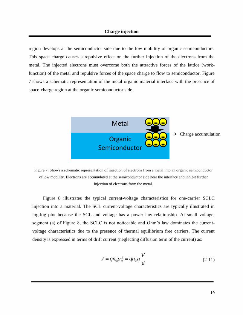
19
Charge injection
region develops at the semiconductor side due to the low mobility of organic semiconductors.
This space charge causes a repulsive effect on the further injection of the electrons from the
metal. The injected electrons must overcome both the attractive forces of the lattice (work-
function) of the metal and repulsive forces of the space charge to flow to semiconductor. Figure
7 shows a schematic representation of the metal-organic material interface with the presence of
space-charge region at the organic semiconductor side.
Figure 7: Shows a schematic representation of injection of electrons from a metal into an organic semiconductor
of low mobility. Electrons are accumulated at the semiconductor side near the interface and inhibit further
injection of electrons from the metal.
Figure 8 illustrates the typical current-voltage characteristics for one-carrier SCLC
injection into a material. The SCL current-voltage characteristics are typically illustrated in
log-log plot because the SCL and voltage has a power law relationship. At small voltage,
segment (a) of Figure 8, the SCLC is not noticeable and Ohm’s law dominates the current-
voltage characteristics due to the presence of thermal equilibrium free carriers. The current
density is expressed in terms of drift current (neglecting diffusion term of the current) as:
d
VqnqnJ 00 (2-11)
Organic Semiconductor
Metal
Charge accumulation

20
Charge injection
where 0
n is the thermal equilibrium free electron concentration (considering electron only), µ is
the charge carrier mobility, V is the applied voltage and d is the thickness of the specimen. As the
voltage increases, there is no significant departure from Ohm’s law until the average injected
excess free-electron concentration,njeectedi
n , becomes large enough to be noticeable. When
njeectedin becomes comparable to
0n , the space-charge-limited (SCL) mechanism becomes
noticeable and the current-voltage characteristics changes. Therefore, the onset of SCLC takes
place when the current-voltage characteristics begin to crossover from Ohm’s law to SCLC
regime. The voltage at which this crossover occurs is the crossover voltage, VΩ.
The total charge density into the semiconductor is given by
d qn d ρQ injectedinjectedinjected (2-12)
where injected
ρ is injected free charge concentration and injected
Q is total injected charge per unit
area. As stated above, the crossover voltage, VΩ, is the voltage when 0
nnnjeectedi
. Therefore,
d qnQinjected 0 (2-13)
If we consider organic semiconductor is sandwiched between two metals, then the total
charge per unit area, Q0, on one plate of the parallel-plate capacitor is proportional to the applied
voltage, V, across the capacitor, which can be written as:
dCV CQ and 000 (2-14)
21
Charge injection
where C0 is the capacitance per unit area of parallel-plate capacitor. From (2-12),
ΩΩinjected VdCVd qnQ 0 , by solving (2-13), VΩ can be written as
2
0 dqnVΩ (2-15)
where C is the capacitance of the device. By inserting a factor of 8/9, we get:
2
09
8 dqnVΩ (2-16)
As the voltage increases further, more electrons are injected from metal to
semiconductor. Due to the low mobility of organic semiconductors; these electrons are
accumulated near the metal-semiconductor interface and prevent further injection of electrons
(Figure 7). In simple words, the current is limited by its own space-charge, which in turn reduces
the electric field at the injecting electrode to zero. The screening due to these “space-charges”
produces non-linear current-voltage characteristics, segment (b) of Figure 8. The current density,
J, in the SCLC can be obtained by starting from the expression of the drift current and Gauss’s
law, we have:
ε
qn
dx
dqnJ
and (2-17)
where n0 = n + n injected. We can eliminate n , yielding:

22
Charge injection
dx
dJ
(2-18)
Integrating this expression from 0 to x, while assuming electric field to 0 at x = 0 one obtains:
xJ
Jx 2 or
2
2
(2-19)
Integrating once again over the thickness of the semiconductor from x = 0 to x = d, one finds:
2/3
2 dx
2/3d
0
dJ V
(2-20)
from which one obtains the expression for the SCLC as:
3
2
8
9
d
VJ
(2-21)
Equation (2-21) is known as the Mott-Gurney law for single-type of carriers and no traps
and Child’s law for solids [24]. This square law is the reason why the SCLC characteristics are
typically shown on log-log plot. Based on (2-21), the following two conditions should be
satisfied in a device that exhibits the SCLC phenomenon: (a) A plot of Jln versus Vln should
23
Charge injection
yield a region of slope equal to 2; (b) A plot of Jln versus d should yield a region of slope equal
to - 3. It is also important to note that equation (2-21) is for a trap-free case i.e. with the absence
of traps in the semiconductor. In the case of traps, the current density equation is modified by a
trap-limiting factor relating to the proportion of trapped charges )(t
p to free charges )( p by
3
2
8
9
d
VJ (2-22)
where
t pp
p θ
For a trap-free case, 0 t
p and therefore 1 ; with traps present, is always less than unity.
Throughout this thesis, equation (2-21) will be used to calculated the mobility of semiconductor
in the SCLC region by assuming 1.
With further increase in voltage, the injected charges are no more affected by space-
charges in the semiconductor since injected carriers become dominant process and the mobility
is assumed as band mobility, see segment (c) of Figure 8. We won’t explore this segment since it
is not the focus of this thesis. A good explanation of the basic SCLC theory can be found in [24]
by M. A. Lampert and P. Mark.

24
Charge injection
Figure 8: Current-voltage characteristics of Cu/CNCP/Al sample, Cu positively biased where CNCP stands for
conjugated non-conjugated alternating polymer. Segments (a), (b) and (c) corresponds to increasing voltage,
segment (d) corresponds to decreasing voltage, taken from [25].
6. SCLC mobility
As previously stated in Chapter 1, one of the methods of determining charge carrier mobilities
in organic semiconductor is by using SCLC technique. The mobility in the SCLC regime is
determined from the electrical characterization of a diode produced by sandwiching an organic
layer of interest between two metal electrodes. The choice of electrodes is made in such a way
that only quasi-unipolar (only positive or negative) charge carriers are injected into the active
layer.
d
VqpJ
0
VΩ
2
0
9
8 dqpV
SCLC
3
2
08
9
d
VJ
effr
Ohmic

25
Charge injection
Left picture of Figure 9 shows the energy scheme of a positive charge carrier-only device. On
one side, a metallic contact with a high work-function is chosen in such a way that the
difference between work-function of the metal and energy of the HOMO level of
semiconductor is almost negligible. On the opposite lying contact, a blocking/injection-limited
contact is formed between the work-function of the metal and the energy of the LUMO level of
semiconductor with a potential energy barrier, Φb. With positively-biased, the metal with
higher work-function can inject positive charge carriers in the HOMO of the semiconductor.
Due to the low mobility in disordered semiconductors, the desired carriers that are injected
from the electrical contacts begin to build up “space-charge”, as previously discussed. On the
other hand, the negatively-biased metal will have negligible injection of electrons due to the
high potential energy barrier, Φb, between work-function of the metal and the energy of the
LUMO level of semiconductor. The opposite is true if one fabricates an electron only device
shown in right picture of Figure 8. Therefore, to evaluate the carrier mobility using SCLC
method two requirements must be fulfilled: (a) Quasi-Ohmic contact at the metal-
semiconductor interface and (b) Unipolar charge injection.

26
Charge injection
Figure 9: Schematic figures of diodes with majority carriers as holes and electrons. In case of hole only device, only
the metal with the higher work-function can inject holes provided that the opposite lying contact is not a good
electron injecting contact. The opposite is true in the case of electron only device.
One of the fundamental differences between organic-on-metal and metal-on-organic interfaces is
that the former is usually formed by depositing the organic semiconductor by evaporation or by
spin coating on a metal that has been exposed to atmosphere and is therefore somewhat
contaminated: contaminants include hydrocarbons or residual solvent molecules that may be
present due to the processing conditions. This contaminant layer effectively passivates the metal
surface, and reduces the interaction between the organic molecules and metal, leading to an
energy band alignment that is close to the Schottky-Mott limit.
In contrast, metal-on-organic contacts are usually deposited by metal evaporation in
vacuum, where the presence of contaminants is greatly reduced. The stronger interaction
between the organic surface and the metal often induces a strong Fermi-level pinning and a large
LUMO
HOMO
LUMO
HOMO
Φb
Φb

27
Charge injection
interface dipole, causing the energy band alignment to depart from the vacuum level alignment
expected from the electronic structure of the isolated metal and semiconductor.
Data analysis is done by fitting J-V curves in the linear region (Ohmic region) and the
quadratic region (SCLC region), respectively. Generally, for Ohmic region, J is proportional to
V n, where n is the angular coefficient of the fitted curve and in the case of Ohmic region n 1.
For SCLC region, J is proportional to V n, where n 2. Also, the value of VΩ can be obtained by
the crossover point from Ohmic to SCLC regions. With the known value of VΩ and
semiconductor thickness and absolute permittivity one can calculate the value of 0
n using (2-
15). The knowledge of the value of 0
n can then be utilized to evaluate the charge carrier mobility in
the Ohmic region, which can be evaluated using (2-11). Similarly, the value of charge carrier
mobility in SCLC region can be evaluated by fitting of the SCLC region and utilizing (2-21).

28
3. Evaluation of transport properties in region-regular poly(3-
hexylthiophene) using SCLC method
1. Introduction
This chapter firstly gives a short introduction about regio-regular poly(3-hexylthiophene) (RR-
P3HT) and its properties. Secondly, the main motivation behind this project is discussed. Next,
fabrication, principle of operation and results based on the devices that are used to evaluate the
transport properties in RR-P3HT will be reviewed. Finally, conclusions based on the obtained
results and a glance at future work will be given.
2. Poly(3-hexylthiophene)
Poly(3-hexylthiophene) (P3HT) is one of the most studied semiconducting polymer due to its
high hole mobility, good solubility and processability [26]. It is stable both in doped and
undoped state. The 3-hexyl substituent in the thiophene ring can be incorporated into the
polymer chain with two different regio-regularities [27], shown in Figure 10 (A): head-to-tail
(HT) and head-to-head (HH). A regio-random P3HT consists of both HH and HT in a random
pattern while a regio-regular (RR) P3HT has only one kind of 3-hexylthiophene either HH or HT
(Figure 10 (B))
Figure 10: (A) Two different regio-regularities that can be incorporated into a polymer chain (B) The chemical
representation of regio-regular poly(3-hexylthiophene) (P3HT) [27].
29
Evaluation of transport properties in RR-P3HT
Upon casting onto thin films, RR-P3HT has great potential as an organic semiconductor in
electronics because of its strong tendency to self-assemble into crystallites with ordered
structures. This gives rise to positive charge carrier field-effect mobilties of the order
Vs/ cm 1.0 2 [28]. On the other hand, the regio-random P3HT has a twisted chain conformation
with poor packing and low crystallinity, resulting in positive charge carrier field-effect mobilities
of only Vs/ cm 10 24 [27]. Depending upon the processing conditions and regio-regularity of
the polymer, the polymer chains can be ordered in two different orientations, parallel or normal
to the substrates [28]. The mobilities had been found to be three orders of magnitude higher
when stacking direction is parallel to the direction of charge transport, thus demonstrating
fast and efficient interchain transport of the carriers. The morphology and charge transport of the
RR-P3HT has also been shown to depend on the molecular weight [29]. In addition, the choice
of solvents strongly influences the microscopic morphology of the film and thus its mobility
[26]. It has been established in the literature that the P3HT oxygen is known to form a charge
transfer complex resulting in p-doping of P3HT [30]. Furthermore, oxygen induced degradation
of P3HT is reported in decreased mobilities and increased trap densities [31].
3. Motivation
In the past, the charge carrier mobilites in P3HT has been evaluated using TOF method [32]. In
this report, they claimed that by using a high purity and chemical/structural regularity a relatively
high negative and positive charge carrier mobility in RR-P3HT can be obtained. To our
knowledge, till now SCLC method has only been employed to evaluate the positive charge
carrier mobility in P3HT [33]. The aim of this project is to evaluate both positive and negative
charge carrier mobility in RR-P3HT using SCLC method and then to compare it and analyze the
obtained results with the TOF results. Table 1 below compares the selected charge carrier
mobilities obtained by TOF and SCLC methods.
30
Evaluation of transport properties in RR-P3HT
Methods
Mobilities
)/Vscm ( 2
TOF [32] SCLC [33] SCLC (this
work)
h 4 -10 3
4 -5 - 10 10 ?
e 4 -10 5.1 _ ?
Table 1: Compares the selected positive charge carrier (µh) and negative charge carrier (µe) mobilities values
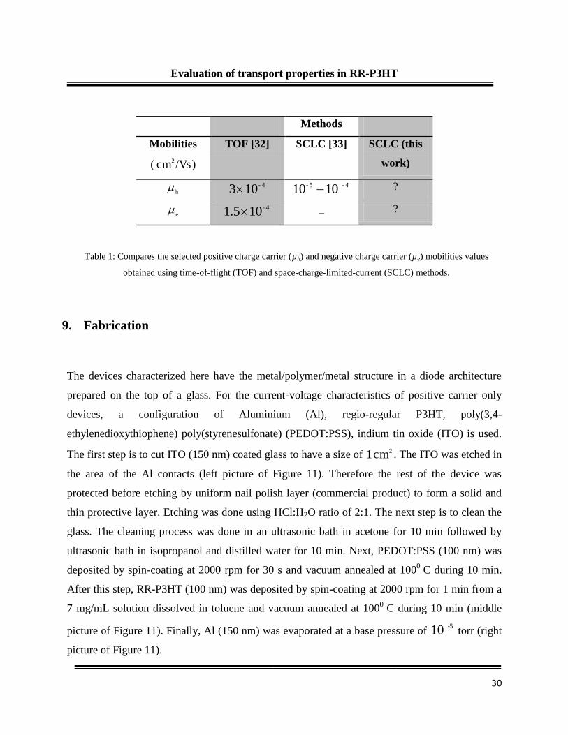
obtained using time-of-flight (TOF) and space-charge-limited-current (SCLC) methods.
9. Fabrication
The devices characterized here have the metal/polymer/metal structure in a diode architecture
prepared on the top of a glass. For the current-voltage characteristics of positive carrier only
devices, a configuration of Aluminium (Al), regio-regular P3HT, poly(3,4-
ethylenedioxythiophene) poly(styrenesulfonate) (PEDOT:PSS), indium tin oxide (ITO) is used.
The first step is to cut ITO (150 nm) coated glass to have a size of 2cm 1 . The ITO was etched in
the area of the Al contacts (left picture of Figure 11). Therefore the rest of the device was
protected before etching by uniform nail polish layer (commercial product) to form a solid and
thin protective layer. Etching was done using HCl:H2O ratio of 2:1. The next step is to clean the
glass. The cleaning process was done in an ultrasonic bath in acetone for 10 min followed by
ultrasonic bath in isopropanol and distilled water for 10 min. Next, PEDOT:PSS (100 nm) was
deposited by spin-coating at 2000 rpm for 30 s and vacuum annealed at 1000
C during 10 min.
After this step, RR-P3HT (100 nm) was deposited by spin-coating at 2000 rpm for 1 min from a
7 mg/mL solution dissolved in toluene and vacuum annealed at 1000
C during 10 min (middle
picture of Figure 11). Finally, Al (150 nm) was evaporated at a base pressure of -5 10 torr (right
picture of Figure 11).

31
Evaluation of transport properties in RR-P3HT
Figure 11: Left picture shows ITO glass substrate with etched ITO from the sides, middle picture shows the mixture
of spin-coated solutions of P3HT and PEDOT:PSS on top of ITO, right picture shows the evaporated Al electrodes
with as active area of 2cm 3.0 .
To evaluate the mobility of negative charge carriers a structure of Al/CsO/P3HT/CsO/Al was
used. In this work, after cleaning the glass, firstly, Al and caesium carbonate (Cs2CO3) were
evaporated at a base pressure of -5 10 torr. Evaporation of Cs2CO3 tends to deposit as a caesium
oxide (CsO) layer [34]. The CsO layer of 3 nm was deposited on top of the Al. Secondly, RR-
P3HT (100 nm) was spin coated with the procedure explained previously. Finally, Al and CsO
were deposited again by thermal sublimation on top of RR-P3HT. Al and CsO layers thicknesses
were monitored with the help of a quartz oscillator. P3HT and PEDOT:PSS thicknesses layers
were measured using DektaXT surface profiler. Both RR-P3HT and Cs2CO3 were purchased
from Sigma-Aldrich. In all the devices, the active area was defined to be 2cm 3.0 by using a
shadow mask.
Active area

32
Evaluation of transport properties in RR-P3HT
10. Principle of operation
Figure 12 shows the energy scheme of a positive charge carrier only device. As suggested
before, to evaluate the carrier mobility using SCLC method two requirements must be fulfilled:
(a) Quasi-Ohmic contact at the metal-semiconductor interface and (b) Unipolar charge
injection. To satisfying both the conditions, a PEDOT:PSS layer deposited on top of ITO is
chosen. PEDOT:PSS is chosen as a transport material for positive charge carrier’s transport
and is also known to give smooth and non-oxidizing interfaces [35]. PEDOT:PSS with a work-
function of 5.2 eV [36] tends to form an Ohmic contact for efficient hole injection in RR-
P3HT, which has a LUMO and HOMO energy levels of 3.0 eV and 5.0 eV, respectively [37,
38]. ITO with a work function of ~ 4.9 eV [39] is needed since it is easier to contact with
external wires as compared to PEDOT:PSS from our experimental point of view. The opposite
lying contact Al with a work-function of 4.3 eV [40] is chosen to form injection-limited
contact/barriers for the injection of both positive and negative charge carriers in P3HT,
respectively. These barriers are formed due to the position of the Fermi-level of Al with respect
to LUMO (HOMO) of P3HT. With ITO as positive biased, positive charge carriers (holes) can
be easily injected from PEDOT:PSS to HOMO of P3HT while Al as negatively biased cannot
inject negative charge carriers (electrons) due to the high energy barrier, Φb, between its Fermi
level and LUMO of P3HT.
33
Evaluation of transport properties in RR-P3HT
Figure 12: Schematic energy diagrams with respect to vacuum level for ITO (150 nm), PEDOT:PSS (100 nm),
region-regular P3HT (100 nm), Al (150 nm), a hole-only single-carrier devices. Holes are collected via PEDOT:PSS
of work-function eV 2.5 , by positively biased ITO electrode with work-function eV 9.4 . On the other hand,
negatively biased Al with a work-function eV 3.4 cannot inject electrons due to high energy barrier between its
Fermi-level and LUMO of P3HT.
Figure 13 shows the energy scheme of a negative only charge carrier device. The preparation
of efficient contacts for negative charge carrier injection is more problematic, since low work
function metals are highly reactive when exposed to oxygen and humidity. Recently, however,
an efficient negative charge carrier injection in Alq3, Tris-(8-hydroxyquinoline) aluminium,
was found by using a combination of Al/CsO [41]. Thermally evaporated CsO behaves as a
heavily n-doped semiconductor exhibiting high conductivity with an intrinsically low work
function. We use this strategy in our devices to inject negative charge carriers in the LUMO of
RR-P3HT (Figure 13). With one of the Al/CsO electrodes as negatively biased, electrons can
be easily injected to LUMO of P3HT while opposite lying Al/CsO electrode as positively
HOMO: 5.1 eV
LUMO: 3.2 eV
PEDOT:PSS: 5.2 eV
Al: 4.3 eV
electrons, e
-
holes, h+
ITO 4.9 eV
Hole transporting layer
Positive
electrode
Negative electrode
Active area
P3HT

34
Evaluation of transport properties in RR-P3HT
biased, cannot inject holes to HOMO of P3HT due to the due to the high energy barrier, Φb,
between its Fermi level and HOMO of P3HT.
Figure 13: Schematic energy diagrams for Al (150 nm), CsO (5 nm), region-regular P3HT (100 nm), CSO (5 nm),
Al (150 nm), an electron-only single-carrier device.
11. Results and Discussions
Current-voltage characteristics of the devices were measured using a Keithley 2602 source-
meter in air. The inset plot of Figure 14 shows the log current-voltage characteristics of
Al/P3HT/PEDOT:PSS/ITO diode with Al biased and PEDOT:PSS/ITO as grounded, as a hole
only device. With Al(+)/P3HT/PEDOT:PSS/ITO(-), respectively the diode current attains order
of magnitude in the range of mA at 3 V. On the other hand, with Al(-
)/P3HT/PEDOT:PSS/ITO(+), respectively the diode current attains order of magnitude in the
range of nA at 3 V. The rectification ratio, which is the ratio of currents measured at the same
absolute bias, at 3 V exceeds value of 106. This suggests that the
HOMO: 5.1 eV
LUMO: 3.2 eV
Al/CsO: 2.2
electrons, e-
holes, h+
Negative electrode
Active area
Positive electrode
Al/CsO: 2.2 eV
P3HT
35
Evaluation of transport properties in RR-P3HT
insertion of the PEDOT:PSS layer provides sufficient injection of positive charge carriers in
P3HT. Whereas, Al forms an injection-limited contact for the injection of both positive and
negative charge carriers in P3HT.
Further analysis of current-voltage characteristics of Al(+)/P3HT/PEDOT:PSS/ITO(-)
diode is done by plotting its characteristics in the log current-log voltage scale (main plot of
Figure 14).
Figure 13: Inset figure shows the current-voltage characteristics of Al/P3HT/PEDOT:PSS/ITO diode with Al biased.
Main figure shows the log-log plot of the inset figure with ITO and Al as positively and negatively biased,
Figure 14: Inset figure shows the current-voltage characteristics of Al/P3HT/PEDOT:PSS/ITO diode with Al biased
and PEDOT:PSS/ITO as grounded. Main figure shows the log-log plot of the inset figure with top contact Al/CsO
negatively biased and bottom contact Al/CsO positively biased, respectively. At low voltages (V < 1 V), an Ohmic
region is observed and at higher voltages (V > 1 V), SCLC region is observed.
0.1 1
10-4
10-3
10-2
-6 -4 -2 0 2 4 6
10-13
10-11
10-9
10-7
10-5
10-3
I (A
)
V (V)
(b)
(a)
I (A
)
V (V)
Ohmic
51. n
SCLC 272. n
VΩ

36
Evaluation of transport properties in RR-P3HT
It shows two distinct regions: At low voltage )V 1 (V , there is an Ohmic transport region
)( VI and at higher voltage )V 1 (V , SCLC region occurs corresponding to 2VI .
Substituting the values of VΩ = 0.9 V (from the main graph), q = 1.6 * 10 -19
C, d (P3HT)
= 100 nm, ε0 = 8.854 * 10 -12
Fm-1
, εr (P3HT) = 3 [42] in the equation (2-15),
2
098 dqpVΩ , one obtains the value of 0p = 1.68 × 10¹⁶
cm-3
. The value of 0p represents
the amount of thermally generated holes carriers in RR-P3HT at room temperature. Next step is
to calculate the Ohmic and SCLC hole mobilities, respectively. Ohmic mobility can be
calculated from (2-11), , 0 dVqpJ h which gives a value of µh (Ohmic) = 1.16 × 10⁻⁴
cm2/Vs and for SCLC region the hole mobility can be calculated using (2-21),
,89 32 dVJ which gives a value of µh (SCLC) = 1.35 × 10⁻⁴
cm2/Vs.
The inset plot of Figure 15 shows the current-voltage characteristics of
Al/CsO(top)/P3HT/Al/CsO(bottom) sandwich structure with top Al/CsO biased and bottom
Al/CsO grounded. It can be seen that the current-voltage characteristics is almost symmetric. It
means that the combination of Al/CsO on top of RR-P3HT has almost the same effect in both the
cases (i) when it is deposited over P3HT and (ii) when P3HT is deposited over it, despite the fact
that a native Al oxide layer is expected to be present before P3HT deposition on the bottom
electrode. The obtained rectification ratio at 3 V here is ~ 1. The main plot of Figure 15 shows
the log current-log voltage characteristics of Al/CsO(-)/P3HT/Al/CsO(+), respectively.

37
Evaluation of transport properties in RR-P3HT
0.1 1
10-8
10-7
10-6
-6 -4 -2 0 2 4 6
1E-8
1E-7
1E-6
I (A
)
V (V)
(b)
(a)
I (A
)
V (V)
Figure 15: Inset figure shows the current-voltage characteristics of Al/CsO (top)/P3HT/CsO/Al (bottom) diode with
top Al/CsO biased. Main figure shows the log-log plot of the inset figure with top contact Al/CsO negatively biased
and bottom contact Al/CsO positively biased, respectively. At low voltages (V < 1 V), an Ohmic region is observed
and at higher voltages (V > 1 V), SCLC region is observed.
Similarly to the previous results, the current-voltage characteristics of main plot show two
regions: At low voltage )V 1 (V , there is an Ohmic transport region . )( VI . At higher voltage
)V 1 (V , SCLC region occurs corresponding to 2VI . Substituting the values of VΩ = 1.8 V
(from the main graph), in the equation (2-15), 2
098 dqnVΩ , one gets the value of 0n =
3.36 × 10¹⁶
cm-3
. The value of 0n represents the amount of thermally generated negative carriers
Ohmic 31. n
SCLC
12. n
VΩ

38
Evaluation of transport properties in RR-P3HT
in RR-P3HT at room temperature. It is important to note that hat the value of 0n is of the same
order of magnitude of 0p . Using (2-11), dVqnJ h0 , the obtained value of µe (Ohmic) =
1.71 × 10⁻⁹
cm2/Vs and using (2-21), 32 89 dVJ , the obtained value of µe (SCLC) = 1.93 ×
10-9
cm2/Vs, respectively.
Table 2 compares the values of the mobility obtained here with the values measured by
TOF and SCLC methods in the literature. The values for positive charge carriers determined here
are in good agreement with those reported in literature [32, 33, 43, 44]. However, we have found
a substantially lower mobility of the negative charge carriers compared to the values obtained
using TOF method. In the article that used TOF method, they claimed to use a high purity and
chemical/structural regularity RR-P3HT. Also, they claimed that this is the first time such a
balanced and high positive and negative charge carriers mobilities are obtained for a conjugated
polymer. Although, the atmosphere in which the measurements were made is not identified.
Here, the thermally generated charge carriers concentration for both holes and electrons were of
the same order of magnitude, i.e. 0p = 0n = 1016
cm-3
, at room temperature. It means although the
thermally generated charge carrier concentrations in both carriers are of the same order of
magnitude, but based on mobility values the transport of positive charge carriers is much more
efficient than the negative charge carriers in RR-P3HT. The transport of negative charge carriers
in RR-P3HT could be hindered due to the combination of several factors including charge
transfer complex formed between RR-P3HT and oxygen due to the exposure of RR-P3HT during
the fabrication and electrical characterization process. This complex is known to remove the
negative charge carrier from P3HT, resulting in p-doping of P3HT [30]. Furthermore, oxygen
could induce degradation of P3HT and increase trap densities resulting in lower mobilities [31].
39
Evaluation of transport properties in RR-P3HT
12. Conclusions
An interesting conclusion can be made based on the obtained results is that when RR-P3HT is
exposed to oxygen and water moieties presence, the mobility of negative charge carriers is
affected decreasing by four orders of magnitude, but interestingly, the positive charge carrier’s
mobility remains almost unaffected. To our knowledge, this is the first time SCLC method has
been used to evaluate the negative charge carrier mobility in RR-P3HT.
Methods
Mobilities
)/Vscm ( 2
TOF [32] SCLC [33] SCLC (this
work)
h 4 -10 3
4 -5 - 10 10 4 -10 35.1
e 4 -10 5.1
_ 9 -10 93.1
Table 2: Compares obtained values of the positive (µh) and negative (µe) charge carrier mobilities using SCLC
method with the mobilities values obtained using time-of-flight (TOF) method.
13. Future work
To verify whether the variation of the space-charge limited current follows a 3 d law over the
thickness range of RR-P3HT, according to current density in the SCLC region 32 89 dVJ .
This could be done by varying the spinning speed to deposit RR-P3HT. This scaling states that
for a given mean electric field, the current density decreases inversely proportional to the third
power of the layer thickness of the organic semiconductor layer.
40
4. Controlled-Overflow-Transistor (COT)
1. Introduction
Today, we are living in the world of electronics and hence they immensely affect our daily life.
One of the main building block of all electronic components is the transistor. During the last 60
years, electronic industry was dominated by inorganic semiconductors such as Silicon (Si) and
Germanium (Ge). Despite its popularity, for some applications such as low cost, large area and
flexible electronics the use of inorganic semiconductors is not an ideal choice. This led to the
extensive research on various materials to find an appropriate alternative semiconductor for such
applications. Organic-based electronics provided this alternative due to its promising advantages
such as low-cost, simplification of production process, etc. To overcome the low mobility of
organic semiconductors, the application of organic transistors requiring high output currents
might be realized by the use of vertical devices. Here, charge carriers move through the device
perpendicularly to the substrate and thus have to travel less than a micron.
Many inorganic transistors exhibits a vertical geometry, therefore several attempts have
been made to transfer their structure to organic electronics. The modulation of current between
two separated electrodes by the use of a third electrode placed in between was first reported in
1926 when E. Lilienfeld patented the vacuum tube [45]. After more than 20 years, the bipolar
transistor was invented in Bell Laboraties [46], the vertical concept was applied successfully in
semiconductor technology.
This chapter firstly gives a short overview of some of the transistors based on vertical
architecture. It is followed by the main motivation behind the idea of Controlled-Overflow-
Transistor (COT). Next, materials, fabrication process, principle of operation and

41
Controlled-Overflow-Transistor
results obtained will be explained. Finally, conclusions based on the results COT will be
analyzed and a glance at future work will be given.
2. Transistors based on semiconducting materials
Metal-base transistor (MBT)
In 1932, Julius E. Lilienfeld applied for a patent on the amplification for a patent on the
amplification of current in a semiconductor-metal-semiconductor structure (Figure 16) [47].
Figure 16: Lilienfeld’s schematic drawing of the first current amplifier, (10), (11) marking the semiconductors and
(12) a metal layer [47].
The metal-base transistor (MBT) consists of two identically doped semiconductors layers
(emitter and collector) sandwiching a metal layer (base). The MBT is defined as hot-carrier
device since the electrons cross the middle electrode by ballistic transport. Thermalization, which
is an obvious limiting factor of the electron transfer through the base, depends upon the ratio of
the base layer thickness and the mean free path for electrons in the metal. Apart from crossing
the base metal, the electrons also have to overcome both emitter-base and base-collector
interfaces.

42
Controlled-Overflow-Transistor
The semiconductor materials are chosen in such a way that the energy barrier between emitter
and base (qϕBE) is higher than the energy barrier between base and collector (qϕBC) to have
efficient injection of charge carriers from emitter to collector (Figure 17) [48].
Figure 17: Energy band diagram of a MBT [48].
The current enhancement factor for common-emitter mode, β , is given by [21]
β = Ic/Ib (4-1)
Thus, β gives the ratio of amplified output current at the collector (Ic) to the base current (Ib).
The calculation is done similarly for common-base mode, here the common-base mode
enhancement factor α is obtained as the ratio of collector and emitter current:
α = Ic/Ie (4-2)
43
Controlled-Overflow-Transistor
In 2004, Hümmelgen et al. reported a n-type MBT using C60 and n type Si (n-Si) as emitter and
collector, respectively, and gold (Au) as a metal-base layer. For an operating voltage of 5 V, the
common-emitter current gain of 100 20 is calculated [49]. In 2008, Hümmelgen et al.
reported another n-type MBT in which Au was replaced by an organic conducting polymer P-
type sulfonated polyaniline (SPAN) as a metal-base layer. These devices were operated at low
operating voltages of 1 V to show common-emitter current gain equal to 8 [50].
Permeable-base transistor (PBT)
Like MBT, PBT is a majority carrier device. Electrons are transferred from emitter to collector
through pinholes in the base electrode instead the ballistic process known from the MBT. The
current is controlled by the barrier lowering in the pinholes. The size and distribution of holes
depends upon the materials used and on production. As current through openings and hot
electrons add up to the collector current, the problem of defining these two contributions arises.
The evidence of pinholes is provided by the measurement of the device in common-base mode.
If the base is continuous, it shields the emitter from the electric field which is generated by
application of collector voltage VCB and no change of emitter current Ie is observed. Thus, the
following equation is valid for a MBT with a continuous base:
0 CBe
VI (4-3)
For PBT, emitter current is affected by the application of collector voltage VCB
0 CBe
VI (4-4)
In 2009, Hümmelgen et al. reported P-type PBT using a combination of Al/V2O5/ 2,6-
diphenyl-indenofluorene layer as the emitter, a Ca/Al/Ca multilayer as the metal base, and p-Si
as collector [51]. They demonstrated a hybrid organic/inorganic PBT with a low-leakage current
in common-emitter mode and a highly reproducible common-emitter current gain of ~ 2
44
Controlled-Overflow-Transistor
independent of base current and collector voltage. In 2006, Horng et al. reported polymer space-
charge-limited transistor using a Al metal grid sandwiched between poly(3-hexylthiophene).
PEDOT:PSS and Al were used as emitter and collector, respectively [52]. Even though the name
of the transistor is different, but the principle of operation is similar to PBT. Here, the devices
were operated at a voltage of 3 V to achieve common-emitter current gain of 506.
3. Motivation
The previously discussed transistors i.e. MBT, PBT and polymer space-charge-limited transistors
showed promising results. However, one major drawback of these transistors is low emitter-
current gain. Table 3 compares the common-emitter gain values of the previously discussed
transistors. The aim of this work is to further enhance the performance of organic-based
transistor in vertical architecture by using a new family of transistors called as Controlled-
Overflow-Transistor (COT). The basic concept of COT is take advantage of low mobility in
conducting polymers. The idea is to form a blocking barrier (Schottky barrier) between
conducting organic semiconductor and an inorganic semiconductor and to use the space-charge
accumulation concept in the conducting organic semiconductor to control the charge overflow
through a Schottky barrier. This concept goes back to almost 50 years, in which a thin film
transistor operating under SCLC transport conditions was proposed using only a blocking contact
to isolate the gate electrode from the active layer. To our knowledge, this is the first time that
this idea has been implemented in a device.

45
Controlled-Overflow-Transistor
Transistors current gain references
Metal-base transistor 100 ± 20 [49]
Metal-base transistor 8 [50]
Permeable-base
transistor
2 [51]
Polymer space- charge-
limited transistor
506 [52]
Controlled-overflow
transistor
?
Table 3 Compares the common-emitter gain values of the metal-base, permeable-base and polymer space-
charge-limited transistors.
4. Self-doped sulfonated polyaniline (SPAN)
In COT, a self-doped p-type conducting polymer known as sulfonated polyaniline (SPAN) is
used as an active material. The following passages focuses on motivation, principle of operation
and chemical synthesis of SPAN.
Polyaniline
Polyanilines are a class of polymers where doping of the neutral form involves transfer of both
electrons and protons. It exists in three well defined oxidation states: leucoemeraldine,
emeraldine and pernigraniline. The leucomeraldine base is fully reduced (all amine nitrogens)
whereas the pernigraniline are fully oxidized (all imine nitrogens) and emeraldine form has an
imine/amine ratio of 5.0 [53]. Beginning from insulating leucomeraldine, electrically emeraldine

46
Controlled-Overflow-Transistor
can be obtained by oxidation process. Upon further oxidation, a fully oxidized pernigraniline can
be obtained (Figure 18).
Figure 18: Different bases of polyaniline formed by oxidative and protonic doping with HA as acid proton donor.
Undoped phase amine groups )( NH contains non-bonding (lone pairs) nitrogen orbitals while imine groups
)( N contains a mixture of lone pairs and -conjugated orbitals [54].
In addition these various oxidation states can be switched between doped salt and non-
doped base forms by protonation. Out of five forms of aniline, only the emeraldine salt is
conducting. Polyaniline is one of the most intensively studied conducting polymers due to its
unique properties such as wide range of electrical and optical tunable properties, good stability in
the presence of water and humidity, high conductivity, inexpensive monomer and ease of
preparation. It has been used for various applications such as transistors [55, 56], light emitting
diodes [57, 58], and rechargeable batteries [59-61]. However, limitations such as poor solubility

47
Controlled-Overflow-Transistor
in common solvents, pH dependent conductivity and electroactivity have limited its use in
industrial applications.
Self-doped polyaniline
To enhance the solubility of polyaniline in aqueous solution, a water soluble, self-doped,
conducting polyaniline derivative known as self-doped sulfonated polyaniline was discovered in
1990 by Yue and Epstein [62] and Dao et al. [63]. Initially, polianiline in its emarldine base form
is treated with polar sulfonotric acid groups. This will result in self-doped polymer, which has
the base formula of emeraldine base with sulfonated protonic groups )H3
(SO covalently bound
to its reduced and oxidized repeat groups (Figure 19)
HH
NH
3
NH
3
HH
NH
3
NH
3
HSO -
3
HSO -
3
x
Figure 19: Semiconducting state of sulfonated polaniline
The proton from the sulfonated group gets drawn to the imine groups, which has an immobile
electron system. This will induce bipolarons on the imine group sites (Figure 20).
HH
NH
3
NH
3
HH
NH
3
NH
3
-
3SO-
3SO
HH
HH
x
Figure 20: Formation of bipolarons

48
Controlled-Overflow-Transistor
Due to internal redox reaction, bipolarons are energetically unstable and lead to the formation of
two polarons with one unpaired electron per unit. The result is a half-filled and a potentially
metallic state where there is a positive charge in each repeated unit with its associated counterion
(Figure 21). Due to the electrostatic repulsion between the two positive charges, polarons will be
separated to yield a polaron lattice [64].
HH
NH
3
NH
3
HH
NH
3
NH
3
-
3SO-
3SOHH
HH
x
Figure 21: Conducting state of sulfonated polyaniline with no change in the number of electrons. The polarons
separates, which results in a polaron lattice [64].
Figures 19-21 showed the conversion of a polyaniline emeraldine base (semiconductor)
form to its emeraldine salt (conducting) form by protonation. The removal of protons will result
in the polar sulfonated groups (SO3-) with negative charges. The hydrophilic interactions
between the sulfonated groups and polar molecules of water enhance its solubility. Thus, the
sulfonate group not only improves water solubility but also acts as a charge balancing counterion
when the polymer is oxidized/reduced.
The conductivity of the SPAN depends upon the degree of sulfonation and the position
and nature of the side lateral group. Table 4 summarizes some of the results obtained by different
research groups. Even though the solubility of polyanilne is increased by the presence of
sulfonated groups along the polymer backbone, it also resulted in lowering of the conductivity.
The decrease in conductivity could be attributed to twisting of the phenyl rings relative to one
another and increased interchain separation (separation between two chains) due to increasing
sulfonate groups density causing lowering of π-orbital overlap [65].

49
Controlled-Overflow-Transistor
Structure Degree of Sulfonation
(%)
Conductivity (S/cm) References
50
75
100
0.1
1.0
10-2
-10-3
[66]
[67]
[68]
Table 4: The dependence of SPAN conductivity on the sulfonation degree.
Unlike polyaniline, sulfonated polaniline has much stronger temperature dependence of the
conductivity due to greater electron localization [68, 69, 70]. Unlike polyaniline, its conductivity
is independent of pH due to the presence of intrinsic acid on the polymer backbone. The pH
independence of conductivity up to 9 was reported [69].
SPAN preparation by chemical polymerization
In this research work, SPAN is prepared by copolymerization of monomers metanilic acid
(aminobenzenesulfonic acid containing sulfonic groups) and aniline with ammonium
perioxdisulfate as the oxidant. The extent of doping can be tuned through the choice of metanilic
acid/aniline ratios to vary the sulfonation degree by keeping the oxidant at a constant value. The
method used here is similar to the method used by Yang et al. [70].
N
H
SO3H
n

50
Controlled-Overflow-Transistor
The SPAN preparation was made by using two different solutions:
1) g 245.0 of metanilic acid was dissolved in mL 400 of deionized water, ultrasonicated for
10 min, followed by mixing μL 65 of aniline. The obtained solution was maintained at a
constant temperature )C10 ( 0 for one hour to stabilize aniline and to obtain homogenous
films;
2) Ammonium persulfate was used as an oxidant to form emeraldine base form of
polyaniline (Figure 18). A constant value of g 85.2 of (NH4)2S2O8 dissolved in mL 62 of
deionized water was used throughout the experiments. The obtained solution was kept
with the previous solution at a constant temperature )C10 ( 0 for one hour;
After one hour, the two solutions were mixed together to form SPAN. In time, the
solution color changes from a transparent color (semiconducting emeraldine base form) to blue
color (conducting emeralsine salt form). The whole process can be repeated to obtain different
degree of sulfonation by using different concentrations of metanilic acid with respect to aniline.
SPAN can be deposited on top of different materials provided that the interaction
between the surface of the material and the SPAN leads to deposition of homogeneous SPAN
film on top of the material. In this work, the SPAN, which was prepared using three times the
concentration of metanillic acid with respect to aniline ) 65 :g 0.245 3( L , was deposited on
top of <100> plane surface of n-Si with a doping level of -315 cm 10 (Figure 22). n-Si was
cleaned in a 1:1 of sulfuric and nitric acids (H2SO4:H2NO3) bath, followed by a 10 min ultrasonic
bath in distilled water. In the sequence, the samples were bathed in acetone, isopropanol and
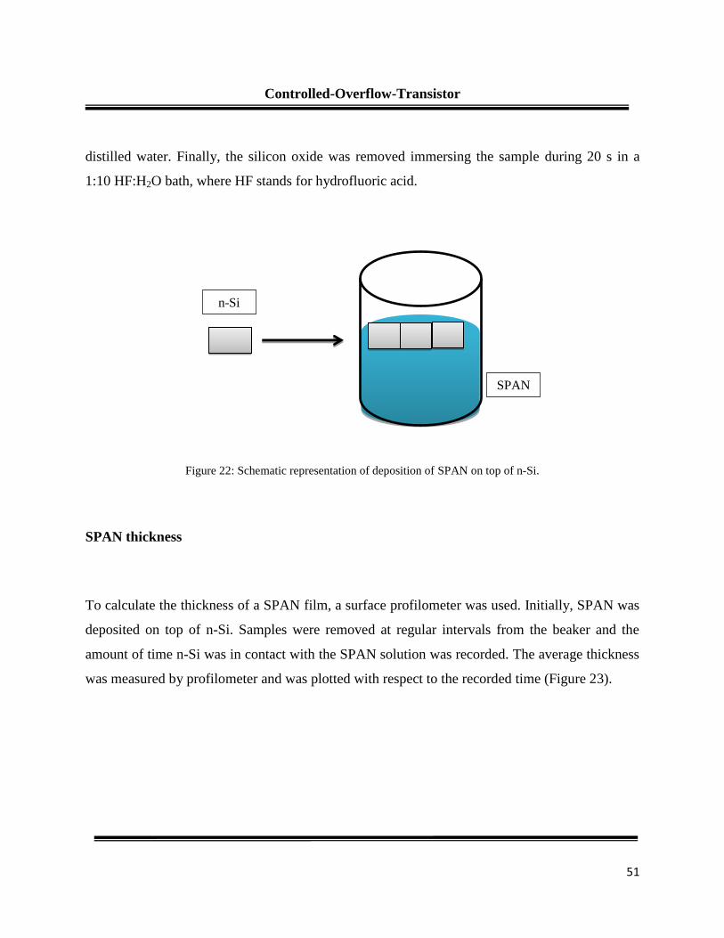
51
Controlled-Overflow-Transistor
distilled water. Finally, the silicon oxide was removed immersing the sample during 20 s in a
1:10 HF:H2O bath, where HF stands for hydrofluoric acid.
Figure 22: Schematic representation of deposition of SPAN on top of n-Si.
SPAN thickness
To calculate the thickness of a SPAN film, a surface profilometer was used. Initially, SPAN was
deposited on top of n-Si. Samples were removed at regular intervals from the beaker and the
amount of time n-Si was in contact with the SPAN solution was recorded. The average thickness
was measured by profilometer and was plotted with respect to the recorded time (Figure 23).
SPAN
n-Si

52
Controlled-Overflow-Transistor
Figure 23: SPAN thickness as a function of the amount of time (in hours) n-Si was in contact in the SPAN solution.
SPAN roughness
It was observed that the SPAN film layer is amorphous and the growth rate as well as its average
roughness )( aR increases with increase in concentration of metanillic acid. This phenomenon
was observed by using AFM images of the SPAN layer. The samples were prepared using the
following concentrations:
53
Controlled-Overflow-Transistor
1:1 ratio of metanillic acid and aniline;
3:1 ratio of metanillic acid and aniline;
5:1 rato of metanillic acid and aniline;
7:1 ratio of metanillic acid and aniline
After preparation with different concentrations, samples of n-Si were removed from the SPAN
solution on the third day to make a consistent comparison. AFM images showed the increase of
nm 19 aR for 1:1 ratio to nm 42 aR for 7:1 ratio (Figure 24). Even though, the difference of
aR is very small after 3 days, but with time the difference could be large enough to make an
impact on the deposition process of SPAN on top of various materials Thickness dependence of
surface morphology and its influence on the charge carrier mobility in organic semiconductor
has been studied briefly before in [71].
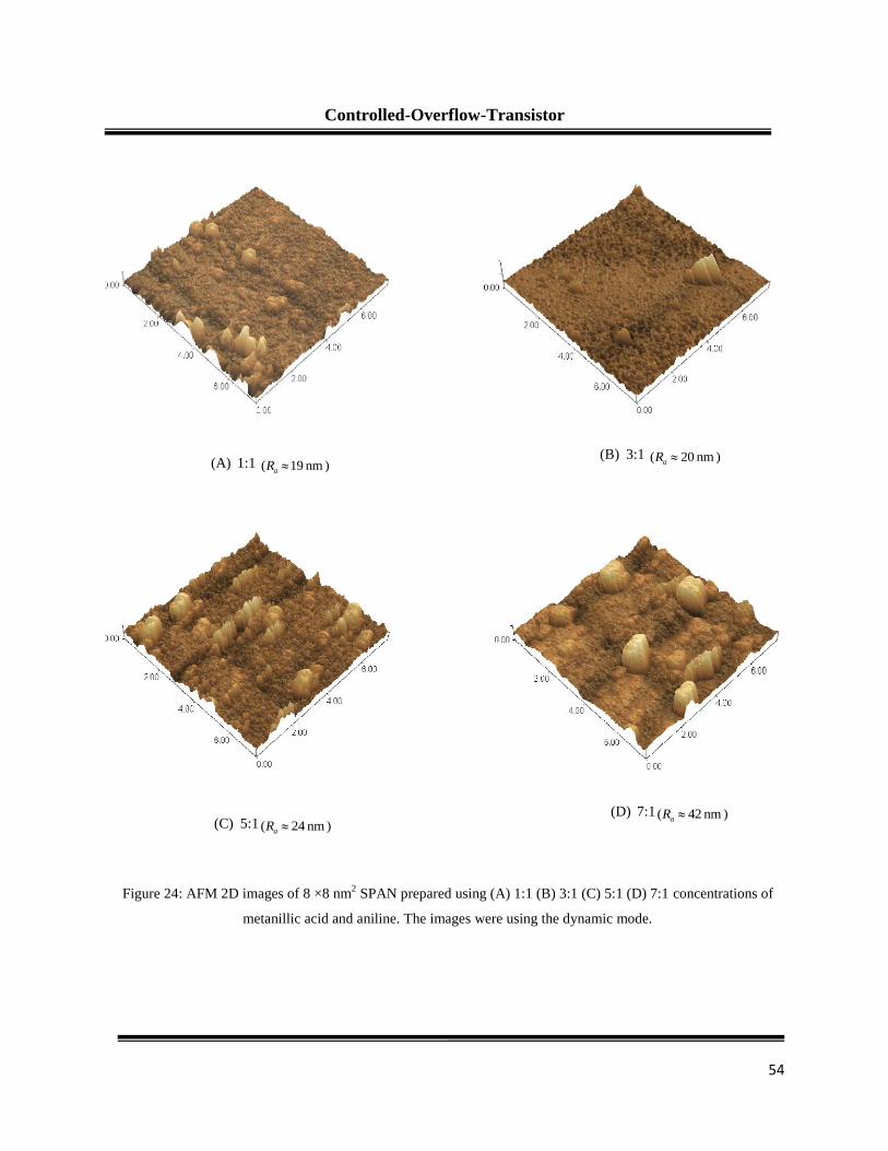
54
Controlled-Overflow-Transistor
Figure 24: AFM 2D images of 8 ×8 nm2 SPAN prepared using (A) 1:1 (B) 3:1 (C) 5:1 (D) 7:1 concentrations of
metanillic acid and aniline. The images were using the dynamic mode.
(A) 1:1 ) nm 19 ( aR (B) 3:1 ) nm 20 ( aR
(C) 5:1 ) nm 24 ( aR (D) 7:1 ) nm 42 ( aR

55
Controlled-Overflow-Transistor
SPAN sheet resistance
SPAN sheet resistance was performed using four-point probe method by depositing SPAN on
top of a glass (Figure 25). The probe configuration used here is the linear four point probe array.
In this method, two probes carry the current and other two probes measure the voltage by using a
high impedance voltmeter. Since the high impedance draws very little current the effects
introduced by probe resistance, probe contact resistance and spreading resistance is negligible.
The voltmeter reading is equal to the voltage drop across the SPAN sheet. The sheet resistance
SR can be calculated by
RS ∝ V/I
where V is the voltage reading from voltmeter and I is the current carried by two-current
carrying probes. The calculated sheet resistance of SPAN was found to be in the range of.1-6
MΩ/ . For more detailed information on sheet resistance refer to chapter 4 of [72].
Figure 25: Schematic figure of a linear four-point probe technique used to measure SPAN sheet resistance on top of
a glass.
(4.5)

56
Controlled-Overflow-Transistor
How can a conducting polymer have such a high sheet resistance? To understand this one has to
look beyond Ohm’s law. It is entirely possible that the charge carrier paths in the SPAN film are
hindered due to the presence of impurity and defect scattering. Usually, scattering of carrier
decreases their mean-free path, which ultimately could lead to high S
R . Additionally, as
discussed previously, the presence of substituents can also decrease the overlap of π-orbital
which reduces the delocalization of π-electrons. The reasons mentioned are very crude as at this
point there is no clear explanation for the high sheet resistance of SPAN.
To conclude, SPAN has the following properties:
It is a p-type conducting polymer;
Its conductivity as well as its roughness depends upon the degree of sulfonation used in
preparing SPAN.
It has a high sheet resistance;
5. COT fabrication
To begin with, a 3 -15 cm 10 phosphorus doped n-type <100> n-Si is used as a substrate. It was
cleaned using sulfuric and nitric acids (50:50), acetone and isopropanol were used to remove the
metallic and organic containments. After each bath, the substrate was rinsed in distilled water.
The oxide layer (insulating layer) present on top of the substrate was removed by dipping it into
a solution of 48 % hydrofluoric acid (HF) acid diluted in distilled water (1:10) for 20 seconds.
The absence of oxide layer makes the surface of the substrate hydrophobic.

57
Controlled-Overflow-Transistor
The next step is to deposit SPAN with thickness t by chemical polymerization on top of the
substrate. A 3:1 ratio of metanillic acid and aniline was used in this work. The n-Si substrates
were removed from the SPAN solution once it attained a desired thickness according to the
previously obtained recorded time. After drying the films, Al contacts (150 nm) were evaporated
as source (S) and control (CT) terminals at a base pressure of torr10 5 6 . This process was
monitored using quartz oscillator. The two contacts were separated by a channel length .L In
this configuration, the channel length L is kept always larger than the SPAN thickness t .
Finally, a Al:Ga eutectic alloy was applied on the Si backside to provide an ohmic contact
(interconnected materials have low resistivity) acting as drain (D), see Figure 26 [73].
Figure 26: Schematic representation of a controlled-channel-overflow transistor using Al contacts as source and
control-terminals and drain as n- Si [73].
It is important to note that both source and control terminals are made from the same material
and their role is determined by the electric potential applied to the terminals. As a result, if
desired, the roles of source and control-terminals can be interchanged. Compared to the vertical
organic field-effect transistors (VOFETs), the structure of this device is much simpler since it
does not involve an insulating layer. The elimination of this layer might reduce the production
cost, time and also remove the risk of high leakage current through the insulator, which is
58
Controlled-Overflow-Transistor
encountered in VOFET. Despite the absence of the insulator, the structure of this transistor is
similar to an OFET, though the principle of operation is completely different.
6. Junction characteristics
As discussed previously, to have a breeding ground for space-charge transport in a conducting
polymer, it is essential to have an ohmic or quasi-ohmic contact between the injecting metal
electrode and the semiconductor. Therefore, it is important to begin by studying the density of
states of SPAN. An analysis using density functional theory (DFT) simulation of an isolated
molecule of SPAN at the B3LYP/3-21G(d) level of theory was done in [73]. It was found that
the LUMO and HOMO of SPAN tetramer are around eV 7.3 and eV 12.5 , respectively. Note that
even though these values are obtained for SPAN tetramer, but we will apply these values of
HOMO and LUMO to the SPAN film. The obtained value of the HOMO value of SPAN matches
the value obtained previously with the ionization potential of SPAN [74]. In the latter case, the
HOMO value of SPAN was estimated by the Schottky energy barrier at the SPAN/n-Si interface,
which by using Richarson-Schottky equation was found to be eV 0.1 to the silicon electron
affinity ) 1.4( eV [23]. It was also found by using DFT simulation that the density of states has
a group of four unoccupied electronic states very close to 3.65 eV, see Figure 27 [73]. These
unoccupied states can be filled by the electron injection from a low work function metal.

59
Controlled-Overflow-Transistor
Figure 27: Density of electronic states of SPAN tetramer as a function of the energy with respect to the vacuum
level. The average position of LUMO is at 3.7 eV below the vacuum level. HOMO is approximately at 5.12 eV.
Inset: ground state geometry of the SPAN tetramer [73].
We used Al and Au with work-functions of eV 3.4 and eV 1.5 [40, 75] to verify the presence of
the low energy tail of the empty states distribution in the SPAN. To confirm the above
assumption practically, we used a diode structure of Al(-)/SPAN/n-Si/Al(+) and Au(-)/SPAN/n-
Si/Al(+) devices. Using the current-voltage characteristics, the idea behind these devices is to
fabricate an electron-only device and observe which metal electrode is able to better transport
electrons giving higher currents in SPAN. Figure 28 compares the current-voltage characteristics
of both devices [73]. It is clear that the current values in the case of Al are much higher than the
Au. These results confirm that LUMO energy levels of SPAN are located around the work
function of Al. Ohmic injection at the SPAN/ Al interface was reported in [76]. However, in the
latter case, SPAN was prepared by electrochemical polymerization instead of chemical
polymerization. It is important to note that the electrons of Al, when injected into the SPAN, will
become minority carriers since SPAN is a p-type conducting polymer. All the devices were
3.7 eV
5.12 eV
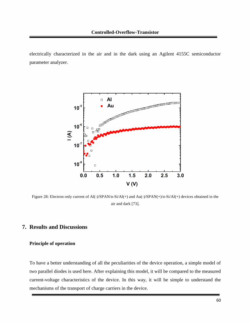
60
Controlled-Overflow-Transistor
electrically characterized in the air and in the dark using an Agilent 4155C semiconductor
parameter analyzer.
Figure 28: Electron only current of Al(-)/SPAN/n-Si/Al(+) and Au(-)/SPAN(+)/n-Si/Al(+) devices obtained in the
air and dark [73].
7. Results and Discussions
Principle of operation
To have a better understanding of all the peculiarities of the device operation, a simple model of
two parallel diodes is used here. After explaining this model, it will be compared to the measured
current-voltage characteristics of the device. In this way, it will be simple to understand the
mechanisms of the transport of charge carriers in the device.

61
Controlled-Overflow-Transistor
This device can be pictured as a parallel association of two reverse biased Schottky junctions
between (1) control-terminal and drain terminals (CT-D) and (2) source and drain terminals (S-
D). These two junctions are separated by the resistance of the SPAN layer (Figure 29). The
current along the SPAN film between S and CT is CTS
I
, the current between CT and D diode
is DCT
I
and the current between S and D diode is DS
I
.
Figure 29: Schematic representation of a model with two parallel Schottky diodes between CT-D and S-D with its
respective currents.
Initially, when there is no electrical potential applied between the control-terminal and the source
terminals V) V SCT 0 ( , it is expected that the currents 0 DSDCT
II , since the contacts
have the same area and therefore as a result 0 2
DSDSDCTD
IIII . If we consider
two diode junctions (S-D and CT-D) as independent and non-interacting, then the application
SPAN
CT S
D
CT S
CTSI
D
DSI
DCTI
S CT V -
CT D V - S D V -
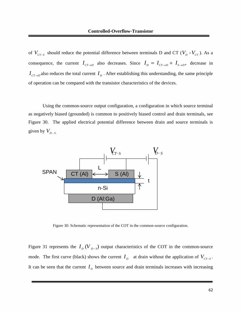
62
Controlled-Overflow-Transistor
of SCT
V
should reduce the potential difference between terminals D and CT (CTD
VV - ). As a
consequence, the current DCT
I
also decreases. Since , DSDCTD
III
decrease in
DCTI
also reduces the total current
DI . After establishing this understanding, the same principle
of operation can be compared with the transistor characteristics of the devices.
Using the common-source output configuration, a configuration in which source terminal
as negatively biased (grounded) is common to positively biased control and drain terminals, see
Figure 30. The applied electrical potential difference between drain and source terminals is
given by . SD
V
Figure 30: Schematic representation of the COT in the common-source configuration.
Figure 31 represents the )( SDD
VI
output characteristics of the COT in the common-source
mode. The first curve (black) shows the current D
I at drain without the application of SCT
V
.
It can be seen that the current D
I between source and drain terminals increases with increasing
n-Si
SPAN L
t
CT (Al) S (Al)
D (Al:Ga)
S CT V - S D V -
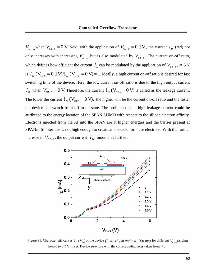
63
Controlled-Overflow-Transistor
. SDV
when V. 0
SCTV Next, with the application of V 0.1
SCTV , the current
DI (red) not
only increases with increasing , SD
V
but is also modulated by SCT
V
. The current on-off ratio,
which defines how efficient the current D
I can be modulated by the application of SCT
V
, at 5 V
is V) 0 (V V)/I 0.1 (V CT-SDCT-SD
I ≈ 1. Ideally, a high current on-off ratio is desired for fast
switching time of the device. Here, the low current on-off ratio is due to the high output current
DI when V. 0
SCTV Therefore, the current V) 0 (V I
CT-SDis called as the leakage current.
The lower the current V), 0 (V I CT-SD
the higher will be the current on-off ratio and the faster
the device can switch from off-to-on state. The problem of this high leakage current could be
attributed to the energy location of the SPAN LUMO with respect to the silicon electron affinity.
Electrons injected from the Al into the SPAN are at higher energies and the barrier present at
SPAN/n-Si interface is not high enough to create an obstacle for these electrons. With the further
increase in SCT
V
, the output current D
I modulates further.
Figure 31: Characteristic curves ) (D
VID
of the device nm) m and t (L 20045 for different S-CT
V ranging
from 0 to 0.5 V. Inset: Device structure with the corresponding axes taken from [73].
VD-S (V)
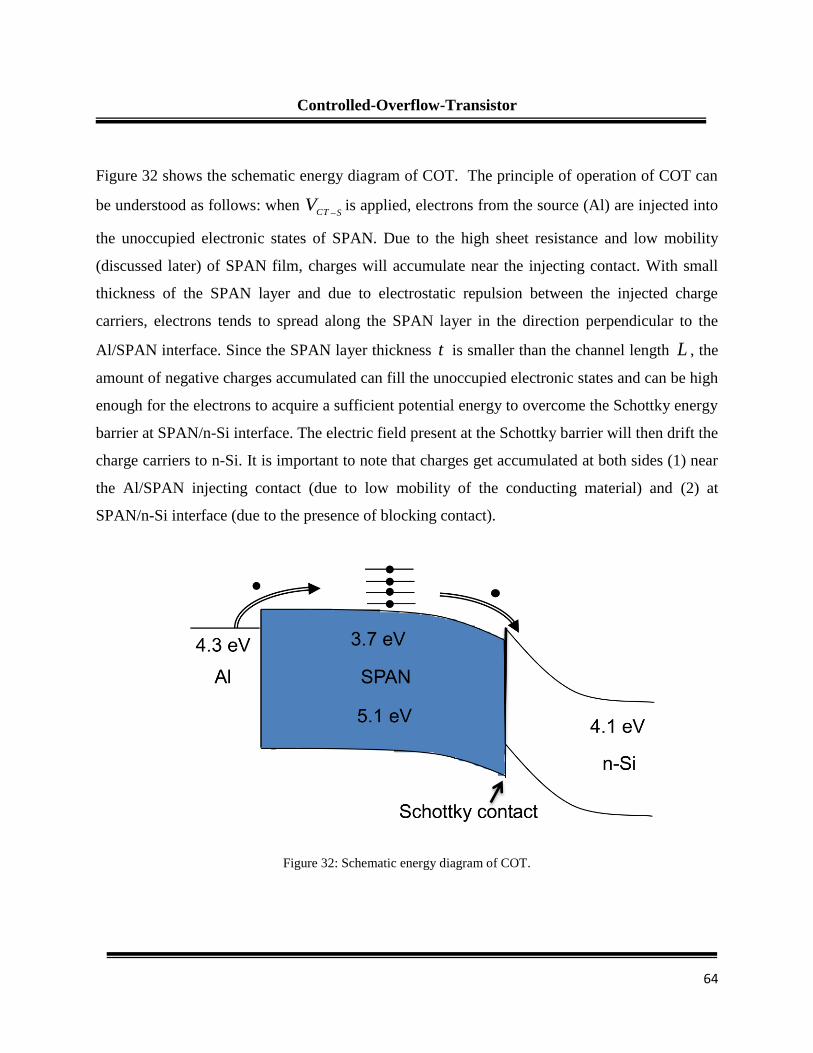
64
Controlled-Overflow-Transistor
Figure 32 shows the schematic energy diagram of COT. The principle of operation of COT can
be understood as follows: when SCT
V
is applied, electrons from the source (Al) are injected into
the unoccupied electronic states of SPAN. Due to the high sheet resistance and low mobility
(discussed later) of SPAN film, charges will accumulate near the injecting contact. With small
thickness of the SPAN layer and due to electrostatic repulsion between the injected charge
carriers, electrons tends to spread along the SPAN layer in the direction perpendicular to the
Al/SPAN interface. Since the SPAN layer thickness t is smaller than the channel length L , the
amount of negative charges accumulated can fill the unoccupied electronic states and can be high
enough for the electrons to acquire a sufficient potential energy to overcome the Schottky energy
barrier at SPAN/n-Si interface. The electric field present at the Schottky barrier will then drift the
charge carriers to n-Si. It is important to note that charges get accumulated at both sides (1) near
the Al/SPAN injecting contact (due to low mobility of the conducting material) and (2) at
SPAN/n-Si interface (due to the presence of blocking contact).
Figure 32: Schematic energy diagram of COT.

65
Controlled-Overflow-Transistor
Contrary to the diode model, it is clear that the current D
I increases with SCT
V
. There must be
some additional effect which is increasing the current DS
I
larger than the reduction of DCT
I
.
Under these circumstances, both diodes show different current-voltage characteristics. The gain
comes from the fact that the current along the SPAN layer between source and control-terminals
CTS
I
is small, due to the high sheet resistance of SPAN, than the DS
I
so that
1 )/ ( CTSDSDCT
III . This common-source current gain )( can be defined by the
relationship:
)( CTD
dIdI
To understand the physics behind the increase of DS
I
under the application of a
positive SCT
V
, current-voltage characteristics in Figure 30 will be characterized into two
regimes namely SCLC and thermionic based on lower and higher electric field strengths.
SCLC regime
With the observation of a quasi-Ohmic contact at Al/SPAN interface, charge carries are injected
upon the application of SD
V
and accumulated near the injecting contact. This charge
accumulation gives rise to SCLC phenomenon along the SPAN layer, which further limits the
charge carrier transport between Al electrodes and n-Si. Figure 33 shows the current-voltage
characteristics in the log-log scale with the angular coefficient of 2 (dark line). For
1 S - D
VV
SCT, the current
DI has a power-law dependence on
SDV
and almost does not
depend on SCT
V
. The SD D VI characteristics in this regime can be described by Mott-
(4.6)

66
Controlled-Overflow-Transistor
Gurney’s law and mobility can be calculated by using the equation (2.21). Using the value of
SPAN thickness of t = 200 nm and fitting to the experimental data, the calculated mobility value
of electrons in the SPAN is 1 -12-7 S cm 10 2.2 V . This results show that not only SPAN has
high sheet resistance but also has low electron mobility. Note that in this voltage range,
D
I drops with increase in SCT
V
for a fixed S - D
V . This is due to the fact that DCT
I
decreases
with increasingSCT
V
, while DS
I
remains constant.
Figure 33: log-log plot of the )(D
VID
data of Figure 30 for different S CT
V
in the range V 1 D
V . The continuous
line is a power-law fit to the experimental data with exponent 2 [73].
Thermionic regime
With increase in D
V , the quasi-Fermi level for electrons at the blocking contact of SPAN/n-Si
interface rises due to charge accumulation so that the effective barrier height at Schottky diode is
VD-S (V)

67
Controlled-Overflow-Transistor
lowered due to the Schottky effect. As a result, a significant density of electrons can overcome
the blocking contact and reach the silicon layer. This will drain the accumulation of carrier at the
Al/SPAN interface. Thus, the DD
VI characteristics reach a new regime where the current flow
is limited by the thermionic injection over the reduced barrier at SPAN/n-Si interface.
We performed an analysis of D
I dependence on SCT
V
in the range of V 1 S - DV to demonstrate
the presence of Schottky effect and the reason behind the increase of DS
I
upon the application
of SCT
V
. Figure 33 shows the 2/1
DV ][ ln
DI (main plot) of the experimental data of Figure 30
for V 0 SCT
V and 0.5 V. Starting with analyzing the measured curves without the application
of SCT
V
(open circles). The linear curve fits the experimental data with an angular coefficient of
1.53. This value was compared to the theoretically calculated value of angular coefficient by
using (2-7) 2/14
SBq where
S is the electrical permittivity of n-Si. In the thermionic
regime, one can write SDSSDCTDCTDSD
qqIIII 4exp 4exp 0
where
DCT and
DS are the electric fields in the n-Si at S-D and CT-D diodes, respectively. These
fields are related to the respective fields in the polymer layer by the ratio between SPAN and n-
Si dielectric constants or
pol
sDS DS
)(
poland
pol
sDCT DCT
)(
pol (4.7)
0I is the drain current at the transition between SCLC regime and thermionic regime each
crossing Schottky junction. If V, 0 SCT
V the electric field at the S-D and CT-D diodes is
equal. Assuming tpolpol
DSDCT/V
S-D
and using (4-7), we find that 1/2
Dt00Vexp2I
DI
when V 0 SCT
V , where coefficient t
is given by
2
s tKT)( 4 tq
pol (4.8)

68
Controlled-Overflow-Transistor
Taking t = 200 nm, K 300 T and 3.8 ,30s0
pol
in (4-8), one gets t
= 1.606. This
small difference between the values of the angular coefficient obtained by the fitting in Figure 34
and the value calculated using (4.8) might be due to fact local electric field at the SPAN/n-Si
interface is different than the average value of electric field, estimated while calculating, along
the SPAN layer. This result suggested that the Schottky effect is the mechanism behind increase
of D
I with . SD
V
The above theoretically calculated value of angular coefficient was
performed by Koehler et al. [73].
Figure 34: ln I versus 1/2V plot of Figure 42 for . and VSCT
V50V0
in the range V.1 S -
DV The continuous
lines are straight lines fitting to the experimental data. Inset: The linear coefficient of the continuous lines in the
ln I versus 1/2V plot [73].
Figure 34 shows the dependence of D
I with the application of SCT
V
. One can see that curve
with V 0.5 SCT
V is a straight line parallel to the line measured with V 0 SCT
V in the

69
Controlled-Overflow-Transistor
2/1V ][ lnD-SD
I plot. Similarly the curves for other values of SCT
V
(0.1, 0.2, 0.3, and 0.4 V)
measured formed a family of straight lines parallel to the line obtained with V 0 SCT
V (those
curves are not shown in Figure 33 to preserve the plot’s clarity). The inset to Figure 33 shows the
linear coefficients of the straight lines (with angular coefficient equals to 1.53) that fit the
experimental data for different SCT
V
in the 2/1V ][ lnD-SD
I plot. The results in Figure 34 suggest
that the variation of ID upon the application of SCT
V
comes from an additional Schottky effect
across the SPAN/Si diode due to the extra electric field created by the control voltage.
In the thermionic regime, S - D
V is considerably higher than SCT
V
. We thus model the
dependence of ID on SCT
V
by assuming that the current between the source and drain is
enhanced by an additional component along the y-direction of the electric field (ξ SCT ) created
by the application of SCT
V
. Figure 35 shows the distribution of electric field lines in COT by the
application of SCT
V
and SD
V
. The distribution of field lines (black) of the electric field created
by SCT
V
is not only in the direction of CT and S electrodes (responsible forSCT
I
) in the x -
direction, but also connecting the metallic source to n-Si in the y – direction. This additional
component of SCT
V
in the y-direction is the reason behind the increase of DS
I
upon the
application of SCT
V
. The electric field lines (red) created by the SD
V
is in y- direction.
Figure 35: Schematic figure of electric field lines in the colors blue and black produced by the voltages VCT-S and
VD-S, respectively. The additional effect in COT comes from the distribution of electric field lines produced by VCT-S
in x as well as y-direction.
ξ
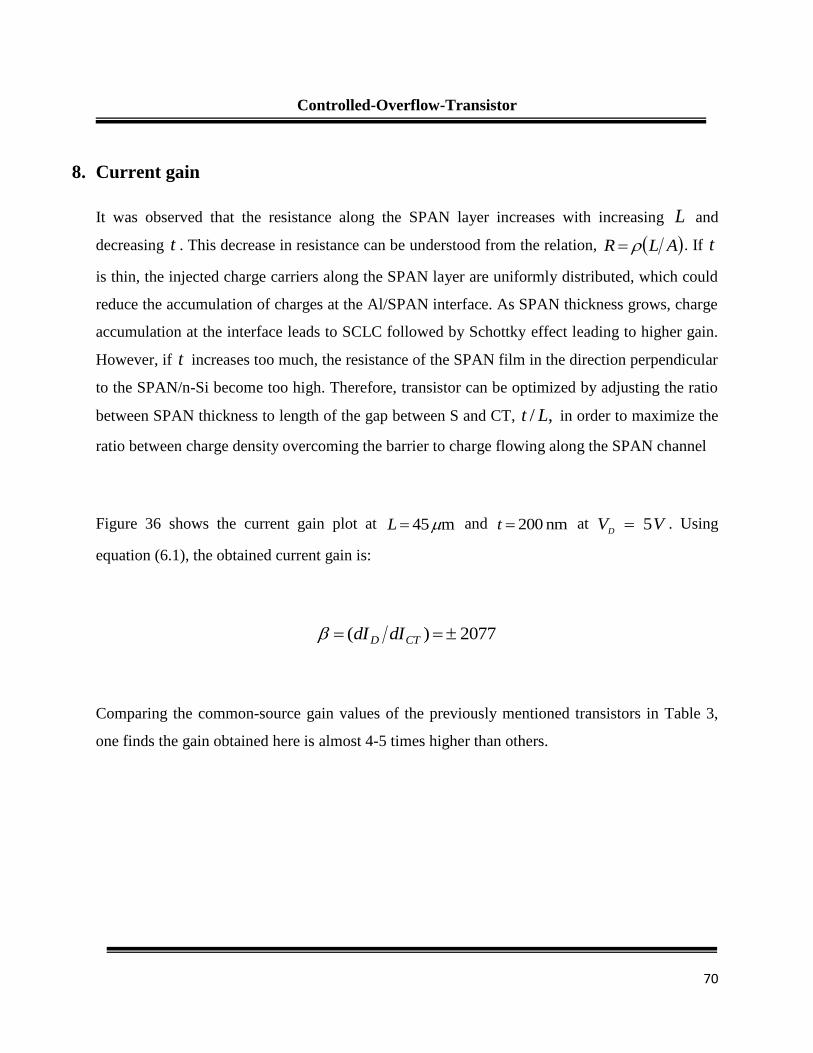
70
Controlled-Overflow-Transistor
8. Current gain
It was observed that the resistance along the SPAN layer increases with increasing L and
decreasing t . This decrease in resistance can be understood from the relation, ALR . If t
is thin, the injected charge carriers along the SPAN layer are uniformly distributed, which could
reduce the accumulation of charges at the Al/SPAN interface. As SPAN thickness grows, charge
accumulation at the interface leads to SCLC followed by Schottky effect leading to higher gain.
However, if t increases too much, the resistance of the SPAN film in the direction perpendicular
to the SPAN/n-Si become too high. Therefore, transistor can be optimized by adjusting the ratio
between SPAN thickness to length of the gap between S and CT, ,/ Lt in order to maximize the
ratio between charge density overcoming the barrier to charge flowing along the SPAN channel
Figure 36 shows the current gain plot at m 45 L and nm 200 t at V VD
5 . Using
equation (6.1), the obtained current gain is:
2077 )( CTD dIdI
Comparing the common-source gain values of the previously mentioned transistors in Table 3,
one finds the gain obtained here is almost 4-5 times higher than others.

71
Controlled-Overflow-Transistor
Figure 36: )(D
VID
device characteristic for nm) m and t (L 20045 at V VD
5 to calculate the
2077 [73].
Table 5 below compares the common-emitter gain obtained with different L and t devices at
V VD
5 . Conditions where gain was not observed are indicated by "."

72
Controlled-Overflow-Transistor
Till this part, all the previously stated experiments results were published in [73]. Unfortunately,
we could not further investigate the device because the aniline that was used in preparing the
SPAN was finished. Newly synthesized aniline was used to repeat the experiments, but the
devices could not reproduce the results.
9. Conclusions
Advantages
Low production cost and less time consuming in fabrication since the deposition of
insulating layer is eliminated;
This transistor produces a high common-source output current in the order of mA with
very low operating voltage;
Shows high current gain depending upon the thickness of SPAN and the distance
between two Al electrodes. Table 6 below compares some of the current gains obtained
for different architectures of transistors
Transistors current gain references
Metal-base transistor 100 ± 20 [49]
Metal-base transistor 8 [50]
Permeable-base
transistor
2 [51]
Polymer space- charge-
limited transistor
506 [52]
Controlled-overflow
transistor
± 2077
Table 6: Comparisons of current gain achieved with different configurations of the transistors.
73
Controlled-Overflow-Transistor
The transistor structure used here can also be applied to other organic and inorganic
materials;
Drawbacks
One big challenge of this device is that it suffers from a high leakage current;
Device performance depends upon the properties the chemical nature of SPAN. This is a
difficult to control since the SPAN properties depends upon many factors like the
monomers used and the preparation method;
10. Future work
To repeat the previous results with the application of new synthesized aniline and then to
further enhance the performance of the device;
Leakage current may be controlled by forming a thin silicon oxide or by use different
combination of materials at the SPAN/n-type Si interface to form an effective injection
limiting barrier;
To test the device with magnetic-field application;

i
References
[1] S. Frenkel, Plastic: A Toxic Love Story. Houghton MIffin Harcourt, 2011.
[2] H. P. Kallman, M. Pope and P. Magnanate, Electroluminescence in Organic Crystals,
Journal of Chemical Physics, 1963. 38(8) p. 2042-2043.
[3] H. Shirakawa, E. J. Louis, A. G. MacDiarmid, C.K. Chiang, and A. J. Heeger, Synthesis of
electrically conducting organic polymers – halogen derivatives of polyacetylene, (CH)x,
Journal of the Chemical Society-Chemical Communications, 1977. (16) p.578-580.
[4] R. W. Gundlach, Xerography from the beginning, Journal of Electrostatics, 1989. 24 p. 3–
9.
[5] C. W. Tang, S. A. Vanslyke, and C. H. Chen, Electroluminescence of doped organic
thin-films, Journal of Applied Physics, 1989. 65(9) p. 3610–3616.
[6] C. J. Brabec, N. S. Sariciftci, and J. C. Hummelen, Plastic Solar Cells, Advanced
Functional Materials, 2001. 11(1) p. 15-26.
[7] Z. Bao, A. Dodabalapur, and A. J. Lovinger, Soluble and processable regioregular poly(3-
hexylthiophene) for thin film field-effect transistor applications with high mobility, Applied
Physics Letters, 1996. 69(26) p. 4108-4110.
[8] J. H. Burroughes, D. D. C Bradley, A. R. Brown, R. N. Marks, K. Mackay, R. H. Friend, P.
L. Burns, and A. B. Holmes, Light-emitting diodes based on Conjugated polymers, Nature,
1990. 347(11) p. 539-541.
[9] http://orgworld.de/
[10] A. J. Mozer, P. Denk, M. C. Scharber, H. Neugebauer, and N. S. Sariciftci, Novel
Regiospecific MDMO-PPV Copolymer with improved Charge Transport for Bulk
Heterojunction Solar Cells, The Journal of Physical Chemistry B, 2004. 108 p. 5235-5242.
ii
References
[11] W. D. Gill, Drift mobilities in amorphous charge-transfer complexes of trinitrofluorenone
and poly-n-vinylcarbazole Journal of Applied Physics, 1972. 43(12) p. 5032-5040.
[12] H. Bässler, Charge Transport in Disordered Organic Photoconductors a Monte Carlo
Simulation Study, Physica status solidi B, 1993. 175(1) p. 15.
[13] P. M. Borsenberger, and D. S. Weiss, “Organic Photoreceptors for Imaging Systems”
(Marcel Dekker, New York, 1993).
[14] F. W. Schmidlin, Theory of trap-controlled transient photoconduction, Physics Review B,
1977. 16 p. 2362-2385.
[15] L. Li, G. Meller, and H. Kosina, Influence of traps on charge transport in organic
semiconductors, Solid-State Electronics, 2007. 51(3) p. 445-448.
[16] D. C. Hoesterey, and G. M. Letson, The trapping of photocarriers in anthracene by
anthraquinone, anthrone and napthacene, Journal of Physics and Chemistry of Solids,
1963. 24(12) p. 1609-1615.
[17] G. Horowitz, R. Hajlaoui, D. Fichou, and A. El Kassmi, Journal of Applied Physics, 1999.
85(6) p. 3202-3206.
[18] M. Abkowitz, and D. M. Pai, Comparison of the drift mobility measured under transient
and steady-state conditions in a prototypical hopping system, Philosophical Magazine Part
B, 1986. 53(3).
[19] W. E. Spear, Drift mobility techniques for the study of electrical transport properties in
insulating solids, Journal of Non-Crystalline Solids, 1969. 1(3) p. 197-214.
[20] G. Juška, K. Genevičius, G. Sliaužys, A. Pivrikas, M. Scharber, and R. Österbacka, Double
injection current transients as a way of measuring transport in insulating organic films,
Journal of Applied Physics, 2007. 101 p. 114505.

iii
References
[21] S. M. Sze, Metal-Semiconductor Contacts, in Physics of Semiconductor Devices,
Singapore, 2nd
Edition, 1981. 250.
[22] Heinz K. Henisch, Semiconductor contacts: An approach to idea and models, Oxford,
1984.
[23] J. G. Simmons, Poole-Frenkel Effect and Schottky effect in metal-Insulator-Metal Systems,
Physics Review, 1967, 155 p. 657-660.
[24] M. A. Lampert and P. Mark, Current injection in solids – 1, New York and London,
Academic Press, 1970.
[25] D. Ma, I. A. Hümmelgen, B. Hu and F. E. Karasz, Electron and hole transport in a green-
emitting alternating block copolymer: space-charge-limited conduction with traps, Journal
of Applied Physics, 1999. 32 p. 2568-2572.
[26] Z. Bao, A. Dodabalapur, and A. J. Lovinger, Solution and processable regioregular poly(3-
hexylthiophene) for thin film field-effect transistor applications with high mobility, Applied
Physics Letters, 1996. 69(26) p. 4108-4110.
[27] M. Jefferies, and R. D. McCullough, Regioregular Polythiophenes, Vol. 1 (CRC press,
New York, 2007).
[28] H. Sirringhaus, P. J. Brown, R. H. Friend, M. M. Nielsen, K. Bechgarrd, B. M. W.
Langeveld-Voss, A. J. H. Spiering, R. A. J. Janseen, E. W. Meijer, P. Herwig, and D. M. de
Leeuw, Two-dimensional charge transport in self-organised, high-mobility conjugated
polymers, Nature, 1999. 401 p. 685-688.

iv
References
[29] C. Goh, R. J. Kline, M. D. McGehee, E. N. Kadnikova, and J. M. J. Frechet, Controlling
the Field-Effect Mobility of Regioregular Polythophene by Changing the Molecular
Weight, Advanced Materials, 2003. 15(18) p. 1519-1522.
[30] M. S. A. Abdou, F. P. Orfino, Y. Son, and S. Holdcroft, Interaction of Oxygen with
Conjugated Polymers: Charge Transfer Complex Formation with Poly(3-alkylthiophenes),
Journal of Americal Chemical Society, 1997. 119 p. 4518-4524.
[31] J. Schafferhans, A. Baumann, C. Deibel, and V. Dyakonov, Trap distribution and the
impact of oxygen-induced traps on the charge transport in poly(3-hexylthiophene), Applied
Physics Letters, 2008. 93 p. 093303.
[32] S.A. Choulis, Y. Kim, J. Nelson, D. D. C. Bradley. M. Giles, M. Shkunov, and I.
McCulloh, High ambipolar and balanced carrier mobility in regioregular poly(3-
hexylthiophene), Applied Physics Letters, 2004. 85(17) p. 3890-3892.
[33] C. Goh, R. J. Kline, M. D. McGehee, E. N. Kadnikova, and J. M. J. Frechet, Molecular-
weight-dependent mobilities in regioregular poly(3-hexyl-thiophene) diodes, Applied
Physics Letters, 2005, 86 p. 122110(1-3).
[34] T. R. Briere, and A. H. Sommer, Low-work-function surfaces produced by cesium
carbonate decomposition, Journal of Applied Physics, 1977. 48(8) p. 3547-3550.
[35] L. B. Groenendaal, F. Jonas, D. Freitag, and H. Pielartzik, J. R. Reynolds, Poly(3,4-
ethylenedioxythiophene) and Its Derivaties: Past, Present and Future, Advanced materials,
2000. 12(7) p. 481-494.
[36] T. W. Lee, Y. Kwon, J.J. Park, L. Pu, T. Hayakawa, and M. A. Kakimoto, Novel
Hyperbranched Phthalocyanine as a Hole injection Nanolayer in Organic Light-Emitting
Diodes, Macromolecular journal.

v
References
[37] L. Micaroni, F. C. Nart, and I. A. Hümmelgen, Considerations about the electrochemical
estimation of the ionization potential of conducting polymers, Journal of Solid State
Electrochemical, 2002. 7 p. 55-59.
[38] R. Valaski, L. M. Moreira, L. Micaroni, and I. A. Hümmelgen, Charge injection and
transport in electrochemical filmsof poly(3-hexylthiophene), Journal of Applied Phyics,
2002. 92(4) p. 2035-2040.
[39] T. W. Lee, and Y. Chung, Control of the Surface Composition of a Conducting –Polymer
Complex Film to Tune the Work Function, Advanced Functional Materials, 2008. 16 p.
2246-2252.
[40] K. L. Wang, B. Lai, M. Lu, X. Zhou, L. S. Liao, M. M. Ding, X. Y. Hou, and S. T. Lee,
Electronic structure and energy level alignment of Alq3/Al2O3/Al and Alq3/Al interfaces
studied by ultraviolet photoemission spectroscopy, 2000. 363 p. 178-181.
[41] P. Tyagi, R. Srivastava, A. kumar, S. Tuli, and M. N. Kamalasanan, Effect of doping of
cesium carbonate on electron transport in Tris(8-hydroxyquinolinato) aluminium, Organic
Electronics, 2013. 14 p. 1391-1395.
[42] G. Garcia-Belmonte, A. Munar, E. M. Barea, J. Bisquert, I. Ugarte, and R. Pacios, Charge
carrier mobility and lifetime of organic bulk hetrojunctions analyzed by impedance
spectroscopy, Organic Electronics, 2008. 9 p. 847-851.
[43] B. Huang, E. Glynos, B. Frieberg, H. Yang, PF Green, Effect of thickness-dependent
microstructure on the out-of-plane hole mobility in poly(3-hexylthiophene) films, Applied
Materials and Interfaces, 2012. 4 p. 5204-5210.
[44] A. M. Ballantyne, J. S. Wilson, J. Nelson, D. D. C. Bradley, J. R. Durrant, M. Heeney, W.
Duffy, I. McCulloh, TOF mobility measurements in pristine films of P3HT: Control of hole

vi
References
injection and influence of film thickness, Organic Photovoltaics VΙΙ, 2006. 6334 p. 633408
(1-11).
[45] J. E. Lilienfeld, Method and apparatus for controlling electric currents, U.S. Patent No. 1,
745, 175, Filed Oct 8, 1926, Issued Jan 18, 1930.
[46] J. Bardeen, and W. H. Brattain, The Transistor, A semiconductor Triode, Physical Review,
1948. 74(2) p.230.
[47] J. E. Llilienfeld, “Amplifier for electric currents, 1932.
[48] M. S. Meruvia and I. A. Hümmelgen, Hybrid Molecular/Inorganic Semiconductor
Transistors in Vertical Architectures, 2006. 16 p. 459-467.
[49] M. S. Meruvia, I. A. Hümmelgen, M. L. Sartorelli, A. A. Pasa and W. Schwarzacher,
Organic-metal-semiconductor transistor with high gain, Applied Physics Letters, 2004.
84(20) p. 3978-3980.
[50] W. J. da Silva, I. A. Hümmelgen, R. M. Mello and D. Ma, Hybrid meal-base transistor
with base of sulfonated polyaniline anf fullerene emitter, Applied Physics Letters, 2008. 93
p. 053301 (1-3).
[51] J. P. M. Serbena, J. YHuang, D. Ma, Z. Y. Wang and I. A. Hümmelgen, Vertical structure
permeable-base hybrid transistors based on multilayered metal base for stable electrical
characteristics, Organic Electronics, 2009. 10 p. 357-362.
[52] Y-C Chao, H-F Meng and S-F Horng, Polymer space-charge-limited transistor, Applied
Physics Letters, 2006. 88 p. 223510 (1-3).
vii
References
[53] J. C. Chiang, and A. G. MacDiarmid, Polyaniline - protonic acid doping of the emeraldine
form to the metallic regime, Synthetic Metals, 1986. 13(1-3) p. 193-205.
[54] H. S. Nalwa, Ed., “Handbook of Organic Conductive Molecules and Polymers” Vols. 1-4.
Wiley, New York, 1997.
[55] R. K. Yuan, S. C. Yang, H. Yuan, R. L. Jiang, H. Z. Qian, and D. C. Gui, Surface field-
effect of polyaniline film, Synthetic Metals, 1991. 41 p. 727.
[56] K. S. Lee, G. B. Blanchet, F. Gao, and Y. L. Loo, Direct patterning of conductive water-
soluble polyaniline for thin-film organic electrodes, Applied physics letters, 2005. 86 p.
074102(1-3).
[57] G. Gustafsson, Y. Cao, G. M. Treacy, F. Klavetter, N. Colaner, and A. J. Heeger, Flexible
light-emitting diodes made from soluble conducting poymers, Nature, 1992. 357 p. 477.
[58] Y. Yang, E. Westerweele, C. Zhang, P. Smith, and A. J. Heeger, Enhanced performance of
polymer light-emitting diodes using high-surface area polyaniline network electrodes,
Journal of Applied physics, 1995. 77 p. 694.
[59] T. Sotomura, H. Uemachi, K. Takeyama, K Naoi, and N. Oyama, New organodisulfide
polyaniline composite cathode for secondary lithium battery, Electrochimica Acta, 1992.
37 p.1851.
[60] E. M.Genies, and S. Picart, Is the use of polyaniline associated with sulfur compounds of
interest for battery electrodes, Synthesis Metals, 1995. 69 p. 165.
[61] N. Oyama, T. Tatsuma, T. Sato, and T. Sotomura, Dimercaptan-polyaniline composite
electrodes for lithium batteries with high-energy density, Nature, 1995. 373 p. 598.

viii
References
[62] J. Yue, A. J.Epstein, Synthesis of self-doped conducting polyaniline, Journal of the
American of the Chemical Society, 1990. 112 p. 2800.
[63] J. Y. Bergeron, J. W. Chevalier, and L. H. Dao, Water-soluble conducting poly(aniline)
polymer, Chemical Communications, 1990. p. 180-182.
[64] S. Stasfstrom, J. L. Bredas, A. J. Epstein, H. S. Woo, D. B. Tanner, W. S. Huang, A. G.
MacDiarmid, Polaron lattice in highly conductive polyaniline: Theoretical and optical
studies, 1987. 59(13) p. 1464-1467.
[65] J. H. Fendler, Self-assembled nanostructured materials, Chemistry of materials, 1996. 8 p.
1616.
[66] J. Yue, Z.H Wang, K.R Cromack, A.J. Epstein, A. G. Macdiarmid, Effect of sulfonic acid
group on polyaniline backbone, Journal of the American Chemical Society, 1991. 113 p.
2665.
[67] X. L. Wei, Y. Z. Wang, S. M. Long, C. Bobeczko, A.J. Epstein, Synthesis and physical
properties of highly sulfonated properties, Journal of the American Chemical Society,
1996. 118 p. 2545.
[68] J. Yue, G. Gordon, A. J. Epstein, Comparison of different synthetic routes for sulfonation
of polyaniline, Polymer, 1992. 33 p. 4410.
[69] H. Q. Tnag, A. Kitani, S. Ito, Electrochemical copolymerization of aniline and aniline-2,5-
disulfonic acid, Electrochimica Acta, 1997. 42, 3421.
[70] C. H. Yang, L. R. Huang, Y. K. Chih, W. C. Lin, F. J. Liu, and T. L. Wang, Molecular
assembled self-doped polyaniline copolymer ultra-thin films, Polymer, 2007. 48 p.3237-
3247.
ix
References
[71] T. Xue-Yan, X. Zheng, Z. Su-Ling, Z. Fu-Jun, Y. Guang-Cai, L. Jing, S Qin-Jun, W. Yun,
and X. Xu-Rong, Thickness dependence of surface morphology and charge carrier mobility
in organic field-effect transiostors, Chinese Physical Society, 2010. 19(1) p. 018103 (1-6).
[72] E. Bogatin, Signal and Power Integrity, 2nd
edition, Boston, July 2009.
[73] M. F. Ahmed, K. F. Seidel, C. F. N. Marchiori, R. M. Q. Mello, M. Koehler, and I. A.
Hümmelgen, Hybrid vertical transistor based on controlled lateral channel overflow,
Journal of Applied Physics, 2012. 112 p. 074509(1-7).
[74] W. J. da Silva, I. A. Hümmelgen, and R. M. Q. Mello, Sulfonated polyaniline/n-type silicon
junctions, Journal of Mater Science, 2009. 20 p. 123-126.
[75] D. R. Lide, CRC Handbook of Chemistry and Physics, CRC, Boca Raton, 1995.
[76] R. M. Q. Mello, and I. A. Hümmelgen, Ohmic contacts between sulfonated polyaniline and
metals, Journal of Solid State Electrochemistry, 2001. 5 p. 546-549.