Embed Size (px)
Citation preview

Cost effective techniques for chip delayering andin-situ depackaging
Philippe Loubet-Moundi
Gemalto, Security Hardware Lab, [email protected]
http://www.gemalto.com
Abstract. Invasive or semi-invasive attacks require, of course, becauseof their nature, the removal of metal layers or at least the package de-capsulation of the chip. For many people - not expert in those samplepreparation techniques - the simple access to the die surface and the ob-servation of the chip structure after metal layers removal are the firstobstacles to conduct an attack. In another direction, the development ofembedded secure devices, sometime with very dense and complex assemblyprocess, adds a new difficulty for an attacker to get a physical access tothe silicon without intensive use of advanced soldering capabilities. Thispaper will deal with those two challenges: the first one is to provide anin-situ depackaging solution with limited ressources and then, the secondone consists in finding the minimum mandatory tools required to performchip delayering before metal layers imaging - or reverse engineering.
Keywords: package removal, delayering, decapsulation, depackaging,reverse engineering, invasive attacks, semi-invasive attacks, sample prepa-ration
1 Introduction
In recent years, the development of localized attack techniques is a fact [16]. Asthe global counter-measure strategies against global power analysis or opticalglitch injections with bulb lamp [18] are less efficient the trend in the attacksdevelopment is to focus on the local leakage source or on the sensitive element ofthe circuit. In fault injection area, laser [17], UV light [8] [15], temperature [19],EM [13] [11] [7], or more recently FBI [20] require to have a direct access tothe silicon surface. In side channel domain, photoemission techniques cannot bedone without packaging removal [14]. Whereas EMA signal could be significantlybetter if the probe is directly in contact with the die [9].In parallel, a prior knowledge of the chip layout is very useful to place the probeor the laser spot at the right location. Unfortunately, for current technologynodes, the dense metal routing on the top metal levels prevents any direct ob-servation of the functional blocks with a microscope.Because of this, chip delayering and package opening are the first steps in alocalized attack realization.
2 Philippe Loubet-Moundi
Samples preparation techniques that are currently used by evaluation labs comedirectly from failure analysis domain. As a single defect in a semiconductor pro-duction line can have dramatic impact on chip manufacturers revenues. The toolsdeveloped must be reliable to find the smallest possible defect in an integratedcircuit. Their price are usually in line with the return on investment that theycould generate. In other words, the failure analysis equipments could reach acost level not affordable for single hackers, accademic research security teams oreven small evaluation labs.In addition, the skills needed to perform sample preparation are a key point.Handling dangerous chemical acids or using very specific equipments is reservedto experts or at least to well trained operators.Consequently, mathematicians, security software researchers - or hackers - thatdesire performing e.g. laser or EM investigations could hesitate before using acidson their new FPGA board or on the latest smartphone they are studying. Theycould also simply don’t want or don’t be able to waste money on costly dedicatedequipments for their labs. This paper will provide some tips ans tricks that canbe used as workaround because at the end, invasive or semi-invasive attacks areonly performed after chip or package modifications.
Organization of the paper: After a short comparison of the basic tech-niques used in semiconductor samples preparation this paper will propose in thefirst part a low cost but reliable technique for in-situ depackaging, which dealswith package decapsulation on assembled device. Then, in a second part a trialto achieve the minimum possible cost for chip delayering will be reported. Fi-nally, the limitations compared to existing techniques and the impact on productsecurity characterizations will be discussed in the conclusion.
2 Currently used techniques
2.1 Decapsulation and depackaging
The chip packaging domain proposes a huge number of package form factors andrelated options. For each application the right chip package must be used. De-pending of the size of the die, the floorplan available, the temperature range, thesoldering process, the price, the reliability, etc, the packaging of the same chipcan be different. However, for decapsulation techniques, three main categoriescan be distinguished: the first one is metal package where the cover is side brazedor glued, the second one is the ceramic where the package is molded around thechip and the third one is the plastic where the package is also molded around thechip but with a different cheaper process. Exposing the chip in metal packagerequires removing the cover. This is done by applying mechanical constraints onthe cover depending on the package size but this does not present any specificissues even for not specifically trained people. For ceramic and plastic package,the decapsulation techniques are most of the case based on chemical wet etch-ing. Removing the entire package of a smart card, for example, can be done bydipping the entire package into fuming nitric acid (HNO3)alone or mixed with

Cost effective techniques for chip delayering and in-situ depackaging 3
sulfuric acid (H2SO4). However, re-bonding the chip would be mandatory anddecreases significantly the reliability of the sample preparation. So, in the restof this paper, the decapsulation technique described will let the chip functionaland in place within its package but also within the complete system board.As described in some papers [5], manual opening techniques with hot fumingnitric acid or other etchants [1], [10] could be used efficiently on standaloneplastic packages. The acid is dropped onto the compound until the chip surfaceis reached. Then, the chip is washed with acetone and isopropanol or ethanol.The fuming nitric acid does not directly attack neither the metal pads nor thegold or aluminum wires but corrosion can appear in wet environment. For morerobust packages like ceramic or hard resins, a mix of nitric and sulfuric acidsis prefered. In that case, semi-automated equipments minimize hazard for theoperator. The acid or the acids mixture is pre-heated and send under pressurethrough a metallic cache window into the package during the required time. Withsuch equipments [2], very high success rate close to 100% could be achieved.
However, for chips mounted in a high density printed circuit board, a com-plex desoldering operation is necessary to extract the chip from the board andputing it into the cabinet of the chemical etching equipment. In addition, forBall Grid Array (BGA) packages, the re-balling operation with re-balling kitsis always a risky and “funny” step. Finally, soldering the re-balled BGA chipwith the open package in the previous board is not easy and not reliable withoutcustom modifications of specialized soldering machine [3]. The in-situ decapsu-lating technique proposed hereafter in chapter 3.1 could help to open variouspackage not only without compromising the integrity of the package itself butalso without damaging the surrounding elements of the associated system board.
2.2 Chip delayering techniques
Accessing buried metal layers of a device can be mandatory for getting hiddenuseful information of the layout prior performing localized semi-invasive attacks.This is the first step for starting a partial or a full reverse engineering of thestudied component [12]. Basic techniques for die deprocessing are usually clas-sified in three main categories.The first one is the wet etching methodology, several mixture of acids are usedto selectively remove each layer of the chip process [6]. As silicon nitride or pas-sivation are difficult to etch smoothly, very aggressive and hazardous acids mustbe used like Hydrofluoric (HF ) acid. For selective metal etching or insulationmaterials different etchant preparations can be used depending of the chemicalnature of the material. The main drawback of wet etching is the isotropy thatmakes the result of the removal of several metal layers very unpredictable. Foracid and solvent manipulations and storage, an extraction hood, ventilated acidsstorage and individual safety protections are mandatory to avoid severe accident.But, for people who don’t need to respect health and safety constraints - or whoare not aware of the risk of chemical injuries -, the main advantage of this tech-nique is the relatively low cost of the acids needed - some tens of Euros.

4 Philippe Loubet-Moundi
The second techniques used are the dry etching. The most commonly used isthe plasma etching and more precisely the Reactive Ion Etching (RIE) [4]. Theinteraction between the ions present in the plasma and the surface of the tar-getted device is accelerated by an electric polarization of the vacuum chamberwhere the targeted device is exposed. As different gases are usually available,the user can select the right mix to obtain a selective etching of materials. Withfocused plasma, the results obtained can be very good but artifacts (fig: 1) orover etching of the same layer (fig: 2) appear often for deep buried layers. Themain drawbacks of this equipment are the usage of dangerous gases (chlorine orfluorine based), the cost which is high (more than 200K Euros) and the relativelylow speed of the preparation.
Fig. 1. RIE artefact over NVM after several metal layers etching, 1000x, optical mi-croscope
Fig. 2. plasma over etching on Metal 1, 500x, optical microscope
The third technique is the parallel polishing technique. In that case, a me-chanical etching is done by performing the grinding and lapping of the metallayers with rotating plates. A set of abrasive papers of micro sand grains of dif-ferent sizes or diamond paste on glass plate are needed for the die polishing.The results obtained with this technique are strongly linked to the skill of theperson who is performing the operation. The parallelism must be controlled andadjusted frequently. However, very good sample preparations could be obtainedif it is performed properly and slowly.

Cost effective techniques for chip delayering and in-situ depackaging 5
Obviously, someone who master all the techniques above could efficiently com-bines them to achieve best in class delayered die samples.
Technique Wet etching Dry etching Mechanical Polishing
Equipment cost − ++ +
Duration small long long
Operator dependency reduced reduced high
Table 1. Summary of techniques vs cost, duration and operator dependency
3 Low cost techniques improvements
3.1 In-situ decapsulating
Purpose The usual depackaging techniques presented in the previous sectionscan be applied to packaged chips which are not soldered onto the applicationcircuit board. If smart cards are exceptions, most of the other security chipsare usually assembled in more complex and expensive devices. For BGA or tinypackages, the removal of the circuit from the printed circuit - prior to performthe decapsulation - could be very risky. The success rate of the attack could bedramatically reduced due to desoldering and re-soldering steps. The chip itself,the surrounding components or the printed circuit board could be damagedduring these operations.For that reasons, it should be more interesting to prepare the circuit directlyin-situ without removing it from the board. So, the following work proposes onereliable methodology where the secure element remains soldered to the boardduring the depackaging. As the cost of the attacked device could be significant,or, as the number of samples could restricted, the technique must be very reliableto prevent any alteration of the complete system.Depending on the orientation of the chip within the package, the backside or thetop surface can be exposed.
Receipe The following methodology have been applied to the typical electronicdevices shown in the pictures below.
– 1st stepThe surface of the identified chip package is mechanically grinding (sharpknife, local polishing) to increase the roughness of the material and to in-crease the contact surface with the acid.

6 Philippe Loubet-Moundi
– 2nd stepThe entire board is protected against acid exposure. A metallic adhesive tapeis applied very carefully around the printed circuit board. This is definitivelythe most critical step and the junctions between the different pieces of adhe-sive tapes must be sealed perfectly. Several layers could be applied to avoidany bad surprise.
– 3rd stepThe adhesive shield previously build is opened with a sharp knife to exposethe area that will be etched. The opened window must be smaller than thepackage itself - ideally just smaller than the the size of the die.
– 4rd stepThe acid (i.e. hot fuming nitric acid) is then dispensed by drops above thewindow. It should be possible to moderately pre-heating - without damagingthe card - the targeted device with hot plate or hot air to accelerate thechemical reaction and minimize the exposure time with the aggressive acid.The acid temperature is chosen depending of the package material density.Hard resin needs high temperature around 70oC whereas standard plasticdevices could be etched efficiently with an acid at 40oC.
– 5th stepThe device is rinsed correctly to stop the acid reaction. Water is recom-mended but acetone followed by alcoholic solutions could be used. In bothcases a generous final water rinse is strongly recommended.
– 6th stepThe adhesive tape is then removed cautiously by taking a specific care ofthe chip opened and of the exposed wire bonding. If leakages were presentduring acid exposure or if solvent contaminations are visible after adhesiveremoving a new rinse with water could be done. In that case drying theentire board with pulsed nitrogen or clean air must be done during severalminutes to avoid any further corrosion due to remaining moisture.
Decapsulation Results The methodology presented was applied on severalelectronic devices like USB keys, SD and micro SD cards, secure tokens, mobilephones.The first (fig: 3) and the second (fig: 4) trials were performed on USB storagedevices where a soldered element controls the access to the flash memory. Aftersuccessful etching, the surface of the chip can be exposed and, if needed, furtherattacks could be done.
The third (fig: 5) example shows a more complex device with several mi-crocontrollers. Two of them have been exposed. For that test achievement, twowindows were opened in the metallic tape and the acid was dropped on the twochips during the same experiment as shielding the device a second time couldbe more tricky to avoid damaging the wire bonding of the chip opened in first.
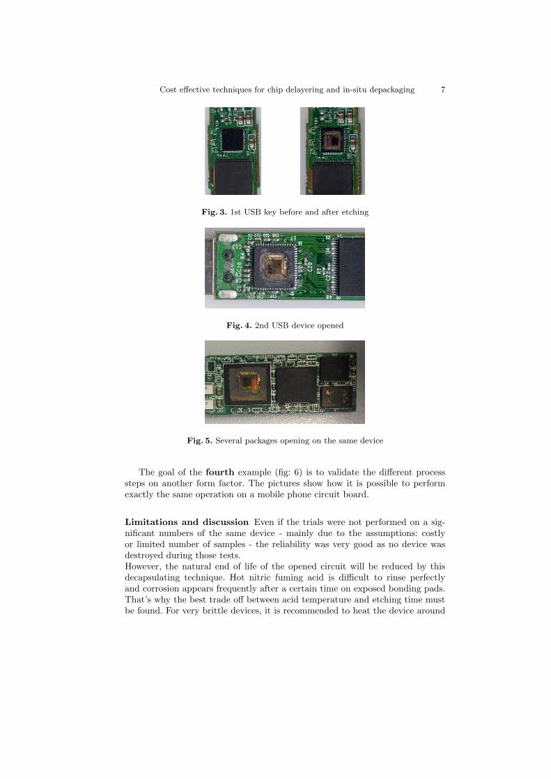
Cost effective techniques for chip delayering and in-situ depackaging 7
Fig. 3. 1st USB key before and after etching
Fig. 4. 2nd USB device opened
Fig. 5. Several packages opening on the same device
The goal of the fourth example (fig: 6) is to validate the different processsteps on another form factor. The pictures show how it is possible to performexactly the same operation on a mobile phone circuit board.
Limitations and discussion Even if the trials were not performed on a sig-nificant numbers of the same device - mainly due to the assumptions: costlyor limited number of samples - the reliability was very good as no device wasdestroyed during those tests.However, the natural end of life of the opened circuit will be reduced by thisdecapsulating technique. Hot nitric fuming acid is difficult to rinse perfectlyand corrosion appears frequently after a certain time on exposed bonding pads.That’s why the best trade off between acid temperature and etching time mustbe found. For very brittle devices, it is recommended to heat the device around

8 Philippe Loubet-Moundi
Fig. 6. in-situ depackaging applied on mobile phone circuit board
the acid temperature or to use ambient temperature for the etchant to avoidmechanical constraint due to thermal gradient during the operation.Minimizing the etching time could also be realized by performing chip packagethining with mechanical tools or ablation lasers.The presented solution can be used for many devices without dimensions andshapes limitations if the attacked package can be dissolved by standard acids(nitric, sulfuric).
3.2 Ultra low cost chip delayering
Purpose Once the chip has been decapsulated, deeper semi-invasive investiga-tions can be done in side-channel analysis or in fault attack injections. Delayeringtechniques could be used, as well, for chip reverse engineering or chip functionalblocks analysis. The purpose is to have access to buried layers that are coveredby security active shields or power routing shapes. As describe in the first partof this paper, those techniques usually requires dedicated expensive equipmentsor at least hazardous acids. The goal of the following tests is to measure andevaluate the capability to retreive hidden chip information with the minimumrequired equipment.
Methodology description This technique is inspired from parallel polish-ing with rotating plates with diamonds paste. The main difference is that therotating plate machine which cost around 20K Euros is replaced by manualmovements. A massive flat granite stone - from an anti-vibration stage - is usedas polishing material. The die surface is placed in contact with the stone and thepolishing movement was generated by applying smooth pressure with a fingeron the backside and by drawing some small circles. This manual polishing was

Cost effective techniques for chip delayering and in-situ depackaging 9
monitored frequently using an optical microscope. The results are presented inthe pictures below.
Results The trials were performed on a 130nm secure chip previously depack-aged with nitric acid. A security protection against probing - active shield - hidesthe deeper metal layers from observation. Without removing the top metal lay-ers, the localization of the different functional blocks like the memories, the logicpart or the analogue circuitry is impossible to achieve.
The pictures below were taken regularly for progression monitoring. The timeelapsed between the first and the last picture is around 1 hour.
Fig. 7. Results of 1 hour of manual polishing, low magnification
At low magnification, the results seems awful compared to others methodolo-gies. The parallelism is not preserved and the edges of the chip are etched fasterthan the middle. Small silicon particles fall from the edge of the die during theprocess and damaged the rest of the surface with scratches. However, if highermagnifications of the microscope are used, the result looks better.
The magnification level used for inspection is selected to have the smaller butthe better view of local parts of the die. Three areas were reported here after:the logic part, the NVM memory and the RAM memory.
– Logic areaThe microscope observation of local areas of the logic part of the circuit issurprisingly good. For the buried metal layers like M2 and M1, the qualitycould be sufficient to perform cell layout analysis of some small portions ofthe circuit.
– NVM areaIn the sample studied, the NVM represents a huge part of the chip area.This is quite interesting, as the polishing is not perfectly parallel, differentmetal layers can be observed at the same time. By consequence, the maindrawback is that there is no chance to take a clean picture of the entire NVMgrinded at the same metal level.
10 Philippe Loubet-Moundi
Fig. 8. Metal 2 (left) and Metal 1 (right) on the logic block of the chip
Fig. 9. Metal 4, Metal 3, Metal 2 and polysilicon levels on NVM area
– RAM area
Fig. 10. Metal 1 and polysilicon level on RAM array
Fig. 11. RAM cell at polysilicon level with after wet etching process (HF)

Cost effective techniques for chip delayering and in-situ depackaging 11
The last levels reached in delayering are the polysilicon or the substrateimplantation levels. The result obtained with the technique described inthis paper (fig: 10) is compared with sample preparation performed withHydrofluoric acid (HF) wet etching (fig: 11) on RAM area. The qualitybetween the both techniques is similar but the low cost mechanical samplepreparation allows to have also access to metal 1 (M1) which is not possiblewith basic HF layers removal.
Discussion The previous technique is the ultimate low cost technique as only aflat hard surface is needed. Of course, the results have a kind of randomness butthey are sufficient to extract useful information like the kind of memories used,the location of the logic or the analogue areas... High magnification pictures -where planarity of the entire chip is not mandatory - are in some case better thanwet etching. Obviously, without any improvement, this technique will not be usedby people who have better capabilities. But, this feasibility study could reallybe considered as an alternative for people who do not have skills or equipmentsin failure analysis and who want to start chip investigations with the minimumof budget.
4 Conclusion
In the trend of localized attacks, the present contribution shows that - even withlimited ressources - chip surface or hidden data in the die could be accessible.This paper has introduced a useful in-situ decapsulation technique for access-ing chip surface without performing desoldering operations. By consequence,soldered secure elements should not be considered more secure or more compli-cated to attack compared to standlone package. In addition, this paper has alsodemonstrated that low cost approaches could be developped for chip delayeringeven by people that do not have a background in failure analysis for the semi-conductors.
Fortunately, for the secure device provider - or unfortunately for the attacker- even with the results presented in this paper, performing semi-invasive or in-vasive attacks without expensive equipment will add more risks to damage thesample and the results obtained will remains far away from the state of the art.
However, the difficulty to perform satisfactory samples preparation will con-tinue to be underestimated or not really taken into account during attack quo-tations. This can be explained easily, because most of evaluation labs can easilyuse expensive failure analysis equipments. In addition, for those experts who areperforming daily sample preparations, accessing the chip surface, or performingreliable metal layer removal is an obvious and easy task. The massive introduc-tion of copper and low-k insulation materials for advanced semiconductor tech-nology nodes or the development of 3D integration process will probably providethem more challenging perspectives. Then, sample preparation techniques will

12 Philippe Loubet-Moundi
may be better considered during attack quotations. But for the time being, thesecurity of the product will be the same, whatever the package used.
Remark: The related presentation of this paper was done during the short-tracks session of COSADE 2013.
References
1. https://berlin.ccc.de/wiki/Experiment:_IC-Entkapselung_mit_
Kolophonium2. http://www.ultratecusa.com/decapsulation3. http://www.metcal.com/aprseries/4. http://www.oxford-instruments.com/products/etching-deposition-and-growth/
processes/etching-processes/organics/pi-etch5. Anderson, R., Kuhn, M.: Low cost attacks on tamper-resistant devices. In: Security
Protocols 5th International Workshop. pp. 125–136 (1997)6. Beck, F.: Integrated circuit failure analysis: a guide to preparation techniques.
Wiley series in quality and reliability engineering, Wiley (1998)7. Dehbaoui, A., Dutertre, J.M., Robisson, B., Tria, A.: Electromagnetic transient
faults injection on a hardware and software implementation of aes. In: FDTCproceedings. pp. 7–15. IEEE-CPS (2012)
8. Fournier, J., Loubet-Moundi, P.: Memory address scrambling reveals using faultattacks. In: Fault Diagnostic and Tolerance in Cryptography. pp. 30–36. FDTC ’10(2010)
9. Gandolfi, K., Mourtel, C., Olivier, F.: Electromagnetic analysis: Concrete results.In: CHES proceedings. Springer-Verlag (2001)
10. Laackmann, P., Janke, M.: Uncaging microchips. In: 31C3 (2013)11. Maurine, P.: Electromagnetic transient faults injection on a hardware and software
implementation of aes. In: FDTC proceedings. pp. 7–15. IEEE-CPS (2012)12. Nohl, K., Evans, D., Starbug, Plotz, H.: Reverse-engineering a cryptographic rfid
tag. In: USENIX Security Symposium (2008)13. Poucheret, F., K.Tobich, Lisart, M., B.Robisson, Chusseau, L., Maurine, P.: Local
and direct electromagnetic injection of power into cmos integrated circuits. In:FDTC’11 proceedings. pp. 100–104 (2011)
14. Schloesser, A., Nedospasov, D., Kraemer, J., Orlic, S., Seifert, J.P.: Simple photonicemission analysis of aes. In: CHES proceedings. pp. 41–57. Springer (2012)
15. Schmidt, J.M., Hutter, M., Plos, T.: Optical fault attacks on aes: A threat inviolet. In: Naccache, D., Oswald, E. (eds.) 6th Workshop on Fault Diagnosis andTolerance in Cryptography - FDTC 2009. pp. 13 – 22. IEEE-CS Press (2009)
16. Skorobogatov, S.: Semi-invasive attacks - a new approach to hardware securityanalysis,’ university of cambridge, technical report 630. Tech. rep. (2005)
17. Skorobogatov, S.: Flash memory ’bumping’ attacks. In: Proceedings of the 12thinternational conference on Cryptographic hardware and embedded systems. pp.158–172. CHES’10, Springer-Verlag, Berlin, Heidelberg (2010)
18. Skorobogatov, S.P., Anderson, R.J.: Optical fault induction attacks. In: CHESproceedings. pp. 2–12. Springer-Verlag (2002)
19. Skorobogatovi, S.: Local heating attacks on flash memory devices. In: Proceedingsof the 2nd IEEE International Workshop on Hardware-Oriented Security and Trust.HOST 2009 (2009)
20. Tobich, K., Maurine, P., Liardet, P.Y., Ordas, T.: Yet another fault injection tech-nique by forward bias injection. Tech. rep. (2012)


![Sulfuric Acid is[1]](https://img.pdfslide.us/doc/110x75/552847e14a7959c93d8b4684/sulfuric-acid-is1.jpg)