Embed Size (px)
Citation preview
Full PaperMacromolecularChemistry and Physics
(1 of 11) 1700135© 2017 WILEY-VCH Verlag GmbH & Co. KGaA, Weinheim wileyonlinelibrary.com DOI: 10.1002/macp.201700135
Coplanar Donor–Acceptor Semiconducting Copolymers to Achieve Better Conjugated Structures: Side-Chain Engineering
Mingyuan Pei, Ji-Hoon Kim, Sungmin On, Han-Koo Lee, Kilwon Cho,* Do-Hoon Hwang,* Hoichang Yang*
It is reported on the allocation effects of branched alkyl chains, when used as solubility and ordering enhancers of the conjugated donor–accepter (D–A) copolymer backbones, on the ordering and π–π overlapping of the copolymers, that drastically affect the electrical proper-ties of organic field-effect transistors (OFETs). Triisopropylsilylethynyl-benzo[1,2-b:4,5-b′]dith-iophene (TIPSBDT) and diketopyrrolopyrrole (DPP)-based copolymers, which have two linear alkyl spacers (methylene (C1) or butylene (C4)) between the DPP and side-substituent (C10H21)CH(C8H17), are synthesized by Suzuki cross-coupling. These copolymer films are spun cast onto a polymer-treated SiO2 dielectric surface, and some are further thermally annealed. The longer spacer, C4, is found to efficiently enhance the coplanarity and conjugation of the D–A back-bone, while the C1 does not. The resulting C4-bridged TIPSBDT-DPP-based copolymer readily develops a superior π-extended layer on the dielectric surface; the edge-on chains with ran-domly oriented side chains can be closely packed with a short π-planar distance (d(010)) of 3.57 Å. Its properties are superior to those of the short spacer C1 system with d(010) ≈3.93 Å. The C4-bridged TIPSBDT-DPP copolymer films yield a field-effect mobility up to 1.2 cm2 V−1 s−1 in OFETs, 12 times as higher than that of the C1 spacer system.
M. Pei, S. On, Prof. H. YangDepartment of Applied Organic Materials EngineeringInha UniversityIncheon 22212, South KoreaE-mail: [email protected]. J.-H. Kim, Prof. D.-H. HwangDepartment of Chemistry Chemistry Institute for Functional MaterialsPusan National University Busan 46241, South KoreaE-mail: [email protected]. H.-K. LeePohang Accelerator LaboratoryPohang 37673, South KoreaProf. K. ChoDepartment of Chemical EngineeringPOSTECH, Pohang 37673, South KoreaE-mail: [email protected]
1. Introduction
Organic field-effect transistors (OFETs) have attracted considerable research and industry attention because of their potential wearable device applications as low-cost, flexible, stretchable, and lightweight electronic compo-nents in wearable device displays, radio-frequency iden-tification tags, and sensors.[1,2] To achieve high electrical performance OFETs without any dopants, it is important to control the intra- and intermolecular ordering of the conjugated organic materials that serve as charge-carrier transport paths.[3–5] Unlike small molecules which can self-assemble into highly ordered domains,[6] conjugated polymers with high molecular-weight (Mw) tend to form a twisted or entangled chain conformation in solutions, preventing close π–π overlapping between these chains in solid states.[5] However, conjugated polymers possess
Macromol. Chem. Phys. , , 1700135
M. Pei et al.
www.mcp-journal.de
MacromolecularChemistry and Physics
© 2017 WILEY-VCH Verlag GmbH & Co. KGaA, Weinheim www.advancedsciencenews.com1700135 (2 of 11)
excellent deformability and high-temperature stability (greater than 250 °C), which make them more useful as active channel materials in flexible electronics compared to less-deformable small molecules.[2]
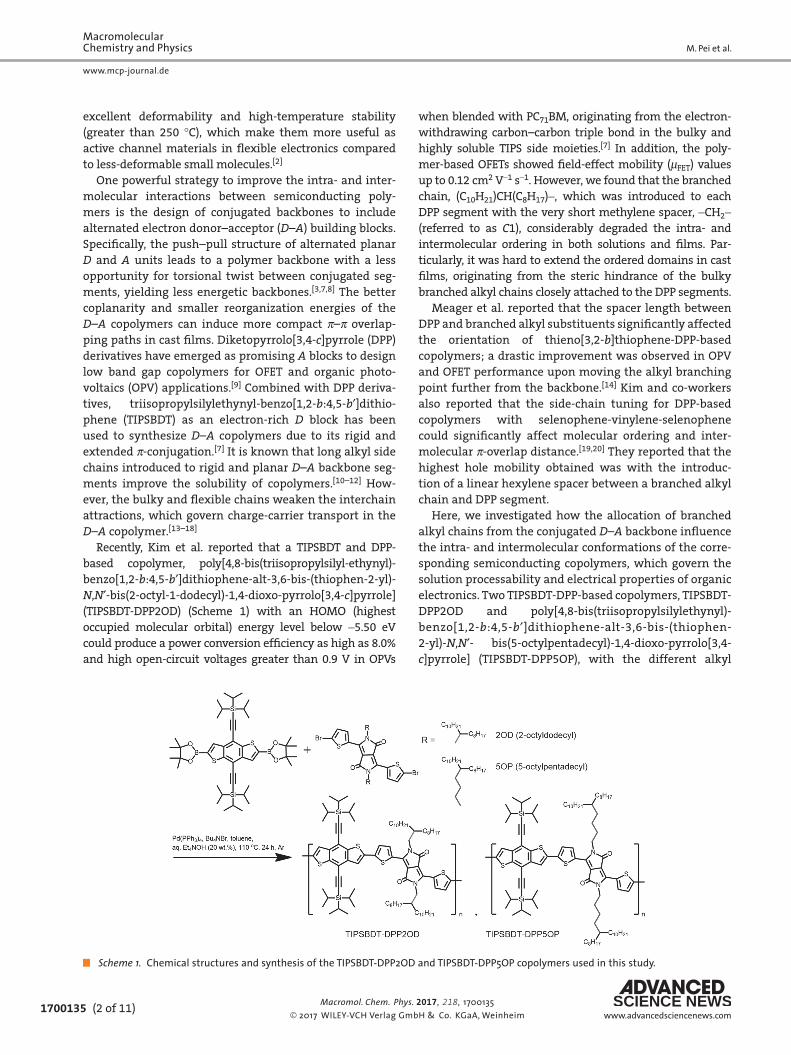
One powerful strategy to improve the intra- and inter-molecular interactions between semiconducting poly-mers is the design of conjugated backbones to include alternated electron donor–acceptor (D–A) building blocks. Specifically, the push–pull structure of alternated planar D and A units leads to a polymer backbone with a less opportunity for torsional twist between conjugated seg-ments, yielding less energetic backbones.[3,7,8] The better coplanarity and smaller reorganization energies of the D–A copolymers can induce more compact π–π overlap-ping paths in cast films. Diketopyrrolo[3,4-c]pyrrole (DPP) derivatives have emerged as promising A blocks to design low band gap copolymers for OFET and organic photo-voltaics (OPV) applications.[9] Combined with DPP deriva-tives, triisopropylsilylethynyl-benzo[1,2-b:4,5-b′]dithio-phene (TIPSBDT) as an electron-rich D block has been used to synthesize D–A copolymers due to its rigid and extended π-conjugation.[7] It is known that long alkyl side chains introduced to rigid and planar D–A backbone seg-ments improve the solubility of copolymers.[10–12] How-ever, the bulky and flexible chains weaken the interchain attractions, which govern charge-carrier transport in the D–A copolymer.[13–18]
Recently, Kim et al. reported that a TIPSBDT and DPP-based copolymer, poly[4,8-bis(triisopropylsilyl-ethynyl)-benzo[1,2-b:4,5-b′]dithiophene-alt-3,6-bis-(thiophen-2-yl)-N,N′-bis(2-octyl-1-dodecyl)-1,4-dioxo-pyrrolo[3,4-c]pyrrole] (TIPSBDT-DPP2OD) (Scheme 1) with an HOMO (highest occupied molecular orbital) energy level below −5.50 eV could produce a power conversion efficiency as high as 8.0% and high open-circuit voltages greater than 0.9 V in OPVs
when blended with PC71BM, originating from the electron-withdrawing carbon–carbon triple bond in the bulky and highly soluble TIPS side moieties.[7] In addition, the poly-mer-based OFETs showed field-effect mobility (μFET) values up to 0.12 cm2 V−1 s−1. However, we found that the branched chain, (C10H21)CH(C8H17)−, which was introduced to each DPP segment with the very short methylene spacer, −CH2− (referred to as C1), considerably degraded the intra- and intermolecular ordering in both solutions and films. Par-ticularly, it was hard to extend the ordered domains in cast films, originating from the steric hindrance of the bulky branched alkyl chains closely attached to the DPP segments.
Meager et al. reported that the spacer length between DPP and branched alkyl substituents significantly affected the orientation of thieno[3,2-b]thiophene-DPP-based copolymers; a drastic improvement was observed in OPV and OFET performance upon moving the alkyl branching point further from the backbone.[14] Kim and co-workers also reported that the side-chain tuning for DPP-based copolymers with selenophene-vinylene-selenophene could significantly affect molecular ordering and inter-molecular π-overlap distance.[19,20] They reported that the highest hole mobility obtained was with the introduc-tion of a linear hexylene spacer between a branched alkyl chain and DPP segment.
Here, we investigated how the allocation of branched alkyl chains from the conjugated D–A backbone influence the intra- and intermolecular conformations of the corre-sponding semiconducting copolymers, which govern the solution processability and electrical properties of organic electronics. Two TIPSBDT-DPP-based copolymers, TIPSBDT-DPP2OD and poly[4,8-bis(triisopropylsilylethynyl)-benzo[1,2-b:4,5-b′]dithiophene-alt-3,6-bis-(thiophen-2-yl)-N,N′- bis(5-octylpentadecyl)-1,4-dioxo-pyrrolo[3,4-c]pyrrole] (TIPSBDT-DPP5OP), with the different alkyl
Macromol. Chem. Phys. , , 1700135
Scheme 1. Chemical structures and synthesis of the TIPSBDT-DPP2OD and TIPSBDT-DPP5OP copolymers used in this study.
Coplanar Donor–Acceptor Semiconducting Copolymers to Achieve Better Conjugated Structures . . .
www.mcp-journal.de
MacromolecularChemistry and Physics
© 2017 WILEY-VCH Verlag GmbH & Co. KGaA, Weinheimwww.advancedsciencenews.com(3 of 11) 1700135
spacers (C1 and butylene (referred to as C4)) between the DPP and (C10H21)CH(C8H17)− chains, were synthesized by Suzuki cross-coupling (Scheme 1). The longer spacer, C4, drastically enhanced the coplanarity and conjugation of the TIPSBDT-DPP5OP copolymer, which had an Mw of 26 760 g mol−1 (smaller than the 35 790 g mol−1 of the TIPSBDT-DPP2OD copolymer). These D–A copolymer films were spun cast onto a polymer-treated silicon dioxide (SiO2) dielectric surface from chlorobenzene (CB) solu-tions, and some were further annealed at 200–300 °C. By inserting the longer spacer between DPP and (C10H21)CH(C8H17)−, the resulting TIPSBDT-DPP5OP copolymer could be tuned to form highly ordered and π-overlap extended domains of edge-on chains on the dielectric surface, with a narrow π–π overlap spacing (d(010)) up to 3.57 Å, in comparison to the less-conjugated short spacer system with a wider d(010) of 3.93 Å. Better ordering and shorter π–π overlapping provided TIPSBDT-DPP5OP OFETs with the benefit of a μFET value greater than 1.2 cm2 V−1 s−1, 12 times higher than that of the TIPSBDT-DPP2OD system. Proper side chains to minimize steric hindrance provide new insight into the molecular design of high-perfor-mance D–A copolymer-based semiconductors.
2. Results and Discussion
2.1. Material Characteristics
General characteristics of TIPSBDT-DPP-based copolymers synthesized by Suzuki cross-coupling (Scheme 1) are sum-marized in Table 1. Note that all copolymers used in this study were extracted from the synthesized powders by sox-hlet extraction with chloroform (CF). The chemical struc-tures of the TIPSBDT-DPP-based copolymers were identified by 1H-nuclear magnetic resonance (NMR) (Figures S1 and S2, Supporting Information). The number average mole cular weight (Mn) values of the TIPSBDT-DPP2OD and TIPSBDT-DPP5OP copolymers were 35 790, and 26 760 g mol−1, respectively, and the polydispersity index (PDI) values of the copolymers were 2.30 and 2.96, as determined by gel permeation chromatography (GPC) analysis (Figure S3,
Supporting Information). The relatively low-Mn of TIPSBDT-DPP5OP copolymer was mainly related to the decreased solubility driven by its enhanced coplanar structure.
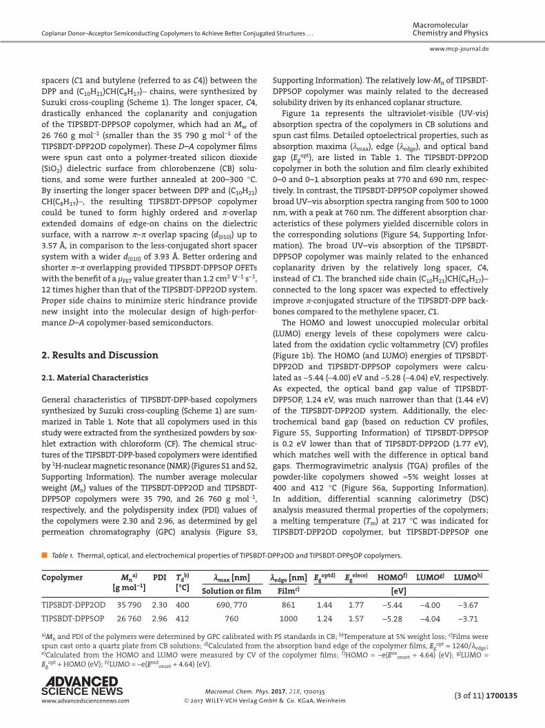
Figure 1a represents the ultraviolet-visible (UV-vis) absorption spectra of the copolymers in CB solutions and spun cast films. Detailed optoelectrical properties, such as absorption maxima (λmax), edge (λedge), and optical band gap (Eg
opt), are listed in Table 1. The TIPSBDT-DPP2OD copolymer in both the solution and film clearly exhibited 0–0 and 0–1 absorption peaks at 770 and 690 nm, respec-tively. In contrast, the TIPSBDT-DPP5OP copolymer showed broad UV–vis absorption spectra ranging from 500 to 1000 nm, with a peak at 760 nm. The different absorption char-acteristics of these polymers yielded discernible colors in the corresponding solutions (Figure S4, Supporting Infor-mation). The broad UV–vis absorption of the TIPSBDT-DPP5OP copolymer was mainly related to the enhanced coplanarity driven by the relatively long spacer, C4, instead of C1. The branched side chain (C10H21)CH(C8H17)− connected to the long spacer was expected to effectively improve π-conjugated structure of the TIPSBDT-DPP back-bones compared to the methylene spacer, C1.
The HOMO and lowest unoccupied molecular orbital (LUMO) energy levels of these copolymers were calcu-lated from the oxidation cyclic voltammetry (CV) profiles (Figure 1b). The HOMO (and LUMO) energies of TIPSBDT-DPP2OD and TIPSBDT-DPP5OP copolymers were calcu-lated as −5.44 (−4.00) eV and −5.28 (−4.04) eV, respectively. As expected, the optical band gap value of TIPSBDT-DPP5OP, 1.24 eV, was much narrower than that (1.44 eV) of the TIPSBDT-DPP2OD system. Additionally, the elec-trochemical band gap (based on reduction CV profiles, Figure S5, Supporting Information) of TIPSBDT-DPP5OP is 0.2 eV lower than that of TIPSBDT-DPP2OD (1.77 eV), which matches well with the difference in optical band gaps. Thermogravimetric analysis (TGA) profiles of the powder-like copolymers showed ≈5% weight losses at 400 and 412 °C (Figure S6a, Supporting Information). In addition, differential scanning calorimetry (DSC) analysis measured thermal properties of the copolymers; a melting temperature (Tm) at 217 °C was indicated for TIPSBDT-DPP2OD copolymer, but TIPSBDT-DPP5OP one
Macromol. Chem. Phys. , , 1700135
Table 1. Thermal, optical, and electrochemical properties of TIPSBDT-DPP2OD and TIPSBDT-DPP5OP copolymers.
Copolymer Mna)
[g mol−1]PDI Td
b) [°C]
λmax [nm] λedge [nm] Egoptd) Eg
elece) HOMOf) LUMOg) LUMOh)
Solution or film Filmc) [eV]
TIPSBDT-DPP2OD 35 790 2.30 400 690, 770 861 1.44 1.77 −5.44 −4.00 −3.67
TIPSBDT-DPP5OP 26 760 2.96 412 760 1000 1.24 1.57 −5.28 −4.04 −3.71
a)Mn and PDI of the polymers were determined by GPC calibrated with PS standards in CB; b)Temperature at 5% weight loss; c)Films were spun cast onto a quartz plate from CB solutions; d)Calculated from the absorption band edge of the copolymer films, Eg
opt = 1240/λedge; e)Calculated from the HOMO and LUMO were measured by CV of the copolymer films; f)HOMO = −e(Eox
onset + 4.64) (eV); g)LUMO = Eg
opt + HOMO (eV); h)LUMO = −e(Eredonset + 4.64) (eV).
M. Pei et al.
www.mcp-journal.de
MacromolecularChemistry and Physics
© 2017 WILEY-VCH Verlag GmbH & Co. KGaA, Weinheim www.advancedsciencenews.com1700135 (4 of 11)
did not show any endothermic peaks within the tempera-ture scanning range of 30–350 °C (Figure S6b, Supporting Information).
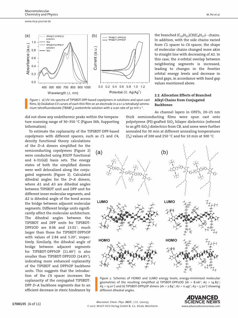
To estimate the coplanarity of the TIPSBDT-DPP-based copolymers with different spacers, such as C1 and C4, density functional theory calculations of the D–A dimers simplified for the semiconducting copolymers (Figure 2) were conducted using B3LYP functional and 6-31G(d) basis sets. The energy states of both the simplified dimers were well delocalized along the conju-gated segments (Figure 2). Calculated dihedral angles for the D–A dimers, where A1 and A3 are dihedral angles between TIPSBDT unit and DPP unit for different inner molecular segments, and A2 is dihedral angle of the bond across the bridge between adjacent molecular segments. Different bridge units signifi-cantly affect the molecular architecture. The dihedral angles between the TIPSBDT and DPP units for TIPSBDT-DPP2OD are 8.06 and 13.01°, much larger than those for TIPSBDT-DPP5OP with values of 2.84 and 5.20°, respec-tively. Similarly, the dihedral angle of bridge between adjacent segments for TIPSBDT-DPP5OP (11.49°) is also smaller than TIPSBDT-DPP2OD (14.85°), indicating more enhanced coplanarity of the TIPSBDT and DPP5OP backbone units. This suggests that the introduc-tion of the C4 spacer increases the coplanarity of the conjugated TIPSBDT-DPP D–A backbone segments due to an efficient decrease in steric hindrance by
the branched (C10H21)CH(C8H17)− chains. In addition, with the side chains varied from C1 spacer to C4 spacer, the shape of molecular chains changed more akin to straight line with decreasing of A2. In this case, the π-orbital overlap between neighboring segments is increased, leading to changes in the frontier orbital energy levels and decrease in band gaps, in accordance with band gap values mentioned above.
2.2. Allocation Effects of Branched Alkyl Chains from Conjugated Backbones
As channel layers in OFETs, 20–25 nm thick semiconducting films were spun cast onto polystyrene (PS)-grafted SiO2 bilayer dielectrics (referred to as gPS-SiO2) dielectrics from CB, and some were further annealed for 30 min at different annealing temperatures (TA) values of 200 and 250 °C and for 10 min at 300 °C.
Macromol. Chem. Phys. , , 1700135
Figure 1. a) UV–vis spectra of TIPSBDT-DPP-based copolymers in solutions and spun-cast films. b) Oxidation CV curves of each thin film on an electrode in a 0.1 m tetrabutyl ammo-nium tetrafluoroborate (TBABF4)-acetonitrile solution with a scan rate of 50 mV s−1.
Figure 2. Schemes of HOMO and LUMO energy levels, energy-minimized molecular geometries of the resulting simplified a) TIPSBDT-DPP2OD (A1 = 8.06°; A2 = 14.85°; A3 = 13.01°) and b) TIPSBDT-DPP5OP dimers (A1 = 2.84°; A2 = 11.49°; A3 = 5.20°) showing different dihedral angles.
Coplanar Donor–Acceptor Semiconducting Copolymers to Achieve Better Conjugated Structures . . .
www.mcp-journal.de
MacromolecularChemistry and Physics
© 2017 WILEY-VCH Verlag GmbH & Co. KGaA, Weinheimwww.advancedsciencenews.com(5 of 11) 1700135
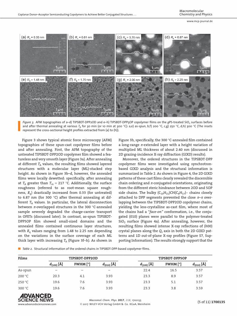
Figure 3 shows typical atomic force microscopy (AFM) topographies of these spun-cast copolymer films before and after annealing. First, the AFM topography of the untreated TIPSBDT-DPP2OD copolymer film showed a fea-tureless and very smooth layer (Figure 3a). After annealing at different TA values, the resulting films showed layered structures with a molecular layer (ML)-stacked step height. As shown in Figure 3b–d, however, the annealed films were locally dewetted: specifically, after annealing at TA greater than Tm = 217 °C. Additionally, the surface roughness (referred to as root-mean square rough-ness, Rq) drastically increased from 0.33 (for untreated) to 6.87 nm (for 300 °C) after thermal annealing at dif-ferent TA values. In particular, the lateral disconnection between π-overlapped structures in the 300 °C-annealed sample severely degraded the charge-carrier transport in OFETs (discussed later). In contrast, as-spun TIPSBDT-DPP5OP film showed small-sized domains and the annealed films contained continuous layer structures, with Rq values ranging from 1.48 to 2.25 nm depending on the variations in the surface coverage of each ML thick layer with increasing TA (Figure 3f–h). As shown in
Figure 3h, specifically, the 300 °C-annealed film contained a long-range π-extended layer with a height variation of multiplied ML thickness of about 2.40 nm (discussed in 2D grazing-incidence X-ray diffraction (GIXD) results).
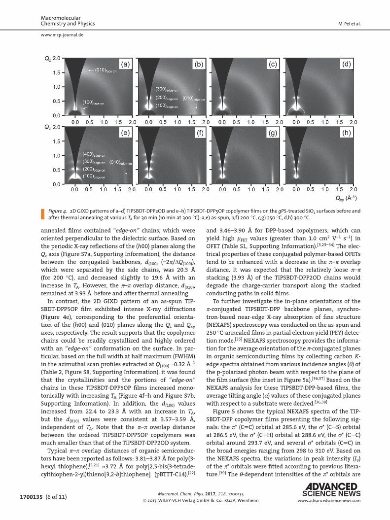
Moreover, the ordered structures in the TIPSBDT-DPP copolymer films were investigated using synchrotron-based GIXD analysis and the structural information is summarized in Table 2. As shown in Figure 4, the 2D GIXD patterns of these cast films clearly revealed the discernible chain ordering and π-conjugated orientations, originating from the different steric hindrance between 2OD and 5OP side chains. The bulky (C10H21)CH(C8H17)− chains closely attached to DPP segments prevented the close π–π over-lapping between the TIPSBDT-DPP2OD copolymer chains, yielding the less-crystalline as-cast film, where most of the chains had a “face-on” conformation, i.e., the conju-gated (010) planes were parallel to the polymer-treated SiO2 surface (Figure 4a). After annealing, however, the resulting films showed intense X-ray reflections of (h00) crystal planes along the Qz axis in both the 2D GIXD pat-terns and 1D out-of-plane X-ray profiles (Figure S7, Sup-porting Information). The results strongly support that the
Macromol. Chem. Phys. , , 1700135
Figure 3. AFM topographies of a–d) TIPSBDT-DPP2OD and e–h) TIPSBDT-DPP5OP copolymer films on the gPS-treated SiO2 surfaces before and after thermal annealing at various TA for 30 min (or 10 min at 300 °C): a,e) as-spun, b,f) 200 °C, c,g) 250 °C, d,h) 300 °C (The insets represent the cross-sectional height profiles extracted from (a) to (h)).
Table 2. Structural information of the ordered chains in TIPSBDT-DPP-based copolymer films.
Films TIPSBDT-DPP2OD TIPSBDT-DPP5OP
d(100) [Å] FWHM [°] d(010) [Å] d(100) [Å] FWHM [°] d(010) [Å]
As-spun – – – 22.4 16.5 3.57
200 °C 20.3 4.1 3.93 23.3 8.9 3.57
250 °C 19.6 7.6 3.93 23.3 5.1 3.57
300 °C 19.6 7.6 3.93 23.3 3.8 3.59
M. Pei et al.
www.mcp-journal.de
MacromolecularChemistry and Physics
© 2017 WILEY-VCH Verlag GmbH & Co. KGaA, Weinheim www.advancedsciencenews.com1700135 (6 of 11)
annealed films contained “edge-on” chains, which were oriented perpendicular to the dielectric surface. Based on the periodic X-ray reflections of the (h00) planes along the Qz axis (Figure S7a, Supporting Information), the distance between the conjugated backbones, d(100) (=2π/ΔQ(100)), which were separated by the side chains, was 20.3 Å (for 200 °C), and decreased slightly to 19.6 Å with an increase in TA. However, the π–π overlap distance, d(010), remained at 3.93 Å, before and after thermal annealing.
In contrast, the 2D GIXD pattern of an as-spun TIP-SBDT-DPP5OP film exhibited intense X-ray diffractions (Figure 4e), corresponding to the preferential orienta-tion of the (h00) and (010) planes along the Qz and Qxy axes, respectively. The result supports that the copolymer chains could be readily crystallized and highly ordered with an “edge-on” conformation on the surface. In par-ticular, based on the full width at half maximum (FWHM) in the azimuthal scan profiles extracted at Q(100) ≈0.32 Å−1 (Table 2, Figure S8, Supporting Information), it was found that the crystallinities and the portions of “edge-on” chains in these TIPSBDT-DPP5OP films increased mono-tonically with increasing TA (Figure 4f–h and Figure S7b, Supporting Information). In addition, the d(100) values increased from 22.4 to 23.3 Å with an increase in TA, but the d(010) values were consistent at 3.57–3.59 Å, independent of TA. Note that the π–π overlap distance between the ordered TIPSBDT-DPP5OP copolymers was much smaller than that of the TIPSBDT-DPP2OD system.
Typical π–π overlap distances of organic semiconduc-tors have been reported as follows: 3.81–3.87 Å for poly(3-hexyl thiophene),[5,21] ≈3.72 Å for poly[2,5-bis(3-tetrade-cylthiophen-2-yl)thieno[3,2-b]thiophene] (pBTTT-C14),[22]
and 3.46–3.90 Å for DPP-based copolymers, which can yield high μFET values (greater than 1.0 cm2 V−1 s−1) in OFET (Table S1, Supporting Information).[3,23–34] The elec-trical properties of these conjugated polymer-based OFETs tend to be enhanced with a decrease in the π–π overlap distance. It was expected that the relatively loose π–π stacking (3.93 Å) of the TIPSBDT-DPP2OD chains would degrade the charge-carrier transport along the stacked conducting paths in solid films.
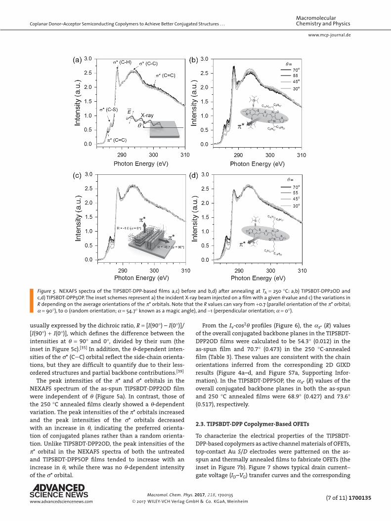
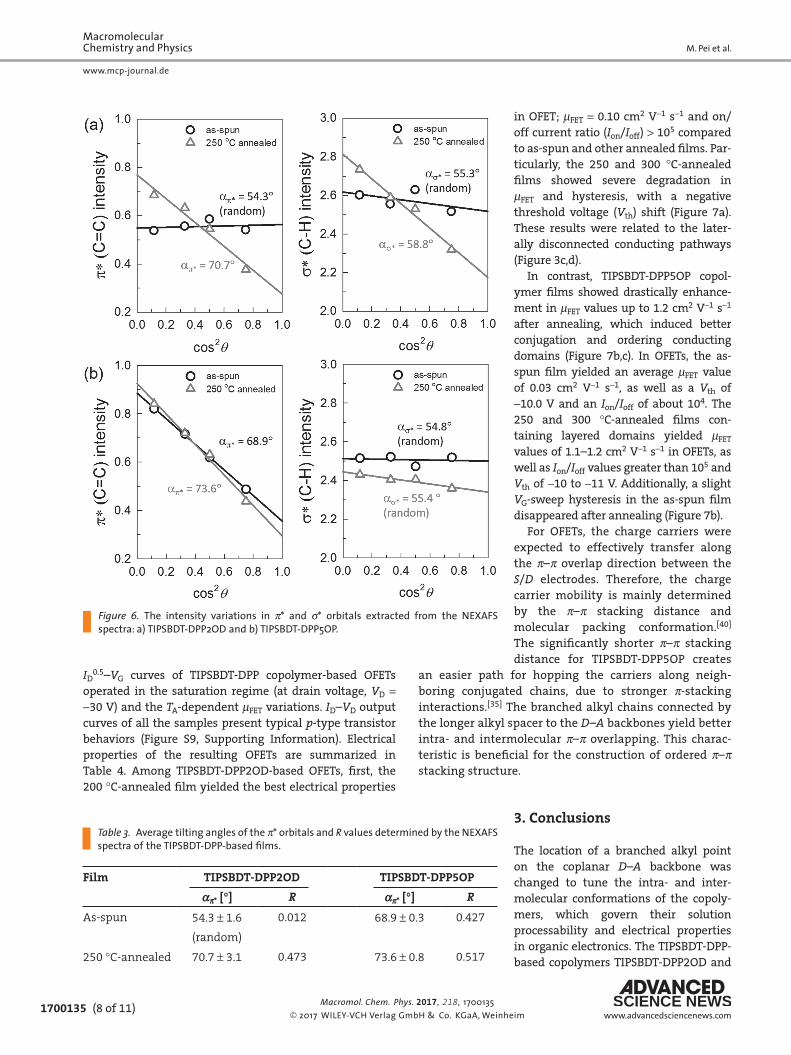
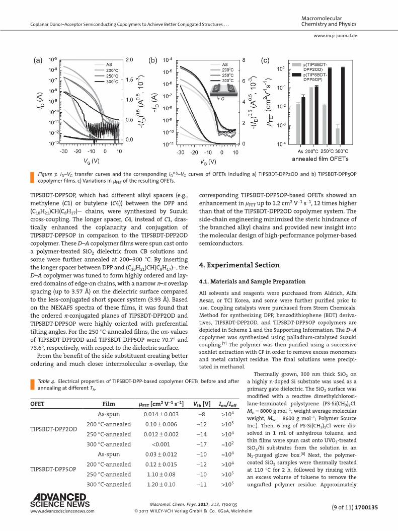
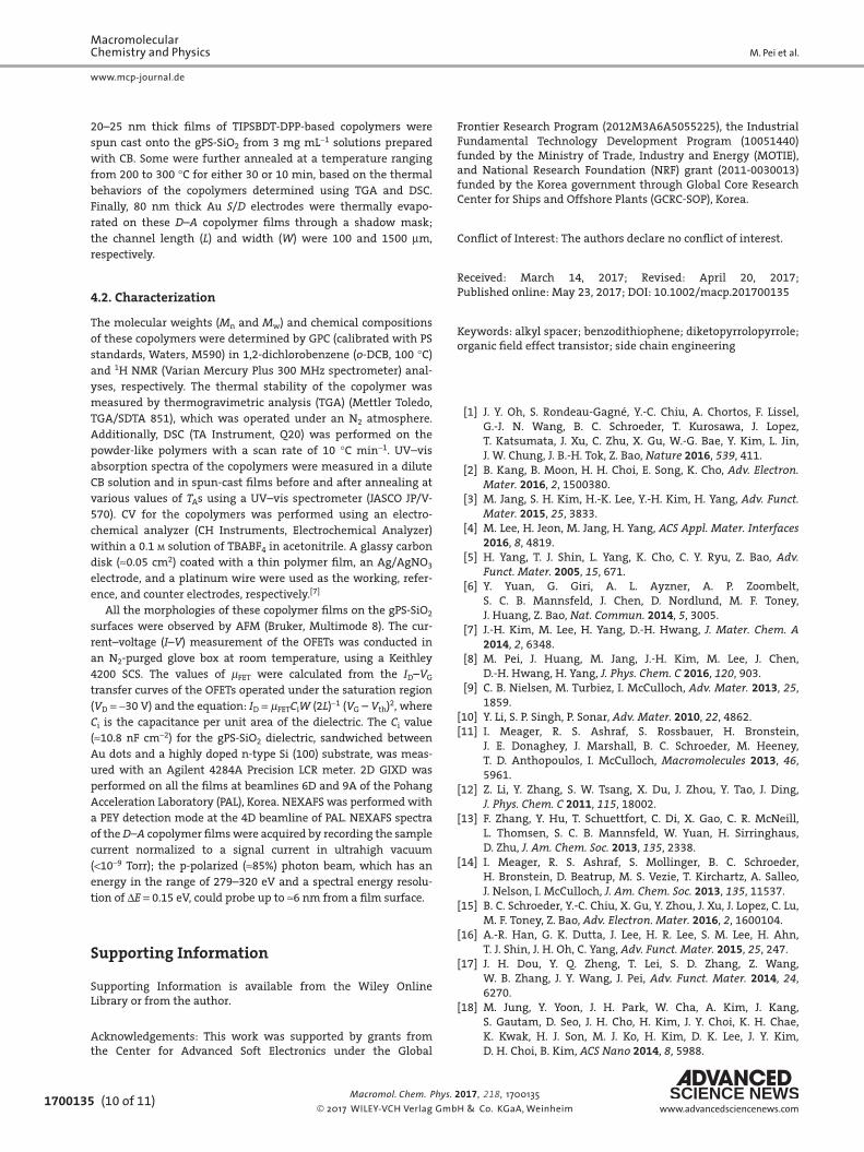
To further investigate the in-plane orientations of the π-conjugated TIPSBDT-DPP backbone planes, synchro-tron-based near-edge X-ray absorption of fine structure (NEXAFS) spectroscopy was conducted on the as-spun and 250 °C-annealed films in partial electron yield (PEY) detec-tion mode.[35] NEXAFS spectroscopy provides the informa-tion for the average orientation of the π-conjugated planes in organic semiconducting films by collecting carbon K-edge spectra obtained from various incidence angles (θ) of the p-polarized photon beam with respect to the plane of the film surface (the inset in Figure 5a).[36,37] Based on the NEXAFS analysis for these TIPSBDT-DPP-based films, the average tilting angle (α) values of these conjugated planes with respect to a substrate were derived.[36,38]
Figure 5 shows the typical NEXAFS spectra of the TIP-SBDT-DPP copolymer films presenting the following sig-nals: the π* (CC) orbital at 285.6 eV, the σ* (CS) orbital at 286.5 eV, the σ* (CH) orbital at 288.6 eV, the σ* (CC) orbital around 293.7 eV, and several σ* orbitals (CC) in the broad energies ranging from 298 to 310 eV. Based on the NEXAFS spectra, the variations in peak intensity (Iv) of the π* orbitals were fitted according to previous litera-ture.[39] The θ-dependent intensities of the π* orbitals are
Macromol. Chem. Phys. , , 1700135
Figure 4. 2D GIXD patterns of a–d) TIPSBDT-DPP2OD and e–h) TIPSBDT-DPP5OP copolymer films on the gPS-treated SiO2 surfaces before and after thermal annealing at various TA for 30 min (10 min at 300 °C): a,e) as-spun, b,f) 200 °C, c,g) 250 °C, d,h) 300 °C.
Coplanar Donor–Acceptor Semiconducting Copolymers to Achieve Better Conjugated Structures . . .
www.mcp-journal.de
MacromolecularChemistry and Physics
© 2017 WILEY-VCH Verlag GmbH & Co. KGaA, Weinheimwww.advancedsciencenews.com(7 of 11) 1700135
usually expressed by the dichroic ratio, R = [I(90°) – I(0°)]/[I(90°) + I(0°)], which defines the difference between the intensities at θ = 90° and 0°, divided by their sum (the inset in Figure 5c).[35] In addition, the θ-dependent inten-sities of the σ* (CC) orbital reflect the side-chain orienta-tions, but they are difficult to quantify due to their less-ordered structures and partial backbone contributions.[39]
The peak intensities of the π* and σ* orbitals in the NEXAFS spectrum of the as-spun TIPSBDT-DPP2OD film were independent of θ (Figure 5a). In contrast, those of the 250 °C annealed films clearly showed a θ-dependent variation. The peak intensities of the π* orbitals increased and the peak intensities of the σ* orbitals decreased with an increase in θ, indicating the preferred orienta-tion of conjugated planes rather than a random orienta-tion. Unlike TIPSBDT-DPP2OD, the peak intensities of the π* orbital in the NEXAFS spectra of both the untreated and TIPSBDT-DPP5OP films tended to increase with an increase in θ, while there was no θ-dependent intensity of the σ* orbital.
From the Iv-cos2θ profiles (Figure 6), the απ* (R) values of the overall conjugated backbone planes in the TIPSBDT-DPP2OD films were calculated to be 54.3° (0.012) in the as-spun film and 70.7° (0.473) in the 250 °C-annealed film (Table 3). These values are consistent with the chain orientations inferred from the corresponding 2D GIXD results (Figure 4a–d, and Figure S7a, Supporting Infor-mation). In the TIPSBDT-DPP5OP, the απ* (R) values of the overall conjugated backbone planes in both the as-spun and 250 °C annealed films were 68.9° (0.427) and 73.6° (0.517), respectively.
2.3. TIPSBDT-DPP Copolymer-Based OFETs
To characterize the electrical properties of the TIPSBDT-DPP-based copolymers as active channel materials of OFETs, top-contact Au S/D electrodes were patterned on the as-spun and thermally annealed films to fabricate OFETs (the inset in Figure 7b). Figure 7 shows typical drain current−gate voltage (ID–VG) transfer curves and the corresponding
Macromol. Chem. Phys. , , 1700135
Figure 5. NEXAFS spectra of the TIPSBDT-DPP-based films a,c) before and b,d) after annealing at TA = 250 °C: a,b) TIPSBDT-DPP2OD and c,d) TIPSBDT-DPP5OP. The inset schemes represent a) the incident X-ray beam injected on a film with a given θ value and c) the variations in R depending on the average orientations of the π* orbitals. Note that the R values can vary from +0.7 (parallel orientation of the π* orbital; α = 90°), to 0 (random orientation; α = 54.7° known as a magic angle), and −1 (perpendicular orientation; α = 0°).
M. Pei et al.
www.mcp-journal.de
MacromolecularChemistry and Physics
© 2017 WILEY-VCH Verlag GmbH & Co. KGaA, Weinheim www.advancedsciencenews.com1700135 (8 of 11)
ID0.5–VG curves of TIPSBDT-DPP copolymer-based OFETs
operated in the saturation regime (at drain voltage, VD = −30 V) and the TA-dependent μFET variations. ID–VD output curves of all the samples present typical p-type transistor behaviors (Figure S9, Supporting Information). Electrical properties of the resulting OFETs are summarized in Table 4. Among TIPSBDT-DPP2OD-based OFETs, first, the 200 °C-annealed film yielded the best electrical properties
in OFET; μFET = 0.10 cm2 V−1 s−1 and on/off current ratio (Ion/Ioff) > 105 compared to as-spun and other annealed films. Par-ticularly, the 250 and 300 °C-annealed films showed severe degradation in μFET and hysteresis, with a negative threshold voltage (Vth) shift (Figure 7a). These results were related to the later-ally disconnected conducting pathways (Figure 3c,d).
In contrast, TIPSBDT-DPP5OP copol-ymer films showed drastically enhance-ment in μFET values up to 1.2 cm2 V−1 s−1 after annealing, which induced better conjugation and ordering conducting domains (Figure 7b,c). In OFETs, the as-spun film yielded an average μFET value of 0.03 cm2 V−1 s−1, as well as a Vth of −10.0 V and an Ion/Ioff of about 104. The 250 and 300 °C-annealed films con-taining layered domains yielded μFET values of 1.1–1.2 cm2 V−1 s−1 in OFETs, as well as Ion/Ioff values greater than 105 and Vth of −10 to −11 V. Additionally, a slight VG-sweep hysteresis in the as-spun film disappeared after annealing (Figure 7b).
For OFETs, the charge carriers were expected to effectively transfer along the π–π overlap direction between the S/D electrodes. Therefore, the charge carrier mobility is mainly determined by the π–π stacking distance and molecular packing conformation.[40] The significantly shorter π–π stacking distance for TIPSBDT-DPP5OP creates
an easier path for hopping the carriers along neigh-boring conjugated chains, due to stronger π-stacking interactions.[35] The branched alkyl chains connected by the longer alkyl spacer to the D–A backbones yield better intra- and intermolecular π–π overlapping. This charac-teristic is beneficial for the construction of ordered π–π stacking structure.
3. Conclusions
The location of a branched alkyl point on the coplanar D–A backbone was changed to tune the intra- and inter-molecular conformations of the copoly-mers, which govern their solution processability and electrical properties in organic electronics. The TIPSBDT-DPP-based copolymers TIPSBDT-DPP2OD and
Macromol. Chem. Phys. , , 1700135
Figure 6. The intensity variations in π* and σ* orbitals extracted from the NEXAFS spectra: a) TIPSBDT-DPP2OD and b) TIPSBDT-DPP5OP.
Table 3. Average tilting angles of the π* orbitals and R values determined by the NEXAFS spectra of the TIPSBDT-DPP-based films.
Film TIPSBDT-DPP2OD TIPSBDT-DPP5OP
απ* [°] R απ* [°] R
As-spun 54.3 ± 1.6 0.012 68.9 ± 0.3 0.427
(random)
250 °C-annealed 70.7 ± 3.1 0.473 73.6 ± 0.8 0.517
Coplanar Donor–Acceptor Semiconducting Copolymers to Achieve Better Conjugated Structures . . .
www.mcp-journal.de
MacromolecularChemistry and Physics
© 2017 WILEY-VCH Verlag GmbH & Co. KGaA, Weinheimwww.advancedsciencenews.com(9 of 11) 1700135
Macromol. Chem. Phys. , , 1700135
TIPSBDT-DPP5OP, which had different alkyl spacers (e.g., methylene (C1) or butylene (C4)) between the DPP and (C10H21)CH(C8H17) chains, were synthesized by Suzuki cross-coupling. The longer spacer, C4, instead of C1, dras-tically enhanced the coplanarity and conjugation of TIPSBDT-DPP5OP in comparison to the TIPSBDT-DPP2OD copolymer. These D–A copolymer films were spun cast onto a polymer-treated SiO2 dielectric from CB solutions and some were further annealed at 200–300 °C. By inserting the longer spacer between DPP and (C10H21)CH(C8H17)−, the D–A copolymer was tuned to form highly ordered and lay-ered domains of edge-on chains, with a narrow π–π overlap spacing (up to 3.57 Å) on the dielectric surface compared to the less-conjugated short spacer system (3.93 Å). Based on the NEXAFS spectra of these films, it was found that the ordered π-conjugated planes of TIPSBDT-DPP2OD and TIPSBDT-DPP5OP were highly oriented with preferential tilting angles. For the 250 °C-annealed films, the απ* values of TIPSBDT-DPP2OD and TIPSBDT-DPP5OP were 70.7° and 73.6°, respectively, with respect to the dielectric surface.
From the benefit of the side substituent creating better ordering and much closer intermolecular π-overlap, the
corresponding TIPSBDT-DPP5OP-based OFETs showed an enhancement in μFET up to 1.2 cm2 V−1 s−1, 12 times higher than that of the TIPSBDT-DPP2OD copolymer system. The side-chain engineering minimized the steric hindrance of the branched alkyl chains and provided new insight into the molecular design of high-performance polymer-based semiconductors.
4. Experimental Section
4.1. Materials and Sample Preparation
All solvents and reagents were purchased from Aldrich, Alfa Aesar, or TCI Korea, and some were further purified prior to use. Coupling catalysts were purchased from Strem Chemicals. Method for synthesizing DPP, benzodithiophene (BDT) deriva-tives, TIPSBDT-DPP2OD, and TIPSBDT-DPP5OP copolymers are depicted in Scheme 1 and the Supporting Information. The D–A copolymer was synthesized using palladium-catalyzed Suzuki coupling.[7] The polymer was then purified using a successive soxhlet extraction with CF in order to remove excess monomers and metal catalyst residue. The final solutions were precipi-tated in methanol.
Thermally grown, 300 nm thick SiO2 on a highly n-doped Si substrate was used as a primary gate dielectric. The SiO2 surface was modified with a reactive dimethylchlorosi-lane-terminated polystyrene (PS-Si(CH3)2Cl, Mn = 8000 g mol−1; weight average mole cular weight, Mw = 8600 g mol−1; Polymer Source Inc.). Then, 6 mg of PS-Si(CH3)2Cl were dis-solved in 1 mL of anhydrous toluene, and thin films were spun cast onto UVO3-treated SiO2/Si substrates from the solution in an N2-purged glove box.[8] Next, the polymer-coated SiO2 samples were thermally treated at 110 °C for 2 h, followed by rinsing with an excess volume of toluene to remove the ungrafted polymer residue. Approximately
Figure 7. ID–VG transfer curves and the corresponding ID0.5–VG curves of OFETs including a) TIPSBDT-DPP2OD and b) TIPSBDT-DPP5OP
copoly mer films. c) Variations in μFET of the resulting OFETs.
Table 4. Electrical properties of TIPSBDT-DPP-based copolymer OFETs, before and after annealing at different TA.
OFET Film μFET [cm2 V−1 s−1] Vth [V] Ion/Ioff
TIPSBDT-DPP2OD
As-spun 0.014 ± 0.003 −8 >104
200 °C-annealed 0.10 ± 0.006 −12 >105
250 °C-annealed 0.012 ± 0.002 −14 >104
300 °C-annealed <0.001 −17 ≈102
TIPSBDT-DPP5OP
As-spun 0.03 ± 0.012 −10 ≈104
200 °C-annealed 0.12 ± 0.015 −12 >104
250 °C-annealed 1.10 ± 0.08 −10 >105
300 °C-annealed 1.20 ± 0.10 −11 >105
M. Pei et al.
www.mcp-journal.de
MacromolecularChemistry and Physics
© 2017 WILEY-VCH Verlag GmbH & Co. KGaA, Weinheim www.advancedsciencenews.com1700135 (10 of 11)
Macromol. Chem. Phys. , , 1700135
20–25 nm thick films of TIPSBDT-DPP-based copolymers were spun cast onto the gPS-SiO2 from 3 mg mL−1 solutions prepared with CB. Some were further annealed at a temperature ranging from 200 to 300 °C for either 30 or 10 min, based on the thermal behaviors of the copolymers determined using TGA and DSC. Finally, 80 nm thick Au S/D electrodes were thermally evapo-rated on these D–A copolymer films through a shadow mask; the channel length (L) and width (W) were 100 and 1500 μm, respectively.
4.2. Characterization
The molecular weights (Mn and Mw) and chemical compositions of these copolymers were determined by GPC (calibrated with PS standards, Waters, M590) in 1,2-dichlorobenzene (o-DCB, 100 °C) and 1H NMR (Varian Mercury Plus 300 MHz spectrometer) anal-yses, respectively. The thermal stability of the copolymer was measured by thermogravimetric analysis (TGA) (Mettler Toledo, TGA/SDTA 851), which was operated under an N2 atmosphere. Additionally, DSC (TA Instrument, Q20) was performed on the powder-like polymers with a scan rate of 10 °C min−1. UV–vis absorption spectra of the copolymers were measured in a dilute CB solution and in spun-cast films before and after annealing at various values of TAs using a UV–vis spectrometer (JASCO JP/V-570). CV for the copolymers was performed using an electro-chemical analyzer (CH Instruments, Electrochemical Analyzer) within a 0.1 m solution of TBABF4 in acetonitrile. A glassy carbon disk (≈0.05 cm2) coated with a thin polymer film, an Ag/AgNO3 electrode, and a platinum wire were used as the working, refer-ence, and counter electrodes, respectively.[7]
All the morphologies of these copolymer films on the gPS-SiO2 surfaces were observed by AFM (Bruker, Multimode 8). The cur-rent–voltage (I–V) measurement of the OFETs was conducted in an N2-purged glove box at room temperature, using a Keithley 4200 SCS. The values of μFET were calculated from the ID–VG transfer curves of the OFETs operated under the saturation region (VD = −30 V) and the equation: ID = μFETCiW (2L)−1 (VG – Vth)2, where Ci is the capacitance per unit area of the dielectric. The Ci value (≈10.8 nF cm−2) for the gPS-SiO2 dielectric, sandwiched between Au dots and a highly doped n-type Si (100) substrate, was meas-ured with an Agilent 4284A Precision LCR meter. 2D GIXD was performed on all the films at beamlines 6D and 9A of the Pohang Acceleration Laboratory (PAL), Korea. NEXAFS was performed with a PEY detection mode at the 4D beamline of PAL. NEXAFS spectra of the D–A copolymer films were acquired by recording the sample current normalized to a signal current in ultrahigh vacuum (<10−9 Torr); the p-polarized (≈85%) photon beam, which has an energy in the range of 279–320 eV and a spectral energy resolu-tion of ΔE = 0.15 eV, could probe up to ≈6 nm from a film surface.
Supporting Information
Supporting Information is available from the Wiley Online Library or from the author.
Acknowledgements: This work was supported by grants from the Center for Advanced Soft Electronics under the Global
Frontier Research Program (2012M3A6A5055225), the Industrial Fundamental Technology Development Program (10051440) funded by the Ministry of Trade, Industry and Energy (MOTIE), and National Research Foundation (NRF) grant (2011-0030013) funded by the Korea government through Global Core Research Center for Ships and Offshore Plants (GCRC-SOP), Korea.
Conflict of Interest: The authors declare no conflict of interest.
Received: March 14, 2017; Revised: April 20, 2017; Published online: May 23, 2017; DOI: 10.1002/macp.201700135
Keywords: alkyl spacer; benzodithiophene; diketopyrrolopyrrole; organic field effect transistor; side chain engineering
[1] J. Y. Oh, S. Rondeau-Gagné, Y.-C. Chiu, A. Chortos, F. Lissel, G.-J. N. Wang, B. C. Schroeder, T. Kurosawa, J. Lopez, T. Katsumata, J. Xu, C. Zhu, X. Gu, W.-G. Bae, Y. Kim, L. Jin, J. W. Chung, J. B.-H. Tok, Z. Bao, Nature 2016, 539, 411.
[2] B. Kang, B. Moon, H. H. Choi, E. Song, K. Cho, Adv. Electron. Mater. 2016, 2, 1500380.
[3] M. Jang, S. H. Kim, H.-K. Lee, Y.-H. Kim, H. Yang, Adv. Funct. Mater. 2015, 25, 3833.
[4] M. Lee, H. Jeon, M. Jang, H. Yang, ACS Appl. Mater. Interfaces 2016, 8, 4819.
[5] H. Yang, T. J. Shin, L. Yang, K. Cho, C. Y. Ryu, Z. Bao, Adv. Funct. Mater. 2005, 15, 671.
[6] Y. Yuan, G. Giri, A. L. Ayzner, A. P. Zoombelt, S. C. B. Mannsfeld, J. Chen, D. Nordlund, M. F. Toney, J. Huang, Z. Bao, Nat. Commun. 2014, 5, 3005.
[7] J.-H. Kim, M. Lee, H. Yang, D.-H. Hwang, J. Mater. Chem. A 2014, 2, 6348.
[8] M. Pei, J. Huang, M. Jang, J.-H. Kim, M. Lee, J. Chen, D.-H. Hwang, H. Yang, J. Phys. Chem. C 2016, 120, 903.
[9] C. B. Nielsen, M. Turbiez, I. McCulloch, Adv. Mater. 2013, 25, 1859.
[10] Y. Li, S. P. Singh, P. Sonar, Adv. Mater. 2010, 22, 4862.[11] I. Meager, R. S. Ashraf, S. Rossbauer, H. Bronstein,
J. E. Donaghey, J. Marshall, B. C. Schroeder, M. Heeney, T. D. Anthopoulos, I. McCulloch, Macromolecules 2013, 46, 5961.
[12] Z. Li, Y. Zhang, S. W. Tsang, X. Du, J. Zhou, Y. Tao, J. Ding, J. Phys. Chem. C 2011, 115, 18002.
[13] F. Zhang, Y. Hu, T. Schuettfort, C. Di, X. Gao, C. R. McNeill, L. Thomsen, S. C. B. Mannsfeld, W. Yuan, H. Sirringhaus, D. Zhu, J. Am. Chem. Soc. 2013, 135, 2338.
[14] I. Meager, R. S. Ashraf, S. Mollinger, B. C. Schroeder, H. Bronstein, D. Beatrup, M. S. Vezie, T. Kirchartz, A. Salleo, J. Nelson, I. McCulloch, J. Am. Chem. Soc. 2013, 135, 11537.
[15] B. C. Schroeder, Y.-C. Chiu, X. Gu, Y. Zhou, J. Xu, J. Lopez, C. Lu, M. F. Toney, Z. Bao, Adv. Electron. Mater. 2016, 2, 1600104.
[16] A.-R. Han, G. K. Dutta, J. Lee, H. R. Lee, S. M. Lee, H. Ahn, T. J. Shin, J. H. Oh, C. Yang, Adv. Funct. Mater. 2015, 25, 247.
[17] J. H. Dou, Y. Q. Zheng, T. Lei, S. D. Zhang, Z. Wang, W. B. Zhang, J. Y. Wang, J. Pei, Adv. Funct. Mater. 2014, 24, 6270.
[18] M. Jung, Y. Yoon, J. H. Park, W. Cha, A. Kim, J. Kang, S. Gautam, D. Seo, J. H. Cho, H. Kim, J. Y. Choi, K. H. Chae, K. Kwak, H. J. Son, M. J. Ko, H. Kim, D. K. Lee, J. Y. Kim, D. H. Choi, B. Kim, ACS Nano 2014, 8, 5988.
Coplanar Donor–Acceptor Semiconducting Copolymers to Achieve Better Conjugated Structures . . .
www.mcp-journal.de
MacromolecularChemistry and Physics
© 2017 WILEY-VCH Verlag GmbH & Co. KGaA, Weinheimwww.advancedsciencenews.com(11 of 11) 1700135
Macromol. Chem. Phys. , , 1700135
[19] J. Y. Back, H. Yu, I. Song, I. Kang, H. Ahn, T. J. Shin, S.-K. Kwon, J. H. Oh, Y.-H. Kim, Chem. Mater. 2015, 27, 1732.
[20] H. Yu, K. H. Park, I. Song, M.-J. Kim, Y.-H. Kim, J. H. Oh, J. Mater. Chem. C 2015, 3, 11697.
[21] D. H. Kim, Y. D. Park, Y. Jang, H. Yang, Y. H. Kim, J. I. Han, D. G. Moon, S. Park, T. Chang, C. Chang, M. Joo, C. Y. Ryu, K. Cho, Adv. Funct. Mater. 2005, 15, 77.
[22] I. McCulloch, M. Heeney, C. Bailey, K. Genevicius, I. MacDonald, M. Shkunov, D. Sparrowe, S. Tierney, R. Wagner, W. Zhang, M. L. Chabinyc, R. J. Kline, M. D. McGehee, M. F. Toney, Nat. Mater. 2006, 5, 328.
[23] M. Jang, J.-H. Kim, D.-H. Hwang, H. Yang, ACS Appl. Mater. Interfaces 2015, 7, 12781.
[24] J. Y. Kim, D. S. Yang, J. Shin, D. Bilby, K. Chung, H. A. Um, J. Chun, S. Pyo, M. J. Cho, J. Kim, D. H. Choi, ACS Appl. Mater. Interfaces 2015, 7, 13431.
[25] G.-Y. Lee, A.-R. Han, T. Kim, H. R. Lee, J. H. Oh, T. Park, ACS Appl. Mater. Interfaces 2016, 8, 12307.
[26] H. A. Um, D. H. Lee, D. U. Heo, D. S. Yang, J. Shin, H. Baik, M. J. Cho, D. H. Choi, ACS Nano 2015, 9, 5264.
[27] D. Yoo, B. Nketia-Yawson, S.-J. Kang, H. Ahn, T. J. Shin, Y.-Y. Noh, C. Yang, Adv. Funct. Mater. 2015, 25, 586.
[28] D. Khim, Y. R. Cheon, Y. Xu, W.-T. Park, S.-K. Kwon, Y.-Y. Noh, Y.-H. Kim, Chem. Mater. 2016, 28, 2287.
[29] J. Cho, S. B. Lee, H.-K. Lee, S.-K. Kwon, Y.-H. Kim, D. S. Chung, Adv. Electron. Mater. 2016, 2, 1600015.
[30] J. Yao, C. Yu, Z. Liu, H. Luo, Y. Yang, G. Zhang, D. Zhang, J. Am. Chem. Soc. 2016, 138, 173.
[31] Y. Zhao, X. Zhao, Y. Zang, C. Di, Y. Diao, J. Mei, Macromole-cules 2015, 48, 2048.
[32] M. He, W. Li, Y. Gao, H. Tian, J. Zhang, H. Tong, D. Yan, Y. Geng, F. Wang, Macromolecules 2016, 49, 825.
[33] V. S. Nair, J. Sun, P. Qi, S. Yang, Z. Liu, D. Zhang, A. Ajayaghosh, Macromolecules 2016, 49, 6334.
[34] Z. Mao, W. Zhang, J. Huang, K. Shi, D. Gao, Z. Chen, G. Yu, Polym. Chem. 2015, 6, 6457.
[35] J. Stöhr, NEXAFS Spectroscopy, 1st ed, Springer, Berlin 1996.[36] J. Rivnay, S. C. B. Mannsfeld, C. E. Miller, A. Salleo,
M. F. Toney, Chem. Rev. 2012, 112, 5488.[37] G. Hähner, Chem. Soc. Rev. 2006, 35, 1244.[38] H. Ade, A. P. Hitchcock, Polymer 2008, 49, 643.[39] D. M. DeLongchamp, R. J. Kline, D. A. Fischer, L. J. Richter,
M. F. Toney, Adv. Mater. 2011, 23, 319.[40] T. Lei, J.-H. Dou, J. Pei, Adv. Mater. 2012, 24, 6457.