Embed Size (px)
DESCRIPTION
Test Bank Questions and Solutions. A wide range of possible test questions and solutions for Computer Assembly.
Citation preview
http://www.augustana.ab.ca/~mohrj/courses/2005.winter/csc380/index_body.shtml
http://www.cs.umbc.edu/~squire/cs411_l26.html
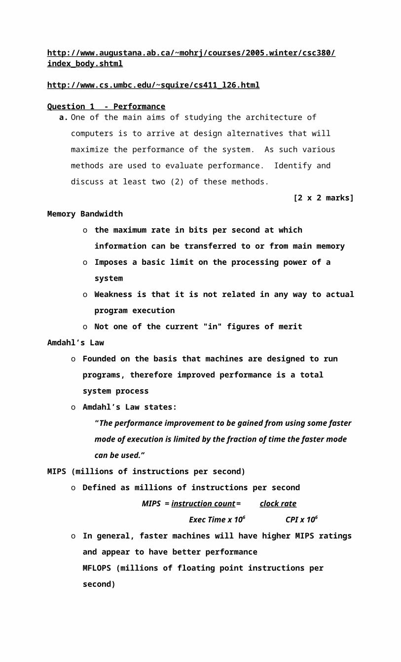
Question 1 - Performancea. One of the main aims of studying the architecture of computers is to arrive at design
alternatives that will maximize the performance of the system. As such various methods
are used to evaluate performance. Identify and discuss at least two (2) of these methods.
[2 x 2 marks]
Memory Bandwidth
o the maximum rate in bits per second at which information can be transferred
to or from main memory
o Imposes a basic limit on the processing power of a system
o Weakness is that it is not related in any way to actual program execution
o Not one of the current "in" figures of merit
Amdahl’s Law
o Founded on the basis that machines are designed to run programs, therefore
improved performance is a total system process
o Amdahl’s Law states:
“The performance improvement to be gained from using some faster mode of
execution is limited by the fraction of time the faster mode can be used.”
MIPS (millions of instructions per second)
o Defined as millions of instructions per second
MIPS = instruction count = clock rate
Exec Time x 106 CPI x 106
o In general, faster machines will have higher MIPS ratings and appear to have
better performance
MFLOPS (millions of floating point instructions per second)
o Useful in comparing performance of "scientific applications“ machines
o Intended to provide a "fair" comparison between such machines since a flop is
the same on all machines
o Problems:
» While a flop is a flop, not all machines implement the same set of flops –
some operations are synthesized from more primitive flops
» MFLOP rating varies with floating point instruction mix -- the idea of fast
vs. slow floating point operations
Benchmarks
o programs specially chosen to accurately measure performance
– Synthetic Benchmarks
– Toy Benchmarks
– Kernels
– Real Programs
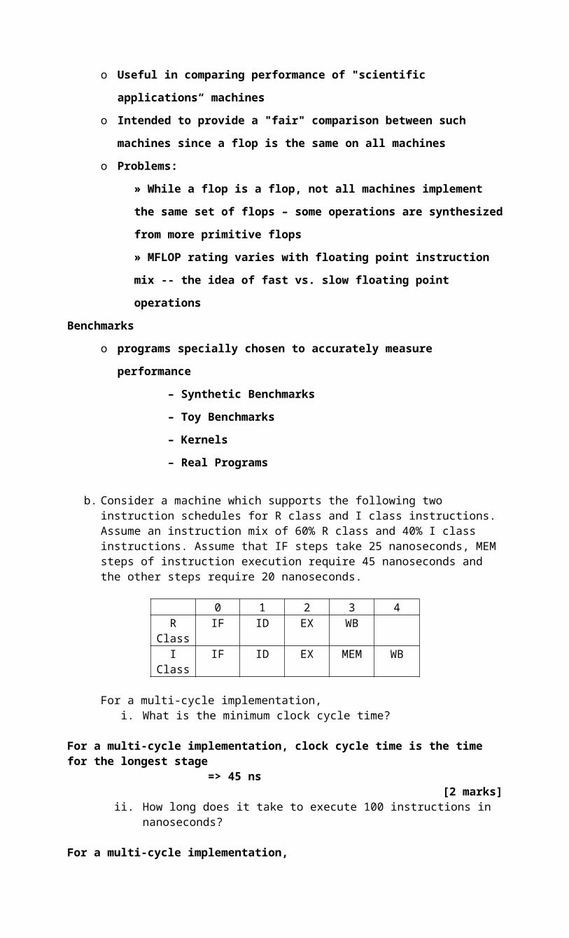
b. Consider a machine which supports the following two instruction schedules for R class and I class instructions. Assume an instruction mix of 60% R class and 40% I class instructions. Assume that IF steps take 25 nanoseconds, MEM steps of instruction execution require 45 nanoseconds and the other steps require 20 nanoseconds.
0 1 2 3 4R Class IF ID EX WBI Class IF ID EX MEM WB
For a multi-cycle implementation,i. What is the minimum clock cycle time?
For a multi-cycle implementation, clock cycle time is the time for the longest stage => 45 ns
[2 marks]ii. How long does it take to execute 100 instructions in nanoseconds?
For a multi-cycle implementation, exec_time = 100 x (exec_time R + exec_time I )
= 100 x (cycle time x CPI x IC) R + (cycle time x CPI x IC) I
= 100 x (4 x 45 x 0.6 + 5 x 45 x 0.4) = 19800ns
[4 marks]
c. Briefly explain the following types of pipeline hazard, indicating how each of them tends to increase the CPI value of a pipelined processor.
i. structural hazardsii. data hazards
iii. control hazards
[3 marks]
Data hazards: Arise when an instruction depends on the results of a previous instruction in a way that is exposed by the overlapping of instructions in the pipeline.
Structural hazards: Arise from resource conflicts when the hardware cannot support all possible combinations of instructions simultaneously in overlapped execution.
Control hazards: Arise from the pipelining of branches and other instructions that change the PC.
d. You have a system that contains a special processor for doing floating-point operations. You have determined that 60% of your computations can use the floating-point processor. When a program uses the floating-point processor, the speedup of the floating-point processor is 40% faster than when it doesn’t use it.
i. What is the overall speedup obtained by using the floating point operations[3 marks]
Overall speedup by using the floating-point processor, where F = 0.6 and S = 1.4= 1
(1 – 0.6) + 0.6/1.4= 1.206
ii. In order to improve the speedup you are considering two options:
Option 1: Modifying the compiler so that 70% of the computations can use the floating-point processor. Cost of this option is $50K.
Option 2: Modifying the floating-point processor. The speedup of the floating-point processor is 100% faster than when it doesn’t use it. Assume in this case that 50% of the computations can use the floating–point processor. Cost of this option is $60K.
Which option would you recommend? Justify your answer quantitatively.[7 marks]
For option 1, F = 0.7 S = 1.4overall speedup
= 1
(1 – 0.7) + 0.7/1.4
= 1.25
Cost/Performance = $50K
1.25
= $40K
For option 2, F = 0.5 S = 2 overall speedup
= 1(1 – 0.5) + 0.5/2
= 1.33
Cost/Performance = $60K
1.33
= $45.1K
Therefore, Option 1 is better because it has a smaller Cost/Speedup ratio.
Question 2a. Argue in favor of or against each of the following statements:
[4 x 2 marks]i. Most computers use direct mapped page tables. (F)
ii. Increasing the block size of a cache is likely to take advantage of temporal locality. (F)
iii. Increasing the page size tends to decrease the size of the page table. (T) iv. Virtual memory typically uses a write-back strategy, rather than a write-
through strategy. (T)
b. For each of the following statements, indicate whether it is true or false, justifying your choice in each case.
[5 x 2 marks]
i. Cache memory serves to provide the CPU fast access to instructions and dataTrue - the cache serves as a buffer between the fast CPU and slow RAM
ii. In a multi-level cache system, the L2 cache may contain data not found in L1.
True - data may be moved from RAM to the L2 cache in blocks; however, only part of those blocks may actually be needed and thus loaded into the L1 cache.
iii. The higher the cache hit-rate, the more likely it is that a larger cache will yield substantial speed-up.False - if the cache hit-rate is already high, it is evident that the current size is adequate. Increasing the cache size will not likely yield substantial improvements in performance.
iv. The L1 cache is typically split into instructions and data for a pipelined system.True - Splitting the L1 cache allows for instruction fetch and operand read/write to occur simultaneously.
v. Increasing the block size of a cache is likely to increase performance primarily because programs exhibit temporal locality. False - Increased block size means that more words are fetched when filling a cache line after a miss on a particular location. If this leads to increased performance, then the nearby words in the block must have been accessed by the program later on, i.e the program is exhibiting spatial locality
c. Given a 100 MHz machine with a with a miss penalty of 20 cycles, a hit time of 2 cycles, and a miss rate of 5%, calculate the average memory access time (AMAT).
[5 marks]
AMAT = hit_time + miss_rate x miss_penalty Since the clock rate is 100 MHz, the cycle time is: 1/(100 MHz) = 10 nswhich gives
AMAT = 10 ns x (2 + 20 x 0.05) = 30 ns
Note: Here we needed to multiply by the cycle time because the hit_time and miss_penalty were given in cycles.
d. Suppose doubling the size of the cache decrease the miss rate to 3%, but causes the hit time to increases to 3 cycles and the miss penalty to increase to 21 cycles. What is the AMAT of the new machine?
[3 marks]
For the new machine: AMAT = 10 ns x (3 + 21 x 0.03) = 36.3 ns
Question 3 (25 marks)
Consider a 16-bit carry look-ahead adder constructed from 4-bit adders with carryLook-ahead logic (2-levels of carry look-ahead).
a. A number of computations, performed by the circuit, are required to obtain the sum and carry from the most significant bit (MSB) of the 16-bit carry look-ahead adder. List these computations in order of their occurrence in hardware. (Hint: You start from producing propagate and generate signals for one-bit adders).
[5marks]
1. Full adders for individual bits compute propagate and generate pi, gi.2. From pi, gi for individual bits Propagate and Generate Pi, Gi for groups of
4 are computed.
3. Pi, Gi for groups of 4 are used to compute Carry-out C1, … , C4 for the groups of 4.
4. Carries for the groups and pi, gi for individual bits are used to compute carries for individual bits c1,…,c15
5. Bits of sum s0,…,s15 are computed from input bits and carries for individual bits by full adders for individual bits
(1 mark each)
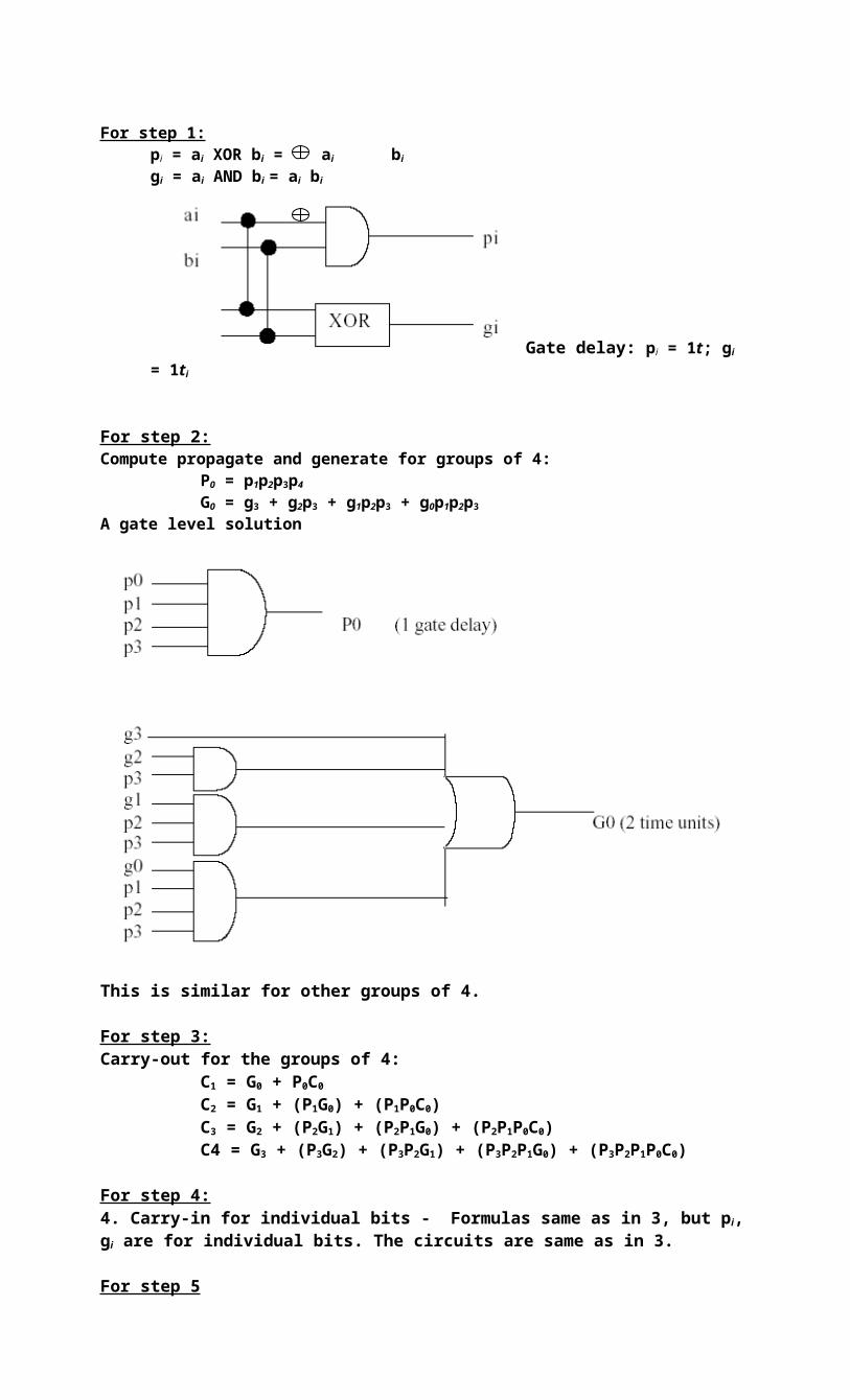
b. For each step of the process given in part a, present formulas and gate-level schematics for hardware executing computations. You don’t need to replicate similar or identical circuits many times but should present samples. Indicate how much time each step takes in terms of gate delay, assuming a 1t delay for each gate.
[10marks]
For step 1:pi = ai XOR bi = ai bi
gi = ai AND bi = ai bi
Gate delay: pi = 1t; gi = 1ti
For step 2:Compute propagate and generate for groups of 4:
P0 = p1p2p3p4
G0 = g3 + g2p3 + g1p2p3 + g0p1p2p3
A gate level solution
This is similar for other groups of 4.
For step 3:Carry-out for the groups of 4:
C1 = G0 + P0C0
C2 = G1 + (P1G0) + (P1P0C0)C3 = G2 + (P2G1) + (P2P1G0) + (P2P1P0C0)
C4 = G3 + (P3G2) + (P3P2G1) + (P3P2P1G0) + (P3P2P1P0C0)
For step 4:4. Carry-in for individual bits - Formulas same as in 3, but pi, gi are for individual bits. The circuits are same as in 3.
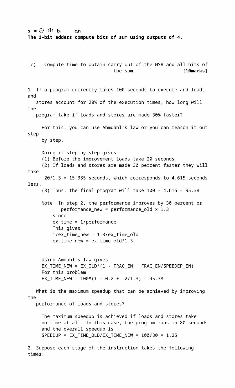
For step 5si = ai bi cinThe 1-bit adders compute bits of sum using outputs of 4.
c) Compute time to obtain carry out of the MSB and all bits of the sum. [10marks]
1. If a program currently takes 100 seconds to execute and loads and stores account for 20% of the execution times, how long will the program take if loads and stores are made 30% faster? For this, you can use Ahmdahl's law or you can reason it out step by step. Doing it step by step gives (1) Before the improvement loads take 20 seconds (2) If loads and stores are made 30 percent faster they will take
20/1.3 = 15.385 seconds, which corresponds to 4.615 seconds less. (3) Thus, the final program will take 100 - 4.615 = 95.38
Note: In step 2, the performance improves by 30 percent or performance_new = performance_old x 1.3 since
ex_time = 1/performance This gives
1/ex_time_new = 1.3/ex_time_old ex_time_new = ex_time_old/1.3
Using Amdahl's law gives EX_TIME_NEW = EX_OLD*(1 - FRAC_EN + FRAC_EN/SPEEDEP_EN)
For this problemEX_TIME_NEW = 100*(1 - 0.2 + .2/1.3) = 95.38
What is the maximum speedup that can be achieved by improving the performance of loads and stores?
The maximum speedup is achieved if loads and stores take no time at all. In this case, the program runs in 80 seconds and the overall speedup is
SPEEDUP = EX_TIME_OLD/EX_TIME_NEW = 100/80 = 1.25
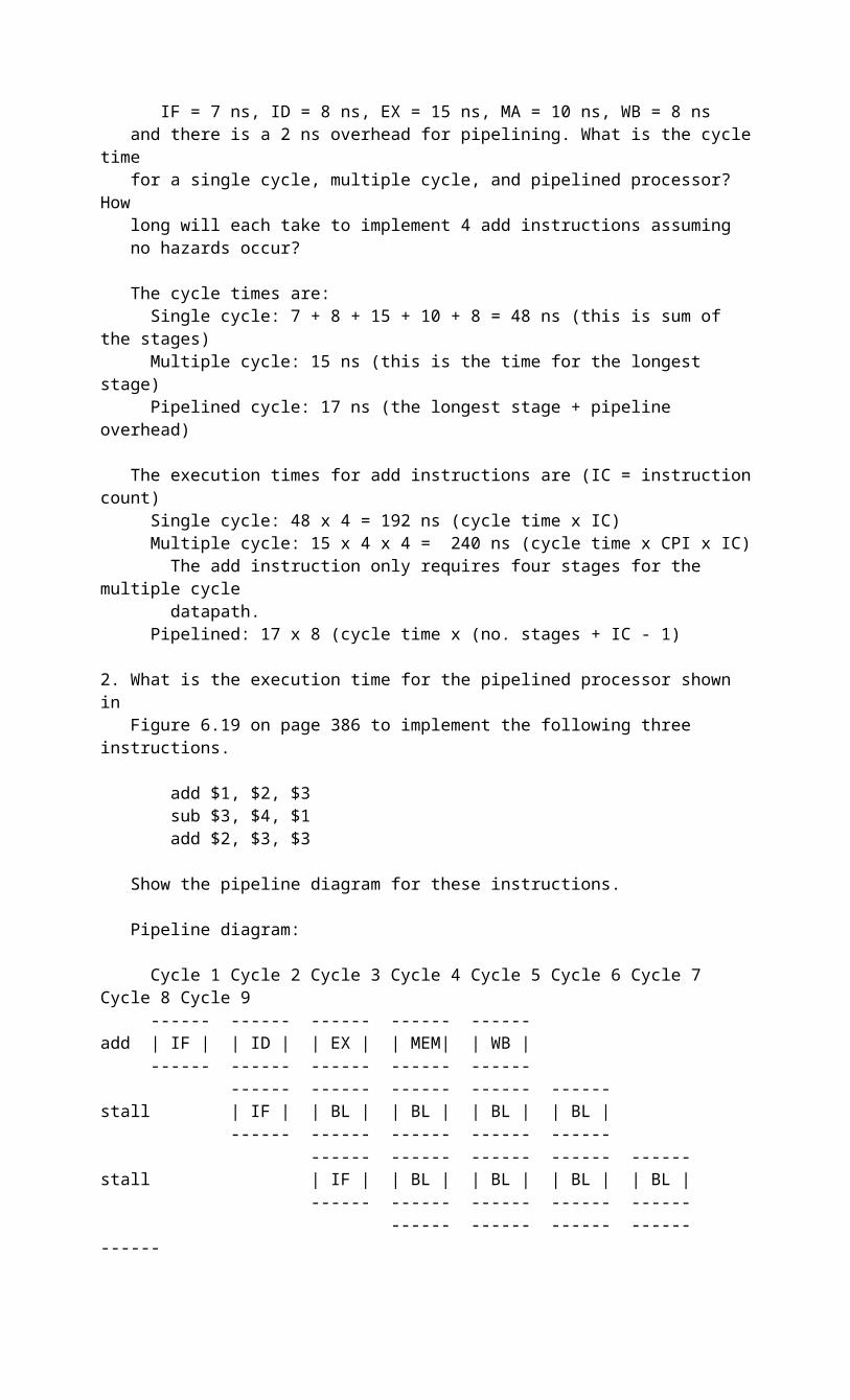
2. Suppose each stage of the instruction takes the following times: IF = 7 ns, ID = 8 ns, EX = 15 ns, MA = 10 ns, WB = 8 ns and there is a 2 ns overhead for pipelining. What is the cycle time for a single cycle, multiple cycle, and pipelined processor? How long will each take to implement 4 add instructions assuming no hazards occur?
The cycle times are: Single cycle: 7 + 8 + 15 + 10 + 8 = 48 ns (this is sum of the stages) Multiple cycle: 15 ns (this is the time for the longest stage) Pipelined cycle: 17 ns (the longest stage + pipeline overhead)
The execution times for add instructions are (IC = instruction count) Single cycle: 48 x 4 = 192 ns (cycle time x IC) Multiple cycle: 15 x 4 x 4 = 240 ns (cycle time x CPI x IC) The add instruction only requires four stages for the multiple cycle datapath. Pipelined: 17 x 8 (cycle time x (no. stages + IC - 1)
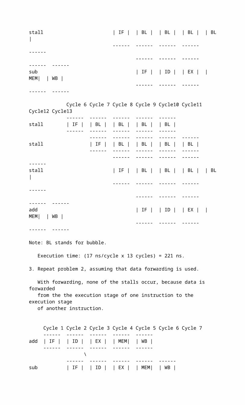
2. What is the execution time for the pipelined processor shown in Figure 6.19 on page 386 to implement the following three instructions.
add $1, $2, $3 sub $3, $4, $1 add $2, $3, $3
Show the pipeline diagram for these instructions.
Pipeline diagram:
Cycle 1 Cycle 2 Cycle 3 Cycle 4 Cycle 5 Cycle 6 Cycle 7 Cycle 8 Cycle 9 ------ ------ ------ ------ ------add | IF | | ID | | EX | | MEM| | WB | ------ ------ ------ ------ ------ ------ ------ ------ ------ ------ stall | IF | | BL | | BL | | BL | | BL | ------ ------ ------ ------ ------ ------ ------ ------ ------ ------ stall | IF | | BL | | BL | | BL | | BL | ------ ------ ------ ------ ------ ------ ------ ------ ------ ------ stall | IF | | BL | | BL | | BL | | BL | ------ ------ ------ ------ ------ ------ ------ ------ ------ ------sub | IF | | ID | | EX | | MEM| | WB | ------ ------ ------ ------ ------ Cycle 6 Cycle 7 Cycle 8 Cycle 9 Cycle10 Cycle11 Cycle12 Cycle13 ------ ------ ------ ------ ------ stall | IF | | BL | | BL | | BL | | BL | ------ ------ ------ ------ ------ ------ ------ ------ ------ ------ stall | IF | | BL | | BL | | BL | | BL | ------ ------ ------ ------ ------ ------ ------ ------ ------ ------ stall | IF | | BL | | BL | | BL | | BL | ------ ------ ------ ------ ------ ------ ------ ------ ------ ------add | IF | | ID | | EX | | MEM| | WB | ------ ------ ------ ------ ------
Note: BL stands for bubble.
Execution time: (17 ns/cycle x 13 cycles) = 221 ns.
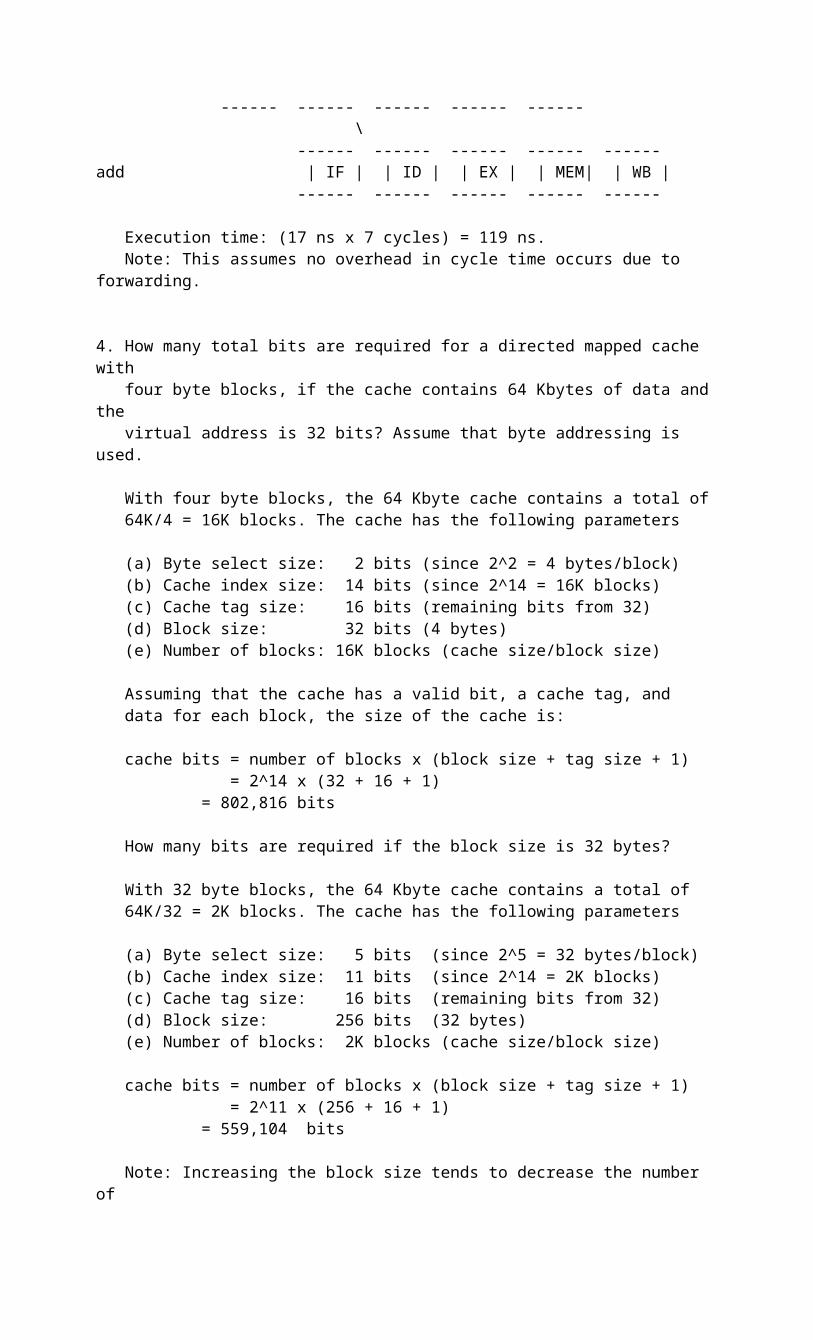
3. Repeat problem 2, assuming that data forwarding is used.
With forwarding, none of the stalls occur, because data is forwarded from the the execution stage of one instruction to the execution stage of another instruction.
Cycle 1 Cycle 2 Cycle 3 Cycle 4 Cycle 5 Cycle 6 Cycle 7
------ ------ ------ ------ ------add | IF | | ID | | EX | | MEM| | WB | ------ ------ ------ ------ ------
\ ------ ------ ------ ------ ------ sub | IF | | ID | | EX | | MEM| | WB | ------ ------ ------ ------ ------
\ ------ ------ ------ ------ ------ add | IF | | ID | | EX | | MEM| | WB | ------ ------ ------ ------ ------
Execution time: (17 ns x 7 cycles) = 119 ns. Note: This assumes no overhead in cycle time occurs due to forwarding.
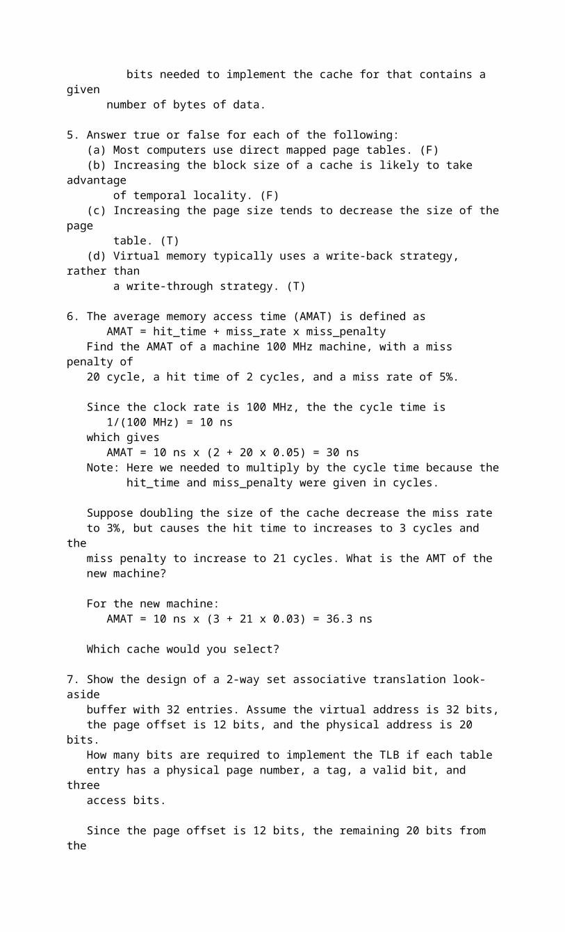
4. How many total bits are required for a directed mapped cache with four byte blocks, if the cache contains 64 Kbytes of data and the virtual address is 32 bits? Assume that byte addressing is used. With four byte blocks, the 64 Kbyte cache contains a total of 64K/4 = 16K blocks. The cache has the following parameters
(a) Byte select size: 2 bits (since 2^2 = 4 bytes/block) (b) Cache index size: 14 bits (since 2^14 = 16K blocks) (c) Cache tag size: 16 bits (remaining bits from 32) (d) Block size: 32 bits (4 bytes) (e) Number of blocks: 16K blocks (cache size/block size)
Assuming that the cache has a valid bit, a cache tag, and data for each block, the size of the cache is:
cache bits = number of blocks x (block size + tag size + 1) = 2^14 x (32 + 16 + 1)
= 802,816 bits
How many bits are required if the block size is 32 bytes?
With 32 byte blocks, the 64 Kbyte cache contains a total of 64K/32 = 2K blocks. The cache has the following parameters
(a) Byte select size: 5 bits (since 2^5 = 32 bytes/block) (b) Cache index size: 11 bits (since 2^14 = 2K blocks) (c) Cache tag size: 16 bits (remaining bits from 32) (d) Block size: 256 bits (32 bytes) (e) Number of blocks: 2K blocks (cache size/block size)
cache bits = number of blocks x (block size + tag size + 1) = 2^11 x (256 + 16 + 1)
= 559,104 bits
Note: Increasing the block size tends to decrease the number of bits needed to implement the cache for that contains a given
number of bytes of data. 5. Answer true or false for each of the following: (a) Most computers use direct mapped page tables. (F) (b) Increasing the block size of a cache is likely to take advantage of temporal locality. (F) (c) Increasing the page size tends to decrease the size of the page table. (T) (d) Virtual memory typically uses a write-back strategy, rather than
a write-through strategy. (T)
6. The average memory access time (AMAT) is defined as AMAT = hit_time + miss_rate x miss_penalty Find the AMAT of a machine 100 MHz machine, with a miss penalty of 20 cycle, a hit time of 2 cycles, and a miss rate of 5%. Since the clock rate is 100 MHz, the the cycle time is 1/(100 MHz) = 10 ns which gives AMAT = 10 ns x (2 + 20 x 0.05) = 30 ns Note: Here we needed to multiply by the cycle time because the hit_time and miss_penalty were given in cycles. Suppose doubling the size of the cache decrease the miss rate to 3%, but causes the hit time to increases to 3 cycles and the miss penalty to increase to 21 cycles. What is the AMT of the new machine?
For the new machine: AMAT = 10 ns x (3 + 21 x 0.03) = 36.3 ns
Which cache would you select?
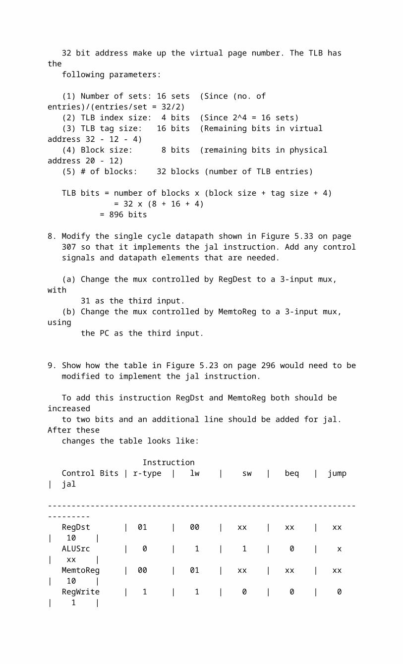
7. Show the design of a 2-way set associative translation look-aside buffer with 32 entries. Assume the virtual address is 32 bits, the page offset is 12 bits, and the physical address is 20 bits. How many bits are required to implement the TLB if each table entry has a physical page number, a tag, a valid bit, and three access bits.
Since the page offset is 12 bits, the remaining 20 bits from the 32 bit address make up the virtual page number. The TLB has the following parameters: (1) Number of sets: 16 sets (Since (no. of entries)/(entries/set = 32/2) (2) TLB index size: 4 bits (Since 2^4 = 16 sets) (3) TLB tag size: 16 bits (Remaining bits in virtual address 32 - 12 - 4) (4) Block size: 8 bits (remaining bits in physical address 20 - 12) (5) # of blocks: 32 blocks (number of TLB entries)
TLB bits = number of blocks x (block size + tag size + 4) = 32 x (8 + 16 + 4)
= 896 bits 8. Modify the single cycle datapath shown in Figure 5.33 on page 307 so that it implements the jal instruction. Add any control signals and datapath elements that are needed.
(a) Change the mux controlled by RegDest to a 3-input mux, with 31 as the third input. (b) Change the mux controlled by MemtoReg to a 3-input mux, using the PC as the third input.
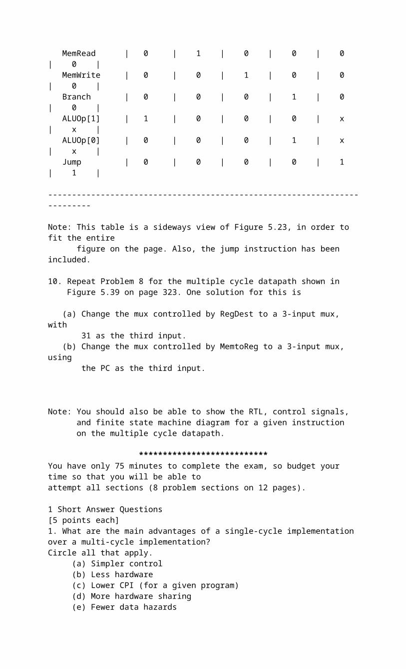
9. Show how the table in Figure 5.23 on page 296 would need to be modified to implement the jal instruction.
To add this instruction RegDst and MemtoReg both should be increased to two bits and an additional line should be added for jal. After these changes the table looks like:
Instruction Control Bits | r-type | lw | sw | beq | jump | jal -------------------------------------------------------------------------- RegDst | 01 | 00 | xx | xx | xx | 10 | ALUSrc | 0 | 1 | 1 | 0 | x | xx | MemtoReg | 00 | 01 | xx | xx | xx | 10 | RegWrite | 1 | 1 | 0 | 0 | 0 | 1 | MemRead | 0 | 1 | 0 | 0 | 0 | 0 | MemWrite | 0 | 0 | 1 | 0 | 0 | 0 | Branch | 0 | 0 | 0 | 1 | 0 | 0 | ALUOp[1] | 1 | 0 | 0 | 0 | x | x | ALUOp[0] | 0 | 0 | 0 | 1 | x | x | Jump | 0 | 0 | 0 | 0 | 1 | 1 | --------------------------------------------------------------------------
Note: This table is a sideways view of Figure 5.23, in order to fit the entire figure on the page. Also, the jump instruction has been included.
10. Repeat Problem 8 for the multiple cycle datapath shown in Figure 5.39 on page 323. One solution for this is
(a) Change the mux controlled by RegDest to a 3-input mux, with 31 as the third input. (b) Change the mux controlled by MemtoReg to a 3-input mux, using the PC as the third input.
Note: You should also be able to show the RTL, control signals, and finite state machine diagram for a given instruction on the multiple cycle datapath.
***************************You have only 75 minutes to complete the exam, so budget your time so that you will be able toattempt all sections (8 problem sections on 12 pages).
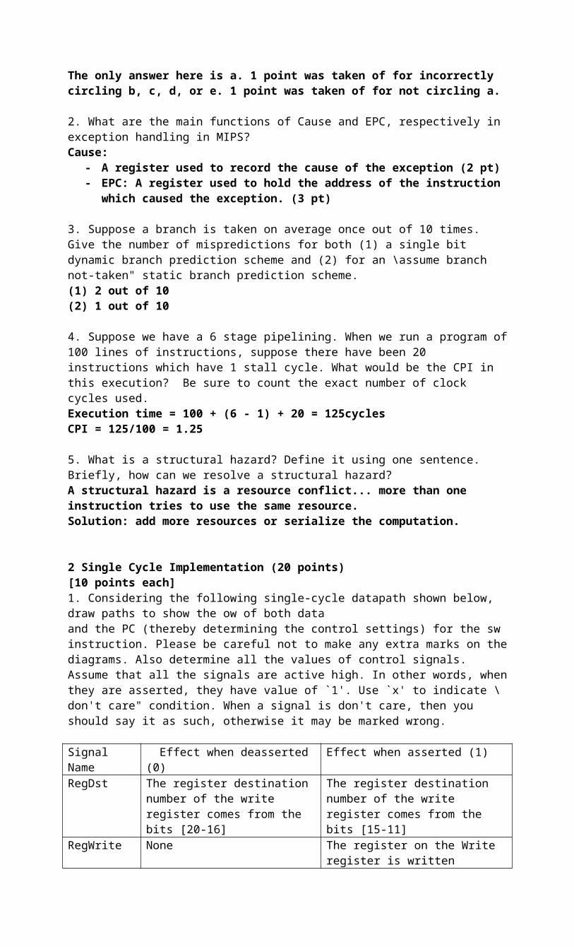
1 Short Answer Questions[5 points each]1. What are the main advantages of a single-cycle implementation over a multi-cycle implementation?Circle all that apply.
(a) Simpler control(b) Less hardware(c) Lower CPI (for a given program)(d) More hardware sharing(e) Fewer data hazards
The only answer here is a. 1 point was taken of for incorrectly circling b, c, d, or e. 1 point was taken of for not circling a.
2. What are the main functions of Cause and EPC, respectively in exception handling in MIPS? Cause:
- A register used to record the cause of the exception (2 pt)- EPC: A register used to hold the address of the instruction which caused the
exception. (3 pt)
3. Suppose a branch is taken on average once out of 10 times. Give the number of mispredictions for both (1) a single bit dynamic branch prediction scheme and (2) for an \assume branch not-taken" static branch prediction scheme.(1) 2 out of 10(2) 1 out of 10
4. Suppose we have a 6 stage pipelining. When we run a program of 100 lines of instructions, suppose there have been 20 instructions which have 1 stall cycle. What would be the CPI in this execution? Be sure to count the exact number of clock cycles used.Execution time = 100 + (6 - 1) + 20 = 125cyclesCPI = 125/100 = 1.25
5. What is a structural hazard? Define it using one sentence. Briefly, how can we resolve a structural hazard?A structural hazard is a resource conflict... more than one instruction tries to use the same resource.Solution: add more resources or serialize the computation.
2 Single Cycle Implementation (20 points)[10 points each]1. Considering the following single-cycle datapath shown below, draw paths to show the ow of both dataand the PC (thereby determining the control settings) for the sw instruction. Please be careful not to make any extra marks on the diagrams. Also determine all the values of control signals. Assume that all the signals are active high. In other words, when they are asserted, they have value of `1'. Use `x' to indicate \don't care" condition. When a signal is don't care, then you should say it as such, otherwise it may be marked wrong.
Signal Name Effect when deasserted (0) Effect when asserted (1)RegDst The register destination number of
the write register comes from the bits [20-16]
The register destination number of the write register comes from the bits [15-11]
RegWrite None The register on the Write register is written
ALUSrc Select the second input Select the first inputPCSrc Select the second input Select the first inputMemRead None Data memory contents designated by
the addr are put on the Read data.MemWrite None Data memory contents designated by
the addr are replaced by the value on the Write data.
MemToReg Select the second data Select the first dataBranch The instruction is not a branch The instruction is a branch.
sw $8, 1234($7)
Pipelining http://6004.csail.mit.edu/Fall01/
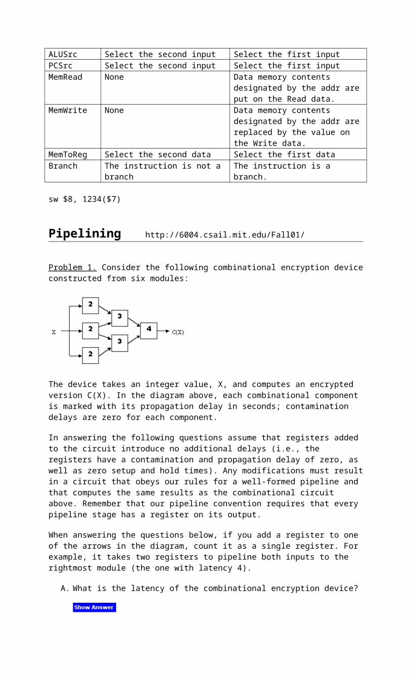
Problem 1. Consider the following combinational encryption device constructed from six modules:
The device takes an integer value, X, and computes an encrypted version C(X). In the diagram above, each combinational component is marked with its propagation delay in seconds; contamination delays are zero for each component.
In answering the following questions assume that registers added to the circuit introduce no additional delays (i.e., the registers have a contamination and propagation delay of zero, as well as zero setup and hold times). Any modifications must result in a circuit that obeys our rules for a well-formed pipeline and that computes the same results as the combinational circuit above. Remember that our pipeline convention requires that every pipeline stage has a register on its output.
When answering the questions below, if you add a register to one of the arrows in the diagram, count it as a single register. For example, it takes two registers to pipeline both inputs to the rightmost module (the one with latency 4).
A. What is the latency of the combinational encryption device?
Latency = delay along longest path from input to output = 2 + 3 + 4 = 9. B. If we want to increase the throughput of the encryption device, what is the minimum
number of registers we need to add?
Three. Playing by our pipelining rules, we always add a register to the output. The increase the throughput we need to add other register that bisect the circuit. The cheapest place to do this is just before the "4" module, requiring two additional registers.
C. If we are required to add exactly 5 registers, what is the best throughput we can achieve?
The best throughput we can achieve with 5 registers is 1/5: place 3 (!) registers on the output and two registers on the arcs leading to the "4" module. If we use 4 registers to divide the circuit between the "2" and "3" modules, the resulting throughput is 1/7.
D. If we can add as many registers as we like, is there an upper bound on the throughput we can achieve?
Yes: 1/4, because the best we can do by just adding registers is to segregate the "4" module into its own pipeline stage.
E. If we can add as many registers as we like, is there a lower bound on the latency we can achieve?
Lower bound on latency = 9. We can never make the latency less by adding pipeline registers; usually the latency increases.
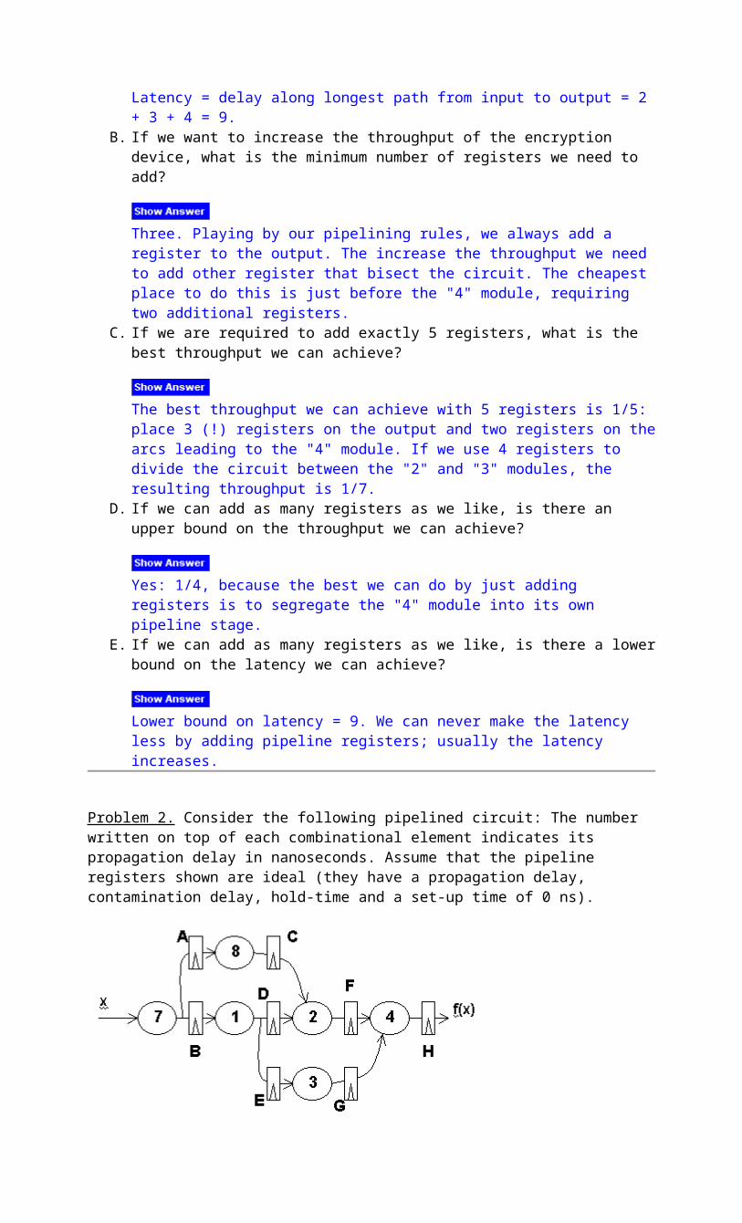
Problem 2. Consider the following pipelined circuit: The number written on top of each combinational element indicates its propagation delay in nanoseconds. Assume that the pipeline registers shown are ideal (they have a propagation delay, contamination delay, hold-time and a set-up time of 0 ns).
A. What is the minimum clock period for which we can expect the given circuit to operate correctly?
8ns since we have to leave time for the logic between registers A and C to do its stuff. B. What is the minimum latency of the circuit as shown?
32ns = 4 pipeline stages at 8ns clock period. C. If the registers labeled F and G are removed, describe the resulting circuit's behavior.
Removing F and G combines the last two pipeline stages into a single pipeline stage. The latency improves to 24ns and the throughput stays 1/8ns.
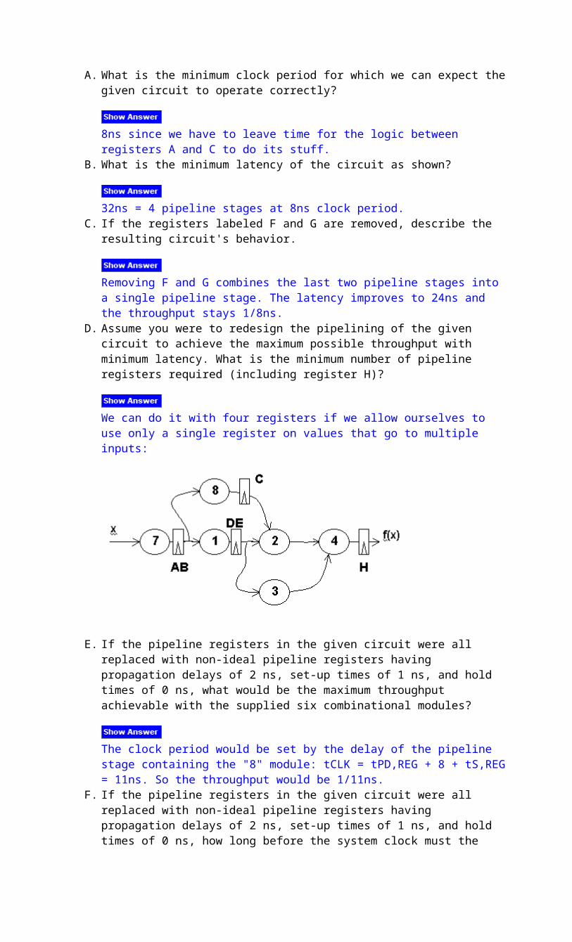
D. Assume you were to redesign the pipelining of the given circuit to achieve the maximum possible throughput with minimum latency. What is the minimum number of pipeline registers required (including register H)?
We can do it with four registers if we allow ourselves to use only a single register on values that go to multiple inputs:
E. If the pipeline registers in the given circuit were all replaced with non-ideal pipeline registers having propagation delays of 2 ns, set-up times of 1 ns, and hold times of 0 ns, what would be the maximum throughput achievable with the supplied six combinational modules?
The clock period would be set by the delay of the pipeline stage containing the "8" module: tCLK = tPD,REG + 8 + tS,REG = 11ns. So the throughput would be 1/11ns.
F. If the pipeline registers in the given circuit were all replaced with non-ideal pipeline registers having propagation delays of 2 ns, set-up times of 1 ns, and hold times of 0 ns, how long before the system clock must the input x be set-up to assure that the pipeline registers A and B do not go into a metastable state?
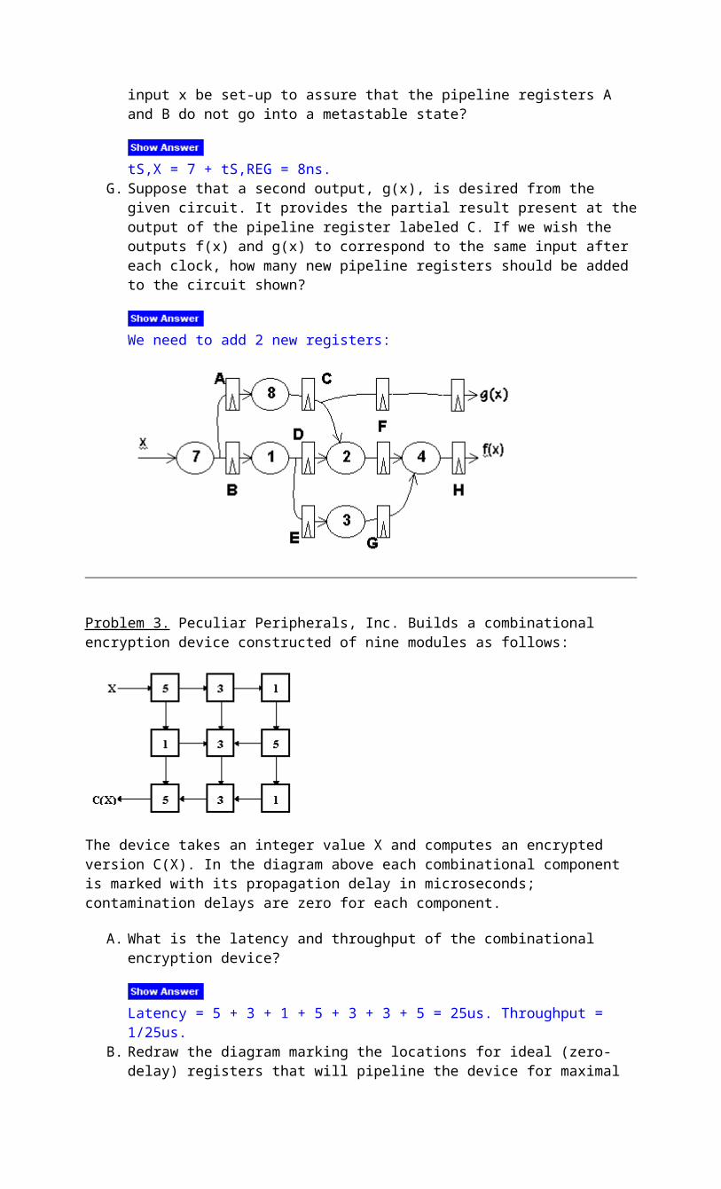
tS,X = 7 + tS,REG = 8ns. G. Suppose that a second output, g(x), is desired from the given circuit. It provides the
partial result present at the output of the pipeline register labeled C. If we wish the outputs f(x) and g(x) to correspond to the same input after each clock, how many new pipeline registers should be added to the circuit shown?
We need to add 2 new registers:
Problem 3. Peculiar Peripherals, Inc. Builds a combinational encryption device constructed of nine modules as follows:
The device takes an integer value X and computes an encrypted version C(X). In the diagram above each combinational component is marked with its propagation delay in microseconds; contamination delays are zero for each component.
A. What is the latency and throughput of the combinational encryption device?
Latency = 5 + 3 + 1 + 5 + 3 + 3 + 5 = 25us. Throughput = 1/25us. B. Redraw the diagram marking the locations for ideal (zero-delay) registers that will
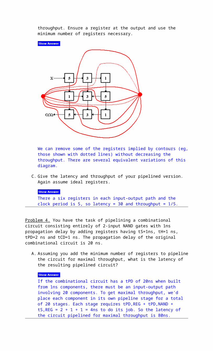
pipeline the device for maximal throughput. Ensure a register at the output and use the minimum number of registers necessary.
We can remove some of the registers implied by contours (eg, those shown with dotted lines) without decreasing the throughput. There are several equivalent variations of this diagram.
C. Give the latency and throughput of your pipelined version. Again assume ideal registers.
There a six registers in each input-output path and the clock period is 5, so latency = 30 and throughput = 1/5.
Problem 4. You have the task of pipelining a combinational circuit consisting entirely of 2-input NAND gates with 1ns propagation delay by adding registers having tS=1ns, tH=1 ns, tPD=2 ns and tCD=1 ns. The propagation delay of the original combinational circuit is 20 ns.
A. Assuming you add the minimum number of registers to pipeline the circuit for maximal throughput, what is the latency of the resulting pipelined circuit?
If the combinational circuit has a tPD of 20ns when built from 1ns components, there must be an input-output path involving 20 components. To get maximal throughput, we'd place each component in its own pipeline stage for a total of 20 stages. Each stage requires tPD,REG + tPD,NAND + tS,REG = 2 + 1 + 1 = 4ns to do its job. So the latency of the circuit pipelined for maximal throughput is 80ns.
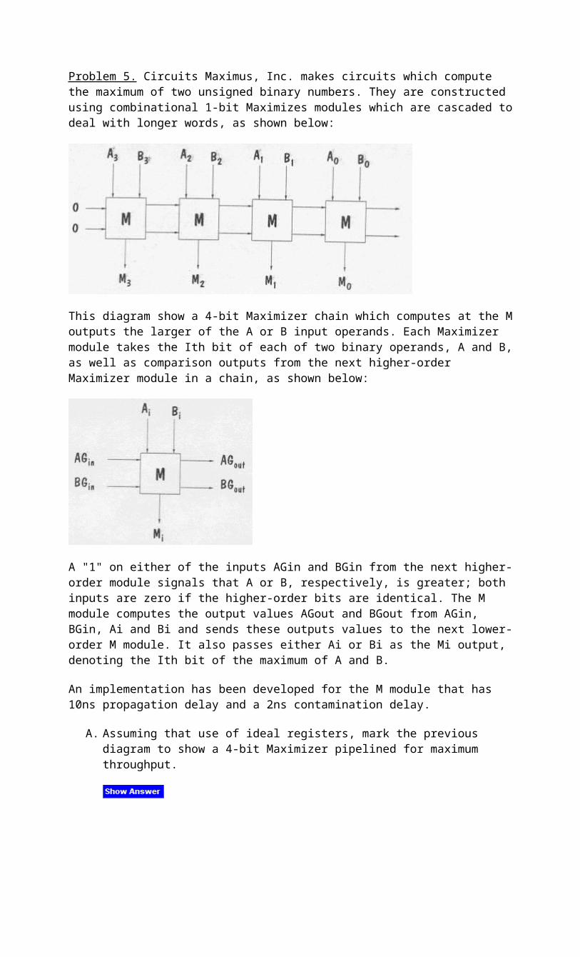
Problem 5. Circuits Maximus, Inc. makes circuits which compute the maximum of two unsigned binary numbers. They are constructed using combinational 1-bit Maximizes modules which are cascaded to deal with longer words, as shown below:
This diagram show a 4-bit Maximizer chain which computes at the M outputs the larger of the A or B input operands. Each Maximizer module takes the Ith bit of each of two binary operands, A and B, as well as comparison outputs from the next higher-order Maximizer module in a chain, as shown below:
A "1" on either of the inputs AGin and BGin from the next higher-order module signals that A or B, respectively, is greater; both inputs are zero if the higher-order bits are identical. The M
module computes the output values AGout and BGout from AGin, BGin, Ai and Bi and sends these outputs values to the next lower-order M module. It also passes either Ai or Bi as the Mi output, denoting the Ith bit of the maximum of A and B.
An implementation has been developed for the M module that has 10ns propagation delay and a 2ns contamination delay.
A. Assuming that use of ideal registers, mark the previous diagram to show a 4-bit Maximizer pipelined for maximum throughput.
B. To compute the maximum value of N inputs (N > 2), the following structure is proposed:
In this circuit, the maximum of four 4-bit unsigned numbers is computed and appears at the output M3..M0. What is the latency and throughput of this combinational circuit, assuming that each M module has a propagation delay of 10ns?
The longest path from inputs to outputs passes through 6 M modules, so the latency is 60 and the throughput is 1/60.
C. Show how this circuit can be pipelined from maximum throughput using a minimum number of pipeline stages. Remember to include a register at each output.
The solution below uses a different technique for pipelining a circuit. Start by labeling each module with its maximum "distance" from the inputs, i.e., the largest number of components that have to be traversed on some path from the inputs to the module in question. Label all outputs with the length (in modules) of the longest path from input to output label each input with "0". The number of pipeline registers required on each wire is the difference between the label at the start of the arrow and the end of the arrow.
A common mistake: forgetting to add the necessary pipeline registers on the input and output arrows.
Problem 6. The following combinational circuit takes a single input and produces a visual output by lighting the light on the center component module.
Consider the result of pipelining the above circuit for maximum throughput, using the minimum number of registers necessary. The result would be a pipeline such that input asserted during
clock period I produces the proper output on the light during clock period I+K (we want minimal K which gives maximal throughput).
A. How many registers should appear on the bold wire (marked X) in the pipelined version of the above circuit?
Using the pipelining technique described in the previous problem, we can see from the labels that 7 registers would be required on the wire marked X:
Problem 7. Partial Products, Inc., has hired you as its vice president in charge of marketing. Your immediate task is to determine the sale prices of three newly announced multiplier modules. The top-of-the-line Cooker is a pipelined multiplier. The Sizzler is a combinational multiplier. The Grunter is a slower sequential multiplier. Their performance figures are as follows (T is some constant time interval):
Throughput LatencyCooker 1/T 5TSizzler 1/4T 4TGrunter 1/32T 32T
Customers follow a single principle: Buy the cheapest combination of hardware that meets my performance requirements. These requirements may be specified as a maximum allowable latency time, a minimum acceptable throughput, or some combination of these. Customers are willing to try any paralleled or pipelined configuration of multipliers in an attempt to achieve the requisite performance. You may neglect the cost (both financial and as a decrease in performance) of any routing, latching, or other hardware needed to construct a configuration. Concentrate only on the inherent capabilities of the arrangement of multipliers itself.
It has been decided that the Cooker will sell for $1000. The following questions deal with determining the selling prices of Sizzlers and Grunters.
A. How much can you charge for Sizzlers and still sell any? That is, is there some price for Sizzlers above which any performance demands that could be met by a Sizzler could also be met by some combination of Cookers costing less? If there is no such maximum price, indicate a performance requirement that could be met by a Sizzler but not by any combination of Cookers. If there is a maximum selling price, give the price and explain your reasoning.
If there is a performance requirement for the latency to be <= 4T, then there is no combination of Cookers that will meet this performance requirement. So it is in theory possible to sell some Sizzlers at any price. Using multiple Cookers can further improve the overall multiplier throughput, but their latency cannot be shortened.
B. How little can you charge for Sizzlers and still sell any Cookers? In other words, is there a price for the Sizzler below which every customer would prefer to buy Sizzlers rather than a Cooker? Give and explain your answer, as above.
The minimum price for a Sizzler is $250.01 if we want to continue to sell Cookers. If the price of a Sizzler is less than that, 4 Sizzlers could be used in parallel to achieve the same throughput as a Cooker with a better latency in the bargain.
C. Is there a maximum price for the Grunter above which every customer would prefer to buy Cookers instead? As before, give the price, if it exists, and explain your reasoning in either case.
The maximum price for the Grunter is $999.99 since for applications that can accept long latencies (>= 32T) it's worth buying a Grunter if it saves any money at all.
D. Is there a minimum price for the Grunter below which every customer would prefer to buy Grunters rather than a Cooker? Once again, give the price, if it exists, and explain your reasoning in either case.
There is no minimum price for a Grunter that would cause every customer to buy Grunters instead of Cookers. The latency of the Grunter will always be 32T, so when performance requirements demand latencies < 32T, Grunters won't do the job.
E. Suppose that, as a customer, you have an application in which 64 pairs of numbers appear all at once, and their 64 products must be generated in as short a time as practicable. You have $1000 to spend. At what price would you consider using Sizzlers? At what price would you consider using Grunters?
Sizzlers will be considered when they cost $250 or less. Grunters may be considered when they cost $124.93 or less. To see this, consider the case when Sizzlers cost $125.01. Buying seven Sizzlers would yield a latency of 40T at a cost of $875.07. The customer cannot afford another Sizzler, but adding a single Grunter for $124.93 will reduce the latency to 36T. All optimal configurations are explored below:
Caches [Printable PDF version]
Problem 1.
The diagram above illustrates a blocked, direct-mapped cache for a computer that uses 32-bit data words and 32-bit byte addresses.
A. What is the maximum number words of data from main memory that can be stored in the cache at any one time?
Maximum number of data words from main memory = (16 lines)(4 words/line) = 64 words
B. How many bits of the address are used to select which line of the cache is accessed?
With 16 cache lines, 4 bits of the address are required to select which line of the cache is accessed.
C. How many bits wide is the tag field?
Bits in the tag field = (32 address bits) - (4 bits to select line) - (4 bits to select word/byte) = 24 bits
D. Briefly explain the purpose of the one-bit V field associated with each cache line.
The tag and data fields of the cache will always have value in them, so the V bit is used to denote whether these value are consistent (valid) with what is in memory. Typically the V bit for each line in the cache is set to "0" when the machine is reset or the cache is flushed.
E. Assume that memory location 0x2045C was present in the cache. Using the row and column labels from the figure, in what cache location(s) could we find the data from that memory location? What would the value(s) of the tag field(s) have to be for the cache row(s) in which the data appears?
The cache uses ADDR[7:4] to determine where data from a particular address will be stored in the cache. Thus, location 0x0002045C will be stored in line 5 of cache. The tag field should contain the upper 24 bits of the address, i.e., 0x000204. Note that the bottom 4 bits of the address (0xC) determine which word and byte of the cache line is being referenced.
F. Can data from locations 0x12368 and 0x322FF8 be present in the cache at the same time? What about data from locations 0x2536038 and 0x1034? Explain.
Location 0x12368 will be stored in line 6 of the cache. Location 0x322F68 will be stored in line F of the cache. Since the lines differ, both locations can be cached at the same time. However, locations 0x2536038 and 0x1034 both would be stored in line 3 of cache, so they both could not be present in the cache at the same time.
G. When an access causes a cache miss, how many words need to be fetched from memory to fill the appropriate cache location(s) and satisfy the request?
There are 4 words in each line of the cache and since we only have one valid bit for the whole line, all 4 words have to have valid values. So to fill a cache line on a cache miss all 4 words would have to be fetched from main memory.
Problem 2. Cache multiple choice:
A. If a cache access requires one clock cycle and handling cache misses stalls the processor for an additional five cycles, which of the following cache hit rates comes closest to achieving an average memory access of 2 cycles?
(A) 75%(B) 80%(C) 83%(D) 86%(E) 98%
2 cycle average access = (1 cycle for cache) + (1 - hit rate)(5 cycles stall)=> hit rate = 80%
B. LRU is an effective cache replacement strategy primarily because programs
(A) exhibit spatial locality(B) exhibit temporal locality(C) usually have small working sets(D) read data much more frequently than write data(E) can generate addresses that collide in the cache
(B). Temporal locality implies that the probability of accessing a location decreases as the time since the last access increases. By choosing to replace locations that haven't been used for the longest time, the least-recently-used replacement strategy should, in theory, be replacing locations that have the lowest probability of being accessed in the future.
C. If increasing the associativity of a cache improves performance it is primarily because programs
(A) exhibit spatial locality(B) exhibit temporal locality(C) usually have small working sets(D) read data much more frequently than write data(E) can generate addresses that collide in the cache
(E). Increasing cache associativity means that there are more cache locations in which a given memory word can reside, so replacements due to cache collisions (multiple addresses mapping to the same cache location) should be reduced.
D. If increasing the block size of a cache improves performance it is primarily because programs
(A) exhibit spatial locality(B) exhibit temporal locality(C) usually have small working sets(D) read data much more frequently than write data(E) can generate addresses that collide in the cache
(A). Increased block size means that more words are fetched when filling a cache line after a miss on a particular location. If this leads to increased performance, then the nearby words in the block must have been accessed by the program later on, ie, the program is exhibiting spatial locality.
E. A fully-associative cache using an LRU replacement policy always has a better hit rate than a direct-mapped cache with the same total data capacity.
(A) true(B) false
False. Suppose both caches contain N words and consider a program that repeatedly accesses locations 0 through N (a total of N+1 words). The direct-mapped cache will map locations 0 and N into the same cache line and words 1 through N-1 into separate cache lines. So in the steady state, the program will miss twice (on locations 0 and N) each time through the loop.
Now the fully-associative case: when the program first accesses word N, the FA cache will replace word 0 (the least-recently-used location). The next access is to location 0 and the FA cache will replace word 1, etc. So the FA cache is always choosing the replace the word the program is about to access, leading to a 0% hit rate!
F. Consider the following program:
G. integer A[1000];H. for i = 1 to 1000I. for j = 1 to 1000J. A[i] = A[i] + 1
When the above program is compiled with all compiler optimizations turned off and run on a processor with a 1K byte direct-mapped write-back data cache with 4-word cache blocks, what is the approximate data cache miss rate? (Assume integers are one word long and a word is 4 bytes.)
(A) 0.0125%(B) 0.05%(C) 0.1%(D) 5%(E) 12.5%
(A). Considering only the data accesses, the program performs 1,000,000 reads and 1,000,000 writes. Since the cache has 4-word blocks, each miss brings 4 words of the array into the cache. So accesses to the next 3 array locations won't cause a miss. Since the cache is write-back, writes happen directly into the cache without causing any memory accesses until the word is replaced. So altogether there are 250 misses (caused by a read of A[0], A[4], A[8], ...), for a miss rate of 250/2,000,000 = 0.0125%
G. In a non-pipelined single-cycle-per-instruction processor with an instruction cache, the average instruction cache miss rate is 5%. It takes 8 clock cycles to fetch a cache line from the main memory. Disregarding data cache misses, what is the approximate average CPI (cycles per instruction)?
(A) 0.45(B) 0.714(C) 1.4(D) 1.8(E) 2.22
(C). CPI = (1 inst-per-cycle) + (0.05)(8 cycles/miss) = 1.4 H. Consider an 8-line one-word-block direct-mapped cache initialized to all zeroes where
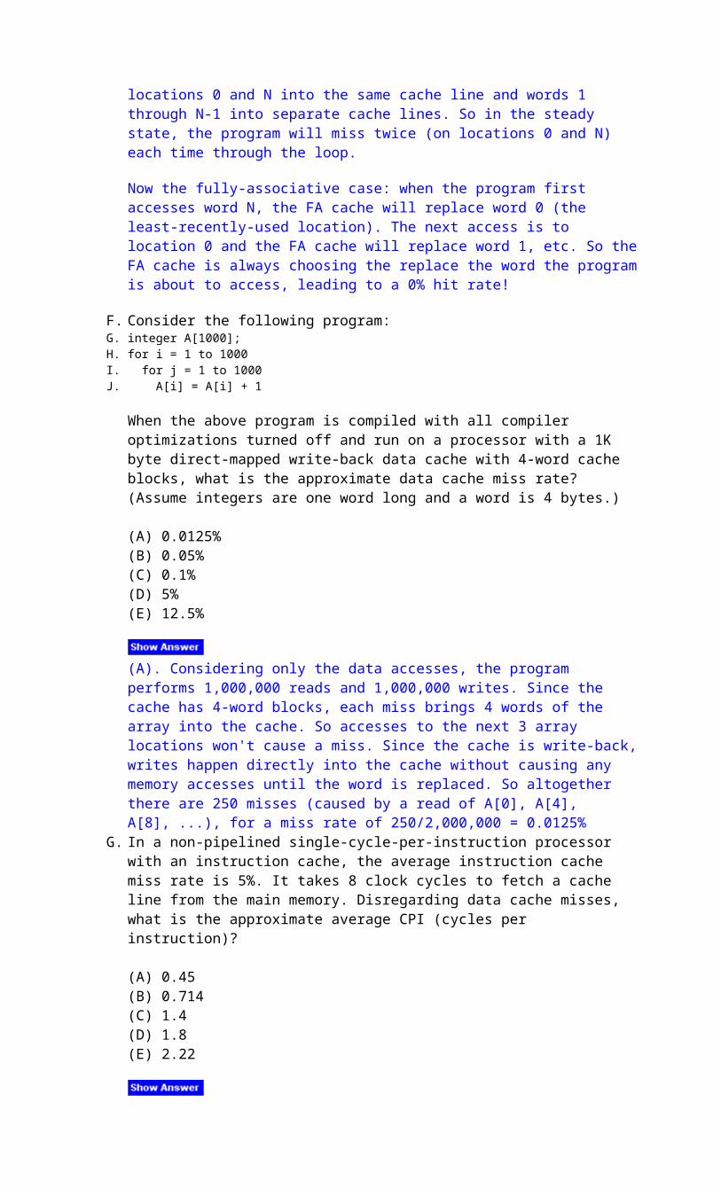
the following sequence of word addresses are accessed:
1, 4, 5, 20, 9, 19, 4, 5, 6, and 9.
Which of the following tables reflect the final tag bits of the cache?
First map the addresses to cache line numbers and tags where line number = address mod 8tag = floor(address / 8)
address: 1 4 5 20 9 19 4 5 6 9line #: 1 4 5 4 1 3 4 5 6 1tag: 0 0 0 2 1 2 0 0 0 1
So, figure (E) represents the final tag bits of the cache.
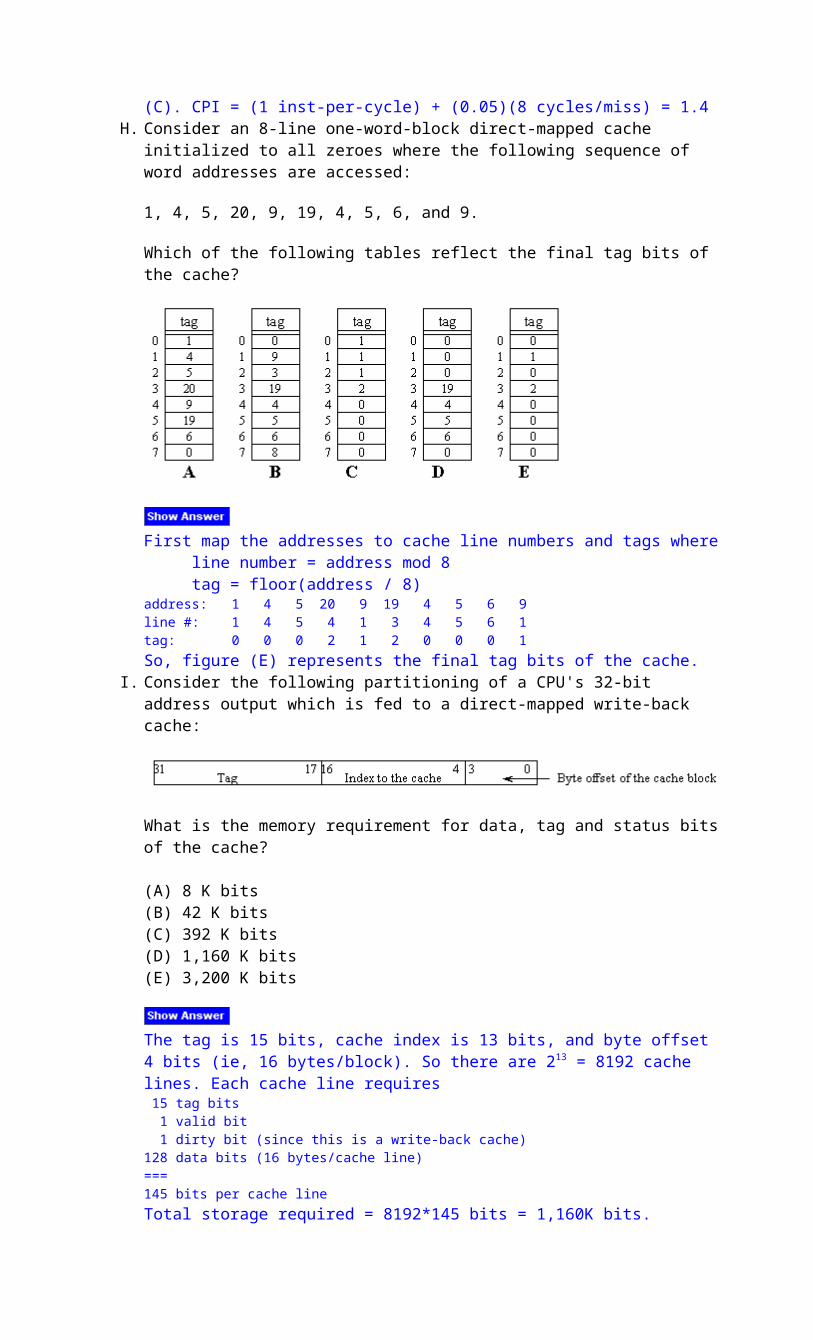
I. Consider the following partitioning of a CPU's 32-bit address output which is fed to a direct-mapped write-back cache:
What is the memory requirement for data, tag and status bits of the cache?
(A) 8 K bits(B) 42 K bits(C) 392 K bits(D) 1,160 K bits(E) 3,200 K bits
The tag is 15 bits, cache index is 13 bits, and byte offset 4 bits (ie, 16 bytes/block). So there are 213 = 8192 cache lines. Each cache line requires 15 tag bits 1 valid bit 1 dirty bit (since this is a write-back cache)128 data bits (16 bytes/cache line)===145 bits per cache line
Total storage required = 8192*145 bits = 1,160K bits.
Problem 3. A student has miswired the address lines going to the memory of an unpipelined BETA. The wires in question carry a 30-bit word address to the memory subsystem, and the hapless student has in fact reversed the order of all 30 address bits. Much to his surprise, the machine continues to work perfectly.
A. Explain why the miswiring doesn't affect the operation of the machine.
Since the Beta reverses the order of the 30 bit address in the same manner for each memory access, the Beta will use the same reversed address to access a particular memory location for both stores and loads. Thus, the operation of the machine will not be affected.
B. The student now replaces the memory in his miswired BETA with a supposedly higher performance unit that contains both a fast direct mapped cache and the same memory as before. The reversed wiring still exists between the BETA and this new unit. To his surprise, the new unit does not significantly improve the performance of his machine. In desperation, the student then fixes the reversal of his address lines and the machine's performance improves tremendously. Explain why this happens.
Caches take advantage of spatial locality by reading in an entire block of related data at one time, thereby reducing main memory accesses. By reversing the order of the 30 bit address, spatial locality of the memory is disrupted. The low-order bits that would normally place related data close to one another are instead the high-order bits and related data is more spread out through the main memory. This reduction in spatial locality reduces cache performance significantly. When the student fixes the address line reversal problem, spatial locality of the memory is restored, and the cache can perform as intended.
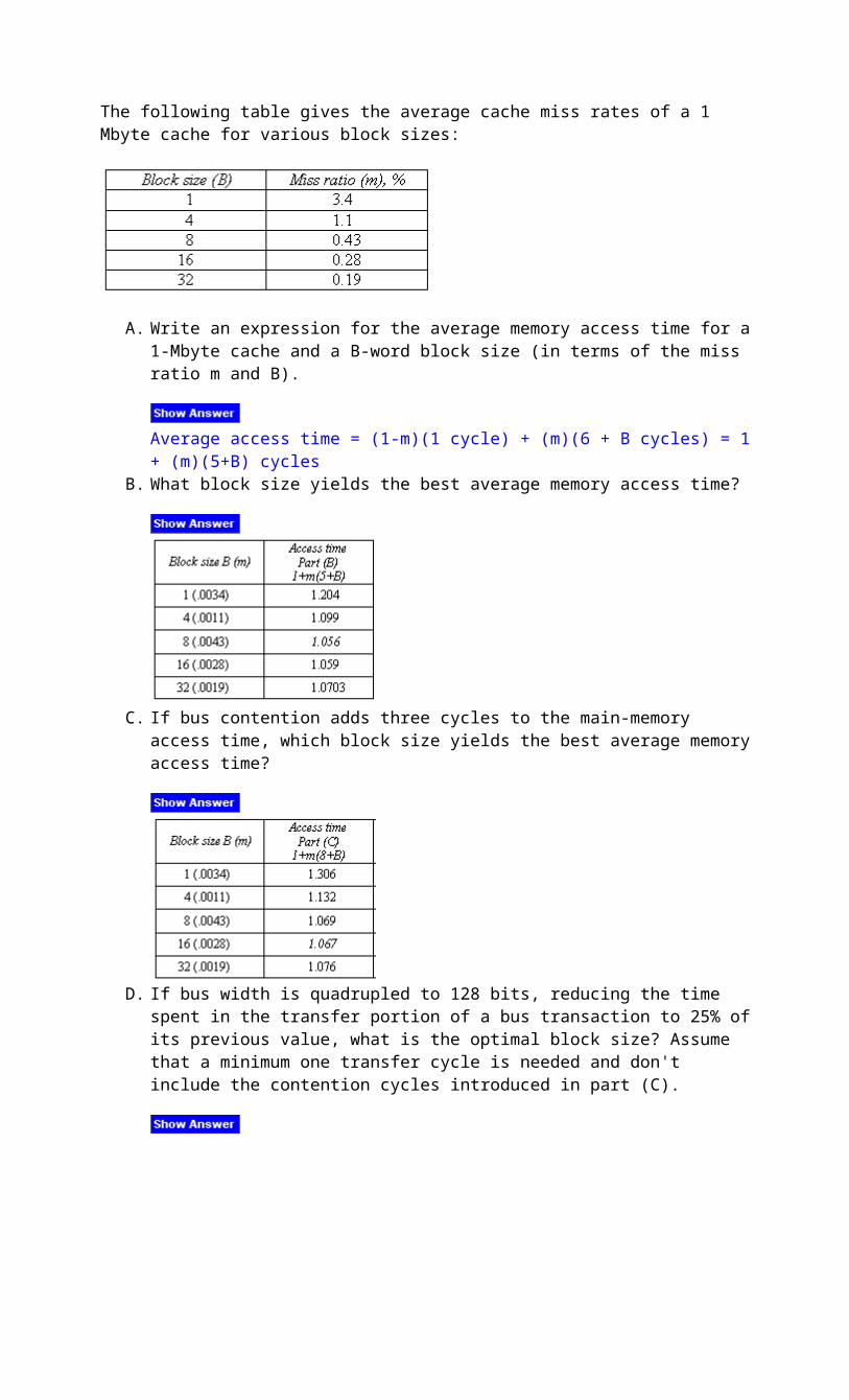
Problem 4. For this problem, assume that you have a processor with a cache connected to main memory via a bus. A successful cache access by the processor (a hit) takes 1 cycle. After an unsuccessful cache access (a miss), an entire cache block must be fetched from main memory over the bus. The fetch is not initiated until the cycle following the miss. A bus transaction consists of one cycle to send the address to memory, four cycles of idle time for main-memory access, and then one cycle to transfer each word in the block from main memory to the cache. Assume that the processor continues execution only after the last word of the block has arrived.
In other words, if the block size is B words (at 32 bits/word), a cache miss will cost 1 + 1 + 4 + B cycles. The following table gives the average cache miss rates of a 1 Mbyte cache for various block sizes:
A. Write an expression for the average memory access time for a 1-Mbyte cache and a B-word block size (in terms of the miss ratio m and B).
Average access time = (1-m)(1 cycle) + (m)(6 + B cycles) = 1 + (m)(5+B) cycles B. What block size yields the best average memory access time?
C. If bus contention adds three cycles to the main-memory access time, which block size yields the best average memory access time?
D. If bus width is quadrupled to 128 bits, reducing the time spent in the transfer portion of a bus transaction to 25% of its previous value, what is the optimal block size? Assume that a minimum one transfer cycle is needed and don't include the contention cycles introduced in part (C).
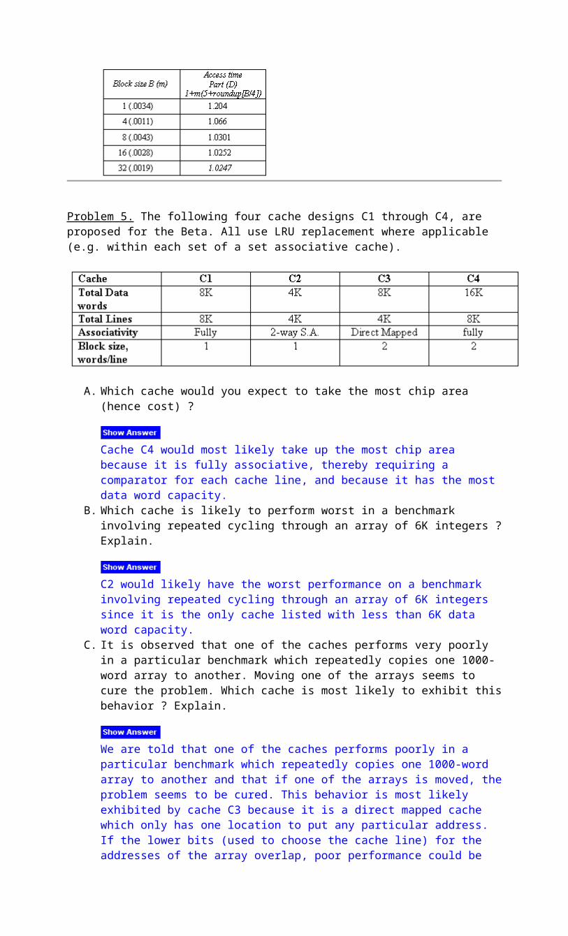
Problem 5. The following four cache designs C1 through C4, are proposed for the Beta. All use LRU replacement where applicable (e.g. within each set of a set associative cache).
A. Which cache would you expect to take the most chip area (hence cost) ?
Cache C4 would most likely take up the most chip area because it is fully associative, thereby requiring a comparator for each cache line, and because it has the most data word capacity.
B. Which cache is likely to perform worst in a benchmark involving repeated cycling through an array of 6K integers ? Explain.
C2 would likely have the worst performance on a benchmark involving repeated cycling through an array of 6K integers since it is the only cache listed with less than 6K data word capacity.
C. It is observed that one of the caches performs very poorly in a particular benchmark which repeatedly copies one 1000-word array to another. Moving one of the arrays seems to cure the problem. Which cache is most likely to exhibit this behavior ? Explain.
We are told that one of the caches performs poorly in a particular benchmark which repeatedly copies one 1000-word array to another and that if one of the arrays is moved, the problem seems to be cured. This behavior is most likely exhibited by cache C3 because it is a direct mapped cache which only has one location to put any particular address. If the lower bits (used to choose the cache line) for the addresses of the array overlap, poor performance could be observed. Moving the array so that the lower bits of the array addresses don't overlap could solve this problem.
D. Recall that we say cache A dominates cache B if for every input pattern, A caches every location cached by B. Identify every pair (A, B) of caches from the above list where A dominates B. Explain your reasoning.
So long as we are not using a random replacement strategy, it is always possible to come up with a benchmark that will make a particular type of cache have a miss on every data access. Thus, we cannot say that one particular type of cache always dominates another type of cache. However, we can compare two caches of the same type. Both C4 and C1 are fully associative caches with the same replacement strategy. We can say that C4 dominates C1 since C4 has a greater data word capacity.
Problem 6. The data-sheet for a particular byte-addressable 32-bit microprocessor reads as follows:
The CPU produces a 32-bit virtual address for both data and instruction fetches. There are two caches: one is used when fetching instructions; the other is used for data accesses. Both caches are virtually addressed. The instruction cache is two-way set-associative with a total of 212 bytes of data storage, with 32-byte blocks. The data cache is two-way set-associative with a total of 213 bytes of data storage, with 32-byte blocks
A. How many bits long is the tag field in each line of the instruction cache?
There are 32 = 25 bytes per block. The cache has 212 total bytes and is 2-way set associative, so each set has 211 bytes and thus 211/25 = 26 cache lines. So the address is partitioned by the cache as follows:
[4:0] = 5 address bits for selecting byte/word within a block[10:5] = 6 address bits for selecting the cache line[31:11] = 21 address bit of tag field
B. How many address bits are used to choose which line is accessed in the data cache?
There are 32 = 25 bytes per block. The cache has 213 total bytes and is 2-way set associative, so each set has 212 bytes and thus 212/25 = 27 cache lines. So the address is partitioned by the cache as follows:
[4:0] = 5 address bits for selecting byte/word within a block[11:5] = 7 address bits for selecting the cache line[31:12] = 20 address bit of tag field
C. Which of the following instruction addresses would never collide in the instruction cache with an instruction stored at location 0x0ACE6004?
(A) 0x0BAD6004 (D) 0x0ACE6838(B) 0x0C81C81C (E) 0xFACE6004(C) 0x00000004 (F) 0x0CEDE008
Collisions happen when instruction addresses map to the same cache line. Referring to the answer for (A), address bits [10:5] are used to determine the cache line, so location 0x0ACE6004 is mapped to cache line 0.
Only (D) 0x0ACE6838 maps to a different cache line and hence could never collide in the instruction cache with location 0x0ACE6004.
D. What is the number of instructions in the largest instruction loop that could be executed with a 100% instruction cache hit rate during all but the first time through the loop?
The instruction cache hold 212 bytes or 210 = 1024 instructions. So if the loop had 1024 instructions it would just fit into the cache.
Problem 7. The following questions ask you to evaluate alternative cache designs using patterns of memory references taken from running programs. Each of the caches under consideration has a total capacity of 8 (4-byte) words, with one word stored in each cache line. The cache designs under consideration are:
DM: a direct-mapped cache.
S2: a 2-way set-associative cache with a least-recently-used replacement policy.
FA: a fully-associative cache with a least-recently-used replacement policy.
The questions below present a sequence of addresses for memory reads. You should assume the sequences repeat from the start whenever you see "...". Keep in mind that byte addressing is used; addresses of consecutive words in memory differ by 4. Each question asks which cache(s) give the best hit rate for the sequence. Answer by considering the steady-state hit rate, i.e., the percentage of memory references that hit in the cache after the sequence has been repeated many times.
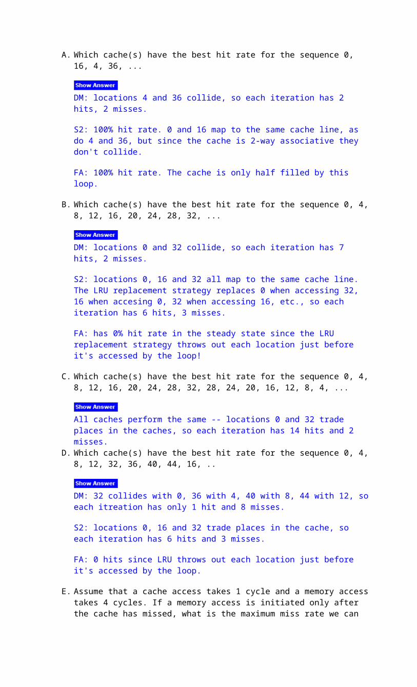
A. Which cache(s) have the best hit rate for the sequence 0, 16, 4, 36, ...
DM: locations 4 and 36 collide, so each iteration has 2 hits, 2 misses.
S2: 100% hit rate. 0 and 16 map to the same cache line, as do 4 and 36, but since the cache is 2-way associative they don't collide.
FA: 100% hit rate. The cache is only half filled by this loop.
B. Which cache(s) have the best hit rate for the sequence 0, 4, 8, 12, 16, 20, 24, 28, 32, ...
DM: locations 0 and 32 collide, so each iteration has 7 hits, 2 misses.
S2: locations 0, 16 and 32 all map to the same cache line. The LRU replacement strategy replaces 0 when accessing 32, 16 when accesing 0, 32 when accessing 16, etc., so each iteration has 6 hits, 3 misses.
FA: has 0% hit rate in the steady state since the LRU replacement strategy throws out each location just before it's accessed by the loop!
C. Which cache(s) have the best hit rate for the sequence 0, 4, 8, 12, 16, 20, 24, 28, 32, 28, 24, 20, 16, 12, 8, 4, ...
All caches perform the same -- locations 0 and 32 trade places in the caches, so each iteration has 14 hits and 2 misses.
D. Which cache(s) have the best hit rate for the sequence 0, 4, 8, 12, 32, 36, 40, 44, 16, ..
DM: 32 collides with 0, 36 with 4, 40 with 8, 44 with 12, so each itreation has only 1 hit and 8 misses.
S2: locations 0, 16 and 32 trade places in the cache, so each iteration has 6 hits and 3 misses.
FA: 0 hits since LRU throws out each location just before it's accessed by the loop.
E. Assume that a cache access takes 1 cycle and a memory access takes 4 cycles. If a memory access is initiated only after the cache has missed, what is the maximum miss rate we can tolerate before use of the cache actually slows down accesses?
If accesses always go to memory, it takes 4 cycles per access. Using the cache the average number of cycles per access is
1 + (miss rate)*4 So if the miss rate is larger than 75% the average number of cycles per access is more than 4.
Problem 8. Ben Bitdiddle has been exploring various cache designs for use with the Beta processor. He is considering only caches with one word (4 bytes) per line. He is interested in the following cache designs:
C1: 2-way set associative, LRU replacement, 256 total data words (128 sets of 2 words each).
C2: 2-way set associative, random replacement, 256 total data words (128 sets of 2 words each).
C3: 2-way set associative, LRU replacement, 512 total data words (256 sets of 2 words each).
C4: 4-way set associative, LRU replacement, 512 total data words (128 sets of 4 words each).
C5: Fully associative, LRU replacement, 512 total data words.
In order to help her analysis, Ben is trying to identify cases where one cache dominates another in terms of cache hits. Ben considers that cache A dominates cache B if, given identical strings
of memory references, every memory reference that gives a cache hit using B is also a hit using A. Thus if A dominates B, A will give at least as high a hit rate as B for every program.
In each of the following pairs of caches, deduce whether the first dominates the second:
A. C1 dominates C2
False. C1 has a 0% hit rate for 0, 256, 512, 0, 256, 512, ..., but C2 might do slightly better because it chooses the replacement set at random.
B. C2 dominates C1
No. C1 has a 100% hit rate for 0, 256, 0, 256, ..., but C2 might have an occasional miss. C. C3 dominates C1
Yes. C3 differs only in having a higher capacity than C1. D. C3 dominates C2
No. As we saw in (A) there are programs where LRU gets 0% hit rate and random may do slightly better, independently of the sizes of the caches.
E. C4 dominates C3
No. C4 has 0% hit rate on 0, 128, 256, 384, 512, 0, ... since all accesses map to the same cache line and LRU throws out the location just about to be accessed. In C3, 128 and 384 map to a different cache line than 0, 256 and 512, so manages a 40% hit rate in the steady state.
F. C4 dominates C2
No, for the same reason as (A) and (D). G. C5 dominates C1
No. Consider the following access pattern: 0, accesses to 512 uncached locations whose addresses don't map to cache line 0 for cache C1, 0, ...
C5 will replace location 0 on the 513th access and hence miss when 0 is accessed in the following cycle. C1 will have location 0 still in the cache when it's accessed again by the loop.
H. Averaged over a wide range of typical application programs, which of the above caches would you expect to yield the highest hit rate?
In general larger caches are better and fully associative caches are better than set associative caches, so C5 should have the highest hit rate.
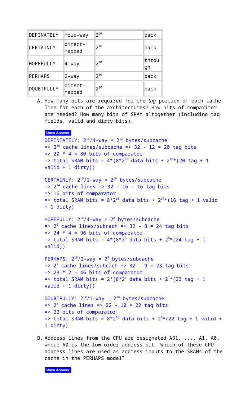
Problem 9. Adverbs Unlimited is considering a computer system based loosely on the Beta. Five designs have been proposed, each of them similar to the Beta except for a cache between the 32-bit processor data bus and the main-memory subsystem. Like the Beta, each machine deals with 32-bit main-memory addresses, for a total address space of 232 bytes. The machines' caches differ only in the parameters of associativity, size, and writeback. The block size for each cache 1 word (4 bytes).
Model Associativity Total data size (bytes) Write-
DEFINATELY four-way 216 back
CERTAINLY direct-mapped 216 back
HOPEFULLY 4-way 210 through
PERHAPS 2-way 210 back
DOUBTFULLY direct-mapped 210 back
A. How many bits are required for the tag portion of each cache line for each of the architectures? How bits of comparitor are needed? How many bits of SRAM altogether (including tag fields, valid and dirty bits).
DEFINIATELY: 216/4-way = 212 bytes/subcache=> 210 cache lines/subcache => 32 - 12 = 20 tag bits=> 20 * 4 = 80 bits of comparator=> total SRAM bits = 4*(8*212 data bits + 210*(20 tag + 1 valid + 1 dirty))
CERTAINLY: 216/1-way = 216 bytes/subcache=> 214 cache lines => 32 - 16 = 16 tag bits=> 16 bits of comparator=> total SRAM bits = 8*216 data bits + 214*(16 tag + 1 valid + 1 dirty)
HOPEFULLY: 210/4-way = 28 bytes/subcache=> 26 cache lines/subcach => 32 - 8 = 24 tag bits=> 24 * 4 = 96 bits of comparator=> total SRAM bits = 4*(8*28 data bits + 26*(24 tag + 1 valid))
PERHAPS: 210/2-way = 29 bytes/subcache=> 27 cache lines/subcach => 32 - 9 = 23 tag bits=> 23 * 2 = 46 bits of comparator=> total SRAM bits = 2*(8*29 data bits + 27*(23 tag + 1 valid + 1 dirty))
DOUBTFULLY: 210/1-way = 210 bytes/subcache=> 28 cache lines => 32 - 10 = 22 tag bits=> 22 bits of comparator=> total SRAM bits = 8*210 data bits + 28*(22 tag + 1 valid + 1 dirty)
B. Address lines from the CPU are designated A31, ..., A1, A0, where A0 is the low-order address bit. Which of these CPU address lines are used as address inputs to the SRAMs of the cache in the PERHAPS model?
PERHAPS is a 2-way set-associative cache with a total of 210 bytes, so each direct-mapped subcache contains 29 bytes. With a block size of 1 word (4 bytes), address bits [8:2] would be used as the index into the 32-bit-wide SRAM.
C. Suppose that address lines A2 and A9 were inadvertently interchanged in the cable between the DOUBTFULLY CPU and its cache. Which, if any, of the following statements best describes the effect(s) of this change, assuming that other hardware and software remain unmodified?
A. The machine would no longer work. B. The machine would continue to work as before. C. The machine would continue to work, but at a reduced performance level. D. The machine would continue to work, at an improved performance level.
(B). Address bits A2 through A9 are used as the cache index, interchanging them has no effect other than to change where in SRAM each cache line is stored, i.e., all the same locations are cached, they just happen to be stored in different cache SRAM locations than one might have expected.
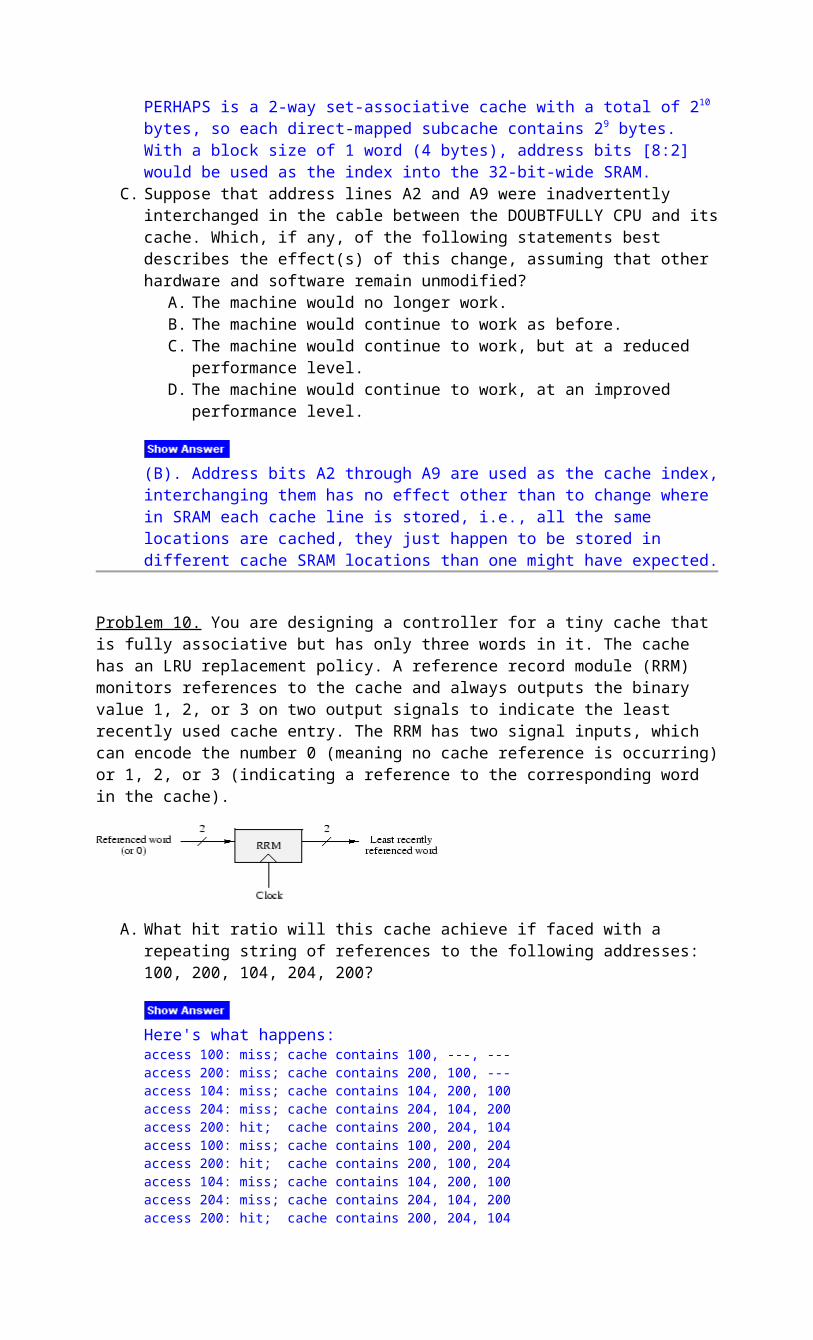
Problem 10. You are designing a controller for a tiny cache that is fully associative but has only three words in it. The cache has an LRU replacement policy. A reference record module (RRM)
monitors references to the cache and always outputs the binary value 1, 2, or 3 on two output signals to indicate the least recently used cache entry. The RRM has two signal inputs, which can encode the number 0 (meaning no cache reference is occurring) or 1, 2, or 3 (indicating a reference to the corresponding word in the cache).
A. What hit ratio will this cache achieve if faced with a repeating string of references to the following addresses: 100, 200, 104, 204, 200?
Here's what happens: access 100: miss; cache contains 100, ---, ---access 200: miss; cache contains 200, 100, ---access 104: miss; cache contains 104, 200, 100access 204: miss; cache contains 204, 104, 200access 200: hit; cache contains 200, 204, 104access 100: miss; cache contains 100, 200, 204access 200: hit; cache contains 200, 100, 204access 104: miss; cache contains 104, 200, 100access 204: miss; cache contains 204, 104, 200access 200: hit; cache contains 200, 204, 104...
So in the steady state, location 200 stays in the cache and all other locations get replaced. So the hit rate is 2/5 or 40%.
B. The RRM can be implemented as a finite-state machine. How many states does the RRM need to have? Why?
There are 3! = 6 ways to list the three locations in order of use. Thus RRM needs 6 states, one state for each possible order.
C. How many state bits does the RRM need to have?
We can encode six states using 3 state bits. D. Draw a state-transition diagram for the RRM.
E. Consider building an RRM for a 15-word fully associative cache. Write a mathematical expression for the number of bits in the ROM required in a ROM-and-register implementation of this RRM. (You need not calculate the numerical answer.)
There are 15! possible states, so we would need ceiling(log2(15!)) = 41 state bits. So the ROM would have 241 locations of 41 bits each, for a total of approximately 90 trillion bits.
F. Is it feasible to build the 15-word RRM above using a ROM and register in today's technology? Explain why or why not.
90 trillion bits is a bit much even for today's technology. In a .18u technology, a single transistor pulldown in a ROM might require (.2u x .5u) = .1u2, so our ROM would require about 9 square meters of silicon!
Gates and Boolean logic [Printable PDF version]
Problem 1. Gates and Boolean equations
A. Show the Boolean equation for the function F described by the following circuit:
_ _ _F(A,B,C,D) = A*B + A*C*D + A*B*C
B. Consider the circuit shown below. Each of the control inputs, C0 through C3, must be tied to a constant, either 0 or 1.
What are the values of C0 through C3 that would cause F to be the exclusive OR of A and B?
We want F to be 1 when A=1 and B=0, or when A=0 and B=1. So C0 = 0, C1 = 1, C2 = 1, C3 = 0.
C. Can any arbitrary Boolean function of A and B be realized through appropriate wiring of the control signals C0 through C3?
Yes. This circuit implements a 4-input MUX with its two select lines connected to A and B. By choosing the appropriate values for C0 through C3 we can implement any of the 16 possible Boolean functions of A and B.
D. Give a sum-of-products expression for each of the following circuits:
_ _(A) = A*B + B + C _ _
(B) = A*C + B*C _ _(C) = A*C + B*C _ _ _(D) = A*B + A*C*D + A*B*C _ _ _(E) = A*D + B*C + B*D
E. Give a canonical sum-of-products expression for the Boolean function described by each truth table below
We can construct a sum-of-products expression from a truth table by writing down a product term for each line of the table where the output is 1. Each product term contains all the input variables: directly (ie, "A") if that variable is 1 for this line of the truth table, or negated (ie, "not A") if that variable is 0 for this line of the truth table. We then OR the product terms together to get the final expression: _ _ _ _ _ _F(A,B,C) = A*B*C + A*B*C + A*B*C + A*B*C _ _ _G(A,B,C) = A*B*C + A*B*C + A*B*C + A*B*C
F. We've seen that there are a total of sixteen 2-input Boolean functions. How many 5-input Boolean functions are there?
There are 225 = 232 5-input boolean functions. To see why, recall that the truth table for a 5-input function will have 32 rows, one for each possible combination of the 5 inputs. The output column for each row can be filled in with one of two choices ("0" or "1"), for a total of 232 possible ways of filling in the output column for all 32 rows.
Problem 2. A priority encoder has inputs that are assigned some predetermined order. The output is the binary encoding of the first "1" valued input from the ordered list, and it is zero otherwise.
A. Give the truth table for a 3-input priority encoder.
Assume the inputs are A, B, C with A having priority 3, B priority 2 and C priority 1: A B C | P1 P0========|=========0 0 0 | 0 00 0 1 | 0 10 1 0 | 1 00 1 1 | 1 01 0 0 | 1 11 0 1 | 1 11 1 0 | 1 11 1 1 | 1 1
B. Give a sum of products realization of this priority encoder.
_ _ _ _ _ _ _P1 = A*B*C + A*B*C + A*B*C + A*B*C + A*B*C + A*B*C = A + B _ _ _ _ _ _ _P0 = A*B*C + A*B*C + A*B*C + A*B*C + A*B*C = A + B*C
Problem 3. Suppose we are building circuits using only the following three components:
inverter: tcd = 0.5ns, tpd = 1.0ns, tr = tf = 0.7ns 2-input NAND: tcd = 0.5ns, tpd = 2.0ns, tr = tf = 1.2ns 2-input NOR: tcd = 0.5ns, tpd = 2.0ns, tr = tf = 1.2ns
Consider the following circuit constructed from an inverter and four 2-input NOR gates:
A. What is tPD for this circuit?
tPD for the circuit is the maximum cumulative propagation delay considering all paths from any input to any output. In this circuit, the longest path involves three 2-input NAND gates with a cummulative tPD = 6ns.
B. What is tCD for this circuit?
tCD for the circuit is the minimum cumulative contamination delay considering all paths from any input to any output. In this circuit, the shortest path involves two 2-input NAND gates with a cumulative tCD = 1ns.
C. What is the output rise time for this circuit?
The output rise time is determined by tr of the gate connected to OUT. In this case, it's a 2-input NAND with tr = 1.2ns.
D. What is tPD of the fastest equivalent circuit (i.e., one that implements the same function) built using only the three components listed above?
The most straightforward way to determine the functionality of a circuit is to build a truth table: A B | OUT======|=====0 0 | 10 1 | 01 0 | 11 1 | 0
from which we can see that OUT = not B. We can implement this with a single inverter that has a tPD = 1ns.
Problem 4. Suppose that each component in the circuit below has a propagation delay (tpd) of 10ns, a contamination delay (tcd) of 1ns, and negligable rise and fall times. Suppose initially that all four inputs are 1 for a long time and then the input D changes to 0.
A. Draw a waveform plot showing how X, Y, Z, W and Q change with time after the input transition on D. First assume that the gates are not lenient. How will the waveforms change if the gates are lenient?
Waveforms with non-lenient gates:
Waveforms with lenient gates:
where we see that X doesn't change since the value of A is sufficient to determine the value of X.
Problem 5. The Mysterious Circuit X
A. Determine the function of the Circuit X, below, by writing out and examining its truth table. Give a minimal sum-of-products Boolean expression for each output.
B. For Circuit X assume that AND gates have a propagation of 2 nS and a contamination delay of 1nS, while XOR gates have a propagation delay of 3 nS and contamination delay of 2 nS.
Compute the aggregate contamination and propagation delays for Circuit X. What is the maximum frequency that the inputs of Circuit X be changed while insuring that all outputs are stable for 5 nS?
The contamination delay of the circuit is obtained from the shortest path form an input to an output. In circuit X this path start at A1 (or B1) and ends at P1, encountering only one AND gates. Thus tCD = 1ns.
The propagation delay of the circuit is obatined from the longest path from an input to an output. In circuit X this path starts at any of the inputs and ends at P4, encoutering two AND gates and one XOR gate. Thus tPD = 2ns + 2ns + 3ns = 7ns.
The answer to the next part is best understood by drawing a timing diagram:
Thus if the inputs transition no faster than every 11ns (~90 MHz), the outputs will be stable for at least 5ns.
C. Suppose the gates below are added to Circuit X. How are the answers to part b) affected?
The shortest path from input to output now passes through three AND gates for outputs P1 and P8 and one AND gate and an XOR gate for outputs P2 and P4. Thus
tCD = min(1ns + 1ns + 1ns, 1ns + 2ns) = 3ns.
The path that creats the largest propagation delay in the circuit is still the path from any input to P4, so tPD is still 7ns.
With this new circuit the inputs can transition every 9ns and still guarantee that the outputs will be stable for 5ns.
Problem 6. The Xilinx 4000 series field-programmable gate array (FPGA) can be programmed to emulate a circuit made up of many thousands of gates; for example, the XC4025E can emulate circuits with up to 25,000 gates. The heart of the FPGA architecture is a configurable logic block (CLB) which has a combinational logic subsection with the following circuit diagram:
There are two 4-input function generators and one 3-input function generator, each capable of implementing an arbitrary Boolean function of its inputs.
The function generators are actually small 16-by-1 and 8-by-1 memories that are used as lookup tables; when the Xilinx device is "programmed" these memories are filled with the appropriate values so that each generator produces the desired outputs. The multiplexer select signals (labeled "Mx" in the diagram) are also set by the programming process to configure the CLB. After programming, these Mx signals remain constant during CLB operation.
The following is a list of the possible configurations. For each configuration indicate how each the control signals should be programmed, which of the input lines (C1-C4, F1-F4, and G1-G4) are used, and what output lines (X, Y, or Z) the result(s) appear on.
A. An arbitrary function F of up to four input variables, plus another arbitrary function G of up to four unrelated input variables, plus a third arbitrary function H of up to three unrelated input variables.
Let X = F(F1, F2, F3, F4), Z = G(G1, G2, G3, G4), Y = H(C1, C2, C3). The necessary control signals are:
MA = 1MB = 1MC = 0 (select C1)MD = 1 (select C2)ME = 2 (select C3)
B. An arbitrary single function of five variables.
Let Y = F(A1, A2, A3, A4, A5). This can be implemented using both 4-input logic functions, and selecting between the two outputs with the 3-input logic function.
Z=f(A1, A2, A3, A4, 0), X=f(A1, A2, A3, A4, 1), Y= Z if A5=0, else Y=X
So Z is calculating F for the case when A5 = 0, X is calculating F for the case when A5 = 1, and Y is selecting between X and Z with a multiplexer function. A1-A4 represents F1-F4 and G1-G4 (they're connected to the same 4 inputs) and A5 represents C1. The necessary control signals are:
MA = 0MB = 0MC = X (value doesn't matter)MD = X (value doesn't matter)ME = 0 (select C1)
C. An arbitrary function of four variables together with some functions of six variables. Characterize the functions of six variables that can be implemented.
Let Z = G(G1, G2, G3, G4) - any function of 4 variables. X = F(F1, F2, F3, F4)Y = H(C1, C2, X) = H(C1, C2, G(F1, F2, F3, F4))
The functions of six variables which can be implemented (along with the 4-variable function) are all those functions that can be re-written as a function of 3 variables. The inputs to this function of three variables must be 2 of the original variables and some function of the remaining four variables. The necessary control signals are:
MA = 0MB = 1MC = X (value doesn't matter)MD = 0 (select C1)ME = 1 (select C2)
D. Some functions of up to nine variables. Characterize the functions of up to nine variables that can be implemented.
Let X = F(F1, F2, F3, F4)Z = G(G1, G2, G3, G4)Y = H(C1, X, Z) = H(C1, F(F1, F2, F3, F4), G(G1, G2, G3, G4))
The functions of nine variables that can be implemented are all those functions that can be re-written as a function of 3 variables. The inputs to this three-variable function will be one of the original variables, plus two separate functions of 4 variables (these two 4-variable functions will have the remaining 8 original variables as inputs).
MA = 0MB = 0MC = X (value doesn't matter)MD = X (value doesn't matter)ME = 0 (select C1)
E. [Optional challenge] Can every function of six inputs be implemented? If so, explain how. If not, give a 6-input function and explain why it can't be implemented in the CLB.
The functions of 6 variables which we can implement must be of the form Y = y(C1, C2, f(F1,F2,F3,F4))
or of the form
Y = y(C1, f(F1, F2, F3, F4), g(G1, G2, G3, G4))
(this second function will have some overlap between C1, F1-4, and G1-4; some variables will be connected to multiple inputs) Essentially, the functions we are able to implement are only those for which we can factor a set of 4 variables out of the equation. For example, the following function cannot be implemented by the CLB:
Y = A1A2A3A4A5 + A1A2A3A4A6 + A1A2A3A5A6 + A1A2A4A5A6 + A1A3A4A5A6 +A2A3A4A5A6
This function cannot be broken down into either of the forms mentioned above.
Disks and I/O
Q: list the three main delays in getting data from disk, in increasing average delays (or increasing importance, since the more delay, the more important it is)
A: transfer delay, rotational delay, seek delay.
Q: What does the acronym DMA stand for? Describe what is the advantage of a system that has a DMA over a system that has no DMA
A: Direct Memory Access: in a system with DMA, the CPU can run applications without being involved in the transfer of data from a device to main memory.
Q: if all subcomponents of system use the bus to get data from memory and the CPU needs data from memory to run the application, why does using a DMA allow for higher performance?
A: after a chunk of memory was read (say 4KB) into cache, the CPU will not read anything from memory until a cache miss was detected.
Q: Describe the organ-pipe distribution and mention why it is a good tool increase the performance of disks.
A: placing the most used blocks of data close together in order to reduce the seek time, which is the most important delay in disk performance. the organ-pipe distribution places data this way, using a histogram and allowing the most used blocks of data to be in the same track, the next most used blocks in the next tracks, etc.
Q: what is the sequence of software layers that are traversed from the time a user needs to read a disk block until the time the data is available to the user (from library call to the return from the library call). among the layers are:a) libraries, b) page replacement algorithms. c) ISRs, d) Device-independent OS software, e) data placement algorithms, f) de-framentation software, g) device drivers, h) controllers, i) device itself
A: libraries --> Device-independent OS software --> device drivers --> controller --> device --> ISR --> device drivers --> Device-independent OS software --> libraries.
A full-adder is represented by the following Boolean equation;
S = A B C
Cout = (A B)Cin + AB
Given that the following gate delays;
EXOR = 4nsAND = 3nsOR = 2ns
a) Determine the time delay required to obtain S(4) and C(5)
b) Derive the general expressions for obtaining the time delays for Si and Ci+1
In a virtual memory system, an 8KB page is swapped into main memory. This page is stores on a hard disk with the following parameters:
Average track diameter = 6cmSpeed of rotation = 10,800 RPMAverage seek time = 5msSeek time between consecutive tracks = 1msLinear density = 100,000 bits/cmController overhead = 2ms
a. How many sectors and tracks are required to store one page of data?
data per track = phi * 6 * 100,000 = 235500 bytes# tracks = 8KB/23500B = 0.035# sectors =
(b) ave seek time + ave rotational delay + transfer time + control overhead= 5ms + 0.5*60*1000/10800ms + 0.035*60*1000ms + 2ms = 10ms
(c) 500M cycles/sec * 10 ms = 5000000 cycles
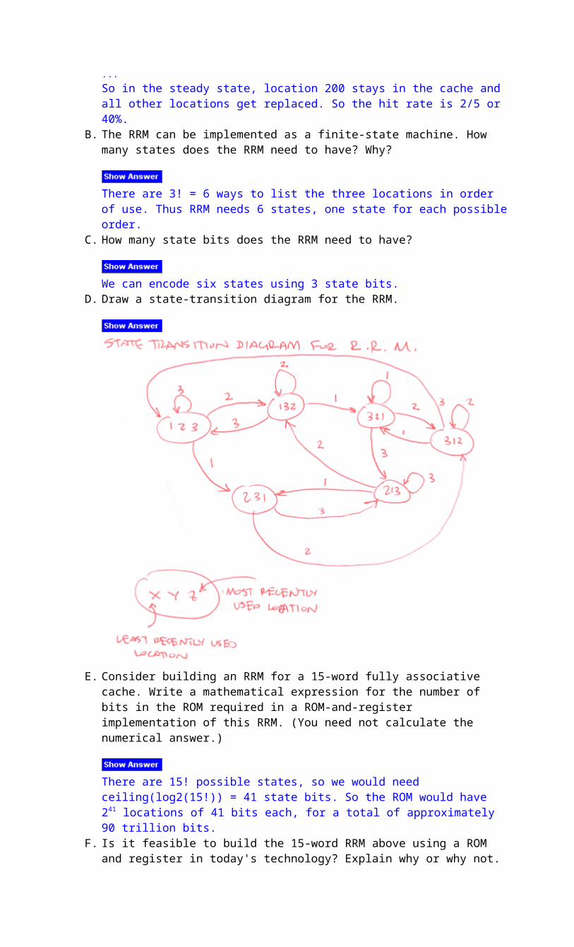
(d) 20M cycles/sec * 8KB/(40MB/sec) = 4000 cycles.
Name____________________________ WPI SID:___________
Computer ArchitectureCS4515 – C-TermProf. Colon Osorio
Exam # 1, January 23, 2004
SolutionsI. I. Multiple Choice (1 point each)
1. 1. Computer Architecture is: B
a. a. The art of designing buildings b. Intersection of Machine Organization and Instruction
` Set Design
a. c. The design of Microprocessors d. A Design Process 2. 2. Computer Architecture is a science that focuses on design tradeoffs across multiple levels of
abstraction.
True____X___ False_______
3. 3. Within the context of Computer Architecture, Semantic Gap is: D
a. a. A greek Word b. Difference between assembly language and
` Machine language
a. c. A measure of Distance between the d. A measure of Distance between the
Representation of a Problem at different Levels Representation of a Problem at different LevelsWithin a the execute unit. Of Abstraction, from a High Level
Language (like Java) to Transistors. 4. 4. Assembly Language is: C
a. a. A symbolic Language that can be b. Language used by the Intel, HP, and COMPAQ
Translated into PseudoIntructions
a. c. Language that a Computer Understands d. Pseudointsruction
5. 5. Computer Organization is: D
a. a. The description of Intel’s Pentium IV uprocessors b. Fetch, Decode, and Execute logic.
a. c. Register Transfer Level (RTL) d. Translation of ISA into Functional
Componentssuch as ALU, REG File, etc.
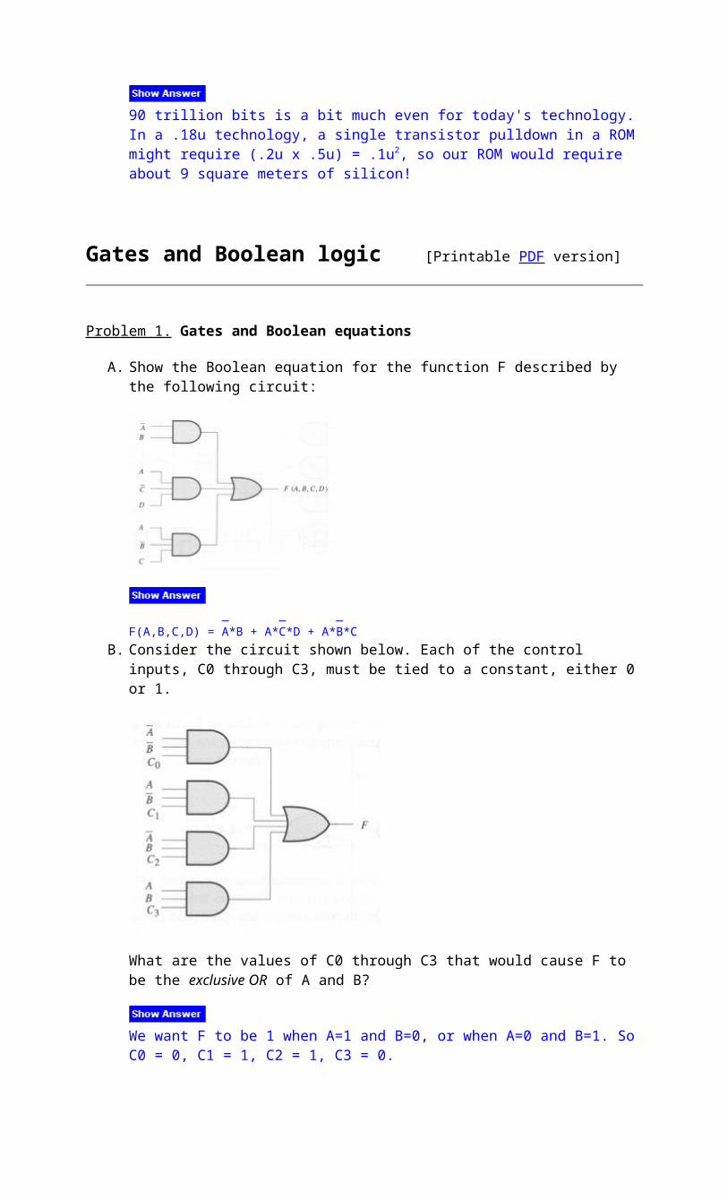
6. 6. A defect is:A
a. a. Microscopic flaw in a wafer b. Determines the performance of a wafer
a. c. ALU d. Measure of Yield
7. 7. ISA stands for:
a. a. The internal organization of a uprocessor b. A Logic Family just like TTL, CMOS, ECL
a. c. Instruction Set Algorithm d. Instruction Set Architecture
8. 8. Yield in the fabrication of Integrated circuits is: D
a. a. Proportional to (wafer diameter) 8 b. the cost of a single die
a. c. The # of defects on a single microprocessor d. % of good dies from total number of dies in a wafer
9. 9. Moore’s Law States that number of transistors per square inch on integrated circuits had doubled
every year since the integrated circuit was invented.
True_________ False____X___
10. 10. An example of an ISA is: C
a. a. 2.4 GHZ Pentium Computer b. Alpha 21164 microprocessor
a. c. Intel MMX d. IBM 360 Model 91
11. 11. Amdahl’s Law states that the speedup due to the enhancement, E, or feature added to an
existing design can be calculated as follows:
Speedup = Execution Time (without the enhancement) / Execution Time (with the enhancement)
True____X_____ False_______
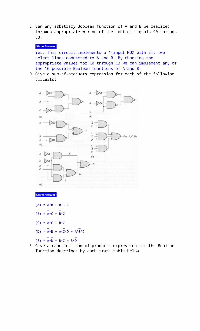
12.12. In general, the execution time of a program is given by the following formula: B
a. a. MIPS / # instructions in program b. # instructions X average # cycles per instruction X cycle time
a. c. Cycle time X clock rate d. # instructions in program / MFLOPS
13.13. In the battle of the microprocessors, that is, Intel vs. AMD. INTEL has a significant advantage because of their: D
a. a. Smaller Volumes (i.e., number of uprocessors sold) b. Smallest wafer size
a. c. ISA architecture Pentium vs. Athlon d. Semiconductor
Technology – 90 nanometers vs.130 nanometers for AMD
14. 14. In measuring performance, a popular metric surfaced in the 1970’s decade, called MFLOPS, also
known as mega flops. MegaFlops refers to the number (in millions) of floating point operations executed per second. The formula used to compute megaflops is:
MFLOPS = Number of floating-point operations in a program / Execution Time of Program (in seconds) X 106
True____X_____ False_______
15. 15. Compiler technology can affect the average cycles per instruction executed (average cpi). by:
a. a. Mapping Registers and Instructions in code b. minimizing cycle timeGenerated to avoid utilization conflicts.
a. c. Maximizing # instructions issued d. minimizing execution time
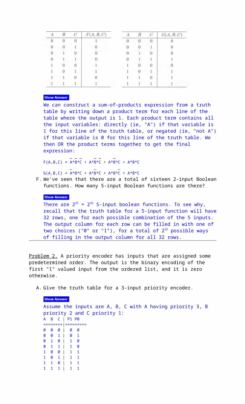
Problems (25 points each). 16.16. Amdahl's Law is a law governing the speedup of enhancement to a particular
architecture. Amdahl’s law has been used effectively in the design as an approximation for true speedup of the enhancement. Specifically, it has been use to compute the potential speedup using multiprocessor implementations. The law states that
Speedup = Execution Time (without Enhancement) / Execution Time (with Enhancement) Assume, that you are considering the design of a four- (4) processor system. Further assume, that only 16 % of the execution time of the code is parallelizable (that is, it can be executed in parallel by more than one processor). Compute the speedup using Amdahl’s law of the four- (4) processor implementation over the single processor implementation. Solution:
SPEEDUP = Exec old / Exec new
Exec new = Exec old [(1-fracwithout enhancemnet) + fracenhanced / speedup)]
SPEEDUP = 1 / [(1-FRAC) + FRAC /SPEEDUP]
= 1 / [.85 + 0 .16/4] = 1 / .89 = 1.123 17.17. Consider two different implementations, M1 and M2, of the same instruction set.
There are three classes of instructions (A, B, and C) in the instruction set. M1 has a clock rate of 1600 MHz, and M2 has a clock rate of 800 MHz. The average number of cycles per instruction (CPI) for each class of instruction on M1 and M2 is given in the following table:
ClassInstruction Class
CPI on M1
CPI on M2
Instruction mix for C1
Instruction mix for C2
Instruction mix for C3
A LW/SW 4 2 30% 30% 50%
B Arithmetic 6 4 50% 20% 30%
C Branches 8 3 20% 50% 20%
The table also contains a summary of how three different compilers use the instruction set. C1 is a compiler produced by the makers of M1, C2 is a compiler produced by the makers of M2, and C3 is compiler produced by an independent compiler vendor. Assume that each compiler generates the same number of instructions for a given program but that the instruction mix is as described in the table above.
a. a. If you use compiler C1 on M1 what is the average CPI of M1?
avg cpi = avg cpiith X fraction ith
= 0.3 (4 ) + 0.5 (6) + 0,2 (8) = 1.2 + 3.0 + 1.6 = 5.8
b. b. Using C2 on both M1 and M2, how much faster can the makers of M2 claim that M2 is compared with M1?
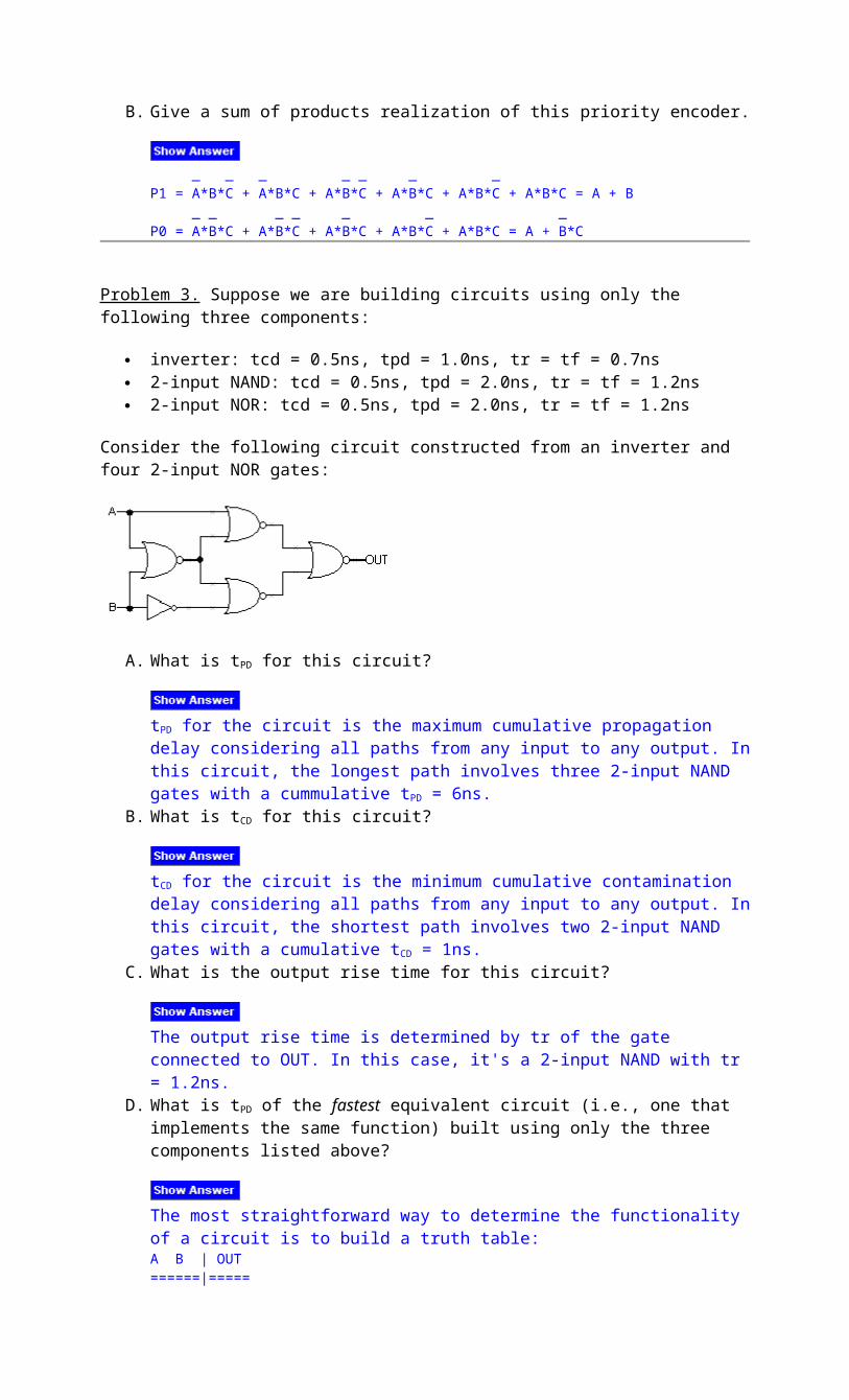
# instrs X avg cpi for M1 X cycle time for M1Speedup = _____________________________________________
# instrs X avg cpi for M2 X cycle time for M2
avg cpi for M1 X cycle time for M1Speedup = _____________________________________________
avg cpi for M2 X cycle time for M2 [ 0.3 (4) + 0.2 (6) + 0.5 ( 8) ] X 1/1600
= _____________________________________________[ 0.3 (2) + 0.2 (4) + 0.5 (3) ] X 1/800
= 6.4 / 5.8 = 1.103