Embed Size (px)
Citation preview

Company Presentation February 2011
Company Presentation
May 2011

1
Disclaimer
This presentation contains forward-looking statements relating to the
business, financial performance and earnings of SUSS MicroTec AG and
its subsidiaries and associates. Forward-looking statements are based on
current plans, estimates, projections and expectations and are therefore
subject to risks and uncertainties, most of which are difficult to estimate
and which in general are beyond the control of SUSS MicroTec AG.
Consequently, actual developments as well as actual earnings and
performance may differ materially from those which are explicitly or
implicitly assumed in the forward-looking statements. SUSS MicroTec AG
does not intend or accept any obligation to publish updates of these
forward-looking statements.

2
Content
I. Executive Summary
II. Products and Markets
III. Growth Opportunities
IV. Financials
V. Outlook
VI. Appendix

3
SUSS MicroTec Spotlight
Key Data*:
� Bloomberg Symbol: SMH
� TecDax
� Share price: 11,73 €
� Market Cap: 220 Mio. €
� Enterprise Value: 185 Mio. €
� SUSS MicroTec: A global leader in semiconductor equipment
� Our equipment and process solutions create the micro structures that build and
connect micro electronic devices
� We are focused on high growth market segments:
Semiconductors, MEMS, LEDs
* April 29, 2011
4
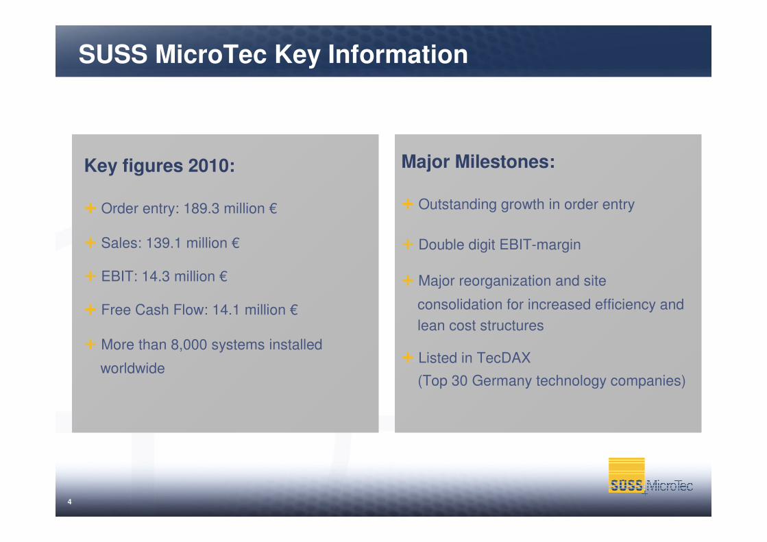
SUSS MicroTec Key Information
Key figures 2010:
� Order entry: 189.3 million €
� Sales: 139.1 million €
� EBIT: 14.3 million €
� Free Cash Flow: 14.1 million €
� More than 8,000 systems installed
worldwide
Major Milestones:
� Outstanding growth in order entry
� Double digit EBIT-margin
� Major reorganization and site
consolidation for increased efficiency and
lean cost structures
� Listed in TecDAX
(Top 30 Germany technology companies)

5
12 Months Business Development
Order Entry in € million
Sales in € million
50.6
56.9
49.548.3
32.0
42.537.037.7
Q2/2010 Q3/2010 Q4/2010 Q1/2011
Order Entry over thelast 12 Months: ~ 205 € million
Sales over the last12 Months: ~ 150 € million

6
Stock Performance 2011
(Price of the SUSS MicroTec Share at December 30, 2010: € 9.14)
4 months average daily trading volume: 310,000
50
100
150
Jan. Feb. M rz. Apr. M ai.
SÜ SS M icroTec, indexed TecD A X , indexed Prime IG Semiconduct or, indexed
7
Content
I. Executive Summary
II. Products and Markets
III. Growth Opportunities
IV. Financials
V. Outlook
VI. Appendix

8
SUSS MicroTec In The Value Chain
Research Institutes
ICs & Components End Products End UserEquipment
Supplier
9
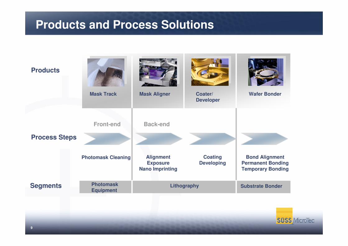
Products and Process Solutions
Mask Aligner Coater/ Developer
Wafer Bonder
Products
CoatingDeveloping
Alignment Exposure
Nano Imprinting
Bond AlignmentPermanent BondingTemporary Bonding
Process Steps
Mask Track
Photomask Cleaning
Front-end Back-end
PhotomaskEquipment
Segments Lithography Substrate Bonder

10
Mega Trends Driving our Key Markets
MEMS
LED
Key Markets
Sensors
Electronics
Solid State Lighting
SemiconductorsFront End
Back End
Energy Efficiency
Computing
Communication
Entertainment
Transportation

11
Enabling Semiconductor Trends
� SUSS MicroTec drives and enables the fundamental challenges of the semiconductor Industry:
� The SUSS MicroTec family of products provides equipment and process solutions for 2-dimensional and 3-dimensional scaling

12
Semiconductors
� SUSS MicroTec offers solutions for performance and yield critical steps in semiconductor manufacturing
� Front End: Mask Cleaning
� Back End: Advanced Packaging
3D Integration
Stacking chips allows for higher device complexity
Micro-bumping replaces wire-bonding for high-end integrated circuits
10 mm
30 mm
Advanced PackagingAdvanced Packaging 3D Integration3D Integration
Mask CleaningMask Cleaning
Maintains mask integrity of 193i sub 22nm, EUVL and NIL lithography

13
MEMS and LED
� Ultra High Brightness Light Emitting Diodes ( UHB LED) for solid state lighting
� UHB LEDs drive rapidly growing LED markets like automotive, consumer electronics and lighting applications
MEMSMEMS LEDLED
� Micromechanical devices with electrical functions
� Micro Electro Mechanical Systems are found in a wide application range from automotive over industrial process control sensors to consumer products
� For MEMS and LED production SUSS MicroTec offers a comprehensive suite of products: Mask Aligners – Coaters / Developers – Wafer Bonders

14
From Advanced Packaging to 3D Integration
� Technical and economical limitations increasingly slow down the shrink roadmap of integrated circuits
� Going into the third dimension by stacking chips allows for a further complexity increase of integrated devices
� 3D integration promises greater space efficiency, lower power consumption and a significant increase in performance.
� SUSS MicroTec develops equipment and processes for 3D Integration

15
3D Integration: Chip Design Using the Third Dimension
Source: Yole Développement (2010)

16
Content
I. Executive Summary
II. Products and Markets
III. Growth Opportunities
IV. Financials
V. Outlook
VI. Appendix

17
Growth Opportunities
� The company’s long term growth perspective derives from the double digit growth rates of the target markets 3D Integration, Advanced Packaging, LED and MEMS
� SUSS MicroTec is one of the leading suppliers for wafer bonders in the semiconductor industry offering a broad portfolio of permanent and temporary bonding equipment and process solutions
Source: Yole Développement
� The wafer bonder equipment market is estimated to grow rapidly to a size of larger 500 million $ within the next few years
� SUSS MicroTec targets a market
share of 30%+ which is in line with
the current market position
18
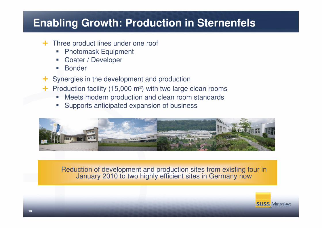
Enabling Growth: Production in Sternenfels
� Three product lines under one roof � Photomask Equipment� Coater / Developer � Bonder
� Synergies in the development and production
� Production facility (15,000 m²) with two large clean rooms
� Meets modern production and clean room standards� Supports anticipated expansion of business
Reduction of development and production sites from existing four in January 2010 to two highly efficient sites in Germany now
19
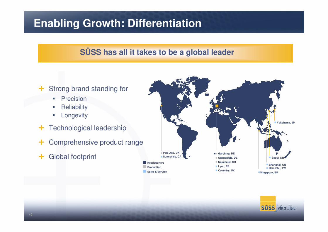
Enabling Growth: Differentiation
SÜSS has all it takes to be a global leader
� Strong brand standing for
� Precision
� Reliability
� Longevity
� Technological leadership
� Comprehensive product range
� Global footprint
Production
Headquarters
Sales & Service
Palo Alto, CA
Shanghai, CNHsin Chu, TW
Singapore, SG
Garching, DE
Sternenfels, DE
Neuchâtel, CH
Lyon, FR
Coventry, UK
Yokohama, JP
Seoul, KRSunnyvale, CA

20
Content
I. Executive Summary
II. Products and Markets
III. Growth Opportunities
IV. Financials
V. Outlook
VI. Appendix

21
Key Financials continuing operations
in € million Q1 2011 Q1 2010 FY 2010 FY 2009
Order Intake 48.3 32.3 189.3 93.3
Order Backlog (end of period) 130.5 75.4 116.1 57.0
Revenue 32.0 21.9 139.1 103.9
EBIT 2.5 -0.1 14.3 2.8
EBIT in % of Sales 7.8% -0.2% 10.3% 2.7%
Earnings after tax 2.4 -0.7 13.0 0.5
EPS in € (basic) 0.13 -0.04 0.71 0.03
Employees 647 579 616 498
Free Cash Flow* -2.2 -1.3 14.1 8.9
Net Cash** 35.1 11.0 34.6 18.4
* Before consideration of purchase or sale of available-for-sale securities and before consideration of extraordinary items from purchase or sale of subsidiaries
** incl. interest-bearing securities

22
Content
I. Executive Summary
II. Products and Markets
III. Growth Opportunities
IV. Financials
V. Outlook
VI. Appendix
23
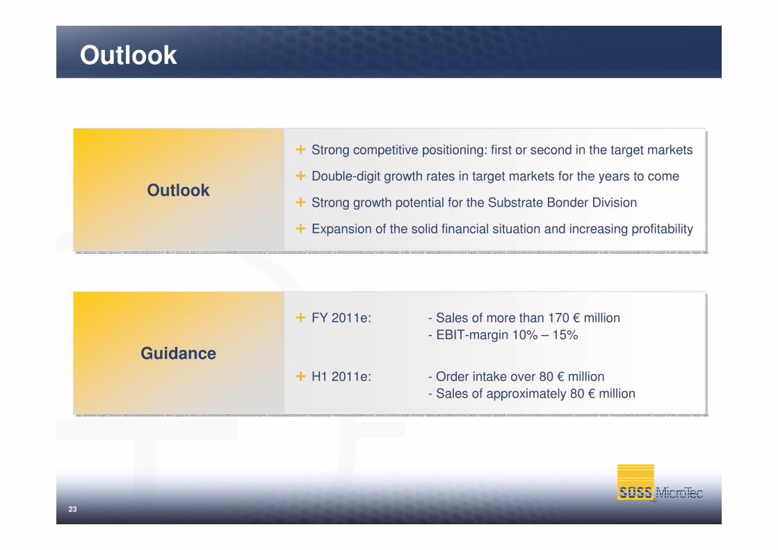
Outlook
OutlookOutlook
� Strong competitive positioning: first or second in the target markets
� Double-digit growth rates in target markets for the years to come
� Strong growth potential for the Substrate Bonder Division
� Expansion of the solid financial situation and increasing profitability
GuidanceGuidance
� FY 2011e: - Sales of more than 170 € million
- EBIT-margin 10% – 15%
� H1 2011e: - Order intake over 80 € million
- Sales of approximately 80 € million

24
Investment case
� Strong balance sheet
� Lean cost structure
� Strong fundamental growth in target markets
� Significant mid term revenue opportunity
� Strong competitive positioning: first or second in the target markets
� Evolve from Lithography company to leading company in the
semiconductor backend, enabling 3D integration
� Participate in the consolidation of the backend
25
Content
I. Executive Summary
II. Products and Markets
III. Growth Opportunities
IV. Financials
V. Outlook
VI. Appendix

26
Long Term Development of the SUSS Share
(Price of the SUSS MicroTec Share at January 4, 2010: € 4,40)
Average daily trading volume: ~170,000
0
50
100
150
200
250
300
Jan. Feb. M rz. Apr. M ai. Jun. Jul. Aug. Sep. Okt. Nov. Dez. Jan. Feb. M rz. Apr. M ai.
SÜ SS M icroT ec, indexed TecD A X , ind exed Prime IG Semiconduct or , indexed

27
Ownership Information
310,000 SharesØ Trading Volume per day in 2011
SemiconductorsSegment
Equinet Bank AG Close Brothers Seydler Bank AGDesignated Sponsor
Xetra, Frankfurt, Hamburg,Berlin – Bremen, Dusseldorf,
Stuttgart, MunichTradable at
Frankfurt, Regulatory MarketListing
Prime StandardStock Market Segment
Ownership information (04/30/11)
No-par value sharesStock Category
18,721,038Number of registered Shares
DE0007226706ISIN
722670WKN
SMHG
SMH
ca. € 220 million
Reuters Symbol
Bloomberg Symbol
Market Capitalization (04/30/2011)
Free Float 87.97 %
Credit Suisse 3.35 %
DWS 8.68 %

28
Investor Relations Information
Tel.: +49 (0) 89-32007- 161Fax.: +49 (0) 89-32007- 451Email: [email protected]
SÜSS MicroTec AGSchleissheimer Strasse 9085748 Garching (Munich)Germanywww.suss.com
Franka Schielke
Contact Financial Calendar 2011
Photonics Conference, Munich May 24
DZ Bank Sustainable Technologies Conference, Zurich June 8
UniCredit European Forum, San Francisco June 8 / 9
Close Brothers Seydler Conference, Paris June 27 / 28
Interim Report 2011 August 4
UBS Best of Germany Conference, New York September 14 / 15
Nine-month Report 2011 November 8
TMT Conference Morgan Stanley, Barcelona November 16 - 18
German Equity Forum Fall 2011 Novemer 21 - 23

29
Segment Reporting 2010 continuing operations
in € million
LithographySubstrate
BonderPhotomask Equipment
Others Total
Order Intake
2010 118.9 23.6 39.0 7.8 189.3
2009 73.0 18.8 -- 4.5 96.3
Revenue
2010 88.9 24.7 18.4 7.0 139.1
2009 77.6 18.3 -- 8.0 103.9
Segment-EBIT
2010 17.0 -7.1 2.1 2.3 14.3
2009 11.7 -3.8 -- -5.1 2.8
Segment-EBIT-margin
2010 19.1 % -28.7 % 11.4 % 32.9 % 10.3 %
2009 15.1 % -20.8 % -- -63.8 % 2.7 %
Employees as of 12/31
2010 324 141 91 60 616
2009 325 119 -- 54 498

30
63 %
12 %
4 %21 % Photomask
Cleaning
Lithography
Substrate Bonder
Others
Order Entry Analysis 2010 continuing operations
48 %
8 %
18 %
26 %
Europe
North America
Japan
Rest of Asia
by Segment
by Regions
----39.0Photomask Cleaning
+ 97 %96.3189.4Total
+ 74 %4.57.8Others
+ 25 %18.823.6Substrate Bonder
+ 63 %73.0118.9Lithography
%20092010In € million
+ 60% 56.990.9Rest of Asia
+ 97 %96.3189.4Total
+ 216 %4.614.5Japan
+ 129 %21.850.0Europe
+ 161 %13.033.9North America
%20092010in € million

31
55 %
5 %
14 %
26 %
Europe
North America
Japan
Rest of Asia
64 %
18 %
5 %13 % Photomask
Cleaning
Lithography
Substrate Bonder
Others
Sales Analysis 2010 continuing operations
by Segment
by Regions
----18.4Photomask Cleaning
103.9
8.0
18.3
77.6
2009
+ 34 %139.1Total
- 12 %7.0Others
+ 35 %24.7Substrate Bonder
+ 15 %88.9Lithography
%2010in € million
103.9
42.2
10.5
30.1
21.1
2009
+ 81 %76.5Rest of Asia
+ 34 %139.1Total
- 34 %6.9Japan
+ 22 %36.7Europe
- 10 %19.0North America
%2010in € million
32
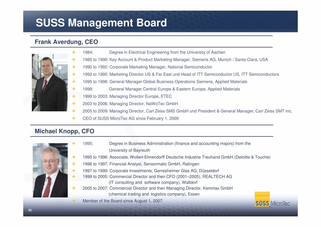
SUSS Management Board
Frank Averdung, CEO
Michael Knopp, CFO
� 1995: Degree in Business Administration (finance and accounting majors) from the
University of Bayreuth
� 1995 to 1996: Associate, Wollert-Elmendorff Deutsche Industrie Treuhand GmbH (Deloitte & Touche)
� 1996 to 1997: Financial Analyst, Sensormatic GmbH, Ratingen
� 1997 to 1999: Corporate Investments, Gerresheimer Glas AG, Düsseldorf
� 1999 to 2005: Commercial Director and then CFO (2001–2005), REALTECH AG
(IT consulting and software company), Walldorf
� 2005 to 2007: Commercial Director and then Managing Director, Kemmax GmbH
(chemical trading and logistics company), Essen
� Member of the Board since August 1, 2007
� 1984: Degree in Electrical Engineering from the University of Aachen
� 1985 to 1990: Key Account & Product Marketing Manager, Siemens AG, Munich / Santa Clara, USA
� 1990 to 1992: Corporate Marketing Manager, National Semiconductor
� 1992 to 1995: Marketing Director US & Far East und Head of ITT Semiconductor US, ITT Semiconductors
� 1995 to 1998: General Manager Global Business Operations Siemens, Applied Materials
� 1998: General Manager Central Europe & Eastern Europe, Applied Materials
� 1999 to 2003: Managing Director Europe, ETEC
� 2003 to 2006: Managing Director, NaWoTec GmbH
� 2005 to 2009: Managing Director, Carl Zeiss SMS GmbH und President & General Manager, Carl Zeiss SMT Inc.
� CEO of SUSS MicroTec AG since February 1, 2009

33
Strategic Restructuring Measures
Consolidation of Production Sites
Readjustments of Product Lines
Resizing of Field Offices to Meet Current and Future Business Requirements
• From four at the beginning of 2010 to two by Q1, 2011
• Moved three product lines under one roof in Sternenfels
• Established Sternenfels as the main SUSS production site
• Closed Bangkok office
• Reduced size of the Japan office
• Increased Taiwan and China organizations
• Consolidated „Rest of Asia“ in Singapore
• Opened office in DongTan, Korea
• Moved US sales and service organization to Silicon Valley
• Sold loss making Test Systems division
• Acquired HamaTech APE
• Relocated the Substrate Bonder Division from the US to Germany
3434
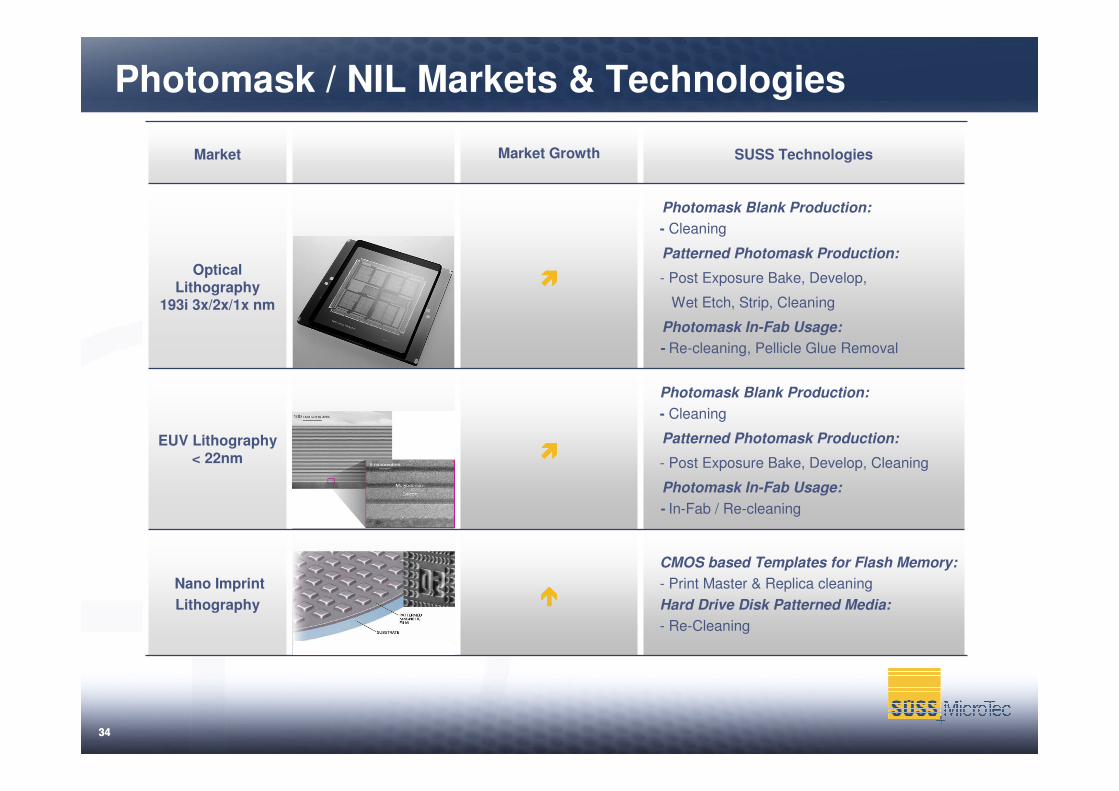
Photomask / NIL Markets & Technologies
Market Market Growth SUSS Technologies
OpticalLithography
193i 3x/2x/1x nm
����
Photomask Blank Production:
- Cleaning
Patterned Photomask Production:
- Post Exposure Bake, Develop,
Wet Etch, Strip, Cleaning
Photomask In-Fab Usage:
- Re-cleaning, Pellicle Glue Removal
EUV Lithography< 22nm ����
Photomask Blank Production:
- Cleaning
Patterned Photomask Production:
- Post Exposure Bake, Develop, Cleaning
Photomask In-Fab Usage:
- In-Fab / Re-cleaning
Nano Imprint
Lithography ����
CMOS based Templates for Flash Memory:
- Print Master & Replica cleaning
Hard Drive Disk Patterned Media:
- Re-Cleaning

3535
Aligner Markets & Technologies
Market Market Growth SUSS Aligner Technologies
Adv. Packaging ����
High Accuracy Thick Resist Lithography:
- Solder-Bumping, Micro-Bumping, Copper Pillar
- Passivation Layers
- - Redistribution Lithography (RDL)
- - Fanout WLP, Embedded Die WLP
3D Integration ����
Backside Processing:
Backside and Infrared Alignment
for backside redistribution
3D RDL and TSV formation:
- Via Patterning
- - Micro-Bumping
- - fine pitch RDL
MEMS ����
3D Lithography over topography
Thin and Thick Resist lithography
- Etch Mask, Plating molds, etc.
Nano imprinting for BioMEMS
LED ����
Patterned Sapphire Substrate Lithography
LED Front End Litho: Metal Line-, Contact Pad
Formation, Mesa etch masks;
Nano Imprinting: Photonic crystal formation
Wafer Level Packaging of LED

3636
Coater / Developer Markets & Technologies
Market Market Growth SUSS Coater / Developer Technologies
Adv. Packaging ����
Thick Resist:
- Solder-Bumping, Micro-Bumping, Copper Pillar
- Passivation Layers
-Redistribution Lithography (RDL)
3D Integration ����
Adhesives:
Thin Wafer Handling / Temporary Bonding
as Enabler for Die Stacking / 3D Integration
Thin and Thick Resist:
- Via Patterning
-- Micro-Bumping
MEMS ����
Spray Coating for High Topographies,
Thin and Thick Resist:
- Etch Mask-, Metal Line-, Contact Pad Formation
- Negative Resist for Lift-Off
LED ����
Thin and Thick Resist:
- Metal Line-, Contact Pad Formation
- Negative Resist for Lift-Off
- Litho-Cluster for Maximum Yield

3737
Bonding Markets & Technologies
Market Market GrowthCurrent
Technology
Future
Technology
Adv. Packaging����
Metal Bonding
Eutectic BondingMetal Bonding
3D Integration ���� Adhesive Bonding
Adhesive Bonding
Metal Bonding
Fusion Bonding
MEMS ����
Glass Frit Bonding
Eutectic Bonding
Fusion Bonding
Fusion Bonding
Eutectic Bonding
LED����
Metal BondingAdhesive Bonding
Metal Bonding

38
Thin Wafer Handling with SUSS Equipment
Device Wafer
Carrier Wafer
Spin Coat Precursor
Plasma Form Release Layer
Flip Wafer
Spin Coat Elastomer
Temporary Bond
Thinned Device Wafer
Carrier Wafer Attached to Dicing Frame
Processed Wafer on Frame
Remove Carrier
Debond
Temporary Bond
3D Stacked Wafers
Precision Align and Permanent Bond