Embed Size (px)
Citation preview
SUSS SOLUTIONS FOR LARGE FORMAT PATTERNING
UV Scanning Lithography and Excimer Laser Ablation
SUSS MicroTec
Kevin Yang, Habib Hichri, Ralph Zoberbier
SÜSS MicroTec Photonic Systems Inc.
June 18, 2015
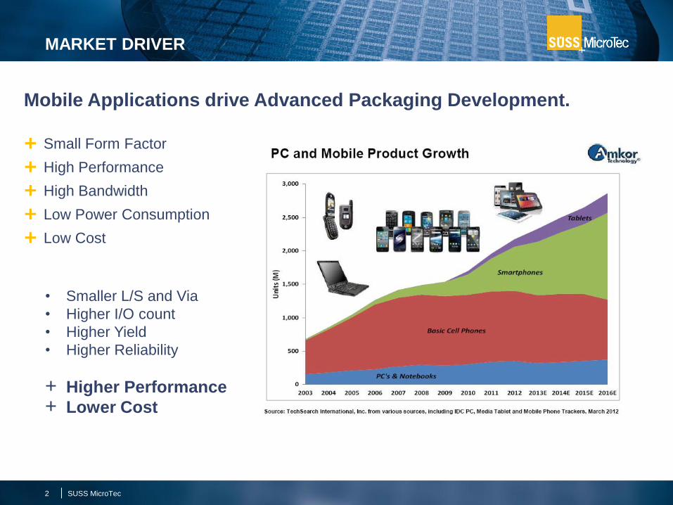
MARKET DRIVER
2
Mobile Applications drive Advanced Packaging Development.
Small Form Factor
High Performance
High Bandwidth
Low Power Consumption
Low Cost
• Smaller L/S and Via
• Higher I/O count
• Higher Yield
• Higher Reliability
+ Higher Performance
+ Lower Cost
SUSS MicroTec
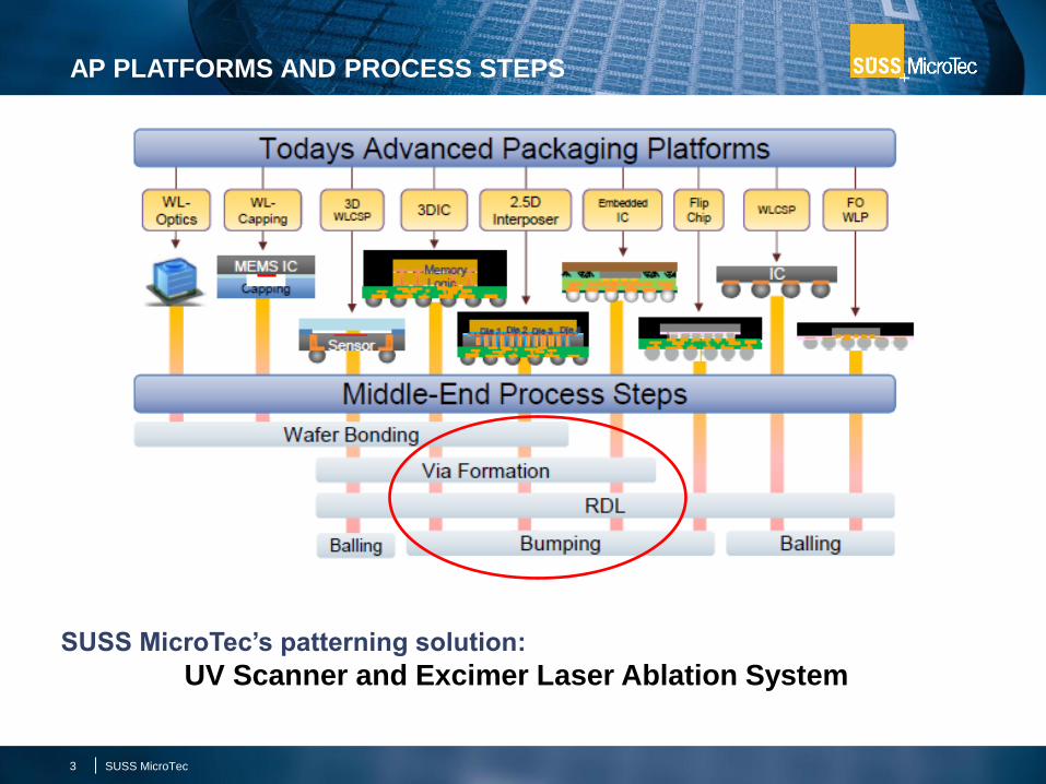
AP PLATFORMS AND PROCESS STEPS
SUSS MicroTec 3
SUSS MicroTec’s patterning solution:
UV Scanner and Excimer Laser Ablation System
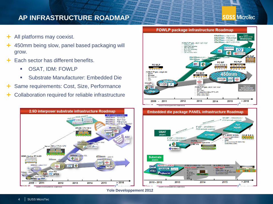
AP INFRASTRUCTURE ROADMAP
4 SUSS MicroTec
All platforms may coexist.
450mm being slow, panel based packaging will
grow.
Each sector has different benefits.
OSAT, IDM: FOWLP
Substrate Manufacturer: Embedded Die
Same requirements: Cost, Size, Performance
Collaboration required for reliable infrastructure
Yole Developpement 2012
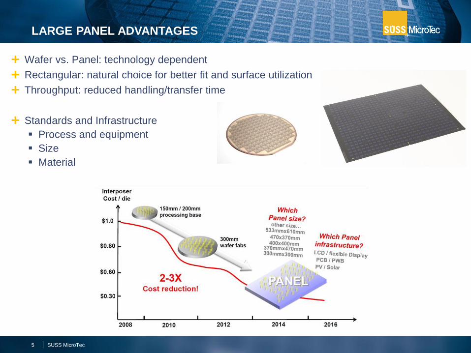
Wafer vs. Panel: technology dependent
Rectangular: natural choice for better fit and surface utilization
Throughput: reduced handling/transfer time
Standards and Infrastructure
Process and equipment
Size
Material
LARGE PANEL ADVANTAGES
SUSS MicroTec 5
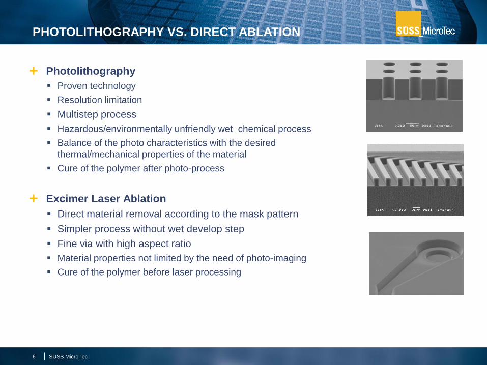
Photolithography
Proven technology
Resolution limitation
Multistep process
Hazardous/environmentally unfriendly wet chemical process
Balance of the photo characteristics with the desired
thermal/mechanical properties of the material
Cure of the polymer after photo-process
Excimer Laser Ablation
Direct material removal according to the mask pattern
Simpler process without wet develop step
Fine via with high aspect ratio
Material properties not limited by the need of photo-imaging
Cure of the polymer before laser processing
PHOTOLITHOGRAPHY VS. DIRECT ABLATION
6 SUSS MicroTec
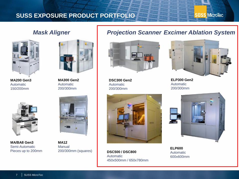
SUSS EXPOSURE PRODUCT PORTFOLIO
7
MA300 Gen2
Automatic
200/300mm
MA/BA8 Gen3
Semi-Automatic
Pieces up to 200mm
MA200 Gen3
Automatic
150/200mm
MA12
Manual
200/300mm (squares)
DSC300 Gen2
Automatic
200/300mm
ELP300 Gen2
Automatic
200/300mm
Mask Aligner Projection Scanner Excimer Ablation System
DSC500 / DSC800
Automatic
450x500mm / 650x780mm
ELP600
Automatic
600x600mm
SUSS MicroTec
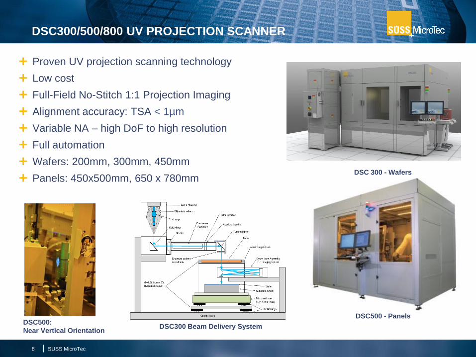
DSC300/500/800 UV PROJECTION SCANNER
8 SUSS MicroTec
Proven UV projection scanning technology
Low cost
Full-Field No-Stitch 1:1 Projection Imaging
Alignment accuracy: TSA < 1µm
Variable NA – high DoF to high resolution
Full automation
Wafers: 200mm, 300mm, 450mm
Panels: 450x500mm, 650 x 780mm DSC 300 - Wafers
DSC500 - Panels DSC500:
Near Vertical Orientation DSC300 Beam Delivery System
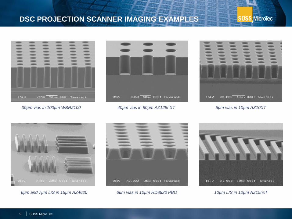
DSC PROJECTION SCANNER IMAGING EXAMPLES
9
30µm vias in 100µm WBR2100
10µm L/S in 12µm AZ15nxT
40µm vias in 80µm AZ125nXT 5µm vias in 10µm AZ10XT
6µm and 7µm L/S in 15µm AZ4620 6µm vias in 10µm HD8820 PBO
SUSS MicroTec
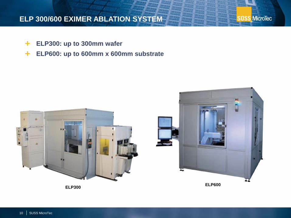
ELP 300/600 EXIMER ABLATION SYSTEM
10 SUSS MicroTec
ELP300: up to 300mm wafer
ELP600: up to 600mm x 600mm substrate
ELP300 ELP600
EXCIMER LASER ABLATION
11
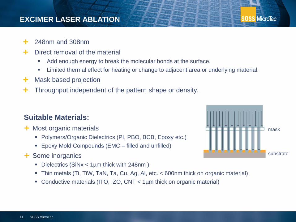
248nm and 308nm
Direct removal of the material
Add enough energy to break the molecular bonds at the surface.
Limited thermal effect for heating or change to adjacent area or underlying material.
Mask based projection
Throughput independent of the pattern shape or density.
Suitable Materials:
Most organic materials
Polymers/Organic Dielectrics (PI, PBO, BCB, Epoxy etc.)
Epoxy Mold Compounds (EMC – filled and unfilled)
Some inorganics
Dielectrics (SiNx < 1µm thick with 248nm )
Thin metals (Ti, TiW, TaN, Ta, Cu, Ag, Al, etc. < 600nm thick on organic material)
Conductive materials (ITO, IZO, CNT < 1µm thick on organic material)
SUSS MicroTec
mask
substrate
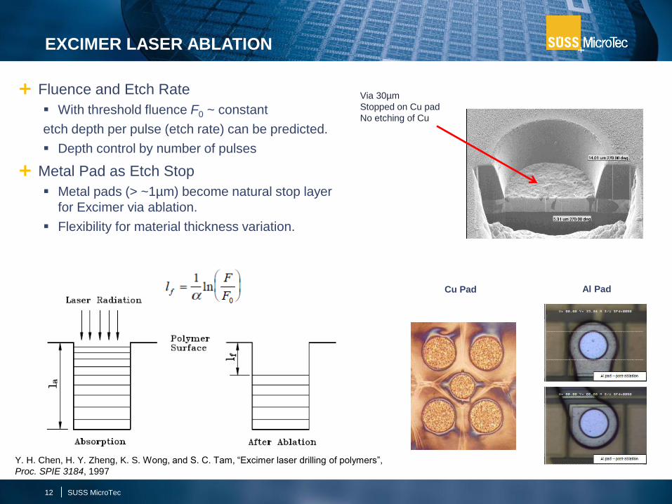
Fluence and Etch Rate
With threshold fluence F0 ~ constant
etch depth per pulse (etch rate) can be predicted.
Depth control by number of pulses
Metal Pad as Etch Stop
Metal pads (> ~1µm) become natural stop layer
for Excimer via ablation.
Flexibility for material thickness variation.
Cu Pad Al Pad
Via 30µm
Stopped on Cu pad
No etching of Cu
12
EXCIMER LASER ABLATION
SUSS MicroTec
Y. H. Chen, H. Y. Zheng, K. S. Wong, and S. C. Tam, “Excimer laser drilling of polymers”,
Proc. SPIE 3184, 1997
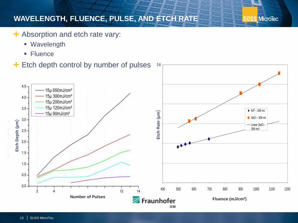
Polyimide Ablation Rate Dependence on Wavelength
0
0.1
0.2
0.3
0.4
0.5
0.6
400 500 600 700 800 900 1000 1100 1200
Fluence, mJ/cm²
Ab
latio
n r
ate, µ
m/p
uls
e
KrF – 248 nm
XeCl – 308 nm
Linear (XeCl –308 nm)Linear (KrF –248 nm)
WAVELENGTH, FLUENCE, PULSE, AND ETCH RATE
Absorption and etch rate vary:
Wavelength
Fluence
Etch depth control by number of pulses
SUSS MicroTec 13
Number of Pulses
E
tch
Dep
th (
μm
)
E
tch
Rate
(μ
m)
Fluence (mJ/cm2)
SIDE-WALL ANGLE AND FLUENCE
14 SUSS MicroTec
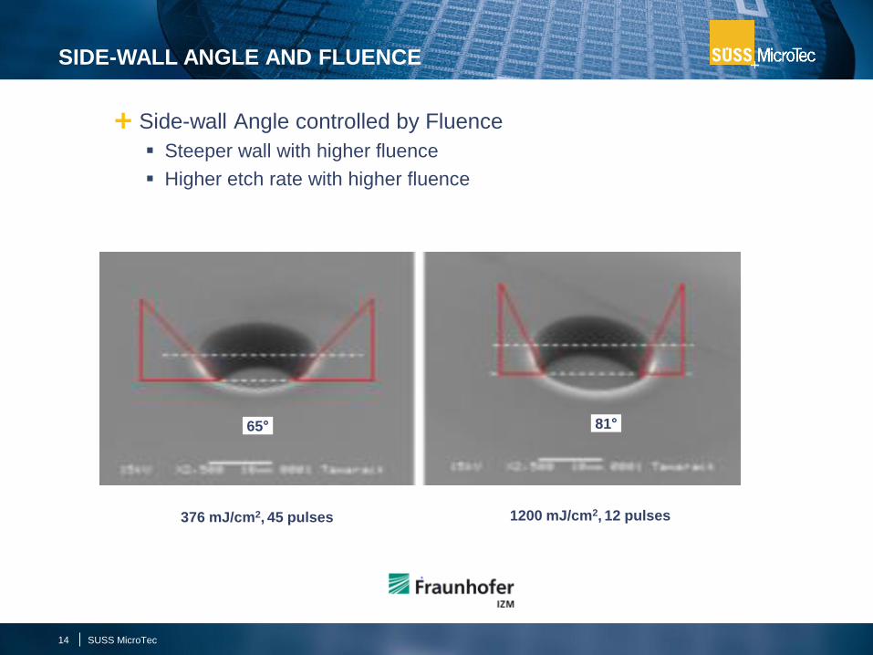
Side-wall Angle controlled by Fluence
Steeper wall with higher fluence
Higher etch rate with higher fluence
65° 81°
376 mJ/cm2, 45 pulses 1200 mJ/cm2, 12 pulses
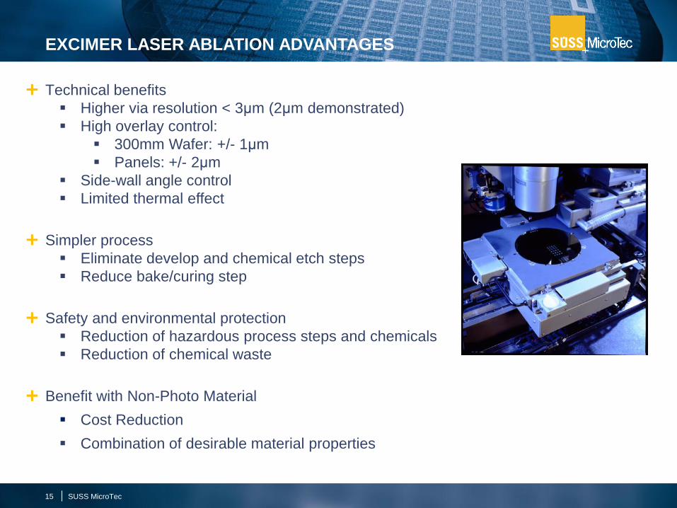
EXCIMER LASER ABLATION ADVANTAGES
15
Technical benefits
Higher via resolution < 3μm (2μm demonstrated)
High overlay control:
300mm Wafer: +/- 1μm
Panels: +/- 2μm
Side-wall angle control
Limited thermal effect
Simpler process
Eliminate develop and chemical etch steps
Reduce bake/curing step
Safety and environmental protection
Reduction of hazardous process steps and chemicals
Reduction of chemical waste
Benefit with Non-Photo Material
Cost Reduction
Combination of desirable material properties
SUSS MicroTec
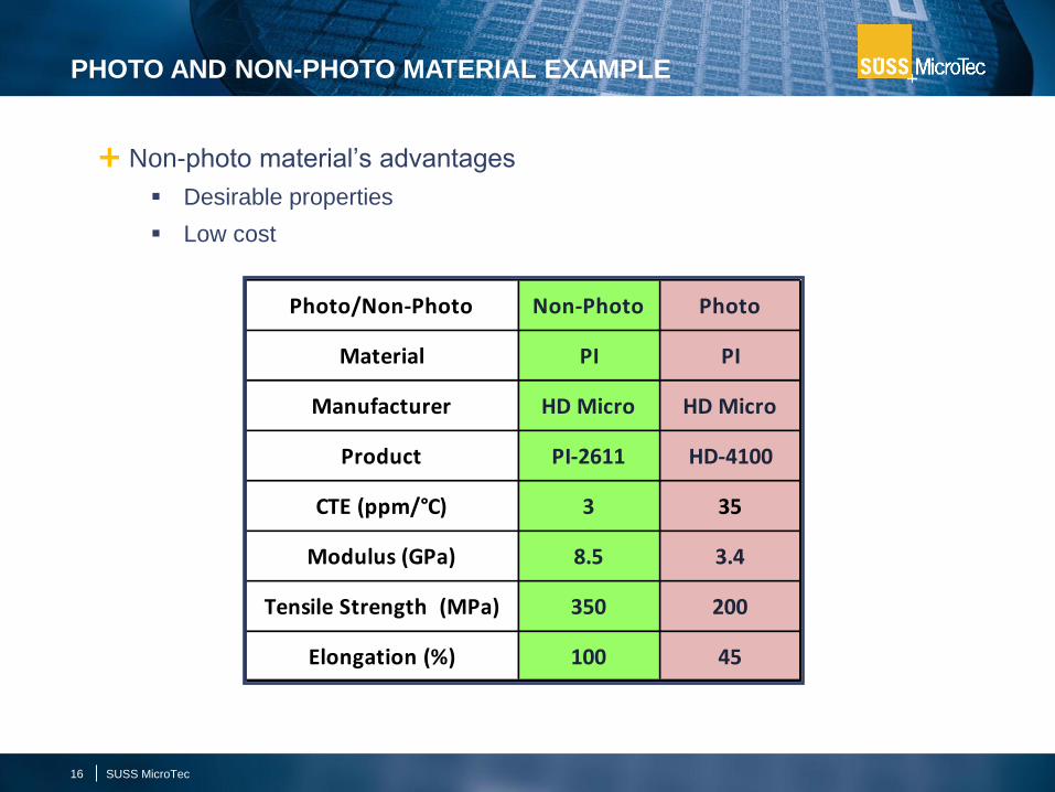
PHOTO AND NON-PHOTO MATERIAL EXAMPLE
16 SUSS MicroTec
Non-photo material’s advantages
Desirable properties
Low cost
Photo/Non-Photo Non-Photo Photo
Material PI PI
Manufacturer HD Micro HD Micro
Product PI-2611 HD-4100
CTE (ppm/°C) 3 35
Modulus (GPa) 8.5 3.4
Tensile Strength (MPa) 350 200
Elongation (%) 100 45
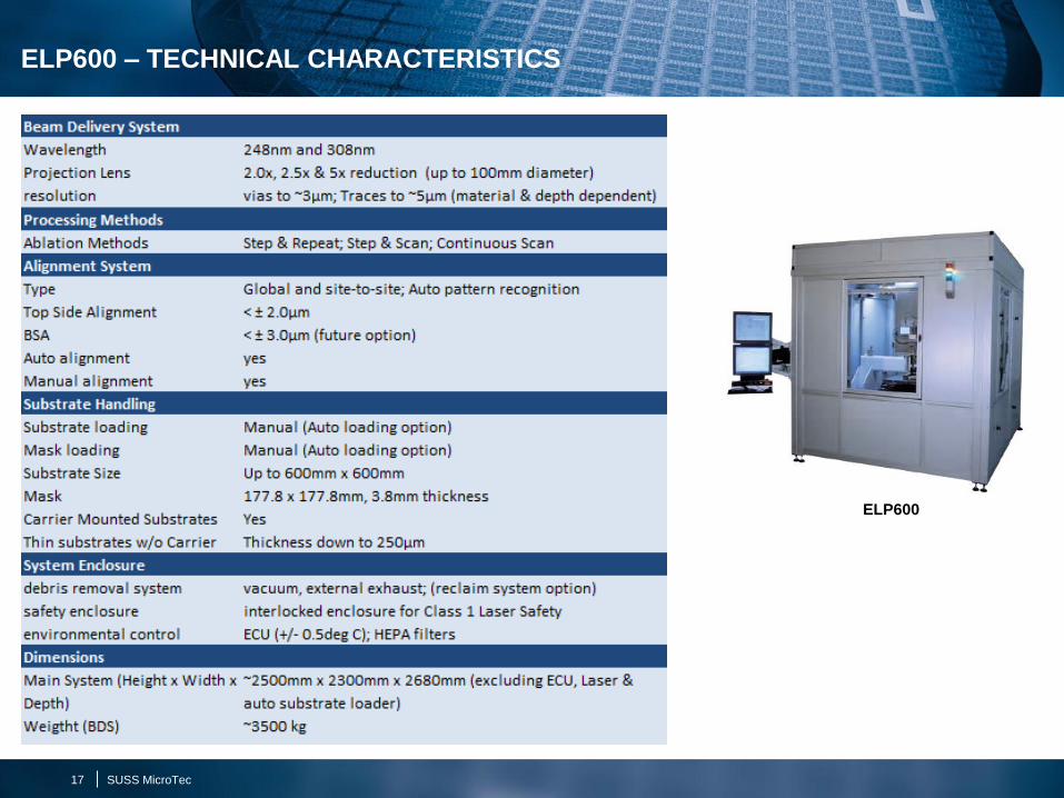
ELP600 – TECHNICAL CHARACTERISTICS
17 SUSS MicroTec
ELP600
18
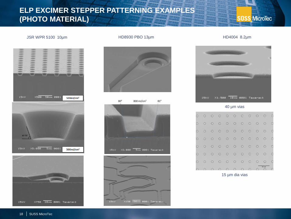
HD8930 PBO 13µm JSR WPR 5100 10µm HD4004 8.2µm
15 µm dia vias
40 µm vias
SUSS MicroTec
ELP EXCIMER STEPPER PATTERNING EXAMPLES
(PHOTO MATERIAL)
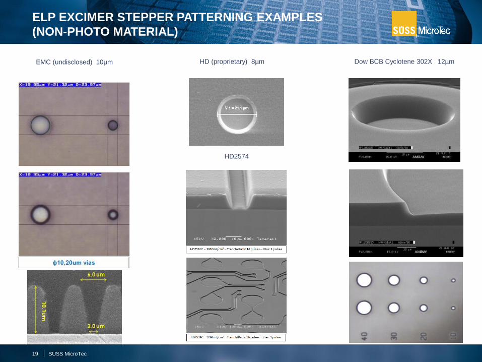
HD (proprietary) 8µm EMC (undisclosed) 10µm
ELP EXCIMER STEPPER PATTERNING EXAMPLES
(NON-PHOTO MATERIAL)
19 SUSS MicroTec
Dow BCB Cyclotene 302X 12µm
HD2574
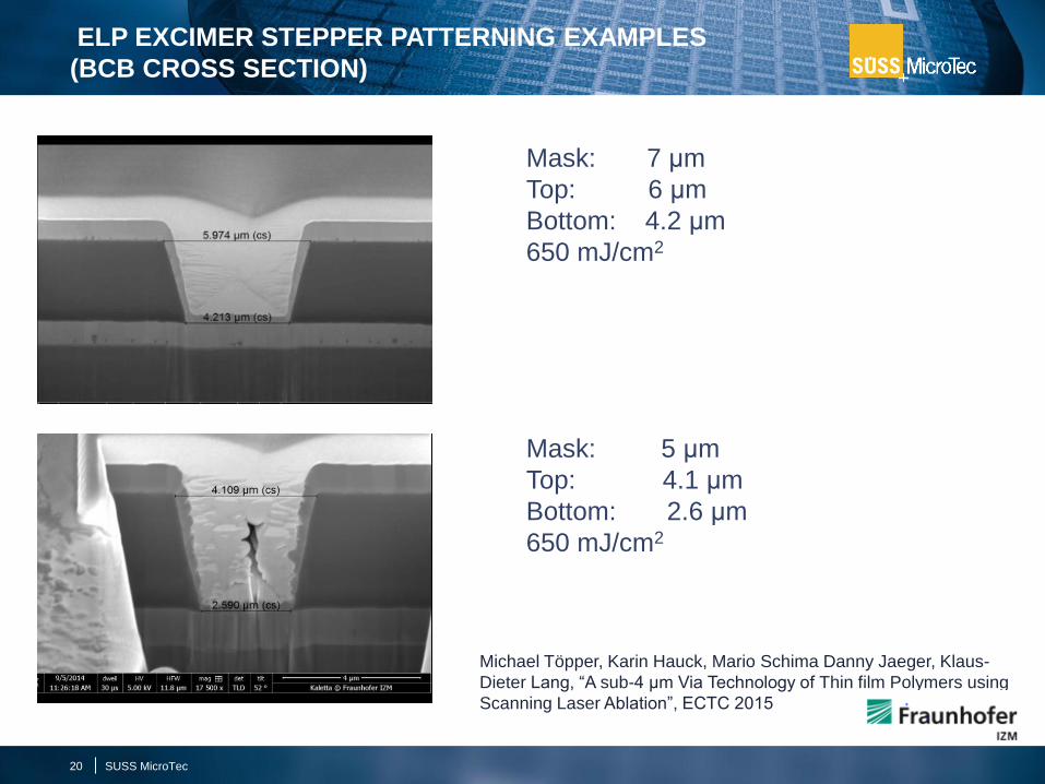
ELP EXCIMER STEPPER PATTERNING EXAMPLES
(BCB CROSS SECTION)
20
Mask: 7 μm
Top: 6 μm
Bottom: 4.2 μm
650 mJ/cm2
SUSS MicroTec
Mask: 5 μm
Top: 4.1 μm
Bottom: 2.6 μm
650 mJ/cm2
Michael Töpper, Karin Hauck, Mario Schima Danny Jaeger, Klaus-
Dieter Lang, “A sub-4 μm Via Technology of Thin film Polymers using
Scanning Laser Ablation”, ECTC 2015
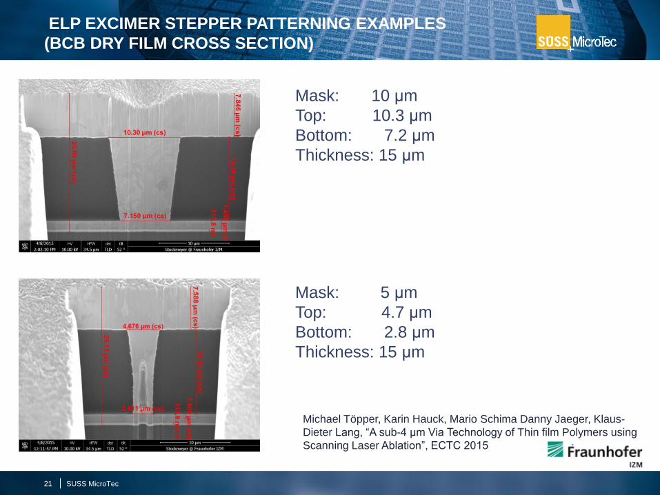
21
Mask: 10 μm
Top: 10.3 μm
Bottom: 7.2 μm
Thickness: 15 μm
SUSS MicroTec
Mask: 5 μm
Top: 4.7 μm
Bottom: 2.8 μm
Thickness: 15 μm
Michael Töpper, Karin Hauck, Mario Schima Danny Jaeger, Klaus-
Dieter Lang, “A sub-4 μm Via Technology of Thin film Polymers using
Scanning Laser Ablation”, ECTC 2015
ELP EXCIMER STEPPER PATTERNING EXAMPLES
(BCB DRY FILM CROSS SECTION)
ELP EXCIMER STEPPER PATTERNING EXAMPLES
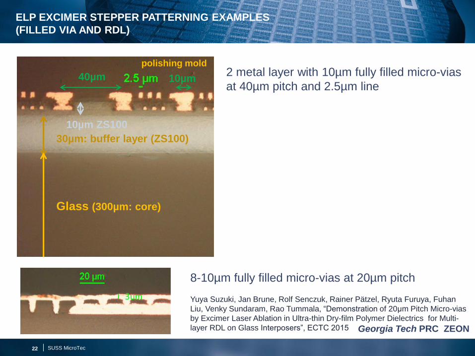
(FILLED VIA AND RDL)
polishing mold
10µm ZS100
30µm: buffer layer (ZS100)
Glass (300µm: core)
10µm 40µm 2 metal layer with 10µm fully filled micro-vias
at 40µm pitch and 2.5µm line
SUSS MicroTec 22
8-10µm fully filled micro-vias at 20µm pitch
Yuya Suzuki, Jan Brune, Rolf Senczuk, Rainer Pätzel, Ryuta Furuya, Fuhan
Liu, Venky Sundaram, Rao Tummala, “Demonstration of 20μm Pitch Micro-vias
by Excimer Laser Ablation in Ultra-thin Dry-film Polymer Dielectrics for Multi-
layer RDL on Glass Interposers”, ECTC 2015 Georgia Tech PRC ZEON
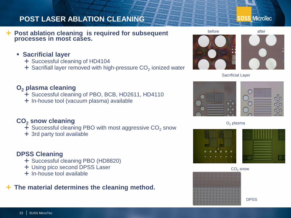
Post ablation cleaning is required for subsequent processes in most cases.
Sacrificial layer Successful cleaning of HD4104 Sacrifiall layer removed with high-pressure CO2 ionized water
O2 plasma cleaning Successful cleaning of PBO, BCB, HD2611, HD4110 In-house tool (vacuum plasma) available
CO2 snow cleaning Successful cleaning PBO with most aggressive CO2 snow 3rd party tool available
DPSS Cleaning Successful cleaning PBO (HD8820) Using pico second DPSS Laser In-house tool available
The material determines the cleaning method.
POST LASER ABLATION CLEANING
23 SUSS MicroTec
before after
Sacrificial Layer
O2 plasma
CO2 snow
DPSS
Mobile products drive packaging trend
Cost, Form Factor, Performance, Yield
Large size rectangular panel will grow for high volume manufacturing.
Driven by cost reduction
Patterning is a major factor along with material development.
Suss MicroTec provides Mask Aligner, UV Projection Scanner and Excimer Laser
Ablation for patterning applications.
UV scanner and excimer laser stepper are available for large format patterning.
Excimer laser stepper provides maximum benefits with non-photo materials.
Excimer laser stepper applications in RDL Via and Trench formation,
SLR and Laser Debonding.
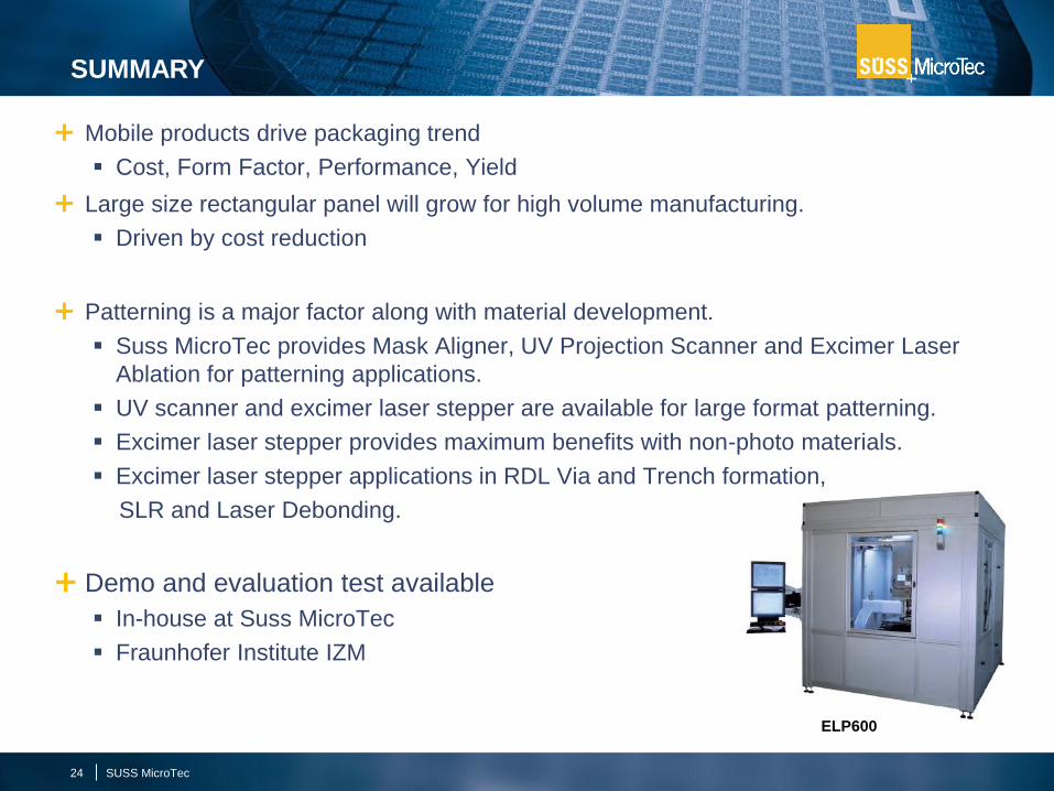
Demo and evaluation test available
In-house at Suss MicroTec
Fraunhofer Institute IZM
SUMMARY
24 SUSS MicroTec
ELP600

SUSS MicroTec 25