Embed Size (px)
Citation preview

CNT Based Solar CellsMAE C187L
Joyce ChenKari HarrisonKyle Martinez

Our Approach
• An array of micro-sized “blocks” composed of single walled carbon nanotubes coated with photovoltaic materials and anti-reflective coating on a silicon wafer
• The 3 dimensional surface causes light rays to be trapped inside the cell
• This, combined with the anti-reflective surface reduces the percentage of reflected rays

Our Approach

Methodology
• The single walled nanotubes are cheaper, easier to fabricate and have better electrical properties than multi walled nanotubes
• Silicon based photovoltaic materials are cheaper than many alternatives, and proven to be successful and reliable
• E-beam lithography and chemical vapor deposition were used where applicable because we are familiar with these processes

Step 1: Silicon wafer

Step 1: Silicon wafer
• Clean a 2 inch silicon wafer with Acetone, Methanol and IPA
• De-ionized water rinse
• N2 blow dry

Step 2a: E-beam Lithography:Spin Coating Photoresist

Step 2a: E-beam Lithography:Spin Coating Photoresist
• PMMA 495C2: 500 RPM for 5 seconds and 4000 RPM for 45 seconds
• Soft bake Sample at 180C for 90 seconds

Step 2b: E-beam Lithography:E-beam Patterning

Step 2b: E-beam Lithography:E-beam Patterning
• Make a pattern of 700 blocks x 700 blocks of 40um x 40um squares with 10 um gaps
• Based on our limited knowledge, we would use the same parameters procedure as in Lab 1

Step 2c: E-beam Lithography:Metal Deposition

Step 2c: E-beam Lithography:Metal Deposition
• Using chemical vapor deposition we would deposit a thin layer of iron oxide on top of the patterned resist and wafer

Step 2d: E-beam Lithography:Photoresist Development and Metal Lift-Off

Step 2d: E-beam Lithography:Photoresist Development and Metal Lift-Off
• Soak PMMA developer for 30-40 sec– Isopropanol + MIBK at 3 to 1 volume ratio
• Rinse in Isopropanol
• Blow dry with N2
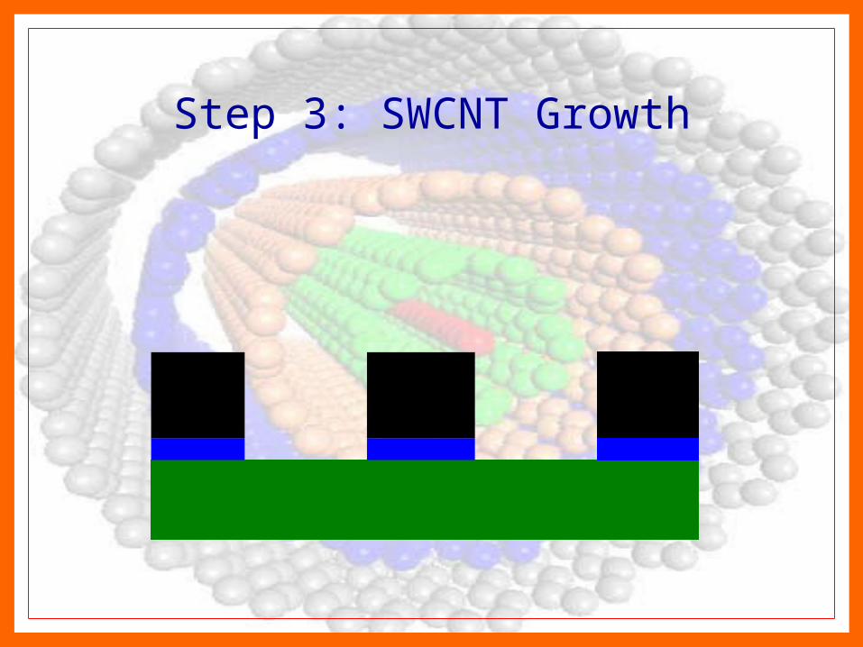
Step 3: SWCNT Growth

Step 3: SWCNT Growth
• Place the wafer in a furnace heated to 1000C and pass an argon flow through the furnace
• Replace the argon flow with a methane flow of 99% purity at a flow rate of 6150cm3/min under 1.25 atm for 10 minutes
• Replace the methane flow with an argon flow and cool to room temperature

Step 4: Photovoltaic Deposition

Step 4: Photovoltaic Deposition
• Using molecular beam epitaxy, deposit silicon phosphorus (n-type layer) and silicon boron (p-type layer)
• Molecular beam epitaxy is a slow deposition of films taking place in a high vacuum

Step 5: Anti-Reflective Coating Deposition

Step 5: Anti-Reflective Coating Deposition
• Use a Cooke Thermal Evaporator to deposit a layer of silicon monoxide on the solar cell
• Program the Sigma Film Thickness mOnitor with these parameters– Density = 2.13 g/cm3
– Tooling = 126%– Z-ratio = 0.87

Step 5: Anti-Reflective Coating Deposition
• Fill a long tungsten boat with SiO fragments• Turn power up to 15% until boat beings to
glow and stay there for 2 minutes• Switch on heating until and increase dial to
30% for 30 seconds, until deposition rate is between 0.3-0.5 angstroms/s
• Slowly increase to 35%-40%• Once desirable thickness is obtained, close
shutter and record thickness after 1 minute• Slowly reduce boat current to zero and switch
of heating unit

Cost Analysis
• Iron Oxide $1.00/ounce• Silicon ~ $2.00/lb• Silicon monoxide ~ $1.45/g• Methane < $0.10/L• A typical solar cell costs ~$0.05/kwh• This cell uses less silicon, an expensive
commodity, and should produce more energy per square meter – therefore we would expect it to cost at least the same, if not less per kwh

Estimated Efficiency
• A similar experiment obtained a 7% efficiency, while it is expected that a 40% efficiency is possible
• The addition of an anti-reflective coating can reduce the reflected light from 30% to 10%, which adds ~ 1% efficiency

Lifespan
• Current solar panels are rated ~ 30 years• It is still unknown how long carbon nanotubes
will last, but we assume their lifespan is the same as the copper wires they are replacing, if not longer
• This would make our solar cell life span also ~30 years

Testing
• Test in lab with UV light to determine kw per square meter
• Test at different angles to the sun to determine the correct incident angle for maximum efficiency
• Test in extreme temperatures, as well as in wind tunnels to determine structural stability

References
http://www.gtri.gatech.edu/casestudy/3d-solar-cells-boost-efficiency
http://www.nanowerk.com/news/newsid=1763.php
http://www.alfa.com/en/ge100w.pgm
http://ostc.physics.uiowa.edu/~microfab/manuals/pdf/deposition-SiO.pdf
http://blog.sciencenet.cn/upload/blog/file/2010/2/20102193247668823.pdf
http://en.wikipedia.org/wiki/Photovoltaic_array
http://en.wikipedia.org/wiki/Carbon_nanotubes_in_photovoltaics
http://www.metalprices.com/FreeSite/metals/nickelalloy/nickelalloy.asp
Lecture Slides and Lab Handouts