Embed Size (px)
Citation preview
1
CS/ECE 5710/6710
CMOS Processing
Copyright © 2011 Pearson Education, Inc. Publishing as Pearson Addison-Wesley
2
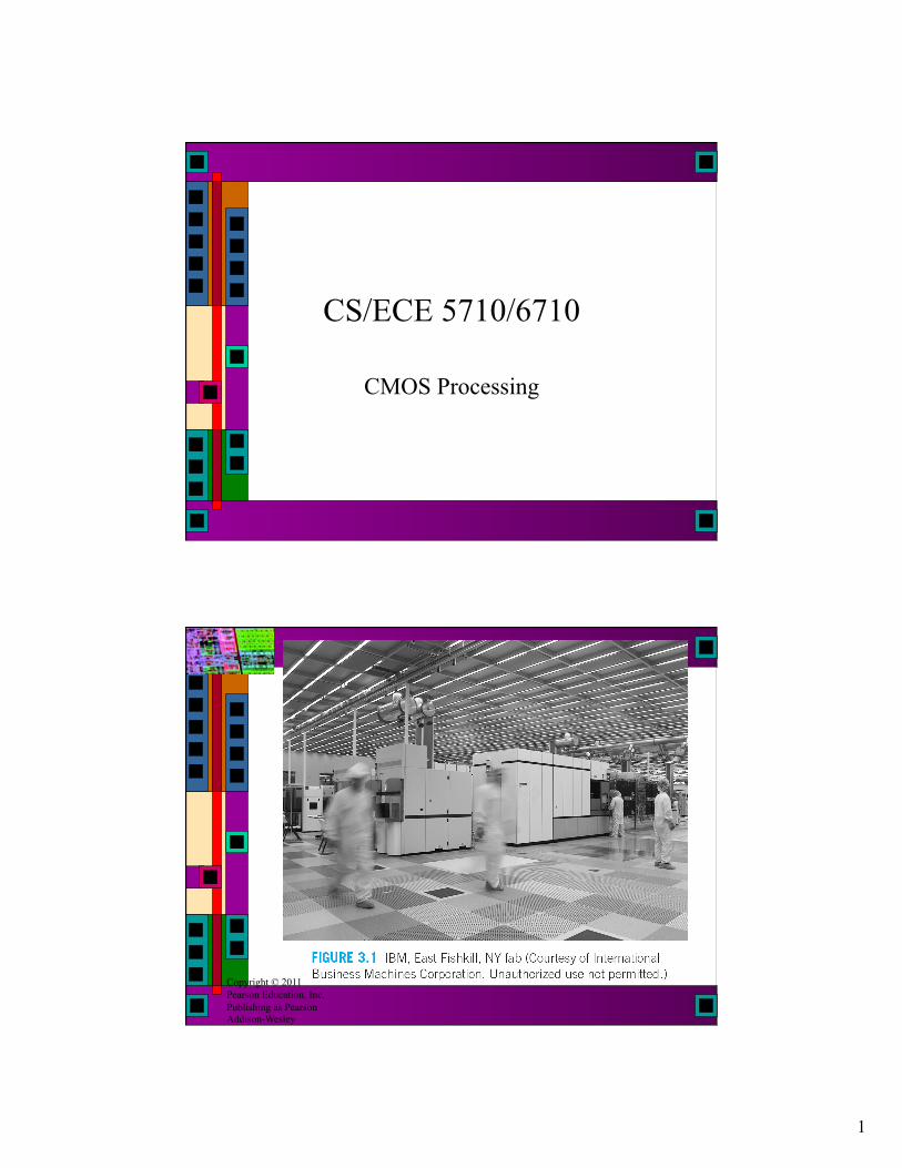
N-type Transistor
+
-
i electrons Vds
+Vgs S
G
D
N-type from the top
Top view shows patterns that make up the transistor
3
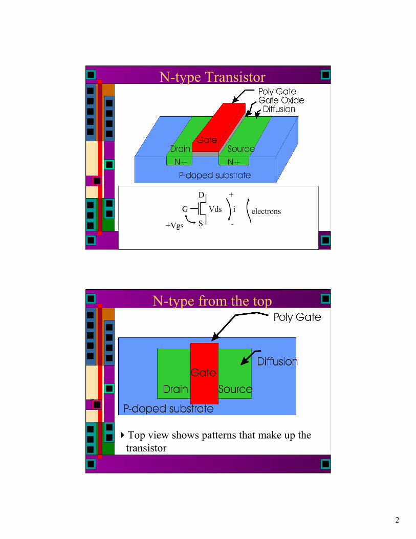
Diffusion Mask
Mask for just the diffused regions
Polysilicon Mask
Mask for just the polysilicon areas
4
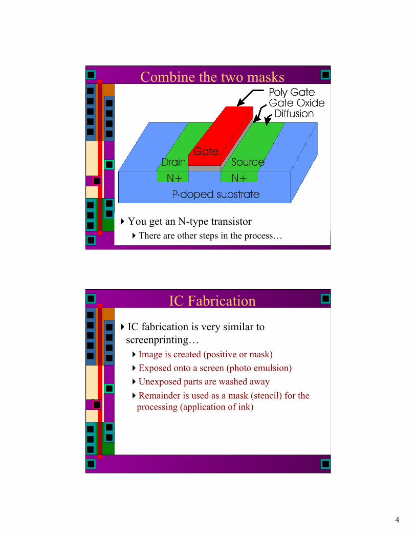
Combine the two masks
You get an N-type transistor There are other steps in the process…
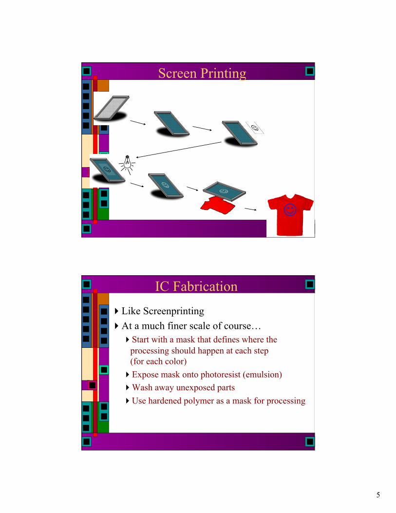
IC Fabrication IC fabrication is very similar to
screenprinting… Image is created (positive or mask) Exposed onto a screen (photo emulsion) Unexposed parts are washed away Remainder is used as a mask (stencil) for the
processing (application of ink)
5
Screen Printing
IC Fabrication Like Screenprinting At a much finer scale of course…
Start with a mask that defines where the processing should happen at each step (for each color)
Expose mask onto photoresist (emulsion) Wash away unexposed parts Use hardened polymer as a mask for processing
6
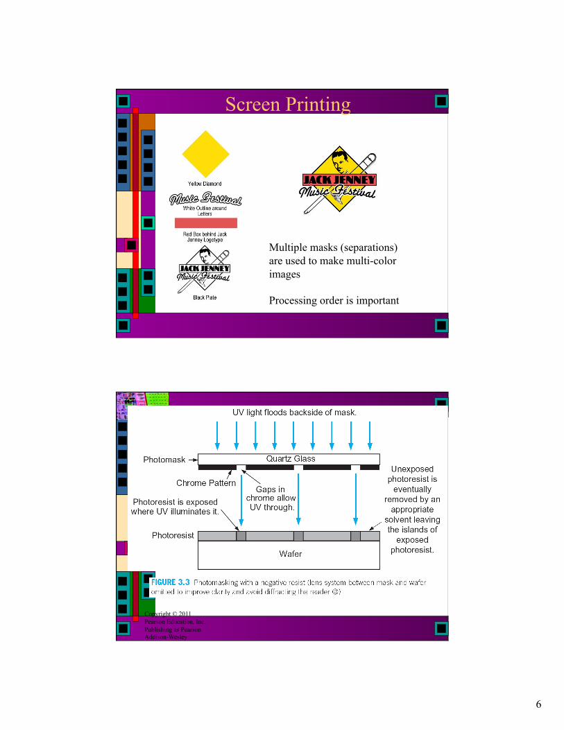
Screen Printing
Multiple masks (separations) are used to make multi-color images
Processing order is important
Copyright © 2011 Pearson Education, Inc. Publishing as Pearson Addison-Wesley
7
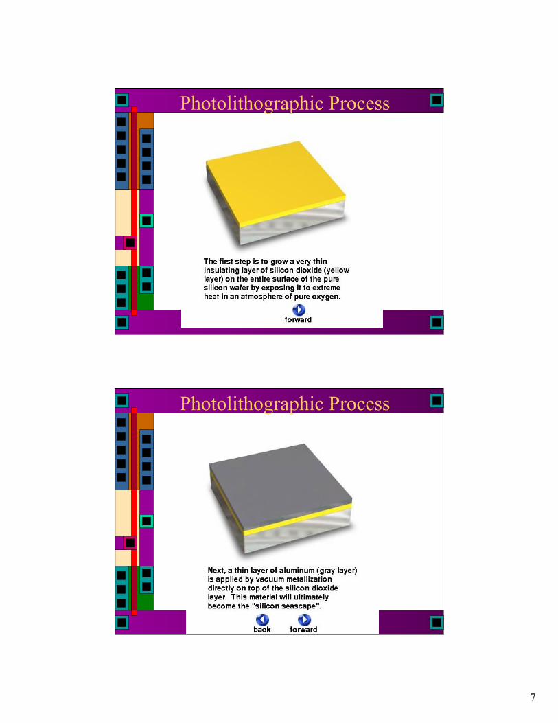
Photolithographic Process
Photolithographic Process
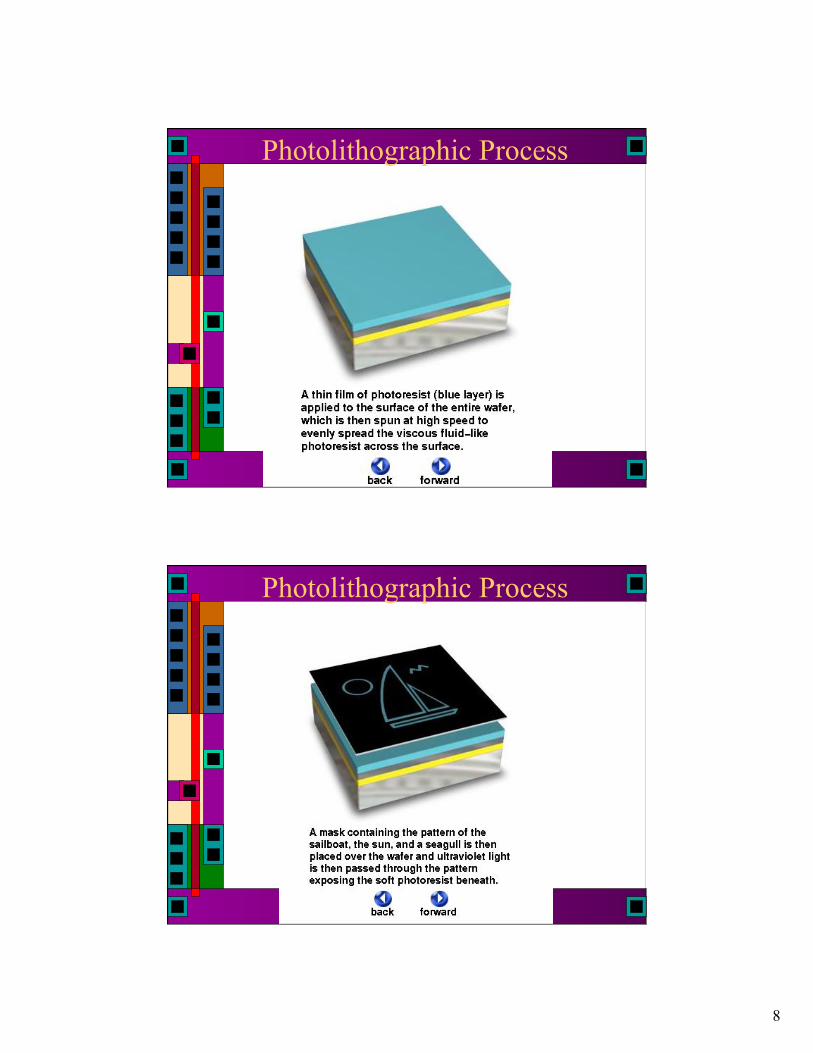
8
Photolithographic Process
Photolithographic Process
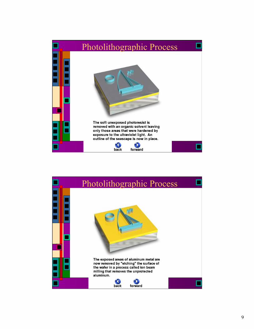
9
Photolithographic Process
Photolithographic Process
10
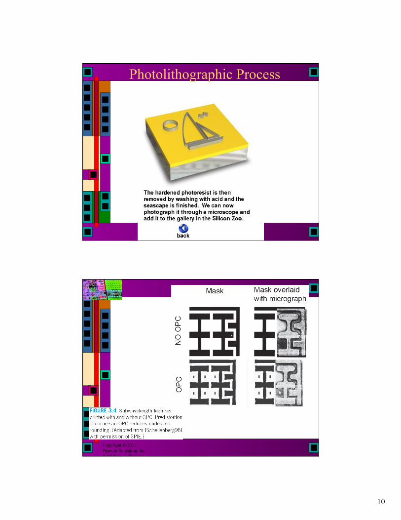
Photolithographic Process
Copyright © 2011 Pearson Education, Inc. Publishing as Pearson
11
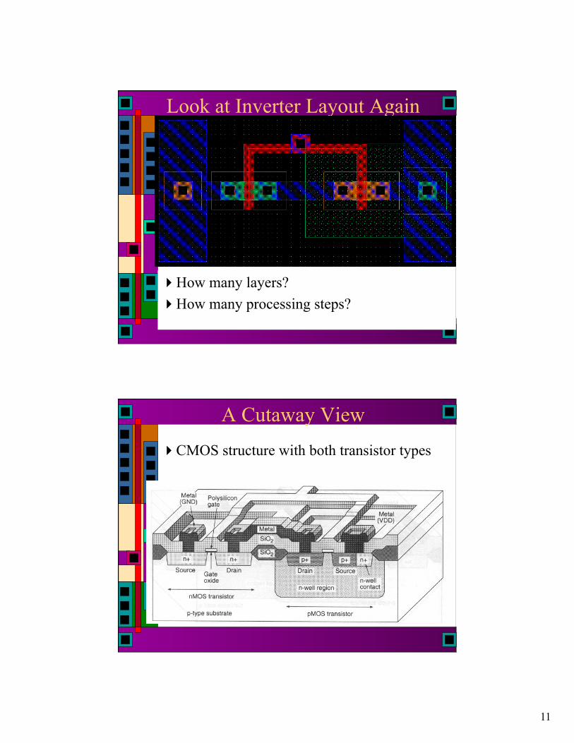
Look at Inverter Layout Again
How many layers? How many processing steps?
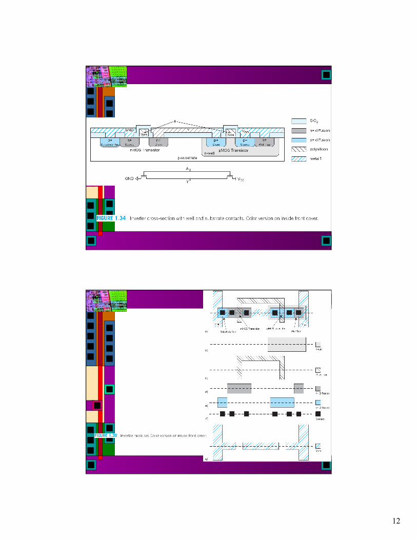
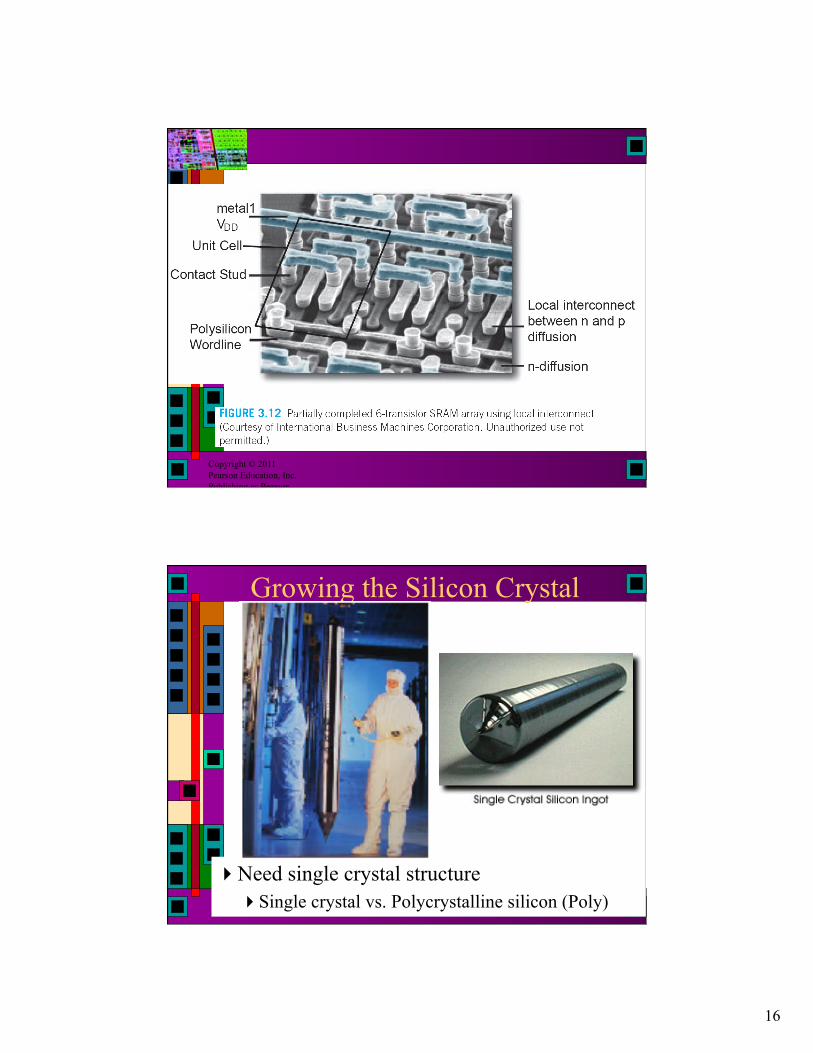
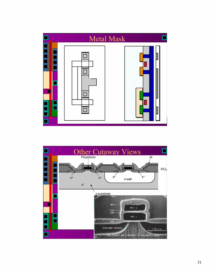
A Cutaway View CMOS structure with both transistor types
12
13
14
Copyright © 2011 Pearson Education, Inc. Publishing as Pearson Addison-Wesley
15
Copyright © 2011 Pearson Education, Inc. Publishing as Pearson Addison-Wesley
Copyright © 2011 Pearson Education, Inc. Publishing as Pearson
16
Copyright © 2011 Pearson Education, Inc. Publishing as Pearson
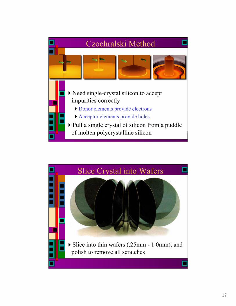
Growing the Silicon Crystal
Need single crystal structure Single crystal vs. Polycrystalline silicon (Poly)
17
Czochralski Method
Need single-crystal silicon to accept impurities correctly Donor elements provide electrons Acceptor elements provide holes
Pull a single crystal of silicon from a puddle of molten polycrystalline silicon
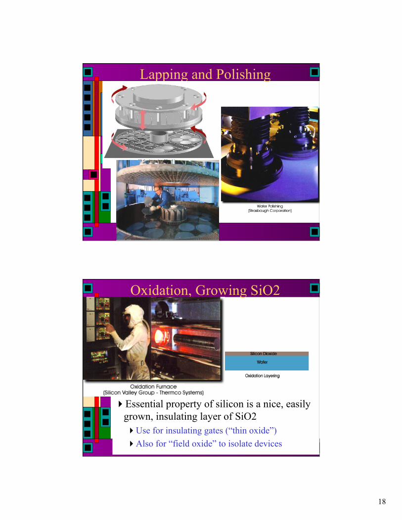
Slice Crystal into Wafers
Slice into thin wafers (.25mm - 1.0mm), and polish to remove all scratches
18
Lapping and Polishing
Oxidation, Growing SiO2
Essential property of silicon is a nice, easily grown, insulating layer of SiO2 Use for insulating gates (“thin oxide”) Also for “field oxide” to isolate devices
19
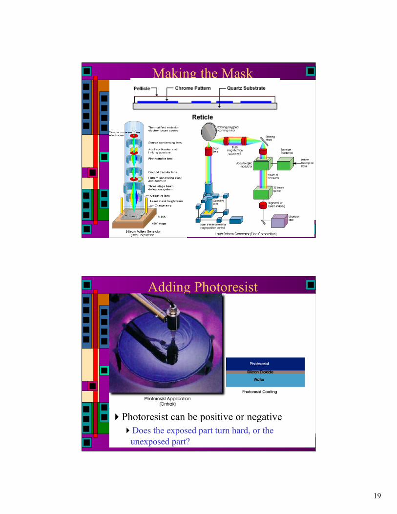
Making the Mask
Adding Photoresist
Photoresist can be positive or negative Does the exposed part turn hard, or the
unexposed part?
20
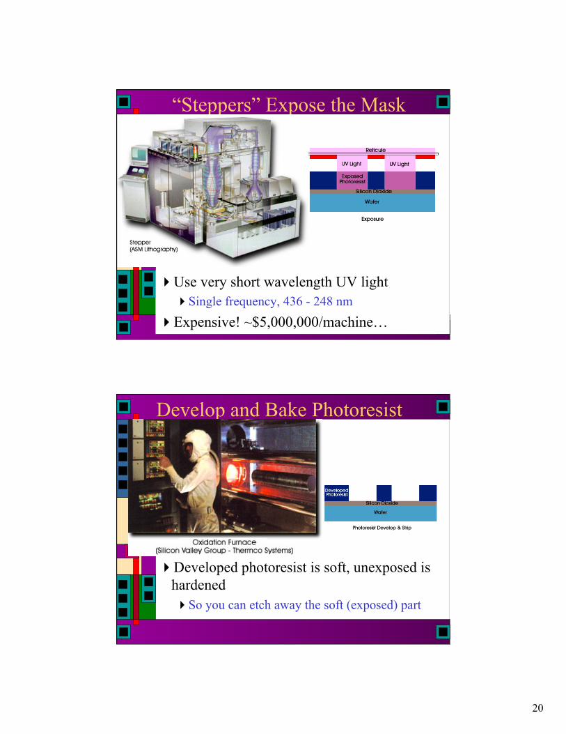
“Steppers” Expose the Mask
Use very short wavelength UV light Single frequency, 436 - 248 nm
Expensive! ~$5,000,000/machine…
Develop and Bake Photoresist
Developed photoresist is soft, unexposed is hardened So you can etch away the soft (exposed) part
21
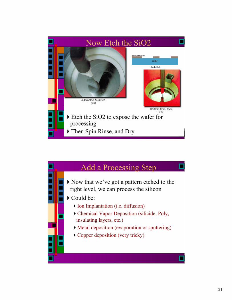
Now Etch the SiO2
Etch the SiO2 to expose the wafer for processing
Then Spin Rinse, and Dry
Add a Processing Step Now that we’ve got a pattern etched to the
right level, we can process the silicon Could be:
Ion Implantation (i.e. diffusion) Chemical Vapor Deposition (silicide, Poly,
insulating layers, etc.) Metal deposition (evaporation or sputtering) Copper deposition (very tricky)
22
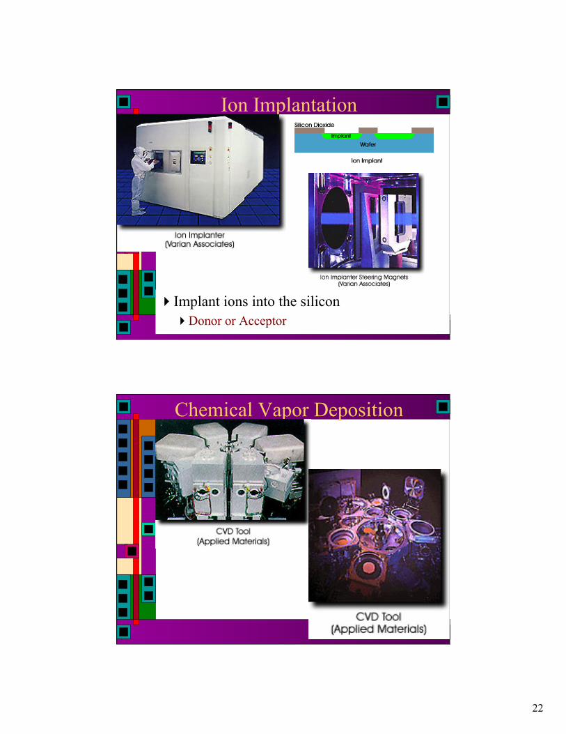
Ion Implantation
Implant ions into the silicon Donor or Acceptor
Chemical Vapor Deposition
23
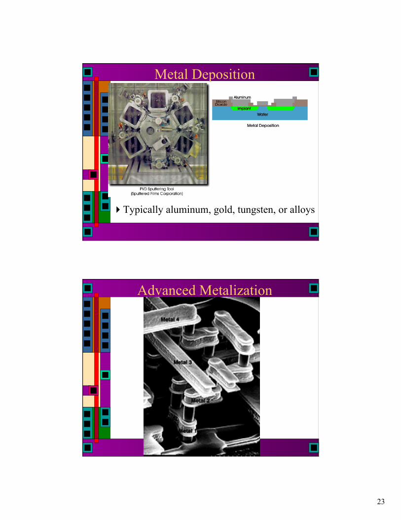
Metal Deposition
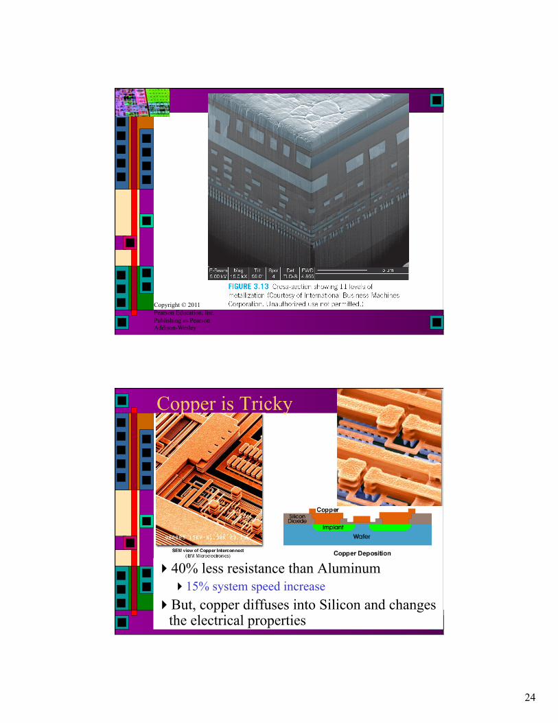
Typically aluminum, gold, tungsten, or alloys
Advanced Metalization
24
Copyright © 2011 Pearson Education, Inc. Publishing as Pearson Addison-Wesley
Copper is Tricky
40% less resistance than Aluminum 15% system speed increase
But, copper diffuses into Silicon and changes the electrical properties
25
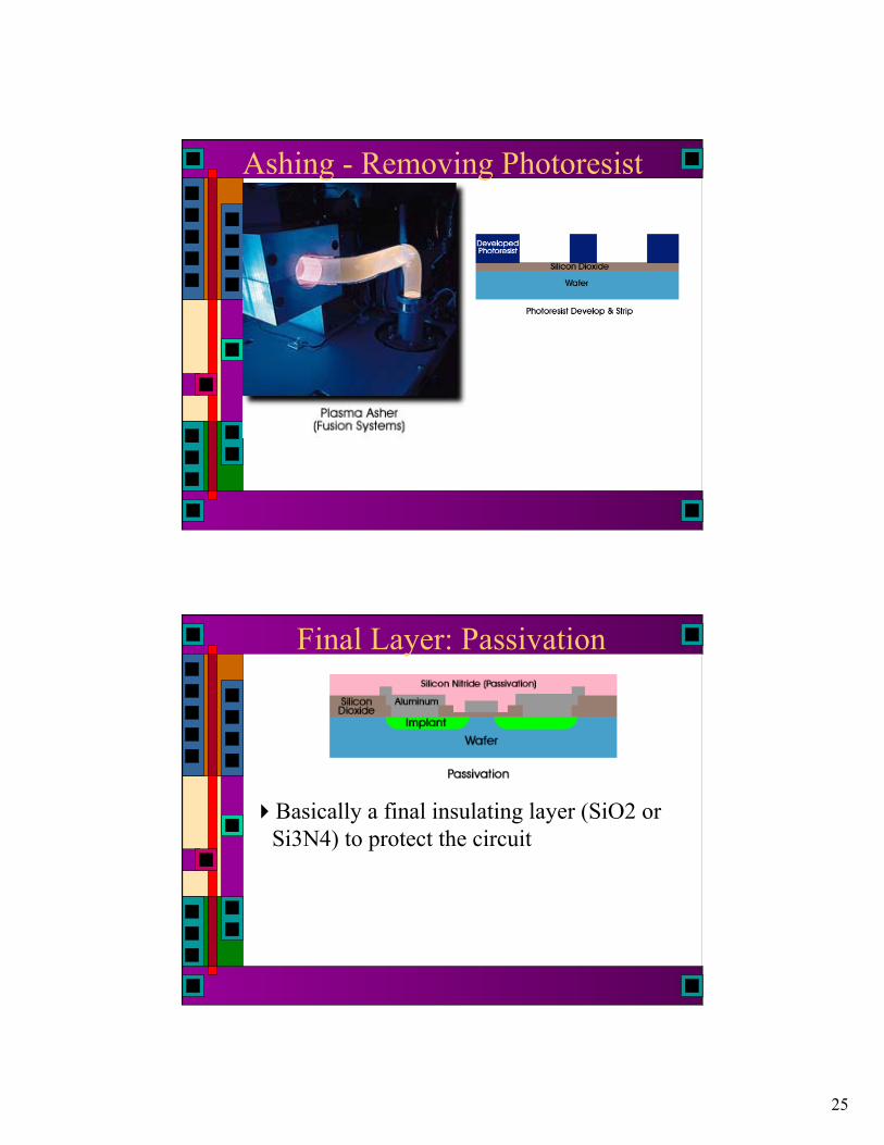
Ashing - Removing Photoresist
Final Layer: Passivation
Basically a final insulating layer (SiO2 or Si3N4) to protect the circuit
26
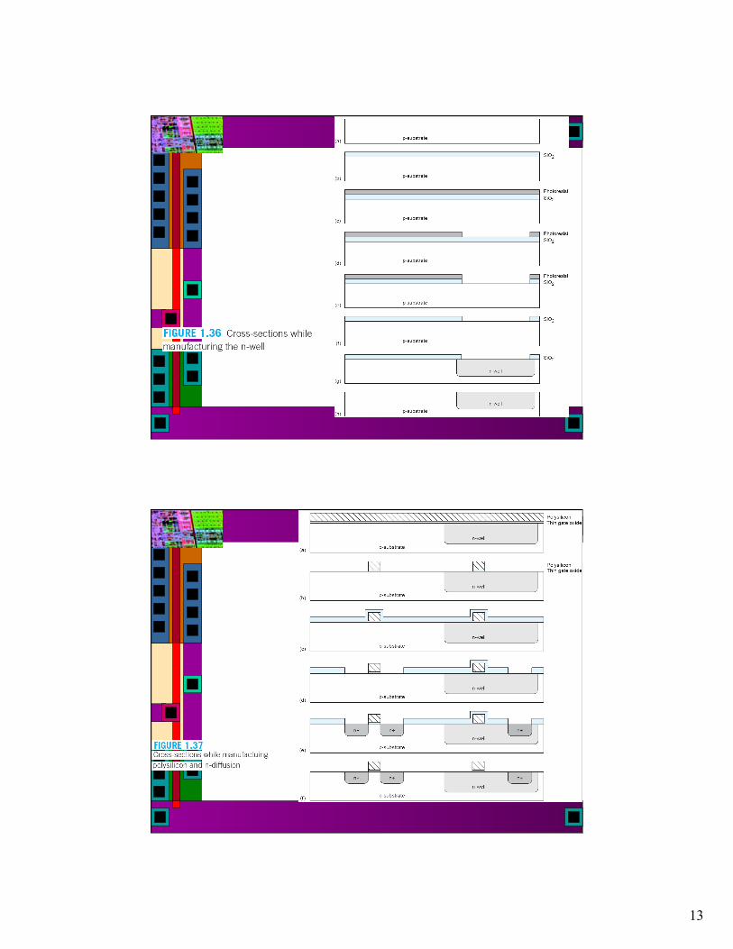
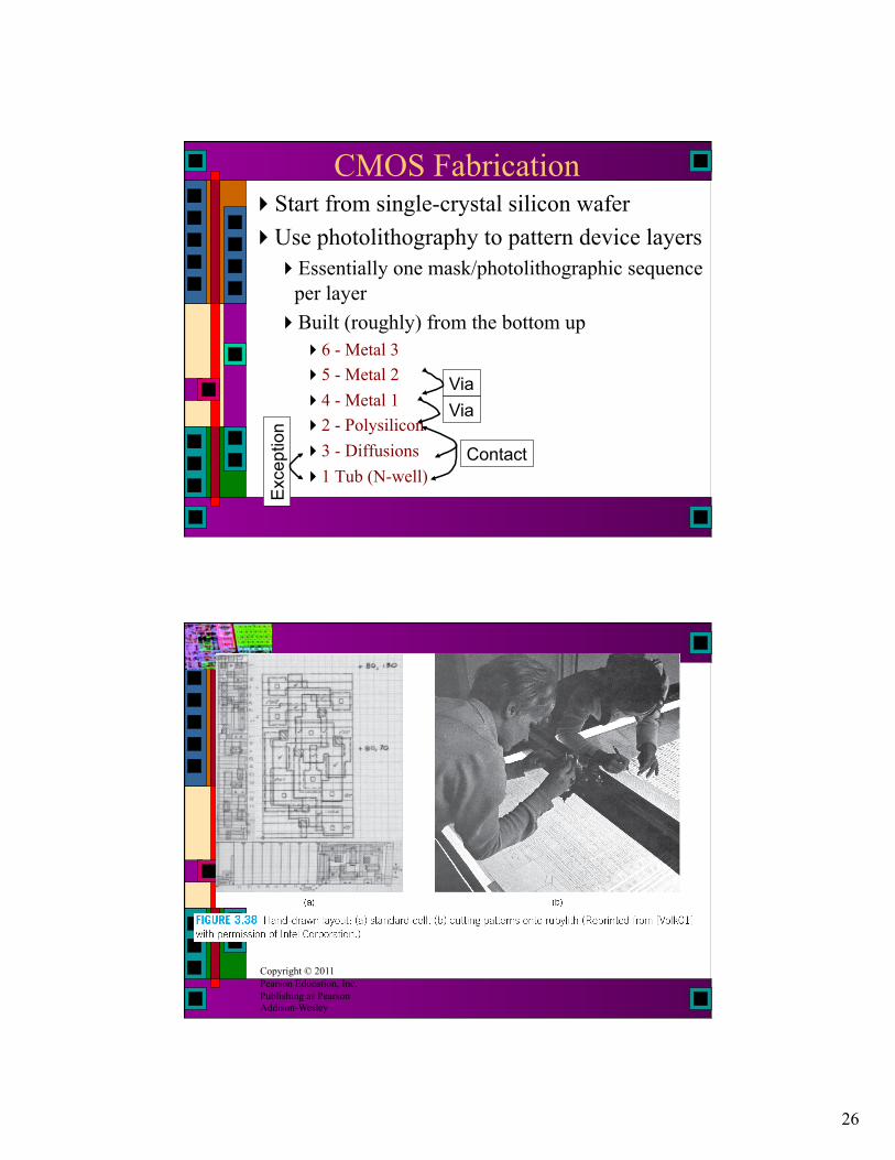
CMOS Fabrication Start from single-crystal silicon wafer Use photolithography to pattern device layers
Essentially one mask/photolithographic sequence per layer
Built (roughly) from the bottom up 6 - Metal 3 5 - Metal 2 4 - Metal 1 2 - Polysilicon 3 - Diffusions 1 Tub (N-well)
Exc
eptio
n
Contact
Via Via
Copyright © 2011 Pearson Education, Inc. Publishing as Pearson Addison-Wesley
27
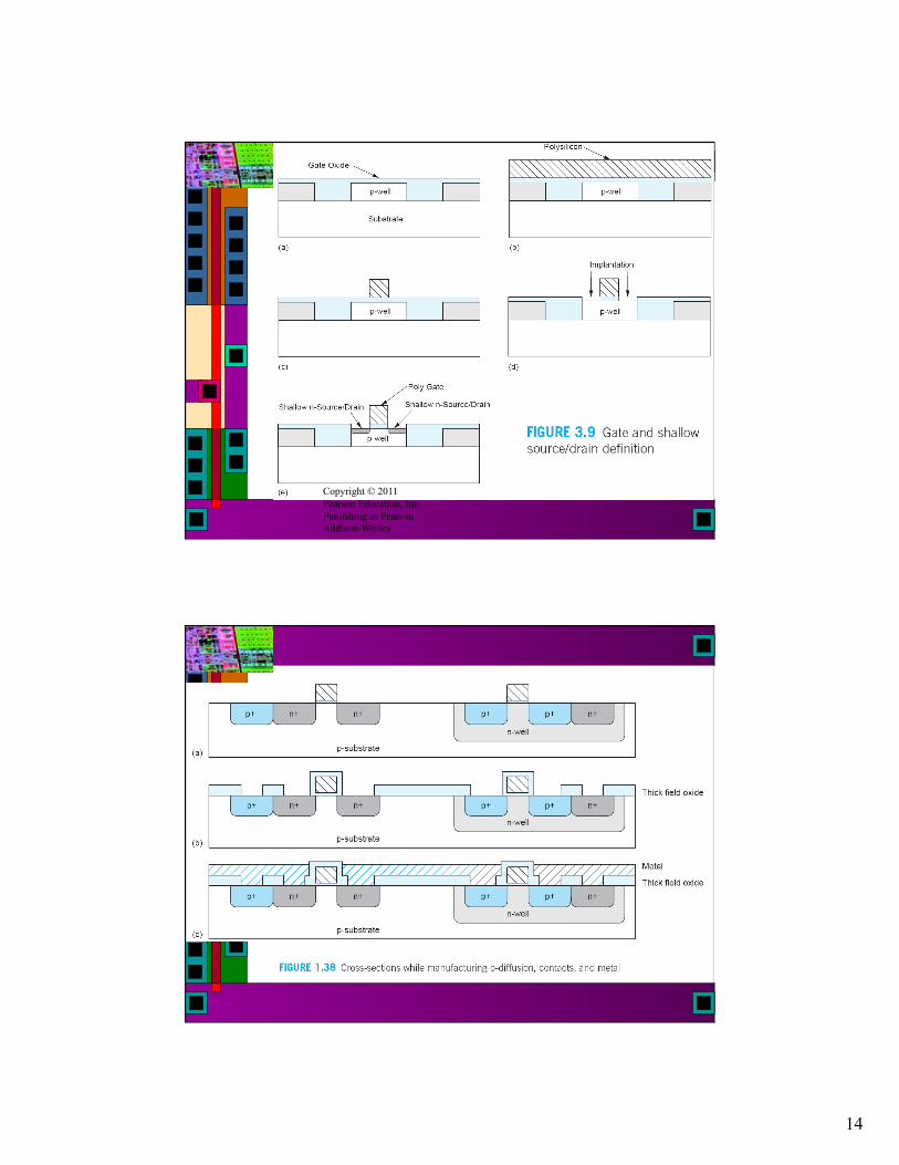
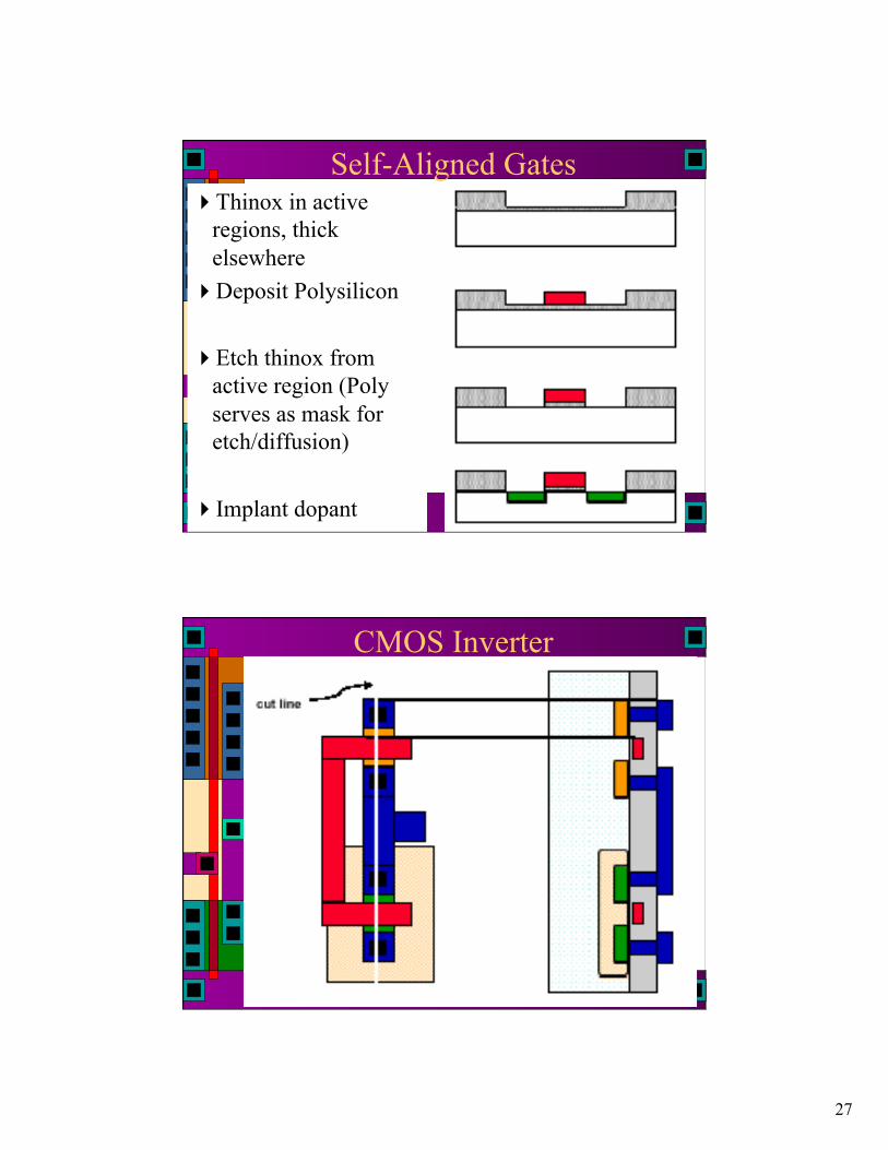
Self-Aligned Gates Thinox in active
regions, thick elsewhere
Deposit Polysilicon
Etch thinox from active region (Poly serves as mask for etch/diffusion)
Implant dopant
CMOS Inverter
28
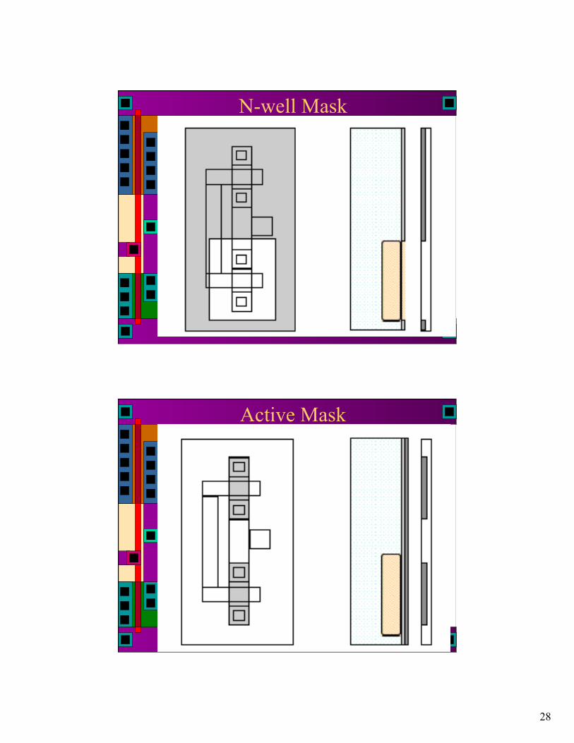
N-well Mask
Active Mask
29
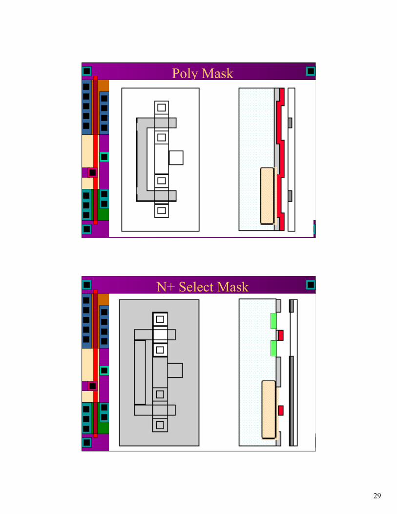
Poly Mask
N+ Select Mask
30
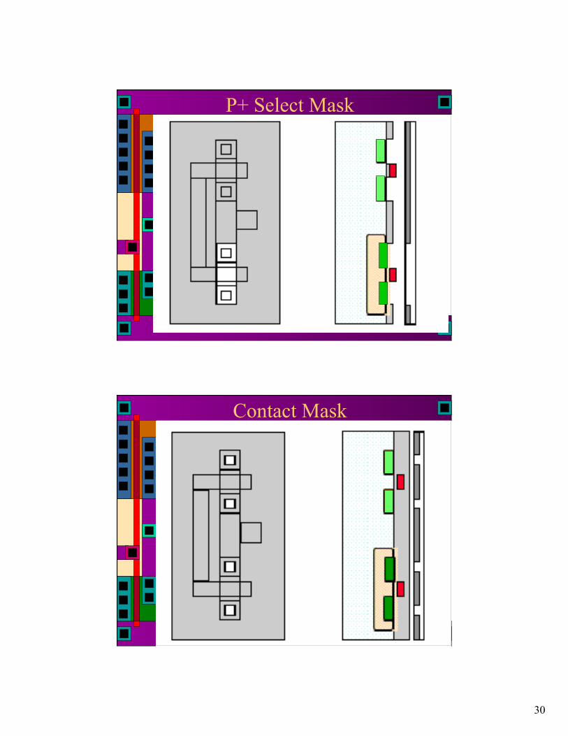
P+ Select Mask
Contact Mask
31
Metal Mask
Other Cutaway Views
32
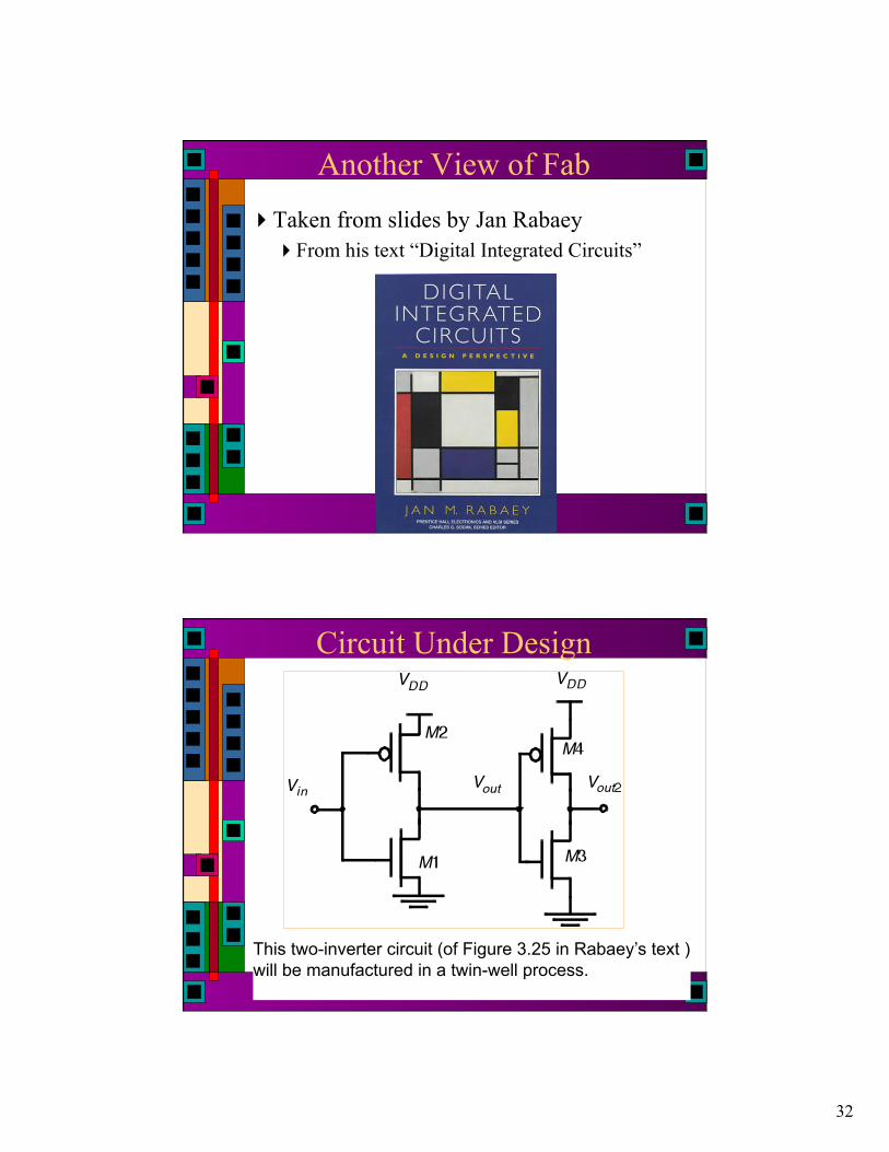
Another View of Fab Taken from slides by Jan Rabaey
From his text “Digital Integrated Circuits”
Circuit Under Design
This two-inverter circuit (of Figure 3.25 in Rabaey’s text ) will be manufactured in a twin-well process.
33
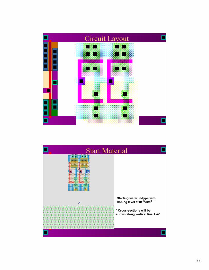
Circuit Layout
Start Material
Starting wafer: n-type with doping level = 10 13 /cm 3
* Cross-sections will be shown along vertical line A-A’
A
A’
34
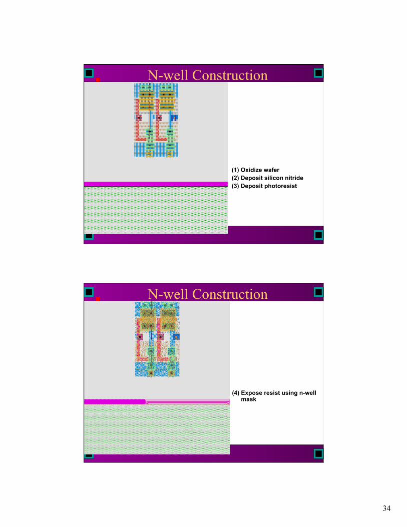
N-well Construction
(1) Oxidize wafer (2) Deposit silicon nitride (3) Deposit photoresist
N-well Construction
(4) Expose resist using n-well mask
35
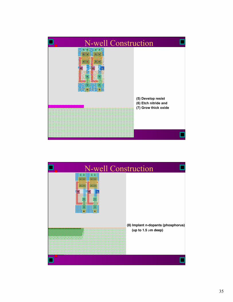
N-well Construction
(5) Develop resist (6) Etch nitride and (7) Grow thick oxide
N-well Construction
(8) Implant n-dopants (phosphorus) (up to 1.5 µ m deep)
36
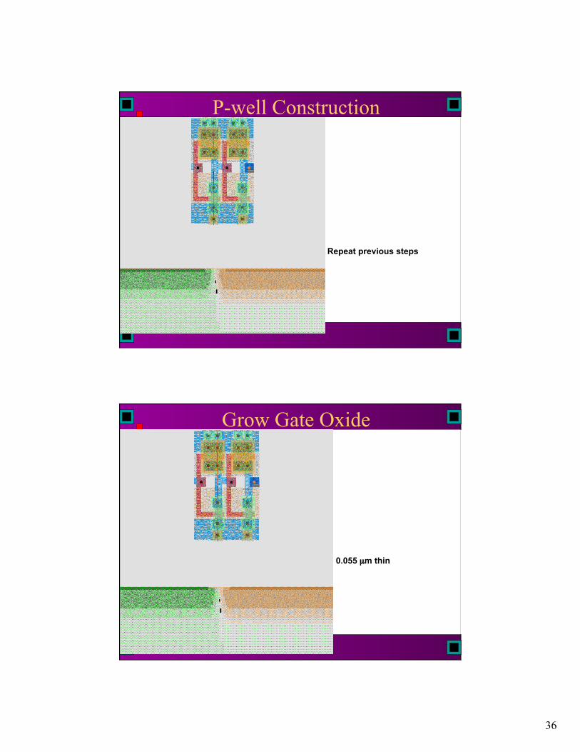
P-well Construction
Repeat previous steps
Grow Gate Oxide
0.055 µm thin
37
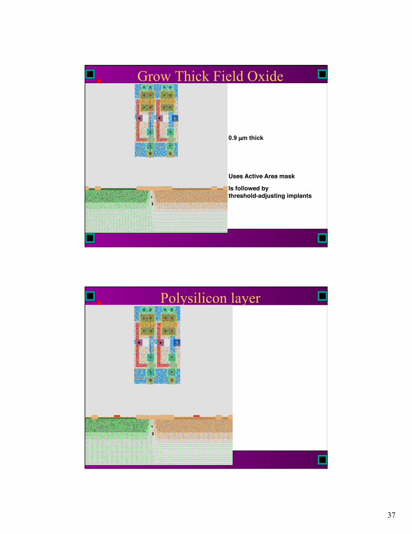
Grow Thick Field Oxide
Uses Active Area mask
Is followed by !threshold-adjusting implants
0.9 µm thick
Polysilicon layer
38
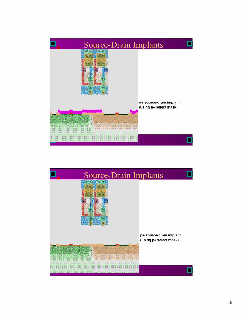
Source-Drain Implants
n+ source-drain implant (using n+ select mask)
Source-Drain Implants
p+ source-drain implant (using p+ select mask)
39
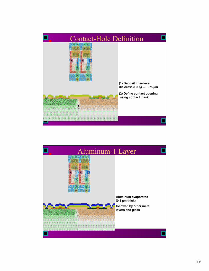
Contact-Hole Definition
(1) Deposit inter-level !dielectric (SiO2) — 0.75 µm
(2) Define contact opening! using contact mask
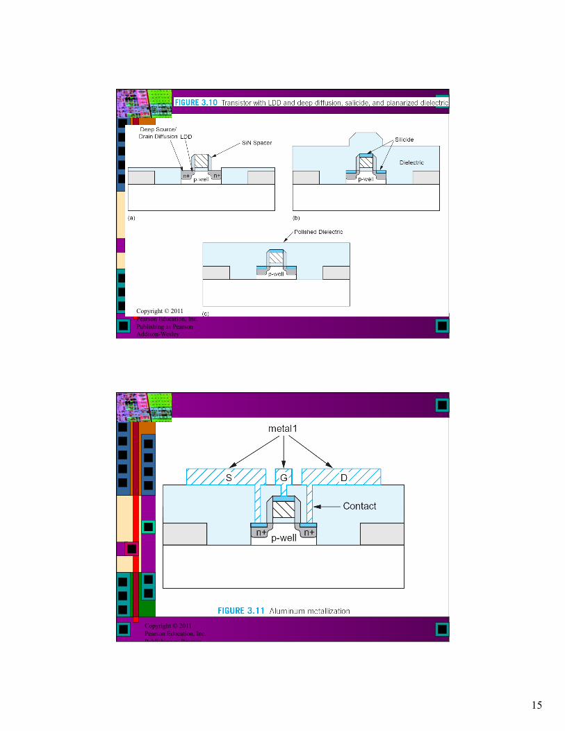
Aluminum-1 Layer
Aluminum evaporated !(0.8 µm thick) followed by other metal !layers and glass