Embed Size (px)
Citation preview


Closing the Power Gap between
ASIC and Custom
David Chinnery, Kurt Keutzer

3
Outline
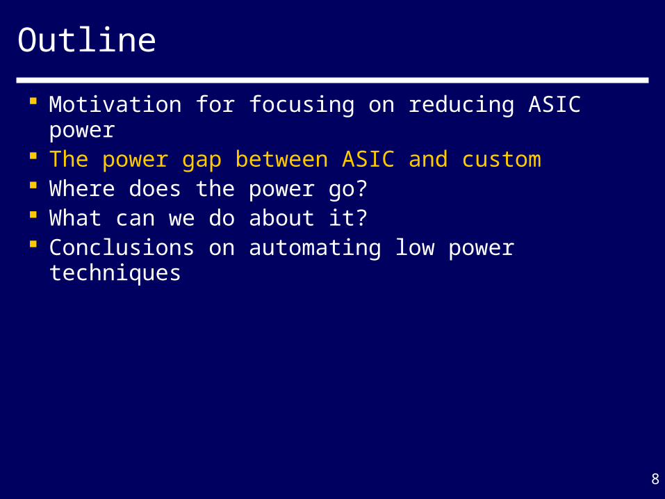
Motivation for focusing on reducing ASIC power The power gap between ASIC and custom Where does the power go? What can we do about it? Conclusions on automating low power techniques
4
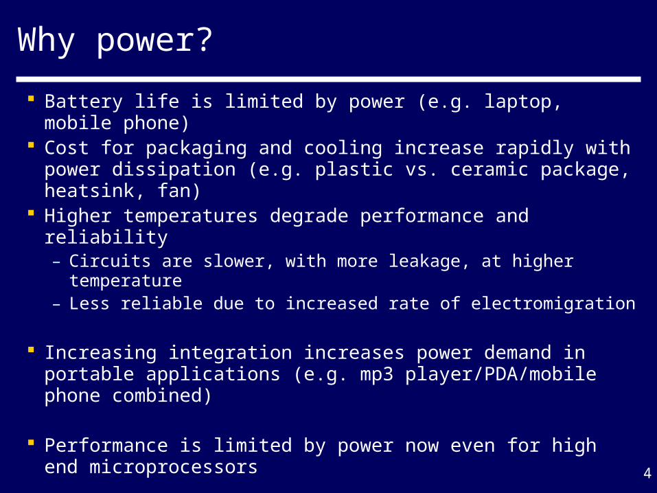
Why power?
Battery life is limited by power (e.g. laptop, mobile phone)
Cost for packaging and cooling increase rapidly with power dissipation (e.g. plastic vs. ceramic package, heatsink, fan)
Higher temperatures degrade performance and reliability– Circuits are slower, with more leakage, at higher
temperature– Less reliable due to increased rate of electromigration
Increasing integration increases power demand in portable applications (e.g. mp3 player/PDA/mobile phone combined)
Performance is limited by power now even for high end microprocessors

5
Power of high performance chips has increased
As device dimensions (W, L, Tox) scaled down by a factor k, for high performance, If supply Vdd and threshold
voltage Vth fixed, then power/unit area k3
If Vdd and Vth scaled downlinearly and , then power/unit area k0.7
Further voltage scaling may be limited …
Pow
er/
Un
it A
rea
(W/c
m2)
[Kuroda OYO BUTURI 2004]
100
10
1
digital signal processor
microprocessor
Vdd, V th
scaled
linearly with
dimensions
V dd, V
th
fixed
1
10
1000
Scaling Factor k (1/um)
data from ISSCC chips 1982-2002
6
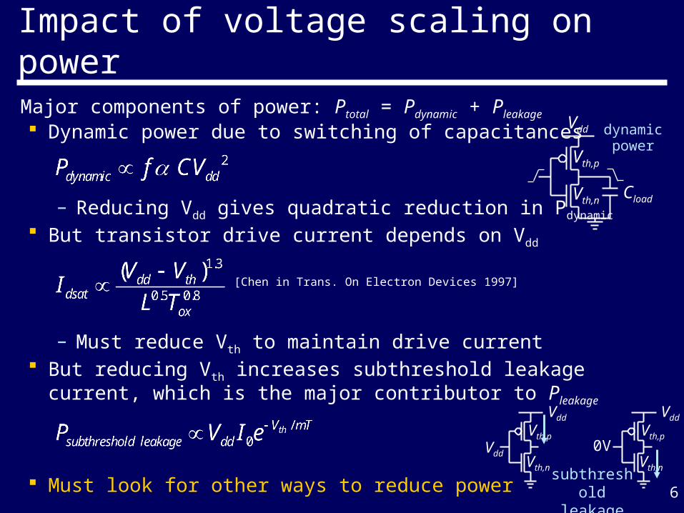
Impact of voltage scaling on power
Major components of power: Ptotal = Pdynamic + Pleakage
Dynamic power due to switching of capacitances
– Reducing Vdd gives quadratic reduction in Pdynamic
But transistor drive current depends on Vdd
– Must reduce Vth to maintain drive current But reducing Vth increases subthreshold leakage
current, which is the major contributor to Pleakage
Must look for other ways to reduce power
[Chen in Trans. On Electron Devices 1997]
Vdd
VddVth,n
Vth,p
Vdd
0VVth,n
Vth,p
subthresholdleakage
Vdd
Cload
Vth,p
Vth,n
dynamic power

7
Automate low power techniques
Custom designers can try to optimize the design at all levels
Electronic design automation (EDA) tools for ASICs– Most of the design optimization is high level– Fast time-to-market and lower design cost – Increasingly important to reduce design cost for larger
chips
What is the power gap between (automated) ASIC design and custom design?– We need to characterize the contributing factors– Can we close the power gap?
– Identify custom techniques that can be used in an EDA flow
8
Outline
Motivation for focusing on reducing ASIC power The power gap between ASIC and custom Where does the power go? What can we do about it? Conclusions on automating low power techniques
9
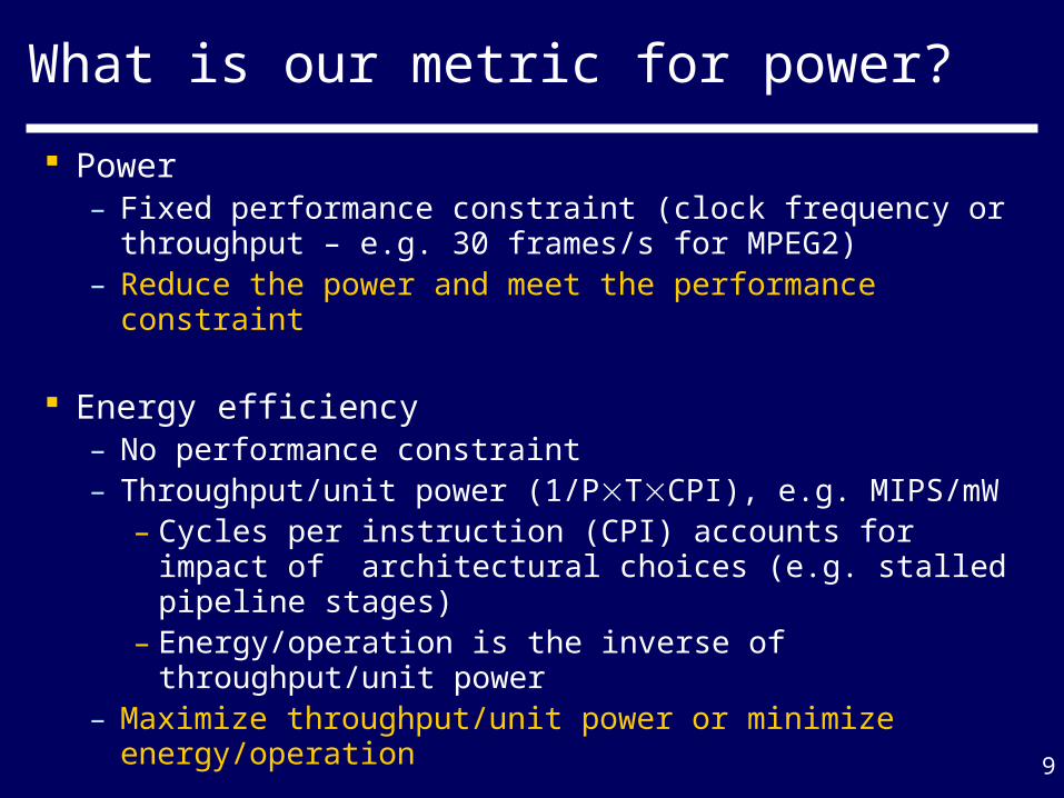
What is our metric for power?
Power– Fixed performance constraint (clock frequency or
throughput – e.g. 30 frames/s for MPEG2)– Reduce the power and meet the performance
constraint
Energy efficiency – No performance constraint– Throughput/unit power (1/PTCPI), e.g. MIPS/mW
– Cycles per instruction (CPI) accounts for impact of architectural choices (e.g. stalled pipeline stages)
– Energy/operation is the inverse of throughput/unit power
– Maximize throughput/unit power or minimize energy/operation

10
What is the power gap? ARM cores
×2 to ×3 gap between custom and hard macro ARMs
×1.3 to ×1.4 gap between ARM7TDMI-S and ARM7TDMI
×3 to ×4 overall from synthesizable to custom ARMs
Comparison of Custom and Hard Macro ARM Implementations
0.0
1.0
2.0
3.0
0.60 0.50 0.35 0.25 0.18 0.13Process Technology (um)
Dh
rys
ton
e 2
.1 M
IPS
/mW
Burd
StrongARM
XScale
TechnologySynthesizable ARM7TDMI-S
Hard Macro ARM7TDMI ratio
0.25 um 0.83 1.17 1.40.18 um 2.28 3.00 1.30.13 um 8.33 11.06 1.3
Core MIPS/mW (excludes cache, etc.)
11
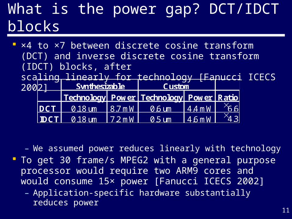
What is the power gap? DCT/IDCT blocks ×4 to ×7 between discrete cosine transform (DCT)
and inverse discrete cosine transform (IDCT) blocks, after scaling linearly for technology [Fanucci ICECS 2002]
– We assumed power reduces linearly with technology To get 30 frame/s MPEG2 with a general purpose
processor would require two ARM9 cores and would consume 15× power [Fanucci ICECS 2002]– Application-specific hardware substantially reduces
power
Technology Power Technology Power RatioDCT 0.18 um 8.7 mW 0.6 um 4.4 mW 6.6IDCT 0.18 um 7.2 mW 0.5 um 4.6 mW 4.3
Synthesizable Custom

12
Outline
Motivation for focusing on reducing ASIC power The power gap between ASIC and custom Where does the power go? What can we do about it? Conclusions on automating low power techniques

13
Breakdown of power by functionality
Typical breakdown of on-chip power consumption for an embedded microprocessor Clock 20% to 40% Memory 20% to 40% Control + datapath 40% to 60% Input/output to off-chip ~5%
Most of power is in datapath, control, clock tree and memory – Techniques focus on reducing this power– Several companies provide custom memory for ASIC
processes, so we won’t discuss memory here

14
Summary of factors effect on active powerAutomated designs are higher power than custom because of …
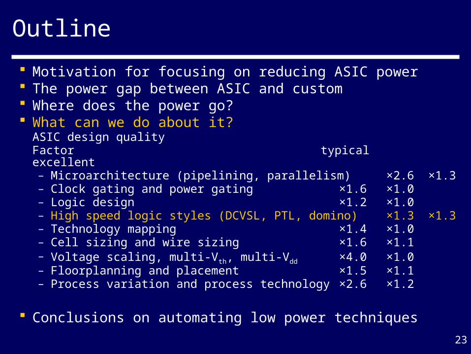
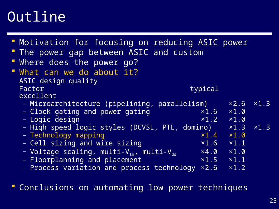
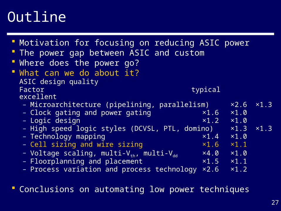
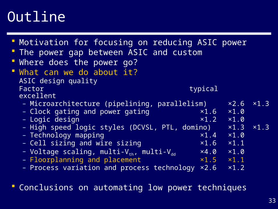
ASIC design qualityFactor typical excellent Microarchitecture (pipelining, parallelism) ×2.6 ×1.3 Clock gating and power gating ×1.6 ×1.0 Logic design ×1.2 ×1.0 High speed logic styles (DCVSL, PTL, domino) ×1.3 ×1.3 Technology mapping ×1.4 ×1.0 Cell sizing and wire sizing ×1.6 ×1.1 Voltage scaling, multi-Vth, multi-Vdd ×4.0 ×1.0 Floorplanning and placement ×1.5 ×1.1 Process variation and process technology ×2.6 ×1.2

15
Outline
Motivation for focusing on reducing ASIC power The power gap between ASIC and custom Where does the power go? What can we do about it? Conclusions on automating low power techniques

16
Outline
Motivation for focusing on reducing ASIC power The power gap between ASIC and custom Where does the power go? What can we do about it?
ASIC design qualityFactor typical excellent– Microarchitecture (pipelining, parallelism) ×2.6 ×1.3– Clock gating and power gating ×1.6 ×1.0– Logic design ×1.2 ×1.0– High speed logic styles (DCVSL, PTL, domino) ×1.3 ×1.3– Technology mapping ×1.4 ×1.0– Cell sizing and wire sizing ×1.6 ×1.1– Voltage scaling, multi-Vth, multi-Vdd ×4.0 ×1.0– Floorplanning and placement ×1.5 ×1.1– Process variation and process technology ×2.6 ×1.2
Conclusions on automating low power techniques

17
Microarchitecture
Increase throughput/cycle to allow Vdd reduction Pipelining inserts registers,
increasing throughput Limited by
– Reduction in instructions/cycle (1/CPI) due to branch misprediction, waiting to read or write memory, etc.
– Power and delay for registers, data forwarding logic, and branch prediction
Parallelism increases throughputin exchange for increased area
Limited by– Routing, multiplexing, control
overheads
leverage for voltage scaling and sizing
instruction fetch
memory access
instruction decode
write back
ALU
instruction fetch
memory access
instruction decode
write back
ALUinsert
registers

18
Microarchitecture: pipelining model
Pipeline power model [Harstein 2003]:– n stages, =1.1 latch growth vs. n, =0.05 for register power
Minimum stage delay: – ASIC tpipelining overhead of 10 FO4 (register delay) + 10 FO4 (imbalance)– Custom tpipelining overhead of 2.6 FO4 total, same tcombinational of 175 FO4
CPI penalty 0.025/stage for custom, and 0.05/stage for ASICs Add fits for dynamic and leakage power with voltage scaling and sizing At 40 FO4 delay constraint (500MHz for Leff=0.1um), ASIC is 2.6 worse
leverage for voltage scaling and sizing
ASICcustom 0.050 vs. 0.019 => ×2.6
1/(e
ner
gy/o
per
atio
n)
stages nslack used for
size, vdd, vth slack used for
size, vdd, vthstages n
1/(e
ner
gy/o
per
atio
n)

19
Microarchitecture
Custom IDCT – pipelining to reduce Vdd [Xanthapoulos JSSC’99] With pipeline: Vdd=1.32V, 20% power overhead Without pipeline: Vdd=2.2V to meet throughput
Parallel datapaths [Bhavnagarwala IEEE Trans. VLSI’00] 2 to 4 reduction in power by reducing Vdd by
increasing throughput with parallel datapaths
Microarchitecture speed gap is 1.8 (typical) to 1.3 (excellent) At a tight delay constraint, this corresponds to about
2.6 to 1.3 worse power due to higher Vdd, lower Vth, and wider gates to compensate
leverage for voltage scaling and sizing
2

20
Outline
Motivation for focusing on reducing ASIC power The power gap between ASIC and custom Where does the power go? What can we do about it?
ASIC design qualityFactor typical excellent– Microarchitecture (pipelining, parallelism) ×2.6 ×1.3– Clock gating and power gating ×1.6 ×1.0– Logic design ×1.2 ×1.0– High speed logic styles (DCVSL, PTL, domino) ×1.3 ×1.3– Technology mapping ×1.4 ×1.0– Cell sizing and wire sizing ×1.6 ×1.1– Voltage scaling, multi-Vth, multi-Vdd ×4.0 ×1.0– Floorplanning and placement ×1.5 ×1.1– Process variation and process technology ×2.6 ×1.2
Conclusions on automating low power techniques
21
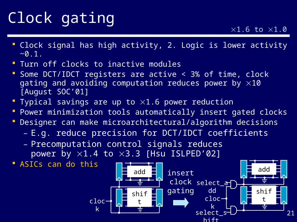
Clock gating
Clock signal has high activity, 2. Logic is lower activity ~0.1. Turn off clocks to inactive modules Some DCT/IDCT registers are active < 3% of time, clock
gating and avoiding computation reduces power by 10 [August SOC’01]
Typical savings are up to 1.6 power reduction Power minimization tools automatically insert gated clocks Designer can make microarchitectural/algorithm decisions
– E.g. reduce precision for DCT/IDCT coefficients– Precomputation control signals reduces
power by 1.4 to 3.3 [Hsu ISLPED’02] ASICs can do this add
clock
select_shift
select_add
shift
1.6 to 1.0
add
clock shift
insertclock gating

22
Power gating
Turn off leakage path in inactive modules– May need to preserve the state registers
Can reduce standby leakage by 3 orders of magnitude[Mutoh JSSC’95]
Other approaches – reverse biasing the substrate– setting input vectors to low leakage states, gives 1.4
leakage reduction [Lee DAC’03] Just now getting ASIC methodology support
– Need large sleep transistors to turn off power– Sleep transistors reduce available supply voltage
reduces leakage in standby
add
clock
select_shift
select_add
shift
23
Outline
Motivation for focusing on reducing ASIC power The power gap between ASIC and custom Where does the power go? What can we do about it?
ASIC design qualityFactor typical excellent– Microarchitecture (pipelining, parallelism) ×2.6 ×1.3– Clock gating and power gating ×1.6 ×1.0– Logic design ×1.2 ×1.0– High speed logic styles (DCVSL, PTL, domino) ×1.3 ×1.3– Technology mapping ×1.4 ×1.0– Cell sizing and wire sizing ×1.6 ×1.1– Voltage scaling, multi-Vth, multi-Vdd ×4.0 ×1.0– Floorplanning and placement ×1.5 ×1.1– Process variation and process technology ×2.6 ×1.2
Conclusions on automating low power techniques

24
High speed logic styles
Low power designs use mostly static CMOS logic Static CMOS logic is low leakage, robust PMOS pullup series transistors are slow
Faster custom logic styles speedup critical paths Custom can use slack from higher speed
(1.4) to reduce power by lowering Vdd
– ASIC power 1.3 worse than custom at a tight delay constraint due to logic style
leverage for voltage scaling and sizing
static CMOS
slow, larger capacitance
PMOS transistorsin series DCVSL dominoPTL
25% lower
domino
22% higher
Delay
Pow
er
32-bit Adder [Tiwari DAC’98]
static
25
Outline
Motivation for focusing on reducing ASIC power The power gap between ASIC and custom Where does the power go? What can we do about it?
ASIC design qualityFactor typical excellent– Microarchitecture (pipelining, parallelism) ×2.6 ×1.3– Clock gating and power gating ×1.6 ×1.0– Logic design ×1.2 ×1.0– High speed logic styles (DCVSL, PTL, domino) ×1.3 ×1.3– Technology mapping ×1.4 ×1.0– Cell sizing and wire sizing ×1.6 ×1.1– Voltage scaling, multi-Vth, multi-Vdd ×4.0 ×1.0– Floorplanning and placement ×1.5 ×1.1– Process variation and process technology ×2.6 ×1.2
Conclusions on automating low power techniques
26
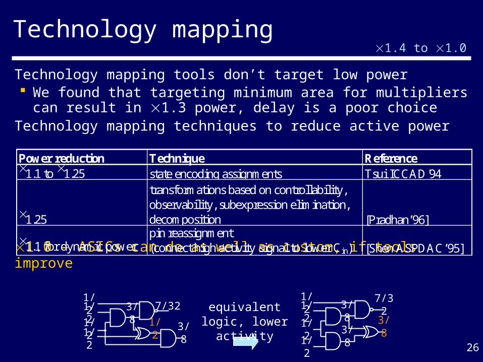
Technology mapping
Technology mapping tools don’t target low power We found that targeting minimum area for multipliers
can result in 1.3 power, delay is a poor choiceTechnology mapping techniques to reduce active power
1.0 – ASICs can do as well as custom, if tools improve
1.4 to 1.0
3/8
3/87/321/2
1/2
1/2
1/2
3/8
1/2 7/321/2
1/21/2 3/81/2
3/8
Power reduction Technique Reference1.1 to 1.25 state encoding assignments Tsui ICCAD'94
1.25
transformations based on controllability, observability, subexpression elimination, decomposition [Pradhan’96]
1.1 for dynamic powerpin reassignment (connect high activity signal to lower Cin) [Shen ASPDAC’95]
equivalent logic, lower activity
27
Outline
Motivation for focusing on reducing ASIC power The power gap between ASIC and custom Where does the power go? What can we do about it?
ASIC design qualityFactor typical excellent– Microarchitecture (pipelining, parallelism) ×2.6 ×1.3– Clock gating and power gating ×1.6 ×1.0– Logic design ×1.2 ×1.0– High speed logic styles (DCVSL, PTL, domino) ×1.3 ×1.3– Technology mapping ×1.4 ×1.0– Cell sizing and wire sizing ×1.6 ×1.1– Voltage scaling, multi-Vth, multi-Vdd ×4.0 ×1.0– Floorplanning and placement ×1.5 ×1.1– Process variation and process technology ×2.6 ×1.2
Conclusions on automating low power techniques

28
Cell sizing and wire sizing
1.35 power reduction on Xtensa processor at 325MHz by (mostly sizing) power minimization with Design Compiler and 0.13um library [internship at Tensilica]
Can do better than Design Compiler (DC) with cell sizing via linear program (LP) (global optimization vs. greedy “pin-hole” optimization), about 1.1 to 1.2 power reduction
1.6 to 1.1
ISCAS'85 # logic Minimum
Netlist levels # cells Delay (ns) DC LP DC LP
c17 4 10 0.094 1.11 1.08 0.86 0.76c432 24 259 0.733 2.78 2.25 2.22 1.76c499 25 644 0.701 5.83 4.62 4.98 3.76c880 23 484 0.700 3.37 3.49 2.83 2.61
c1355 27 764 0.778 6.88 5.53 5.97 4.12c1908 33 635 0.999 3.26 3.11 2.67 2.44c2670 23 1164 0.649 9.23 8.63 8.08 6.90c3540 36 1283 1.054 6.69 5.79 5.60 4.70c5315 34 1956 0.946 10.39 9.51 8.82 7.81c6288 113 3544 3.305 6.91 6.07 6.08 4.78c7552 31 2779 0.847 18.02 16.65 15.60 13.63
Average savings vs. Design Compiler: 10% 16%
Power (mW)
1.1Tmin 1.2Tmin
[Chinnery, Keutzer will be at ISLPED’05]

29
Cell sizing and wire sizing
Cell libraries lack fine-grained sizes and skewed P:N drives
– [Hurat SNUG’01] Generate new cells: 1.2 power reduction and 1.15 faster for bus controller, 1.4 MHz/mW
Simultaneous buffer and wire sizing reduced clock tree power by 2.7 [Gong ISLPED’96]– 1.1 to 1.2 reduction in total power– Not available for ASIC interconnect yet
Up to 1.6 gap due to cell sizing and wire sizing, can reduce to 1.1 using a library with finely-grained sizes, a good sizing tool, and design-specific cells
1.6 to 1.1
Vdd
GND
optimizetransistor
sizes
Vdd
GND

30
Outline
Motivation for focusing on reducing ASIC power The power gap between ASIC and custom Where does the power go? What can we do about it?
ASIC design qualityFactor typical excellent– Microarchitecture (pipelining, parallelism) ×2.6 ×1.3– Clock gating and power gating ×1.6 ×1.0– Logic design ×1.2 ×1.0– High speed logic styles (DCVSL, PTL, domino) ×1.3 ×1.3– Technology mapping ×1.4 ×1.0– Cell sizing and wire sizing ×1.6 ×1.1– Voltage scaling, multi-Vth, multi-Vdd ×4.0 ×1.0– Floorplanning and placement ×1.5 ×1.1– Process variation and process technology ×2.6 ×1.2
Conclusions on automating low power techniques

31
Dynamic supply and substrate biasing Change Vdd based on processor load
– 10 more energy efficient at low performance [Burd ISSCC’00]
– Adaptive voltage scaling with the ARM11 gives 1.7 power reduction for voice, SMS, web applications [National Semiconductor, ARM ’02]
Reduce Vdd and bias substrate to lower Vth
– 1.7 reduction in power, same speed [Hamada CICC’98]
– Increase Vth in standby to reduce leakage
These are complicated to automate for ASICs – Dynamic voltage requires accurate knowledge of path
delays
4.0 to 1.0
[Burd ISSCC 2000]
Energy (mW/MIPS)
MIP
S

32
Multiple supply and threshold voltagesBasic idea: high speed where critical, low power elsewhere Dual Vdd reduces power by 1.7 after substrate
biasing/lower Vdd [Usami JSSC’98]– 2 reduction in clock tree power by using low Vdd
Separate voltage islands – different speeds and Vdd [Lackey ICCAD’02]– Turn off Vdd to modules not in use, reduces leakage by 500– 1.25 to 3 average power reduction, depending on activities
Dual Vth can give 3 to 6 reduction in leakage[Sirichotiyakul DAC’99]
ASICs are limited to Vdd and Vth offered by library and foundry Can’t change Vth to design-specific optimal point Standard cell libraries characterized at only two or three Vdd
Dual Vdd requires level converters and dual Vdd layout
4.0 to 1.0
33
Outline
Motivation for focusing on reducing ASIC power The power gap between ASIC and custom Where does the power go? What can we do about it?
ASIC design qualityFactor typical excellent– Microarchitecture (pipelining, parallelism) ×2.6 ×1.3– Clock gating and power gating ×1.6 ×1.0– Logic design ×1.2 ×1.0– High speed logic styles (DCVSL, PTL, domino) ×1.3 ×1.3– Technology mapping ×1.4 ×1.0– Cell sizing and wire sizing ×1.6 ×1.1– Voltage scaling, multi-Vth, multi-Vdd ×4.0 ×1.0– Floorplanning and placement ×1.5 ×1.1– Process variation and process technology ×2.6 ×1.2
Conclusions on automating low power techniques

34
Floorplanning and placement
Poor floorplanning and cell placement, inaccurate wire loads ×1.5 worse power than custom
We compared partitioning a design into 50K vs. 200K gate modules from 0.25um to 0.13um 42% longer wires for 200K partitions Interconnect is 20% to 40% of total power
[Sylvester ICCAD’98] 1.1 to 1.2 increase in total power due to
wiring, and gates will be upsized to drive the longer wires
1.5 to 1.1
[Hauck Micro.
Report ’01]
automatic place and
route
blockpartitioned
35
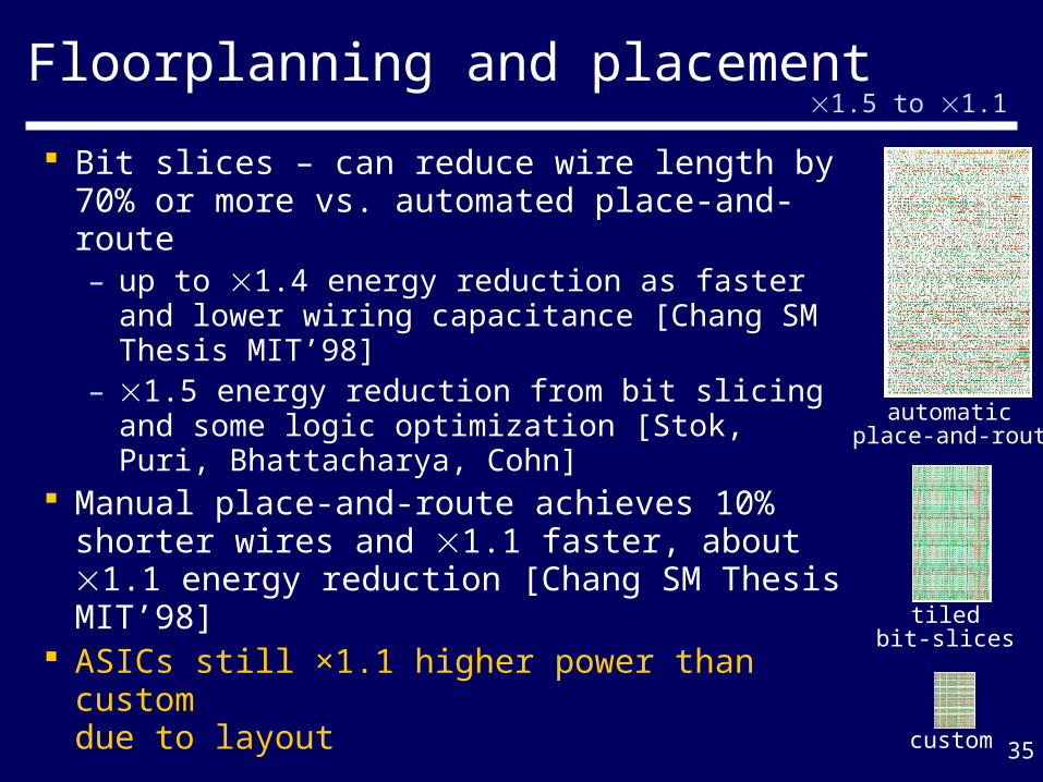
Floorplanning and placement
Bit slices – can reduce wire length by 70% or more vs. automated place-and-route– up to 1.4 energy reduction as faster and
lower wiring capacitance [Chang SM Thesis MIT’98]
– 1.5 energy reduction from bit slicing and some logic optimization [Stok, Puri, Bhattacharya, Cohn]
Manual place-and-route achieves 10% shorter wires and 1.1 faster, about 1.1 energy reduction [Chang SM Thesis MIT’98]
ASICs still ×1.1 higher power than custom due to layout
1.5 to 1.1
automatic place-and-route
tiled bit-slices
custom

36
Outline
Motivation for focusing on reducing ASIC power The power gap between ASIC and custom Where does the power go? What can we do about it?
ASIC design qualityFactor typical excellent– Microarchitecture (pipelining, parallelism) ×2.6 ×1.3– Clock gating and power gating ×1.6 ×1.0– Logic design ×1.2 ×1.0– High speed logic styles (DCVSL, PTL, domino) ×1.3 ×1.3– Technology mapping ×1.4 ×1.0– Cell sizing and wire sizing ×1.6 ×1.1– Voltage scaling, multi-Vth, multi-Vdd ×4.0 ×1.0– Floorplanning and placement ×1.5 ×1.1– Process variation and process technology ×2.6 ×1.2
Conclusions on automating low power techniques
37
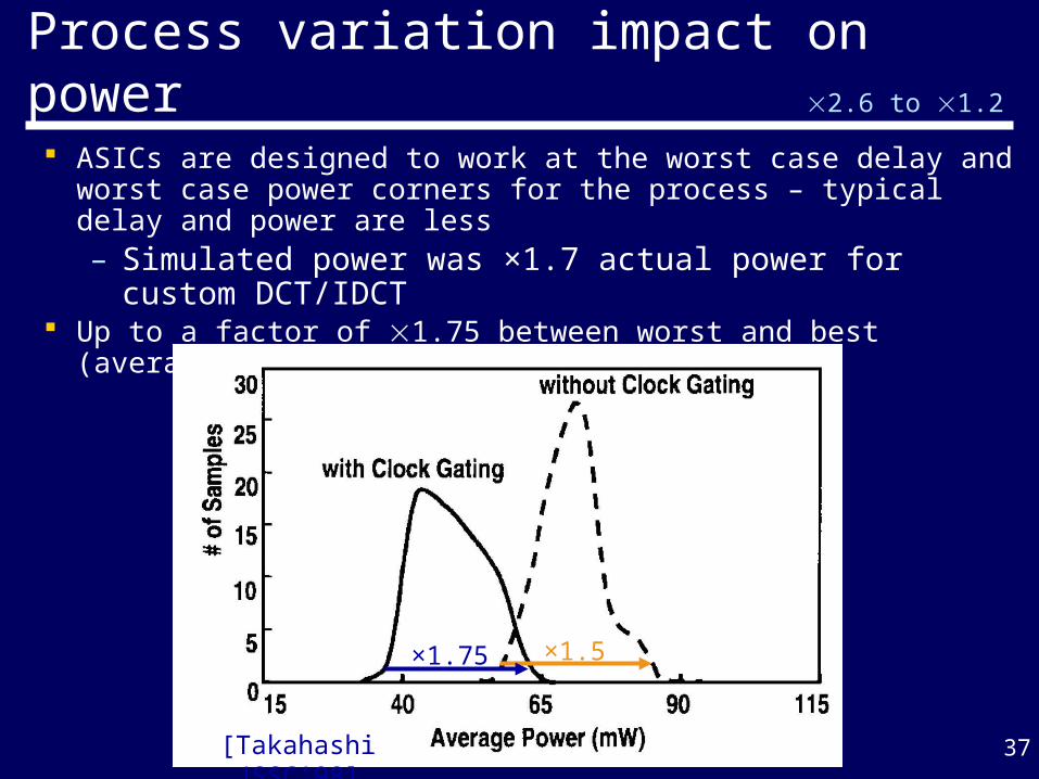
Process variation impact on power
ASICs are designed to work at the worst case delay and worst case power corners for the process – typical delay and power are less– Simulated power was ×1.7 actual power for custom
DCT/IDCT Up to a factor of 1.75 between worst and best (average power
of 80 chip samples in 0.3um)
2.6 to 1.2
×1.75 ×1.5
[Takahashi JSSC’98]
38
×1.4low
power bin higher
power bin
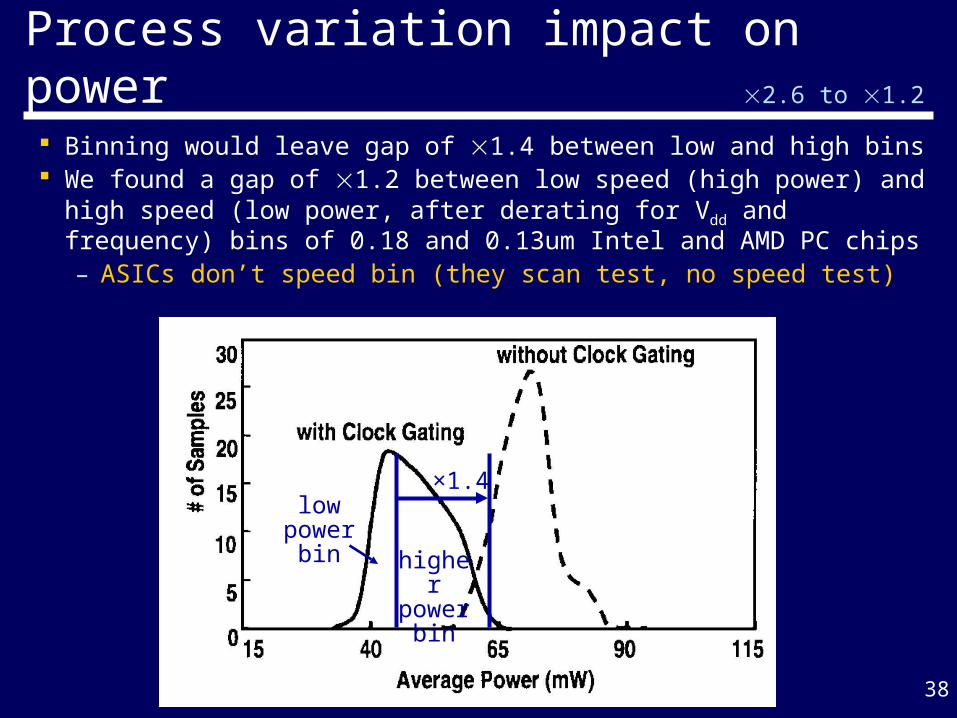
Process variation impact on power
Binning would leave gap of 1.4 between low and high bins We found a gap of 1.2 between low speed (high power)
and high speed (low power, after derating for Vdd and frequency) bins of 0.18 and 0.13um Intel and AMD PC chips – ASICs don’t speed bin (they scan test, no speed test)
2.6 to 1.2

39
Process technology
Low power libraries are more expensive– 5% to 10% transistor width shrinks to reduce capacitances– Copper is 40% lower resistivity than aluminum– Low-k dielectric reduces wire capacitances – we estimate
about a ×1.1 reduction in total power with a low-k dielectric – Silicon-on-insulator is ×1.1 to ×1.3 faster, ×1.4 power
reduction [Narendra Symp. VLSI 2001]
We compared cell libraries in UMC 0.13um vs. IBM 0.13um process – IBM cells about ×1.05 faster, ×1.6 higher active power,
UMC had ×17 leakage
Overall impact of process variation and technology 2.6 ASIC power relative to custom for worst case conditions
and a cheap process 1.2 in a low power process, typical conditions, no speed
binning
2.6 to 1.2

40
Outline
Motivation for focusing on reducing ASIC power The power gap between ASIC and custom Where does the power go? What can we do about it? Conclusions on automating low power techniques

41
Low power design conclusions
Typical ASIC is 3 to 7 less energy efficient than custom– We assumed ASIC and custom designs can use the
same microarchitectural and logic design techniques. These are the biggest levers for reducing power.
– Can get 10 or more going from general purpose hardware to application-specific hardware. – E.g. Fast Fourier transform implementations as
discussed in Andrew Chang’s paper. The largest factor for the power gap is voltage
scaling – responsible for up to ×4
Process and microarchitecture can be large factors, about ×2.6 each

42
Low power design conclusions
By incorporating custom techniques can get within
3 at a high performance target– Can’t use custom logic styles– ASIC speed penalty drags down efficiency, as
higher Vdd, lower Vth, and upsized gates are needed to meet performance target
1.5 at a lower performance target (~2 slower)– Make full use of scaling down Vdd and Vth
43
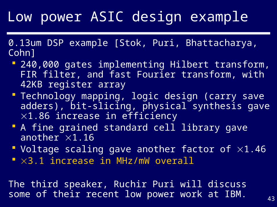
Low power ASIC design example
0.13um DSP example [Stok, Puri, Bhattacharya, Cohn] 240,000 gates implementing Hilbert transform, FIR
filter, and fast Fourier transform, with 42KB register array
Technology mapping, logic design (carry save adders), bit-slicing, physical synthesis gave 1.86 increase in efficiency
A fine grained standard cell library gave another 1.16
Voltage scaling gave another factor of 1.46 3.1 increase in MHz/mW overall
The third speaker, Ruchir Puri will discuss some of their recent low power work at IBM.

Extra slides

45
Impact of voltage scaling on power
Ptotal = Pdynamic + Pshort circuit + Pstatic
Short circuit power when switching is 10% or less of Ptotal
Dynamic power due to switching of capacitances
– Reducing Vdd gives quadratic reduction in Pdynamic But transistor drive current depends on Vdd
– Must reduce Vth to maintain drive current But reducing Vth increases subthreshold leakage
current, which is the major contributor to Pstatic
(Clock frequency f; gate switching activity ; capacitance C; transistor length L; transistor gate oxide thickness Tox; temperature T; constants , , Io, and m.)
Vdd
Cload
Vth,p
Vth,n
Vdd
Vth,p
Vth,n
short circuit current
Vdd
VddVth,n
Vth,p
Vdd
0VVth,n
Vth,psubthreshold
leakage
[Chen in Trans. On Electron Devices 1997]
dynamic power

46
0.001
0.01
0.1
1
10
100
1000
0.13 0.09 0.065 0.045 0.022Technology (um)
Pow
er/D
ie A
rea
(W/c
m2 )
high speed, total powerhigh speed, leakagelow power, total powerlow power, leakage
ITRS leakage power trends
From International Technology Roadmap for Semiconductors data for 2001-2016 (assuming activity of 0.1, ignoring interconnect).
fast, low Vth slow, high Vth
leakage increasing
Can’t scale down Vth much further due to large subthreshold leakage currents
Gate tunneling leakage through thin gate oxide Tox is also becoming a significant cause of leakage
Further Vdd voltage scaling will be limited
Must also look to other low power techniques

47
Summary of factors affecting (active) power
Automated designs are higher power than custom because of …
ASIC design qualityFactor typical excellent Microarchitecture (pipelining, parallelism) ×2.6 ×1.3 Memory ×1.4 ×1.0 Clock gating and power gating ×1.6 ×1.0 Logic design ×1.2 ×1.0 High speed logic styles (DCVSL, PTL, domino) ×1.3 ×1.3 Technology mapping ×1.4 ×1.0 Cell sizing and wire sizing ×1.6 ×1.1 Voltage scaling, multi-Vth, multi-Vdd ×4.0 ×1.0 Floorplanning and placement ×1.5 ×1.1 Process variation and process technology ×2.6 ×1.2

48
Memory – reduce cache misses Larger caches consume more power, but reduced cache misses
– Pipeline stalls, waits many cycles for read/write to off-chip memory
Caches with higher associativity (e.g. 8-way vs. direct mapped) consume more power, also affects likelihood of a cache miss
[Duarte ASIC/SOC 2001]– Sub-banking: only precharge the need section
of the cache bank, 1.32 energy savings– Software optimizations to reduce cache misses
gave on average a 1.6 reduction in power 90% of the StrongARM area was caches, increasing
the transistor length in the caches by 12% reduced leakage by 20 [Montanaro JSSC’96]
ASICs can do this, custom memory is available for ASICs
on-chip cache
slower off-chip memory
write buffer
processor
1.4 to 1.0

49
Outline
Motivation for focusing on reducing ASIC power The power gap between ASIC and custom Where does the power go? What can we do about it?
ASIC design qualityFactor typical excellent– Microarchitecture (pipelining, parallelism) ×2.6 ×1.3– Clock gating and power gating ×1.6 ×1.0– Logic design ×1.2 ×1.0– High speed logic styles (DCVSL, PTL, domino) ×1.3 ×1.3– Technology mapping ×1.4 ×1.0– Cell sizing and wire sizing ×1.6 ×1.1– Voltage scaling, multi-Vth, multi-Vdd ×4.0 ×1.0– Floorplanning and placement ×1.5 ×1.1– Process variation and process technology ×2.6 ×1.2
Conclusions on automating low power techniques
50
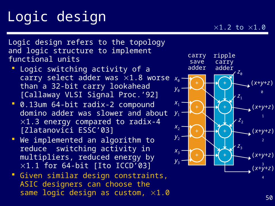
Logic design
Logic design refers to the topology and logic structure to implement functional units Logic switching activity of a carry
select adder was 1.8 worse than a 32-bit carry lookahead [Callaway VLSI Signal Proc.’92]
0.13um 64-bit radix-2 compound domino adder was slower and about 1.3 energy compared to radix-4 [Zlatanovici ESSC’03]
We implemented an algorithm to reduce switching activity in multipliers, reduced energy by 1.1 for 64-bit [Ito ICCD’03]
Given similar design constraints, ASIC designers can choose the same logic design as custom, 1.0
1.2 to 1.0
+
+
+
+ +
+
+
+x0
x1
x2
x3
y0
y1
y2
y3
z0
z2
z1
z3
(x+y+z)1
(x+y+z)0
(x+y+z)2
(x+y+z)3
(x+y+z)4
carry save adder
ripple carry adder