Embed Size (px)
Citation preview
8/6/2019 Clint Inverter Paper
http://slidepdf.com/reader/full/clint-inverter-paper 1/13
Abstract — Inverters are used in a large number of powerapplications. The function of an inverter is to convert DC
power to AC, these are referred to as Voltage SourceInverters (VSI). VSI are divided up into three categories:Pulse-width Modulated Inverters, Square-wave Inverters,
and Single-phase Inverters with Voltage Cancellation. Thispaper will talk about the different types of Inverters and how
they work. It will continue on with examples of some typesof inverters and what types of factors affect their efficiencies.
I. I NTRODUCTION
Within the last decade, there have been major advancements in power electronics. Power electronicshave moved along with these developments with suchthings as digital signal processors being used to control
power systems. An Inverter is basically a converter thatconverts DC-AC power. Inverter circuits can be verycomplex so the objective of this paper is to present someof the inner workings of inverters without getting lost insome of the fine details. A voltage source inverter (VSI)is one that takes in a fixed voltage from a device, such as adc power supply, and converts it to a variable-frequencyAC supply.
Voltage-source inverters are divided into threegeneral categories: Pulse-width Modulated (PWM)Inverters, Square-wave Inverters, Single-phase Inverterswith Voltage Cancellation. Pulse-width modulationinverters take in a constant dc voltage. Diode-rectifiersare used to rectify the line voltage, and the inverter must
control the magnitude and the frequency of the ac outputvoltages. To do this the inverter uses pulse-widthmodulation using it’s switches. There are differentmethods for doing the pulse-width modulation in aninverter in order to shape the output ac voltages to be veryclose to a sine wave. These different methods will bediscussed further with a focus on sinusoidal-PWM.Squire-wave inverters have their input connected to acontrolled dc voltage in order to control the magnitude of the output ac voltage. The inverter only controls thefrequency of the output where the input voltage iscontrolled the magnitude. The output ac voltage has awaveform similar to a square wave which is where theinverter got it’s name. Lastly, Single-phase inverters with
voltage cancellation, take in a constant dc source andoutput a square-wave like ac voltage. They can control both the frequency and the magnitude of the output but donot use PWM and therefore have a square-wave likeoutput. These inverters have combined characteristics of the previous two inverters. The voltage cancellation onlyworks with single phase inverters, not three phase, thiswill be explained more further later on in the paper.
Switch-mode dc-to-ac inverters are used in ac-motor drives and uninterruptible ac power supplies where the
main objective is to provide a sinusoidal ac output wheremagnitude and frequency can both be controlled.
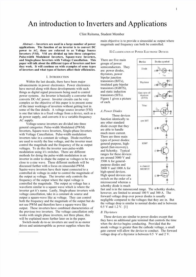
II.CLASSIFICATION OF POWER ELECTRONIC DEVICES
There are five maingroups of power semiconductors. Theyare: power diodes,thyristors, power bipolar junctiontransistors (BJTs),insulated gate bipolar transistors (IGBTS),and static inductiontransistors (SITs).Figure 1 gives a pictureof each.
A. Power Diodes
These devicesfunction identically toany other standarddiode except that theyare able to handlemuch more current.There are three maintypes of power diodes:general-purpose, high-speed (fast-recovery),and Schottky. Typicalranges for these devicesare around 3000 V and3500 A for general- purpose diodes and3000 V and 1000 A for high-speed devices.High speed devices canswitch on the order of amicrosecond whereas aschottky diode is muchfast and is in the nanosecond range. The schottky diodes,however, are limited to around 100 V and 300 A. Theforward voltage drop over power diodes is usuallynegligible compared to the voltages that they are in. Butthe voltage drop is similar to normal diodes and is between0.5 V and 1.2 V. [1]
B. Thyristors
These devices are similar to power diodes except thatthey have an additional gate terminal that controls the timewhen the device begins conducting. Provided that theanode voltage is greater than the cathode voltage, a smallgate current will allow the device to conduct. The forwardvoltage drop of a thyristor is between 0.5 V and 2 V.
An introduction to Inverters and Applications
Clint Reitsma, Student Member
1
8/6/2019 Clint Inverter Paper
http://slidepdf.com/reader/full/clint-inverter-paper 2/13
Once conduction is initiated the gate current has no further control. In order to stop conduction the device must be inreverse-biased; the anode voltage is less than the cathodevoltage. These devices are rated up to 6000 V and 3500A.
The turn-off time of these devices is the time it takes for the device current to go back to zero after putting thedevice in reverse-bias. The fastest turn-off times arearound 10 microseconds. To achieve these turn-off times
devices with lower power ratings must be used. Thyristorsare further classified into the following groups: force-commutated and line-commutated thyristors, gate turn-off thyristors (GTOs), reverse-conducting thyristors (RCTs),static induction thyristors (SITs), gate-assisted turn-off thyristors (GATTs), light-activated silicon controlledrectifiers (LASCRs), and MOS controlled thyristors(MCTs). These devices are all basically a modification of the standard thyristor.
Shown in figure 1 is a triac device. This is basicallytwo thyristors connected back to back to allow control both forwards and backwards. A triac is basically a bidirectional thyristor. The gate turn-off thyristor (GTO),can be turned on by applying a short positive pulse to thegate, like a thyristor, and can also be turned off byapplying a short negative pulse. GTOs are veryconvenient in that they do not need to have other circuitsto control in order to be turned off. [1]
C.Power BJTs
These devices are rated up to 1200V and 400A. Theyoperate very much the same as a normal BJT. Power BJTsare used in power converters such as inverters asfrequencies of up to 10 kHz. Power MOSFETs canoperate at somewhat higher frequencies (a few to severaltens of kHz), but are limited to power ratings, usually1000 V, 50 A. Insulated-gate bipolar transistors (IGBTs)are voltage controlled power transistors that offer better speed than a BJT but are not quite as fast as a power MOSFET. [1]
D.Device History
The earliest switches used to oscillate were mechanicalvibrators. Essentially oscillating mechanical relays, thesedevices were not very efficient or reliable. It was not untilthe 1960s when semi-conductors were being discoveredand the transistor started to make an appearance. Now theSilicon Controlled Rectifier was made that worked aselectronic latching relays. Next the Darlington transistorswere used. These last two devices did prove to be bothreliable and somewhat efficient but still had
disadvantages. When the Metal Oxide Semi-conductingField Effect Transistor (MOSFET) came out, it solved alot of problems. These devices can handle high currentsand have a low resistance. They are easy to connect in acircuit and work well in parallel connections allowing for more current. Some inverters now use the newer IGBTswhich are newer, high power, and low less switchingtransistors.
III. HOW IT WORKS
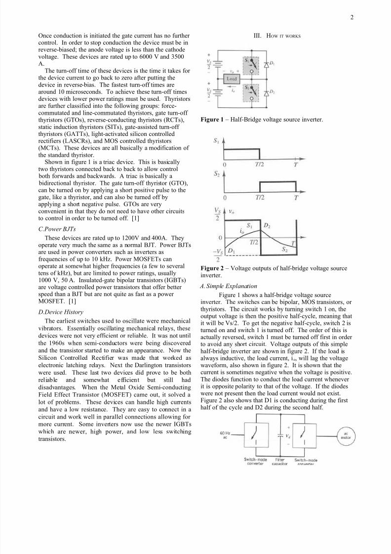
Figure 1 – Half-Bridge voltage source inverter.
Figure 2 – Voltage outputs of half-bridge voltage sourceinverter.
A. Simple Explanation
Figure 1 shows a half-bridge voltage sourceinverter. The switches can be bipolar, MOS transistors, or thyristors. The circuit works by turning switch 1 on, theoutput voltage is then the positive half-cycle, meaning thatit will be Vs/2. To get the negative half-cycle, switch 2 isturned on and switch 1 is turned off. The order of this isactually reversed, switch 1 must be turned off first in order to avoid any short circuit. Voltage outputs of this simplehalf-bridge inverter are shown in figure 2. If the load isalways inductive, the load current, io, will lag the voltagewaveform, also shown in figure 2. It is shown that thecurrent is sometimes negative when the voltage is positive.The diodes function to conduct the load current whenever
it is opposite polarity to that of the voltage. If the diodeswere not present then the load current would not exist.Figure 2 also shows that D1 is conducting during the firsthalf of the cycle and D2 during the second half.
2
8/6/2019 Clint Inverter Paper
http://slidepdf.com/reader/full/clint-inverter-paper 3/13
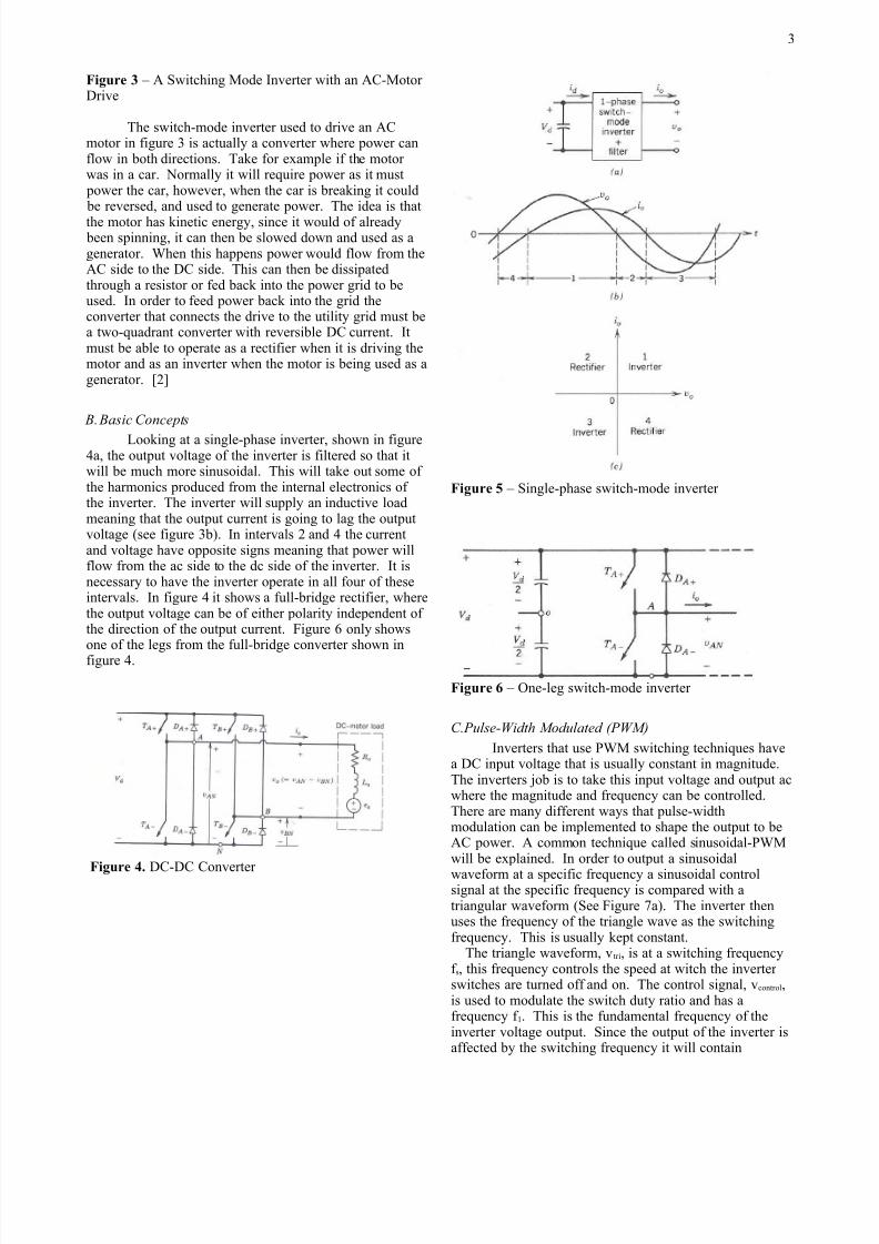
Figure 3 – A Switching Mode Inverter with an AC-Motor Drive
The switch-mode inverter used to drive an ACmotor in figure 3 is actually a converter where power canflow in both directions. Take for example if the motor was in a car. Normally it will require power as it must power the car, however, when the car is breaking it could be reversed, and used to generate power. The idea is that
the motor has kinetic energy, since it would of already been spinning, it can then be slowed down and used as agenerator. When this happens power would flow from theAC side to the DC side. This can then be dissipatedthrough a resistor or fed back into the power grid to beused. In order to feed power back into the grid theconverter that connects the drive to the utility grid must bea two-quadrant converter with reversible DC current. Itmust be able to operate as a rectifier when it is driving themotor and as an inverter when the motor is being used as agenerator. [2]
B.Basic Concepts
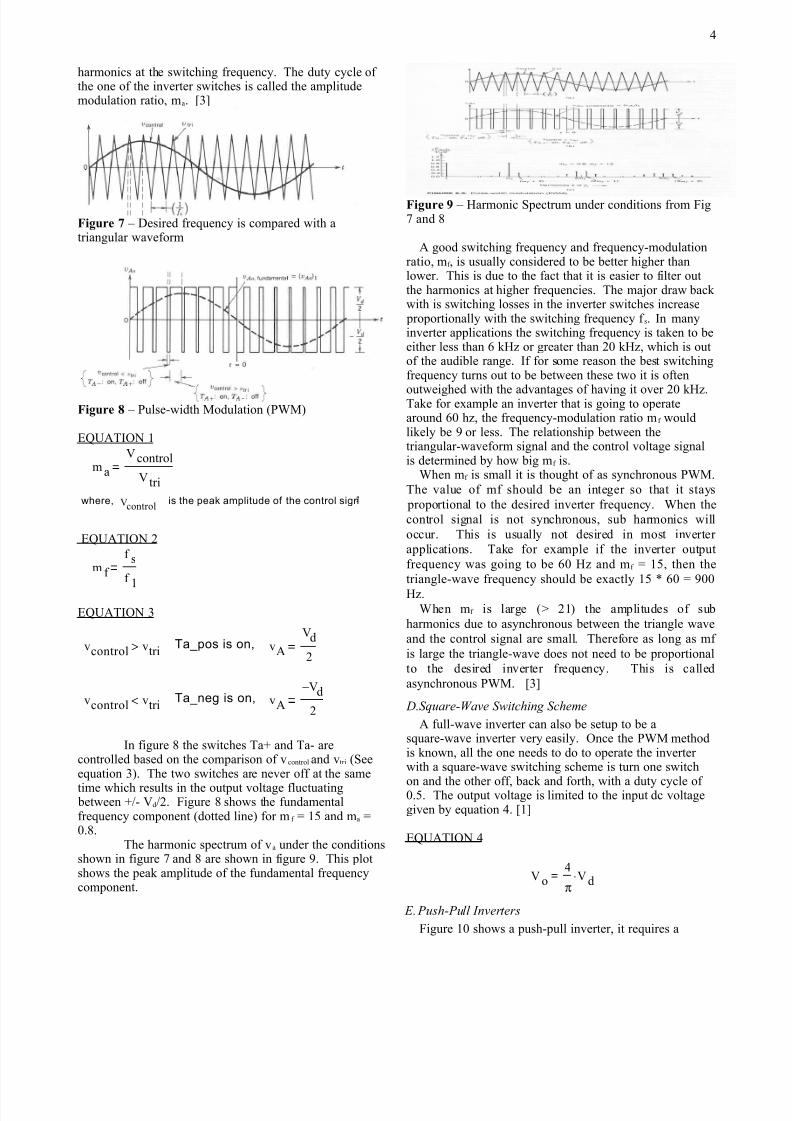
Looking at a single-phase inverter, shown in figure4a, the output voltage of the inverter is filtered so that itwill be much more sinusoidal. This will take out some of the harmonics produced from the internal electronics of the inverter. The inverter will supply an inductive loadmeaning that the output current is going to lag the outputvoltage (see figure 3b). In intervals 2 and 4 the currentand voltage have opposite signs meaning that power willflow from the ac side to the dc side of the inverter. It isnecessary to have the inverter operate in all four of theseintervals. In figure 4 it shows a full-bridge rectifier, wherethe output voltage can be of either polarity independent of the direction of the output current. Figure 6 only showsone of the legs from the full-bridge converter shown infigure 4.
Figure 4. DC-DC Converter
Figure 5 – Single-phase switch-mode inverter
Figure 6 – One-leg switch-mode inverter
C.Pulse-Width Modulated (PWM)
Inverters that use PWM switching techniques havea DC input voltage that is usually constant in magnitude.The inverters job is to take this input voltage and output acwhere the magnitude and frequency can be controlled.There are many different ways that pulse-widthmodulation can be implemented to shape the output to beAC power. A common technique called sinusoidal-PWMwill be explained. In order to output a sinusoidal
waveform at a specific frequency a sinusoidal controlsignal at the specific frequency is compared with atriangular waveform (See Figure 7a). The inverter thenuses the frequency of the triangle wave as the switchingfrequency. This is usually kept constant.
The triangle waveform, vtri, is at a switching frequencyf s, this frequency controls the speed at witch the inverter switches are turned off and on. The control signal, vcontrol,is used to modulate the switch duty ratio and has afrequency f 1. This is the fundamental frequency of theinverter voltage output. Since the output of the inverter isaffected by the switching frequency it will contain
3
8/6/2019 Clint Inverter Paper
http://slidepdf.com/reader/full/clint-inverter-paper 4/13
harmonics at the switching frequency. The duty cycle of the one of the inverter switches is called the amplitudemodulation ratio, ma. [3]
Figure 7 – Desired frequency is compared with atriangular waveform
Figure 8 – Pulse-width Modulation (PWM)
EQUATION 1
m a
V control
V tri
where, Vcontrolis the peak amplitude of the control sign
EQUATION 2
m f
f s
f
1
EQUATION 3
vcontrol vtri> Ta_pos is on, vA
Vd
2
vcontrol vtri< Ta_neg is on, vA
Vd−
2
In figure 8 the switches Ta+ and Ta- arecontrolled based on the comparison of vcontrol and vtri (Seeequation 3). The two switches are never off at the same
time which results in the output voltage fluctuating between +/- Vd/2. Figure 8 shows the fundamentalfrequency component (dotted line) for m f = 15 and ma =0.8.
The harmonic spectrum of va under the conditionsshown in figure 7 and 8 are shown in figure 9. This plotshows the peak amplitude of the fundamental frequencycomponent.
Figure 9 – Harmonic Spectrum under conditions from Fig7 and 8
A good switching frequency and frequency-modulationratio, mf , is usually considered to be better higher thanlower. This is due to the fact that it is easier to filter outthe harmonics at higher frequencies. The major draw back with is switching losses in the inverter switches increase proportionally with the switching frequency f s. In manyinverter applications the switching frequency is taken to beeither less than 6 kHz or greater than 20 kHz, which is outof the audible range. If for some reason the best switchingfrequency turns out to be between these two it is often
outweighed with the advantages of having it over 20 kHz.Take for example an inverter that is going to operatearound 60 hz, the frequency-modulation ratio mf wouldlikely be 9 or less. The relationship between thetriangular-waveform signal and the control voltage signalis determined by how big mf is.
When mf is small it is thought of as synchronous PWM.The value of mf should be an integer so that it stays proportional to the desired inverter frequency. When thecontrol signal is not synchronous, sub harmonics willoccur. This is usually not desired in most inverter applications. Take for example if the inverter outputfrequency was going to be 60 Hz and mf = 15, then thetriangle-wave frequency should be exactly 15 * 60 = 900
Hz.When mf is large (> 21) the amplitudes of sub
harmonics due to asynchronous between the triangle waveand the control signal are small. Therefore as long as mf is large the triangle-wave does not need to be proportionalto the desired inverter frequency. This is calledasynchronous PWM. [3]
D.Square-Wave Switching Scheme
A full-wave inverter can also be setup to be asquare-wave inverter very easily. Once the PWM methodis known, all the one needs to do to operate the inverter with a square-wave switching scheme is turn one switch
on and the other off, back and forth, with a duty cycle of 0.5. The output voltage is limited to the input dc voltagegiven by equation 4. [1]
EQUATION 4
V o4
πV d⋅
E. Push-Pull Inverters
Figure 10 shows a push-pull inverter, it requires a
4
8/6/2019 Clint Inverter Paper
http://slidepdf.com/reader/full/clint-inverter-paper 5/13
center-tap transformer. If we assume the output currentflows continuously then the switch T1 is on and T2 is off. Now, T1 will conduct for a positive value of io, and D1would conduct for a negative value of io. This means thatthe direction of io does not matter then, the output voltageis simply vo=Vd/n. In this equation n is the number of turns on the transformer between the primary-half and thesecondary winding. The other state of the inverter is whenT2 is on and T1 is off, the output voltage is now the same
as before except it is negative. A push-pull inverter can beoperated in either the pulse width modulation switchingscheme or the square-wave switching scheme. Theoutputs are the same as before shown in figure 5.
Figure 10. Push-pull inverter (single phase)
EQUATION 5
Vo ma
Vd
n⋅ mawhere <= to 1.0
Vd
n
Vo<4
π
Vd
n
⋅< wher e ma> 1.0
EQUATION 6
VT 2 Vd⋅
IT io
The above equation 5 and 6 show the push-pull inverter,from figure 10, output voltage. One of the mainadvantages of the push-pull inverter is that it is moreefficient for low-voltage input sources, such as a battery.The reason for this is that the voltage drop across more
than one switch in series would result in a significantreduction in energy efficiency. Also, the control drives for the two switches have a common ground. It is hard toavoid the dc saturation of the transformer in a push-pullinverter. The output current from the secondary current of the transformer is slowly varying current at thefundamental output frequency. This is usually assumed to be a constant during a switching interval. When thetransistors are switched the current shifts from one half tothe other half of the primary winding. This required verygood magnetic coupling between these two half-windingsin order to reduce the energy associated with the leakage
inductance of the two primary windings. The energy willthen be dissipated in the switches or in other circuits usedto dissipate and help the switches. It is important that thecurrent in the windings has a place to go when theswitches are switched.
When the push-pull inverter is used in pulse-width-modulation switching scheme for producing a outputsinusoidal output, the transformer must be designed for thefundamental frequency that the inverter will be running at.
That is, the number of turns will be high compared to atransformer designed to operate at the switching frequencyin a switch-mode dc power supply. This will result in ahigh transformer leakage inductance that is proportional tothe square of the number of turns. These constraints makeit hard to use a push-pull inverter for switchingfrequencies of higher than 1kHz. [2]
IV. THREE PHASE I NVERTERS
Many applications that require an inverter use three- phase power. Two main examples are an ac-motor driveand uninterruptible power supplies. One option for a“three-phase” inverter is to use three separate single phase
inverters but vary their output by 120 degrees. This setupwould require lots of hardware including 12 switches for the three inverters used.Figure 11. Three-phase PWM waveforms
It is much more common to use a setup shown infigure 11. This setup consists of three legs, one for each phase. Each leg is basically setup in the same way as theone-leg inverter described above. In three phase inverters pulse-width modulations is used in the same way as it is
5
8/6/2019 Clint Inverter Paper
http://slidepdf.com/reader/full/clint-inverter-paper 6/13
before except that it much be used with each of the three phases. When generating power to three different phasesone must make sure that each phase is equal, meaning thatit is balanced. To ensure this the same triangle voltagewaveform is compared with three sinusoidal controlvoltages that are 120 degrees out of phase.
The Harmonics in the output are only of concern in theline-to-line voltages. The harmonics in the output of anyone of the legs are identical to the harmonics in Va. Only
the odd harmonics exist as sidebands, centered around mf and its multiples, provided, mf is odd. Only consideringthe harmonic of mf, the phase difference will beequivalent to zero if mf is odd and a multiple of 3. As aconsequence, the harmonic at mf is suppressed in the line-to-line voltage vab. The same argument applies in thesuppression of harmonics at the odd multiples of mf, if mf is chosen to be an odd multiple of 3.
Figure 12. Three-Phase Inverter
Therefore, some of the dominant harmonics in theone-leg inverter can be eliminated from the line-to-linevoltage of a three-phase inverter. PWM considerations aresummarized below:For low values of mf, to eliminate the even harmonics, asynchronized PWM should be used and
mf should be an odd integer. Moreover, mf should be amultiple of 3 to cancel out the most dominant harmonicsin the line-line voltage. Moreover, the slopes of Vcontrol andVtri should be of the opposite polarity at the coincidentzero crossings.During over modulation (ma > 1.0), regardless of the valueof mf, the conditions pertinent to a small mf should beobserved. [1]
V. POWER QUALITY
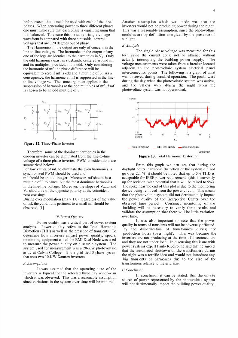
Power quality was a critical part of power systemanalysis. Power quality refers to the Total HarmonicDistortion (THD) as well as the presence of transients. To
determine how inverters impact power quality, specialmonitoring equipment called the BMI Dual Node was usedto measure the power quality on a sample system. Thesystem used for measurement was a 20-KW photovoltaicarray at Calvin College. It is a grid tied 3-phase systemthat uses two 10-KW Xantrex inverters.
A.Assumptions
It was assumed that the operating state of theinverters is typical for the selected three day window inwhich it was observed. This was a reasonable assumptionsince variations in the system over time will be minimal.
Another assumption which was made was that theinverters would not be producing power during the night.This was a reasonable assumption, since the photovoltaicmodules are by definition energized by the presence of sunlight.
B. Analysis
The single phase voltage was measured for thistest, since the current could not be attained without
actually interrupting the building power supply. Thevoltage measurements were taken from a breaker locatedadjacent to the photovoltaic system electrical panelinterconnection points. The following is a graph of whatwas observed during standard operation. The peaks wereduring the day when the photovoltaic system was active,and the valleys were during the night when the photovoltaic system was not operational.
Figure 13. Total Harmonic Distortion
From this graph we can see that during thedaylight hours, harmonic distortion of the system did notgo over 2.1 %, it should be noted that up to 5% THD is
acceptable for IEEE power requirements (this is currentlyup for revision, with potential that it will be raised to 9%).The spike near the end of this plot is due to the monitoringdevice being removed from the power circuit. This meansthat the photovoltaic system did not detrimentally impactthe power quality of the Interpretive Center over theobserved time period. Continued monitoring of the building will be necessary to verify these results andvalidate the assumption that there will be little variationover time.
It was also important to note that the power quality in terms of transients will not be adversely affected by the disconnection of transformers during non production hours (over night). This was because the
inverters are not producing at the time of disconnectionand they are not under load. In discussing this issue with power systems expert Paulo Ribeiro, he said that he agreedthat the automated shutdown of the transformers duringthe night was a terrific idea and would not introduce any big transients or harmonics due to the size of thetransformers relative to the grid size.
C.Conclusion
In conclusion it can be stated, that the on-sitesource of power represented by the photovoltaic systemwill not detrimentally impact the building power quality.
6
8/6/2019 Clint Inverter Paper
http://slidepdf.com/reader/full/clint-inverter-paper 7/13
This was important since the building has a laboratorylocated in it, along with a number of computer workstations which could be adversely affected bysignificant voltage fluctuations.
Inverters by their nature are going to produceharmonics that are not wanted. This must be consideredwhen designing an inverter. Xantrex makes a goodinverter, as shown above, that can be tied into a grid andused without producing unwanted transients and
harmonics.
VI. I NVERTER EXAMPLES
A. Theoretical Analysis - MathCAD
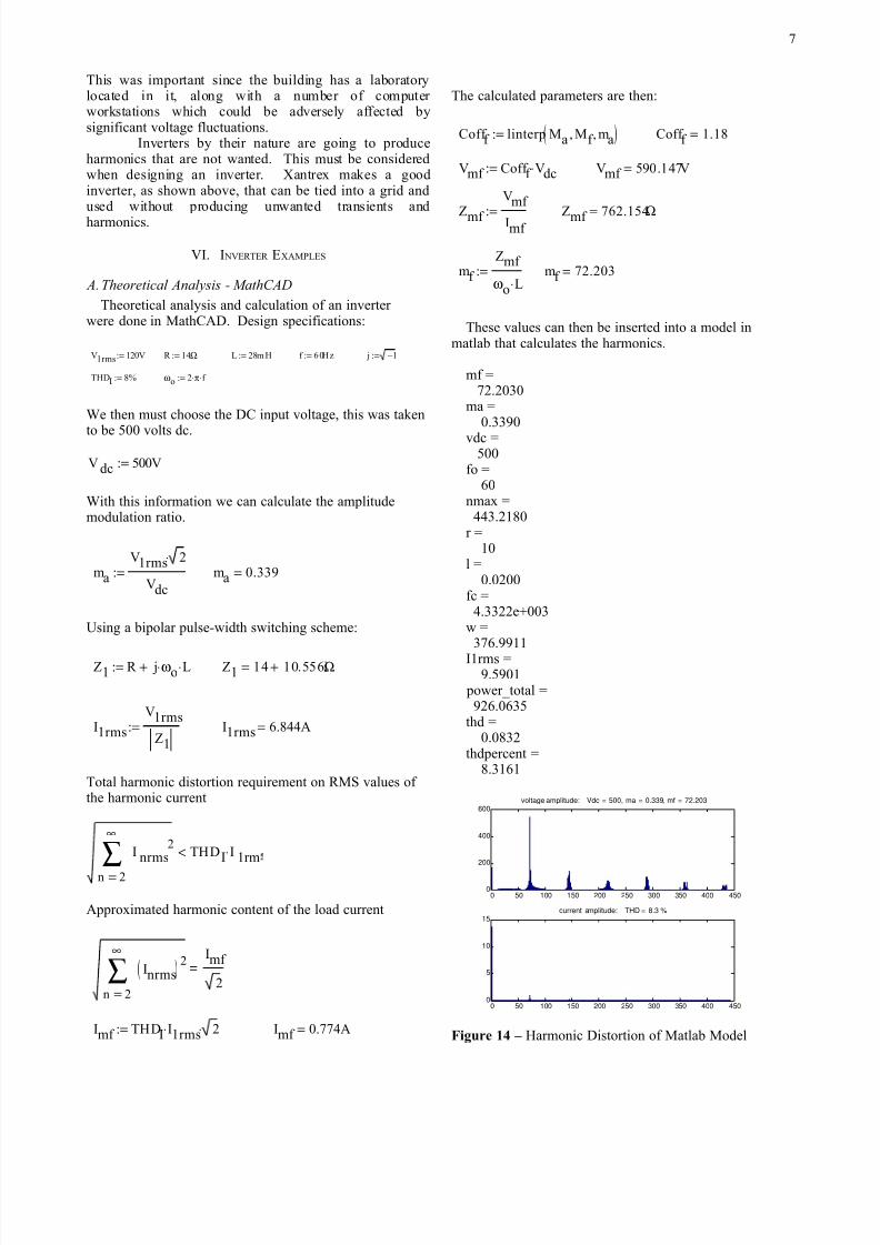
Theoretical analysis and calculation of an inverter were done in MathCAD. Design specifications:
V1rms 120V:= R 14Ω:= L 28m H:= f 6 0H z:= j 1−:=
THDI 8%:= ωo 2 π⋅ f ⋅:=
We then must choose the DC input voltage, this was taken
to be 500 volts dc.
V dc 500V:=
With this information we can calculate the amplitudemodulation ratio.
ma
V1rms 2⋅
Vdc
:= ma 0.339=
Using a bipolar pulse-width switching scheme:
Z1 R j ωo⋅ L⋅+:= Z1 14 10.556i+ Ω=
I1rms
V1rms
Z1
:= I1rms 6.844A=
Total harmonic distortion requirement on RMS values of the harmonic current
2
∞
n
I nrms2
∑=
THDI I 1rm⋅<
Approximated harmonic content of the load current
2
∞
n
Inrms( )2
∑=
Imf
2
Imf THDI I1rms⋅ 2⋅:= Imf 0.774A=
The calculated parameters are then:
Coff f linterp Ma Mf , ma,( ):= Coff f 1.18=
Vmf Coff f Vdc⋅:= Vmf 590.147V=
Zmf
Vmf
Imf
:=Zmf 762.154
Ω=
mf
Zmf
ωo L⋅:= mf 72.203=
These values can then be inserted into a model inmatlab that calculates the harmonics.
mf =72.2030
ma =0.3390
vdc =500
fo =60
nmax =443.2180
r =10
l =0.0200
fc =4.3322e+003
w =376.9911
I1rms =9.5901
power_total =926.0635
thd =0.0832
thdpercent =8.3161
0 50 100 150 200 250 300 350 400 4500
200
400
600voltage amplitude: Vdc = 500, ma = 0.339, mf = 72.203
0 50 100 150 200 250 300 350 400 4500
5
10
15current amplitude: THD = 8.3 %
Figure 14 – Harmonic Distortion of Matlab Model
7
8/6/2019 Clint Inverter Paper
http://slidepdf.com/reader/full/clint-inverter-paper 8/13
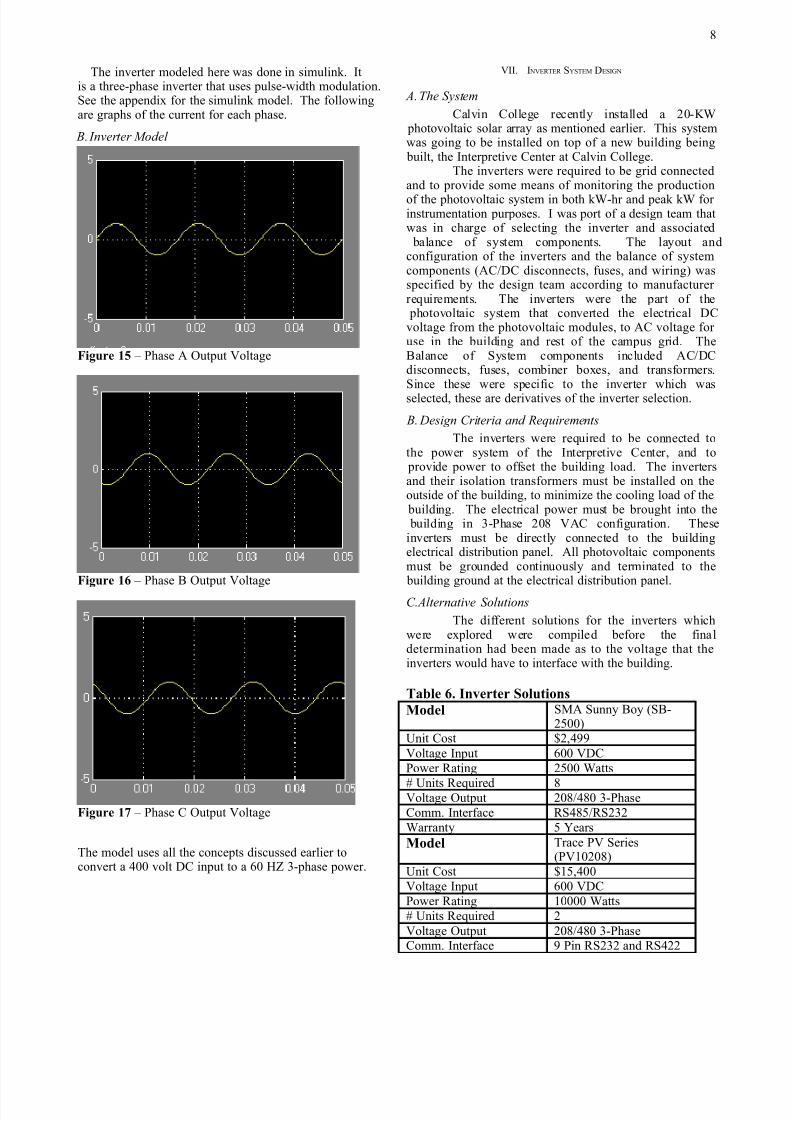
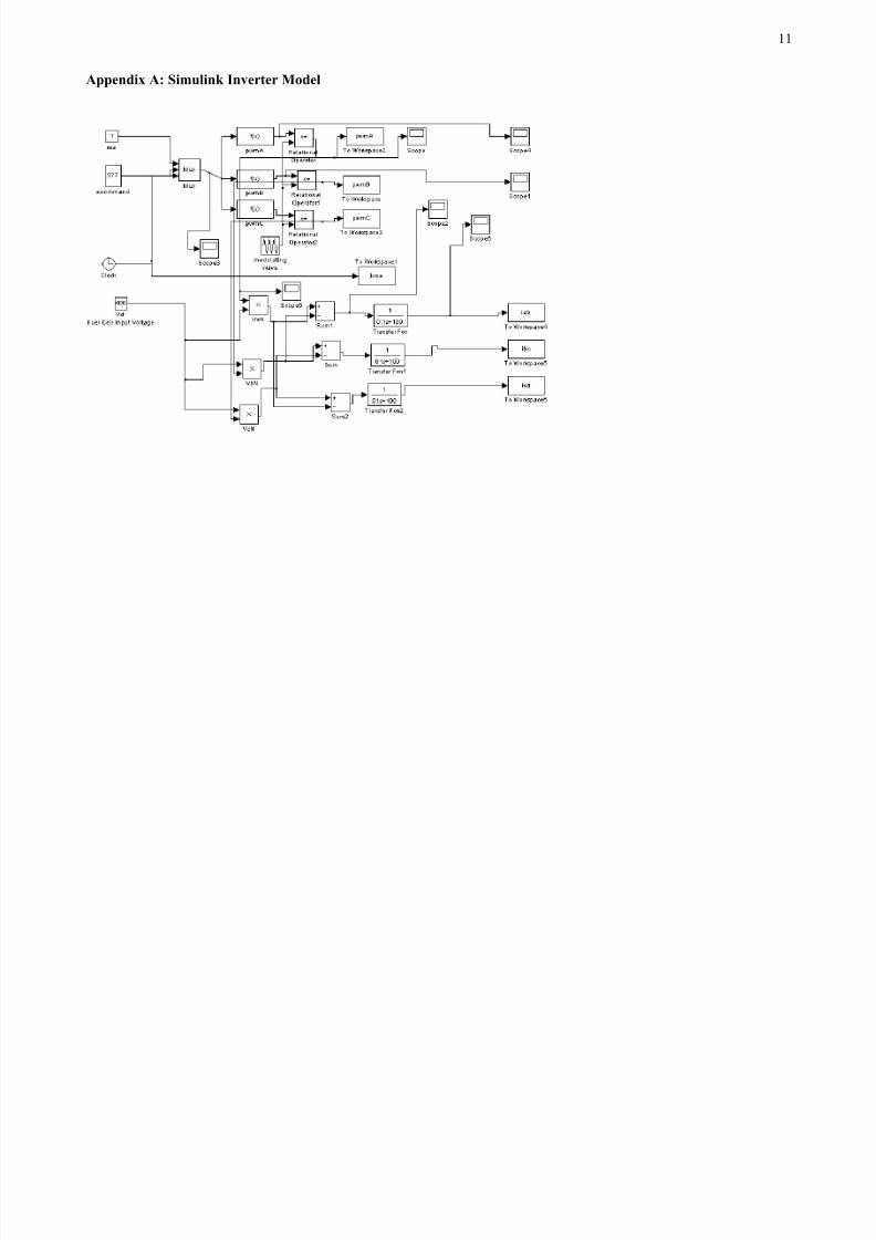
The inverter modeled here was done in simulink. Itis a three-phase inverter that uses pulse-width modulation.See the appendix for the simulink model. The followingare graphs of the current for each phase.
B. Inverter Model
Figure 15 – Phase A Output Voltage
Figure 16 – Phase B Output Voltage
Figure 17 – Phase C Output Voltage
The model uses all the concepts discussed earlier toconvert a 400 volt DC input to a 60 HZ 3-phase power.
VII. I NVERTER SYSTEM DESIGN
A. The System
Calvin College recently installed a 20-KW photovoltaic solar array as mentioned earlier. This systemwas going to be installed on top of a new building being built, the Interpretive Center at Calvin College.
The inverters were required to be grid connectedand to provide some means of monitoring the production
of the photovoltaic system in both kW-hr and peak kW for instrumentation purposes. I was port of a design team thatwas in charge of selecting the inverter and associated balance of system components. The layout andconfiguration of the inverters and the balance of systemcomponents (AC/DC disconnects, fuses, and wiring) wasspecified by the design team according to manufacturer requirements. The inverters were the part of the photovoltaic system that converted the electrical DCvoltage from the photovoltaic modules, to AC voltage for use in the building and rest of the campus grid. TheBalance of System components included AC/DCdisconnects, fuses, combiner boxes, and transformers.Since these were specific to the inverter which wasselected, these are derivatives of the inverter selection.
B. Design Criteria and Requirements
The inverters were required to be connected tothe power system of the Interpretive Center, and to provide power to offset the building load. The invertersand their isolation transformers must be installed on theoutside of the building, to minimize the cooling load of the building. The electrical power must be brought into the building in 3-Phase 208 VAC configuration. Theseinverters must be directly connected to the buildingelectrical distribution panel. All photovoltaic componentsmust be grounded continuously and terminated to the building ground at the electrical distribution panel.
C.Alternative Solutions
The different solutions for the inverters whichwere explored were compiled before the finaldetermination had been made as to the voltage that theinverters would have to interface with the building.
Table 6. Inverter Solutions
Model SMA Sunny Boy (SB-2500)
Unit Cost $2,499Voltage Input 600 VDCPower Rating 2500 Watts
# Units Required 8Voltage Output 208/480 3-PhaseComm. Interface RS485/RS232Warranty 5 Years
Model Trace PV Series(PV10208)
Unit Cost $15,400Voltage Input 600 VDCPower Rating 10000 Watts# Units Required 2Voltage Output 208/480 3-PhaseComm. Interface 9 Pin RS232 and RS422
8
8/6/2019 Clint Inverter Paper
http://slidepdf.com/reader/full/clint-inverter-paper 9/13
Warranty 5
Model Trace SunTie XR (ST-2000)
Unit Cost $2,100Voltage Input 48 VDCPower Rating 2000 Watts# Units Required 10Voltage Output 120 V 1-Phase
Comm. Interface 9 Pin RS232Warranty 5 Years
Model Trace SW Series (SW-5548)
Unit Cost $3,196Voltage Input 48 VDCPower Rating 5500 Watts# Units Required 4Voltage Output 120 V 1-PhaseComm. Interface RJ11-Serial PortWarranty 5 Years
Model Outback Powre (FX2548)
Unit Cost $2,245Voltage Input 48 VDCPower Rating 2,500 Watts# Units Required 8Voltage Output 120 V 1-PhaseComm. Interface RJ45Warranty 2 Years
These options contained the primary inverters thatare used for grid-tied photovoltaic systems. It was for thisreason that they were investigated. Historically photovoltaic systems have been utilized mainly instandalone applications; as a result there were many moreinverters available for small scale off-grid applications
[5,6]. D.Analysis of Alternatives
The different alternatives which were listed abovewere rated as to their capability to meet a number of criteria, including costs, software interface, voltage,efficiency, PV module compatibility and warranty. Thethree inverters which were not 3-Phase capable wereignored as viable solutions because of the requirement tointerface directly with the building power system.
E.Decision
The decision was made to use two Trace PVSeries 10208 10kW inverters. We required two of these
inverters, one for each side of the roof. This allowed us tomonitor each roof separately since the two systems wereelectrically isolated from each other.
F.Test and Integration
Once the inverters and the entire photovoltaicsystem had been installed, (including the inverters and the balance of system components) the system was inspected by the city of Grand Rapids electrical inspector. Uponcompletion of this inspection a Grid-Interconnect studywas completed for Consumers Energy. Upon approval by both of these agencies the photovoltaic system was
brought online. Testing of the inverters prior toinstallation was accomplished by connecting them to athree-phase AC source, and reading in the ac parameters.Detection of DC parameters was not possible since a largeDC source was not available.
G.Implementation
The photovoltaic manufacturer provided a package including all of the balance of system
components. Specifics regarding the wire size and conduitlocations were determined and provided to the PhysicalPlant Department and the Wolverine Construction/BuistElectrical Contractors by way of the Large-ScalePhotovoltaic Demonstration Project Drawing Set. SinceUni-Solar utilized a new MC Connect termination on their photovoltaic modules, it was decided by Don Winkle thePhysical Plant Electrician that these same connectorsshould be used throughout the system.
VIII.CONCLUSION
Inverters are a practical device and are a useful piece of equipment for many different applications. Anyone who
wants to run a laptop or other electronic device within acar or RV an inverter is required. Inverter types can becategorized by output waveform, switch type, switchingtechnology and frequency. In order to go from a constantDC voltage to an AC the input DC voltage is put throughan oscillating circuit which creates the output AC. Theoutput of the inverter can be a square wave, or a sinewave.
IX. R EFERENCES
[1] Ned Mohan, Tore M. Undeland, William P. RobbinsPower Electronics: Converters, Applications, and Design. 1989. JohnWiley & Sons, Inc.[2] McGraw-Hill Companies, Inc.
Principles and Applications of Engineering, Thomas Casson, 2000.[3] Narain G. Hingorani, Laszlo Gyugyi.Understanding Facts. The Institute of Electrical and ElectronicsEngineers, Inc. New York, 1999.[4] B.M. Bird, K.G. King, D.A.G. Pedder Introduction to Power Electronics. Wiley
New York, NY, 1993.[5] Xantrex Inverters. Datasheets and Inverter Specs.http://www.xantrex.com[6] Sunny Boy Inverters. Datasheets and Inverter Specs.http://www.sma.com[7] Nariain G. Hingorani, Laszlo Gyugyi.Understanding Facts Concepts and Technology of Flexible ACTransmission Systems. IEEE Press, Piscataway, NJ. 1995.
9

8/6/2019 Clint Inverter Paper
http://slidepdf.com/reader/full/clint-inverter-paper 10/13
Appendix
10
8/6/2019 Clint Inverter Paper
http://slidepdf.com/reader/full/clint-inverter-paper 11/13
Appendix A: Simulink Inverter Model
11

8/6/2019 Clint Inverter Paper
http://slidepdf.com/reader/full/clint-inverter-paper 12/13
Appendix B:
clear
format compact
global m n b w ma
%%%%%%%%%%%% Enter values for these parameters %%%%%%%%%%%%%
mf=72.203 % freq. modulation ratio (odd integer)
ma=0.339 % amplitude modulation ratio (1 or less)vdc=500 % input dc source voltage
fo=60 % fundamental frequency (of sine reference)nmax=mf*6 + 10 %number of terms to analyze in the Fourier series
r= 10 % resistance for series RL load
l=.02 % inductance in henries for series RL load
%%%%%%%%%%%%%%%%%%%%%%%%%%%%%%%%%%%%%%%%%%%%%%%%%%%%%%%%%%%%
fc=fo*mf
w=2*pi*fop= (mf+1)/2; % pulses per half cycle of sine
%calculate slope and intercept of each line segment of the triangular carrier signal
for n=1:2*p,m(n)=4*fc*(-1)^n ;
b(n)=(2*n-2)*(-1)^(n+1);
end
%calculate alpha for each pulse
for n=1:p,
alpha(n) = w*fzero('alphacalc',10e-3);
end
%calculate end of each pulse (alpha+delta)
for n=1:p,
alpdelta(n)= w*fzero('alpdelta',1e-3);end
%calc Fourier coefficients for Fbn
for n=1:nmax,
fb(n)=0 ;
for k=1:p,
fb(n)=fb(n) + (2*vdc/(n*pi))*(cos(n*alpha(k)) - cos(n*alpdelta(k)));end
end
for n=1:nmax,
for k=1:(p-1) ;
fb(n)=fb(n)+(2*vdc/(n*pi))*(cos(n*alpha(k+1)) - cos(n*alpdelta(k)));
endend
for n=1:nmax,v(n)= abs(fb(n));
end
%%%%%%%%%%%%%%%%%%%%%%%%%%%%%%%%%%%%%%%%%%%%%%%%%%%%%%%%%%%%%%%%%%%LOAD CURRENT: SERIES R-L LOAD
%calculate current, impedance, power at each frequencyfor n = 1:nmax
irms(n) = (v(n)/sqrt(2)) / sqrt( r^2 + (n*w*l)^2) ;
ipeak(n) = irms(n)*sqrt(2);power(n)=irms(n)^2*r;
z(n) = sqrt(r^2+(n*w*l)^2);end
I1rms = irms(1) %rms of fundamental
power_total=sum(power)
% calculate total harmonic distortion for the current
sumsquares=0;
for n = 2:nmax
12

8/6/2019 Clint Inverter Paper
http://slidepdf.com/reader/full/clint-inverter-paper 13/13
sumsquares = sumsquares + irms(n)^2;
endsqrt(sumsquares);
thd = sqrt(sumsquares)/irms(1)thdpercent = 100*thd
%% Graphs
subplot(2,1,1); bar(v), title(['voltage amplitude: Vdc = ',num2str(vdc),', ma = ',num2str(ma),', mf =',num2str(mf)])
subplot(2,1,2); bar(ipeak), title(['current amplitude: THD = ',num2str(thdpercent,'%11.2g'),' %'] )
%% This function is used by pwmbp1.m%alpha + delta for pwm
function y = f(x)
global m n b w ma
y = m(2*n)*x + b(2*n) - ma*sin(w*x);
% This function is used by pwmbp1.m
function y = f(x)
global m n b w ma
y=m(2*n-1)*x + b(2*n-1) - ma*sin(w*x);
13