Embed Size (px)
Citation preview

7/28/2019 paper inverter
http://slidepdf.com/reader/full/paper-inverter 1/7
IOSR Journal of Engineering
May. 2012, Vol. 2(5) pp: 1000-1006
ISSN: 2250-3021 www.iosrjen.org 1000 | P a g e
Power Factor Improvement With High Efficiency Converters
P. YOHAN BABU, P.SURENDRA BABU, K. Ravi Chandrudu, G.V.P. Anjaneyulu
Abstract — New recommendations and future standards have increased the interest in power factor improvement circuits.
There are multiple solutions in which line current is sinusoidal. In addition, in the recent years, a great number of circuitshave been proposed with non sinusoidal line current. In the proposed circuit, the power factor is improved by using anauxiliary winding coupled to the transformer of a cascade DC/DC fly back converter. The auxiliary winding is placed
between the input rectifier and the low-frequency filter capacitor to serve as a magnetic switch to drive an input inductor.The proposed approach is primarily based on the concept of inductive effect, from which PFC cells composed of energy buffers and high-frequency signals are introduced. Since the DC/DC fly back converter is operated at high-switchingfrequency, the auxiliary windings produce a high frequency pulsating source such that the input current conduction angle is
significantly lengthened and the input current harmonics is reduced. Properly selecting an eligible PFC cell and inserting it in between input rectifier and dc-link capacitor can yield an SSC which can improve the input power factor significantly.
Key Words — PFC, DC/DC converter, SSC, THD
I. INTRODUCTION
In modern electronic products, including personalcomputers, computer peripherals, and test instruments,
AC/DC Converters have become the primary power supplies. The AC/DC converters use switching circuits toachieve high-power transfer efficiency and ac/dc converter
controllers can be designed flexibly. Improving power quality considerations requires two things: achieving high power factor and low high-frequency harmonics. Manystudies have examined the relevant issues and numerous
topologies have been proposed. The proposed solutions of these studies can be classified into two groups: thosedesigned such that the input line current is sinusoidal andthose designed such that it is non sinusoidal [23], [24]. Thegroup of topologies with the sinusoidal line current almostachieves the requirement of unity power factor but requires
a complex topology or control circuit [25], [26]. Thus, thesinusoidal line current topologies are more costly toimplement. Fig. 1 shows the block diagram of the ac/dcconverter with sinusoidal input line current. The AC/DC
converter with non sinusoidal line current employs a simpletopology, such as single-stage – single-switch, and costs lessin practical applications [28] – [31]. Although the circuits
[29] – [31] lack a unity power factor, they comply with IEC61000-3-2 [26]. A family of such circuits was described in[23] and [24]. In this family a boost circuit accompanied bya DC/DC converter was introduced to form the so-called
single-stage single-switch AC/DC converters. The familycircuits have PFC function, as illustrated in Fig. 2. Thisconcept successfully simplifies a conventional power-factor
corrector by changing it from two stages to one stage.However, this concept employs a bulk inductor in the boostsection, which occupies significant volume and weight. Thenew converter satisfies the input harmonic current limits
required by IEC 61000-3-2 and also has fast output
response. A multi winding transformer is employed in the proposed converter. The additional winding in the primary
side is known as a reset winding in the forward-typeconverter. The reset winding of the transformer replaces the
boost inductor presented in [28] – [31]. Moreover, the proposed converter design reduces the volume and weight of the magnetic material by almost half compared to existing boost-based single-stage PFC converters. Furthermore, thevoltage across the bulk capacitor can be reduced to areasonable value by adjusting the turn‘s ratio of the
windings and, therefore, this design can adapt to significantline voltage variation. Generally, single-stage PFCconverters meet the regulatory requirements regarding the
input current harmonics, but they do not improve the power factor and reduce the THD as much as their conventionaltwo-stage counterpart. The power factor could be as low as0.8, however, they still meet the regulation. In addition,although the single-stage scheme is especially attractive in
low cost and low power applications due to its simplified power stage and control circuit, major issues still exist, suchas low efficiency and high as well as wide-range
intermediate DC bus voltage stress [2], [3]. Another technique based on parallel connection of this dither signalis presented in [8]; however, the harmonic content can meet
the regulatory standard by a small margin. In [14], a newconcept of PFC is proposed to improve the efficiency of asingle-stage converter by preventing the input current or voltage stress due the PFC cell from being added to the
active switch. In this circuit, the dc/dc cell operates in DCMso that a series of discontinuous pulses is used to shape theinput inductor current and the PFC is achieved. As thecircuit uses resonance of circuit parameters to achieve PFC,the control of the power factor will be very sensitive to thevariation of components values. In this letter, a new
technique of PFC is proposed. The PFC cell is formed byconnecting the energy buffer ( LB) and an auxiliary winding( L3) coupled to the transformer of the dc/dc cell, betweenthe input rectifier and the low-frequency filter capacitor
used in conventional power converter. Since the dc/dc cell isoperated at high frequency, the auxiliary winding produces ahigh frequency pulsating source such that the input current
conduction angle is significantly lengthened and the input
7/28/2019 paper inverter
http://slidepdf.com/reader/full/paper-inverter 2/7
IOSR Journal of Engineering
May. 2012, Vol. 2(5) pp: 1000-1006
ISSN: 2250-3021 www.iosrjen.org 1001 | P a g e
current harmonics is reduced. The input inductor LBoperates in DCM such that a lower THD of the input current
can be achieved.
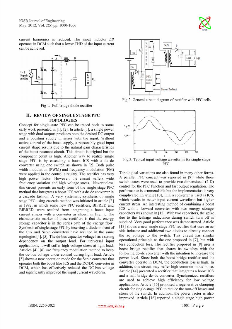
Fig 1: Full bridge diode rectifier
II. REVIEW OF SINGLE STAGE PFC TOPOLOGIES
Concept for single-state PFC can be traced back to someearly work presented in [1], [2]. In article [1], a single power stage with dual outputs produces both the desired DC outputand a boosting supply in series with the input. Without
active control of the boost supply, a reasonably good inputcurrent shape results due to the natural gain characteristicsof the boost resonant circuit. This circuit is original but the
component count is high. Another way to realize singlestage PFC is by cascading a boost ICS with a dc – dcconverter using one switch as shown in [2]. Both pulse
width modulation (PWM) and frequency modulation (FM)
were applied in the control circuitry. The rectifier has veryhigh power factor. However, the circuit suffers widefrequency variation and high voltage stress. Nevertheless,
this circuit presents an early form of the single stage PFCmethod that integrates a boost ICS with a dc – dc converter ina cascade fashion. A very systematic synthesis of single
stage PFC using cascade method was initiated in article [3]in 1992, in which some new PFC rectifiers, BIFRED andBIBRED, were resulted from integrating a boost inputcurrent shaper with a converter as shown in Fig. 1. Thecharacteristic marker of these rectifiers is that the energystorage capacitor is in the series path of the energy flow.Synthesis of single stage PFC by inserting a diode in front of
the Cuk and Sepic converters have resulted in the sametopologies [4], [5]. The dc-bus capacitor voltage has a strongdependency on the output load. For universal inputapplications, it will suffer high voltage stress at light load.
Articles [4], [6] use frequency modulation method to keepthe dc-bus voltage under control during light load. Article[5] shows a new operation mode for the Sepic converter that
operates both the boost like ICS and the DC/DC converter inDCM, which has effectively reduced the DC-bus voltageand significantly improved the input current waveform.
Fig 2: General circuit diagram of rectifier with PFC cells
Fig.3. Typical input voltage waveforms for single-stagePFC.
Topological variations are also found in many other forms.A parallel PFC concept was reported in [9], while three
switch-states were used to provide two-dimensional (2-D)control for the PFC function and fast output regulation. The performance is commendable but the implementation is very
complicated. In article [10], [11], a converter is used as ICS,which results in better input current waveform but higher current stress. An interesting method of combining a boostICS with a forward converter with two energy storage
capacitors was shown in [12]. With two capacitors, the spikedue to the leakage inductance during switch turn off is
subdued. Very good performance was demonstrated. Article[13] shows a new single stage PFC rectifier that uses an ac
side inductor and additional two diodes to directly connectthe ac voltage to the switch. This circuit has similar
operational principle as the one proposed in [7], but withless conduction loss. The rectifier proposed in [8] uses a boost bridge rectifier that shares its switches with thefollowing dc – dc converter with the intention to increase the
power level. Since both the boost bridge rectifier and theconverter operate in DCM, the conduction loss is high. Inaddition, this circuit may suffer high common mode noise.
Article [14] presented a rectifier that integrates a boost ICSand a half bridge dc – dc converter. Synchronized rectifiersare used to achieve high efficiency for low voltageapplications. Article [15] proposed a regenerative clamping
circuit for single-stage PFC to reduce the turn-off losses andstress of the switch. In addition, the power factor is alsoimproved. Article [16] reported a single stage high power
7/28/2019 paper inverter
http://slidepdf.com/reader/full/paper-inverter 3/7
IOSR Journal of Engineering
May. 2012, Vol. 2(5) pp: 1000-1006
ISSN: 2250-3021 www.iosrjen.org 1002 | P a g e
factor converter using the Sheppard – Taylor topology. Two possible operation regimes are described. Compared to the
usual boost-buck cascade operating in the first regime, the proposed converter has a wider operating range. When
operating in the second regime, the modified boost stage hasthe ability of producing a harmonic free input current, unlikethe standard boost PFC whose current always suffers a cuspdistortion. A new parallel approach for single stage PFC was
reported in [17] – [20] that employ an auxiliary dc/dcconverter to supplement energy to the load when the direct power from the line is low. This method improves overall
efficiency because only partial energy is processed twice.An additional switch is required. Extensive syntheses were performed in [21], [22] that yielded many families of singlestage PFC rectifiers based on dither effect [21] and partial
energy processing [22]. These two papers present interestingteaching from the principle of synthesis as well as analysis
to the implementation of the new circuits, thus are valuableto researchers in the power factor correction area.
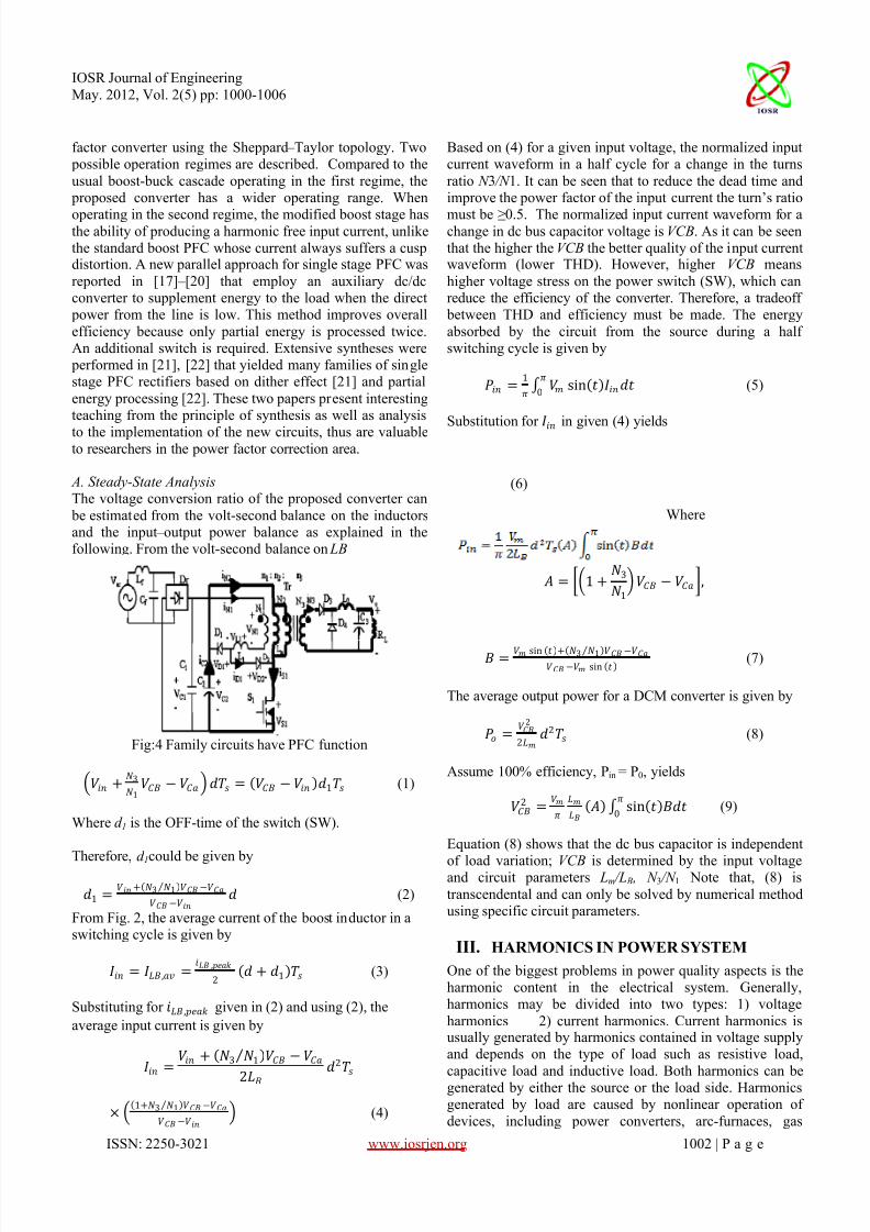
A. Steady-State AnalysisThe voltage conversion ratio of the proposed converter can
be estimated from the volt-second balance on the inductorsand the input – output power balance as explained in thefollowing. From the volt-second balance on LB
Fig:4 Family circuits have PFC function
+ 31 − = − 1 (1)
Where d 1 is the OFF-time of the switch (SW).
Therefore, d 1could be given by
1 = +3 1 −− (2)
From Fig. 2, the average current of the boost inductor in aswitching cycle is given by
= , = ,
2 + 1 (3)
Substituting for , given in (2) and using (2), the
average input current is given by
=
+ 3 1 − 2
2
× 1+3 1 −− (4)
Based on (4) for a given input voltage, the normalized inputcurrent waveform in a half cycle for a change in the turns
ratio N 3 /N 1. It can be seen that to reduce the dead time andimprove the power factor of the input current the turn‘s ratio
must be ≥ 0.5. The normalized input current waveform for achange in dc bus capacitor voltage is VCB. As it can be seenthat the higher the VCB the better quality of the input currentwaveform (lower THD). However, higher VCB means
higher voltage stress on the power switch (SW), which canreduce the efficiency of the converter. Therefore, a tradeoff between THD and efficiency must be made. The energy
absorbed by the circuit from the source during a half switching cycle is given by
=1
sin0
(5)
Substitution for
in given (4) yields
(6)
Where
= 1 + 3
1
− ,
= sin +3 1 −− sin (7)
The average output power for a DCM converter is given by
= 22 2 (8)
Assume 100% efficiency, Pin = P0, yields
2 =
sin
0(9)
Equation (8) shows that the dc bus capacitor is independent
of load variation; VCB is determined by the input voltageand circuit parameters Lm /L B , N 3 /N 1 Note that, (8) is
transcendental and can only be solved by numerical methodusing specific circuit parameters.
III. HARMONICS IN POWER SYSTEM
One of the biggest problems in power quality aspects is theharmonic content in the electrical system. Generally,harmonics may be divided into two types: 1) voltage
harmonics 2) current harmonics. Current harmonics isusually generated by harmonics contained in voltage supplyand depends on the type of load such as resistive load,
capacitive load and inductive load. Both harmonics can begenerated by either the source or the load side. Harmonicsgenerated by load are caused by nonlinear operation of
devices, including power converters, arc-furnaces, gas
7/28/2019 paper inverter
http://slidepdf.com/reader/full/paper-inverter 4/7
IOSR Journal of Engineering
May. 2012, Vol. 2(5) pp: 1000-1006
ISSN: 2250-3021 www.iosrjen.org 1003 | P a g e
discharge lighting devices, etc. Load harmonics can causethe overheating of the magnetic cores of transformer and
motors. On the other hand, source harmonics are mainlygenerated by power supply with non-sinusoidal voltage
waveform. Voltage and current source harmonics imply power losses, Electromagnetic Interference (EMI) and pulsating torque in AC motor drives. Any periodicwaveform can be shown to be the superposition of a
fundamental and a set of harmonic components. By applyingFourier transformation, these components can be extracted.The frequency of each harmonic component is an integral
multiple of its fundamental. There are several methods toindicate of the quantity of harmonics contents. The mostwidely used measure in North America is the totalharmonics distortion (THD), which is defined in terms of
the amplitudes of the harmonics, Hn, at frequency nw0,where w0 is frequency of the fundamental component whose
amplitude of H1 and n is integer. The THD ismathematically given by
= Hm=2 (n)2
1 (10)
IV. LINEAR AND NON-LINEAR LOADS
A linear element in a power system is a component in whichthe current is proportional to the voltage. In general, thismeans that the current wave shape will be the same as the
voltage (See Figure 5, 6, 7). Typical examples of linear loads include motors, heaters and incandescent lamps
Fig 5: Voltage and current waveforms for linear loads
Fig 6: – Voltage and current waveforms for non-linear loads
Fig 7: Waveform with symmetrical harmonic component
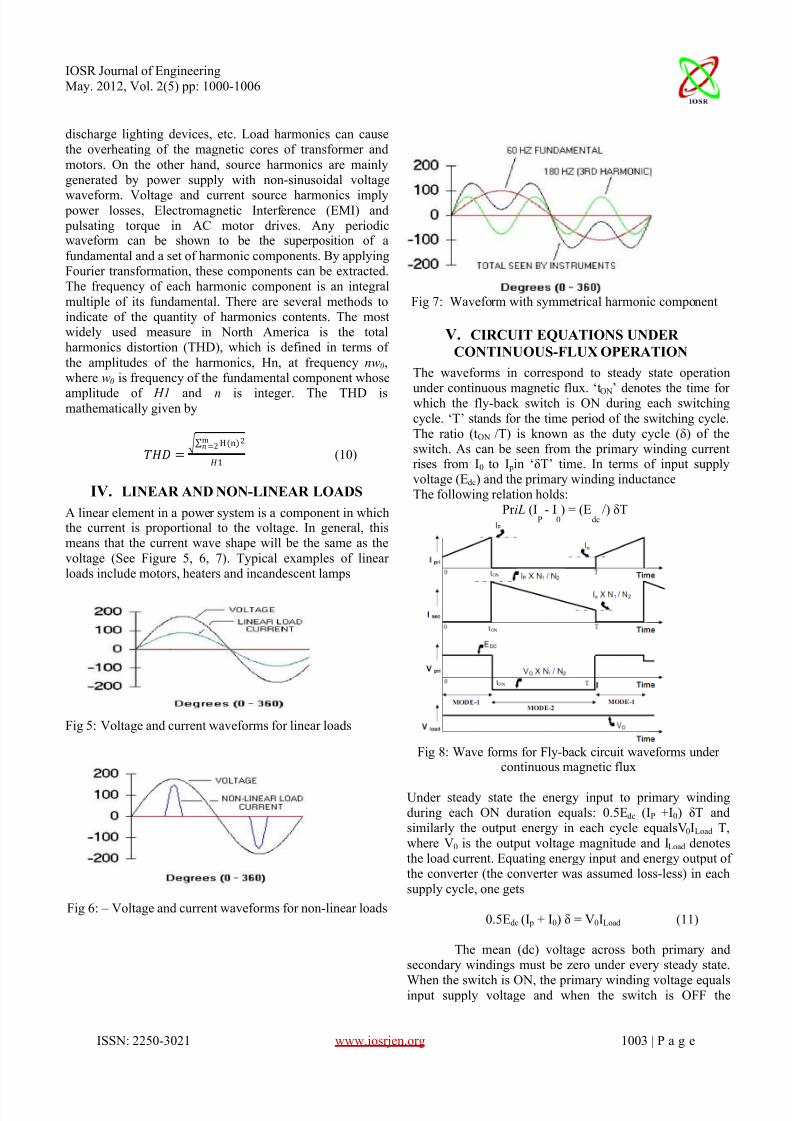
V. CIRCUIT EQUATIONS UNDER
CONTINUOUS-FLUX OPERATION
The waveforms in correspond to steady state operation
under continuous magnetic flux. ‗tON‘ denotes the time for which the fly-back switch is ON during each switching
cycle. ‗T‘ stands for the time period of the switching cycle.The ratio (tON
/T) is known as the duty cycle (δ) of the
switch. As can be seen from the primary winding currentrises from I0
to I pin ‗δT‘ time. In terms of input supply
voltage (Edc) and the primary winding inductanceThe following relation holds:
Pr iL (IP
- I0) = (E
dc/) δT
Fig 8: Wave forms for Fly-back circuit waveforms under continuous magnetic flux
Under steady state the energy input to primary windingduring each ON duration equals: 0.5Edc
(IP
+I0) δT and
similarly the output energy in each cycle equalsV0ILoad T, where V0
is the output voltage magnitude and ILoad
denotes
the load current. Equating energy input and energy output of the converter (the converter was assumed loss-less) in each
supply cycle, one gets
0.5Edc (I p + I0) δ = V0ILoad (11)
The mean (dc) voltage across both primary andsecondary windings must be zero under every steady state.
When the switch is ON, the primary winding voltage equalsinput supply voltage and when the switch is OFF the
7/28/2019 paper inverter
http://slidepdf.com/reader/full/paper-inverter 5/7
IOSR Journal of Engineering
May. 2012, Vol. 2(5) pp: 1000-1006
ISSN: 2250-3021 www.iosrjen.org 1004 | P a g e
reflected secondary voltage appears across the primarywinding. Under the assumption of ideal switch and diode.
Edcδ = (N1 / N2) V1 (1-δ) (12)
Where N1
and N2
are the number of turns in
primary and secondary windings and (N1 / N2) V0 is the
reflected secondary voltage across the primary winding(dotted end of the windings at lower potential) during mode-2 of circuit operation. One needs to know the requiredratings for the switch and the diode used in the converter.
When the switch is OFF, it has to block a voltage (VSWITCH)that equals to the sum of input voltage and the reflectedsecondary voltage during mode-2. Thus,
VSwitch = Edc
+ (N1
/ N2) V0 (13)
When the switch in ON, the diode has to block a voltage(Vdiode) that equals to the sum of output voltage andreflected primary voltage during mode-1, i.e.,
Vdiode = V0
+ Edc
(N2
/ N1) (14)
Fig 9: Fly-back circuit waveforms under discontinuous
magnetic flux
With the turning ON of the switch, the primary winding
current starts building up linearly from zero and at the endof mode-1 the magnetic field energy due to primary windingcurrent rises to 212 priPLI . This entire energy is transferredto the output at the end of mode-2 of circuit operation.
Under the assumption of loss-less operation the output power (P
o) can be expressed as
P0 = 21/2 priPLI switch
(15)Where Fswitch=1/T is the switching frequency of theconverter. It may be noted that output power P0
is same as
V0ILoad used in Equation (11). The volt-time area equation asgiven in Eqn.(12) gets modified under discontinuous fluxmode of operation as follows
Edc δ ≤ (N1
/N2) V0
(1-δ) (16)
Average voltage across windings over a switching cycle isstill zero. The inequality sign of Eqn.16 is due to the fact
that during part of the OFF period of the switch [= (1-δ)T],the winding voltages are zero. This zero voltage duration
had been identified earlier as mode-3 of the circuitoperation.
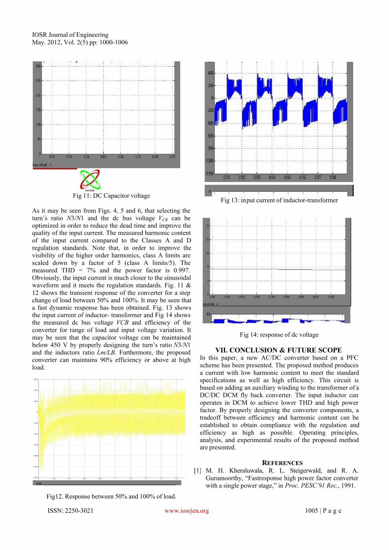
VI. RESULT ANALYSISIn order to verify the proposed concept, a prototype of theconverter shown in Fig. 2 was constructed andexperimentally tested. To ensure proper operation of the
converter, the dc bus voltage (VCB) must be higher than theinput voltage, such that the diode D1 is OFF and theinductor LB stores energy when the switch (SW) is ON.Therefore, from (15) the inductor Lm must be higher than
the input inductor LB. The DCM converter was designedand implemented for 50 V/80 W output, V in ,rms (100 – 240
V) universal line voltage, and overall efficiency of 86% isassumed. The switching frequency is selected to be 100 kHzand the maximum duty cycle of is 0.45.
Fig 10: input current& input voltage measurement at dioderectifier
Fig.10 shows the measured input voltage and filtered inputcurrent waveforms for a 100 Vac input voltage at full load.
7/28/2019 paper inverter
http://slidepdf.com/reader/full/paper-inverter 6/7
IOSR Journal of Engineering
May. 2012, Vol. 2(5) pp: 1000-1006
ISSN: 2250-3021 www.iosrjen.org 1005 | P a g e
Fig 11: DC Capacitor voltage
As it may be seen from Figs. 4, 5 and 6, that selecting theturn‘s ratio N 3 /N 1 and the dc bus voltage V CB can beoptimized in order to reduce the dead time and improve thequality of the input current. The measured harmonic content
of the input current compared to the Classes A and Dregulation standards. Note that, in order to improve thevisibility of the higher order harmonics, class A limits are
scaled down by a factor of 5 (class A limits/5). Themeasured THD = 7% and the power factor is 0.997.Obviously, the input current is much closer to the sinusoidalwaveform and it meets the regulation standards. Fig. 11 &
12 shows the transient response of the converter for a stepchange of load between 50% and 100%. It may be seen thata fast dynamic response has been obtained. Fig. 13 showsthe input current of inductor- transformer and Fig 14 showsthe measured dc bus voltage VCB and efficiency of theconverter for range of load and input voltage variation. It
may be seen that the capacitor voltage can be maintained below 450 V by properly designing the turn‘s ratio N 3 /N 1and the inductors ratio Lm/LB. Furthermore, the proposedconverter can maintains 90% efficiency or above at high
load.
Fig12. Response between 50% and 100% of load.
Fig 13: input current of inductor-transformer
Fig 14: response of dc voltage
VII. CONCLUSION & FUTURE SCOPEIn this paper, a new AC/DC converter based on a PFCscheme has been presented. The proposed method produces
a current with low harmonic content to meet the standardspecifications as well as high efficiency. This circuit is
based on adding an auxiliary winding to the transformer of aDC/DC DCM fly back converter. The input inductor can
operates in DCM to achieve lower THD and high power factor. By properly designing the converter components, atradeoff between efficiency and harmonic content can beestablished to obtain compliance with the regulation and
efficiency as high as possible. Operating principles,analysis, and experimental results of the proposed methodare presented.
R EFERENCES
[1] M. H. Kheraluwala, R. L. Steigerwald, and R. A.
Gurumoorthy, ―Fastresponse high power factor converter with a single power stage,‖ in Proc. PESC’91 Rec., 1991.
7/28/2019 paper inverter
http://slidepdf.com/reader/full/paper-inverter 7/7
IOSR Journal of Engineering
May. 2012, Vol. 2(5) pp: 1000-1006
ISSN: 2250-3021 www.iosrjen.org 1006 | P a g e
[2] I. Takahashi and R. Y. Igarashi, ―A switching power supply of 99% power factor by the dither
rectifier,‖ in Proc. 13th Int. Telecommun. EnergyConf. —INTELEC’91, 1991, pp. 714 – 719.
[3] M. Madigan, R. Erickson, and E. Ismail,―Integrated high quality rectifier - regulators,‖ in PESC’92, pp. 1043 – 1051.
[4] M. Brkovic and S. Cuk, ―Automatic current shaper
with f ast output regulation and soft switching,‖ in Proc. INTELEC’93, 1993, pp. 379 – 386.
[5] K. Schenk and S. Cuk, ―A single-switch single-
stage active power factor corrector with highquality input and output,‖ in Proc. PESC’97
Rec.,1997.[6] M. M. Jovanovic, D. M. Tsang, and F. C. Lee,
―Reduction of voltage stress in integrated high-quality rectifier-regulators by variable frequency
control,‖ in Proc. IEEE APEC , 1994, pp. 569 – 575.[7] R. Redl, L. Balogh, and N. O. Sokal, ―A new
family of single-stage isolated power-factor correctors with fast regulation of the outputvoltage,‖ in Proc. PESC’94, pp. 1137 – 1144.
[8] E. Rodriguez, F. Canales, P. Najera, and J. Arau,―A novel isolated high quality rectifier with fastdynamic output response,‖ in Proc. PESC’97 , vol.
1., 1997, pp. 550 – 555.[9] Y. Jiang and F. C. Lee, ―Single-stage single-phase
parallel power factor correction scheme,‖ in Proc.
PESC’94, vol. 2, 1994, pp. 1145 – 1151.
[10] Z. Lai and K. M. Smedley, ―A single-stage power-
factor-corrected AC – DC converter with fast outputregulation and improved current shaping,‖ in Proc.
12th Int. HFPC Power Conv., 1997, pp. 51 – 62.[11] P. Kornetzky, H. Hei, and I. Batarseh, ―A novel
one-stage power factor correction converter,‖ in
Proc. APEC’97 , vol. 1, 1997, pp. 251 – 258.[12] P. Kornetzky, H.Wei, G. Zhu, and I. Batarseh, ―A
single-switch AC/DC converter with power factor correction,‖ in Proc. PESC’97 , vol. 1, 1997, pp.
527 – 535.[13] Y. K. Cha, M. H. Ryu, B. C. Choi, and H. G. Kim,
―Single stage ac/dc converter with low conduction
loss and high power factor,‖ in PES C’98,1998,
(acL), pp. 1362 – 1367.[14] J.-Y. Lee, G.-W. Moon, and M.-J. Youn, ―Design
of high quality AC/DC converter with highefficiency based on half bridge topology,‖ in Proc.PESC’98, 1998, synrectifier, pp. 1054 – 1060.
[15] Y. S. Lee, K. W. Siu, and B. T. Lin, ―Novel single-
stage isolated powerfactor- corrected power supplies with regenerative clamping,‖ in
Proc.APEC’97 , 1997, pp. 259 – 265.[16] Tse and Chow , ―Single stage high power factor
converter using the Sheppard-Taylor topology,‖ in Proc. PESC’96 , 1996.
[17] O. Garcia, J. A. Cobos, P. Alou, R. Prieto, J.
Uceda, and S. Ollero, ―A new family of singlestage ac/dc power factor correction converters with
fast output voltage regulation,‖ in Proc. PESC’97 ,vol. 1, 1997, pp.536 – 542.
[18] ―A high efficient low output voltage (3.3 v) single-stage ac/dc power factor correction converter,‖ in
Proc. APEC’98, 1998, pp. 201 – 207.[19] ―A new approach for single stage AC/DC power
factor correction converters with an improvedenergy processing,‖ in Proc. P ESC’98, 1998, pp.
1061 – 1067.[20] E. Rodriguez, O. Garcia, J. A. Cobos, J. Arau, and
J. Uceda, ―A singlestage rectifier with PFC and fast
regulation of the output voltage,‖ in Proc. PESC’98, 1998, pp. 1642 – 1648.
[21] T. F. Wu, T.-H. Yu, and Y. C. Liu, ―Principle of synthesizing singlestage converters for off-line
applications,‖ in Proc. APEC’98, 1998, pp. 427 – 433.
[22] T. F. Wu, Y.-J. Wu, and Y. C. Liu, ―Developmentof converters for improving efficiency andachieving both power factor correction and fastoutput regulation,‖ in Proc. APEC’99, 1999.
[23] O. Garcia, J. A. Cobos, R. Prieto, P. Alou, and J.
Uceda, ―Power factor correction: a survey,‖ in Proc. IEEE PESC’01, 2001, pp. 8 – 13.
[24] C. Qiao and K. M. Smedley, ―A topology survey of
single-stage power factor corrector with a boosttype input-current-shaper,‖ in Proc. IEEE
APEC’00, 2000, pp. 460 – 467.[25] L. Dixon Jr, ―High power factor pre regulators for
off-line supplies,‖ presented at the Unitrode Power
Supply Design Seminar, 1991, Paper I2.[26] M. H. L. Chow, Y. S. Lee, and C. K. Tse, ―Single-
stage single-switch isolated PFC regulator withunity power factor, fast transient response and lowvoltage stress,‖ in Proc. IEEE PESC’98, 1998, pp.
1422 – 1428.[27] Electromagnetic Compatibility (EMC), Part 3,
International Standard IEC61000-3-2, 2001.[28] R. Redl, L. Balogh, and N. Sokal, ―A new family
of single-stage isolated power-factor correctconverter with fast regulation of the outputvoltage,‖ in Proc. IEEE PESC’94, 1994, pp. 1137 –
1144.
[29] L. Huber and M. M. Jovanovic, ―Single stagesingle switch isolated power supply technique with
input current shaping and fast output voltageregulation for universal input voltage rangeapplication,‖ in Proc. IEEE APEC’97 , 1997, pp.272 – 280.
[30] F. S. Tsai, P. Markowski, and E. Whitcomb, ―Off -line flyback converter with input harmonic currentcorrection,‖ in Proc. IEEE INTELEC’96 , 1996, pp.120 – 124.
[31] J. Sebastián, M. M. Hernando, P. Villegas, J. Diaz,and A. Fontán, ―Input current sharper based on theseries connection of a voltage source and a loss free
resistor,‖ in Proc. IEEE APEC’98, 1998, pp. 461 – 467.