Embed Size (px)
Citation preview
General DescriptionThe MAX14748 USB battery charger integrates a charger detector, boost/buck converter, and Li+ battery charger with smart power selector to provide fast and safe charging of 2s Li+ battery packs.The MAX14748 provides support for devices functioning as a UFP/DRP per the USB Type-C 1.1 standard, while also providing detection of legacy USB Battery Charging Specification, Revision 1.2 (BC1.2) compliant chargers in addition to other nonstandard chargers. The programmable Automatic Input Current Limiting (AICL) feature ensures that maximum safe current is drawn from the charging adapter.The Li+ charger includes an automatic Smart Power Selector™ to simultaneously charge the battery and provide power to the system load. The Smart Power Selector function will supplement the system power with the battery if power from the charging adapter is insufficient. The Li+ charger features JEITA thermal monitoring and charger voltage/current reduction or charger disable.The MAX14748 is available in a 54-bump, 0.4mm pitch, 3.97mm x 2.77mm x 0.64mm wafer-level package (WLP) and operates over the -40°C to +85°C extended temperature range.
Applications ● Digital Imaging (DSC, DVC) ● Wireless Speakers ● Handheld Barcode Readers
Benefits and Features ● Minimize Power Management Footprint Through High
Integration• 13mΩ (typ) Integrated Battery To System Switch• Thermal Current Limiting• DC-DC Converter with Boost and Reverse Buck• High Efficiency
- 92% in Boost Mode at 1A Output Current and 7.4V Battery Voltage
- 94% in Reverse Buck Mode at 500mA Output • Internal USB Switch for USB D+/D- Data Lines
● Easy-to-Implement Li+ Battery Charging• Charges 2s Li-Ion Batteries from Legacy 5V USB
Adapters - 15W Input Power with 3A Type-C Adapter - 7.5W Input Power with DCP Adapter - 1A System/Charge Current From DCP Adapter - 2A System/Charge Current From 3A Type-C Adapter
• DRP Mode USB Type-C Specification, Rev 1.1 Compliant
• UFP Mode USB Type-C Specification, Rev 1.1 Support
• VCONN and Super-Speed Multiplexer Logic Controls• Non-Standard DCP Detection• USB Battery Charging Specification, Rev 1.2 Compliant
● Automatic Input Current Limit (AICL) Power Management
● Support Weak/Dead Batteries Detection• Smart Power Selector• Thermistor Monitor
● Various Protection Features• 28V Integrated Overvoltage Protection• JEITA Charge Protection• ±15kV ESD Protection on USB Adapter Pins
Ordering Information appears at end of data sheet.
Smart Power Selector is a trademark of Maxim Integrated Products, Inc.
19-100081; Rev 3; 4/18
Click here for production status of specific part numbers.
MAX14748 USB Type-C Charger
Voltages Referenced to GNDCHGIN ..................................................................-0.3V to +30VBST .......................................................................-0.3V to +16VSYS to BAT ..........................................................-0.3V to +12V BAT, SYS ..............................................................-0.3V to +12VBYP to CHGIN ......................................................-30V to +0.3VBYP, THM, INT, SYSOK, FLTIN, FSUS,
LED, SDA, SCL ....................................................-0.3V to 6VCOMP, SET .......................................... -0.3V to VCCINT + 0.3VCC1, CC2, TDN, TDP, CDN, CDP, VCONN ............-0.3V to +6VCC1, CC2, in fault mode through a 10k resistor ..-0.3V to +20VCDIR .......................................................................-0.3V to +6VVTPU (VTPU-TPU switch open) .......... -0.3V to VCCINT + 0.3VTPU (VTPU-TPU switch open) .........-0.3V to 6 or VTPU + 0.3VVTPU, TPU Maximum Current
(VTPU-TPU switch closed) ...................... -100mA to +100mABVCEN ..................................................-0.3V to VCCINT + 0.3V
SFOUT, VCCINT, BREG ....... -0.3V to min ((VCHGIN + 0.3), 6)VLX .............................................................-0.3V to VSYS + 0.3VNVP ......................................................................-0.3V to +30VAGND, DGND, PGND, GND ...............................-0.3V to +0.3VContinuous Current into
CHGIN, SYS ...................................................................+6.4A BAT .................................................................................+4.8A Any Other Terminal .....................................................+100mAContinuous Power Dissipation
(multilayer board at +70°C): 9 x 6 Array 54-Bump, 3.97mm x 2.77mm 0.4mm Pitch WLP (derate 24.46mW/°C) .................................................1.957W
Operating Temperature Range .......................... -40°C to +85°CJunction Temperature ................................................... +150°CStorage Temperature Range ........................... -65°C to +150°CLead Temperature (soldering, 10s) .............................. +300°CSoldering Temperature (reflow) .................................... +260°C
(Note 1)WLP
Junction-to-Ambient Thermal Resistance (θJA) .....40.88°C/W
(VBAT = 8.3V, TA = -40°C to +85°C, all registers in their default state, unless otherwise noted. Typical values are at VCHGIN = 5.0V, VBAT =7.4V, VSYS = VBATREG, TA = +25°C.)
PARAMETER SYMBOL CONDITIONS MIN TYP MAX UNITS
SUPPLY CURRENT
BAT Supply Current IBAT
VCHGIN = 0V or Floating, Type-C detection active 140 µA
Low Power mode 25 µA
CHGIN Supply Current ICHG
VCHGIN = +5V, TA +25°C, ChgEn = 0 5.3 mA
VCHGIN = +5V, TA +25°C, Suspend Mode (FSUS = High) 0.98 mA
CHGIN TO BYP PATHAllowed CHGIN Input Voltage Range VCHGIN_RNG 0 28 V
CHGIN Detect Threshold
VBDET Rising 3.8 3.9 4.0V
VBDET_F Falling 3.6 3.7 3.8
CHGIN Overvoltage Threshold
VOVP Rising 5.59 5.66 5.72 VVOVP_F Falling 5.56 VVOVP_H Hysteresis 28 mV
MAX14748 USB Type-C Charger
www.maximintegrated.com Maxim Integrated │ 2
Note 1: Package thermal resistances were obtained using the method described in JEDEC specification JESD51-7, using a four-layer board. For detailed information on package thermal considerations, refer to www.maximintegrated.com/thermal-tutorial.
Absolute Maximum Ratings
Stresses beyond those listed under “Absolute Maximum Ratings” may cause permanent damage to the device. These are stress ratings only, and functional operation of the device at these or any other conditions beyond those indicated in the operational sections of the specifications is not implied. Exposure to absolute maximum rating conditions for extended periods may affect device reliability.
Package Thermal Characteristics
Electrical Characteristics
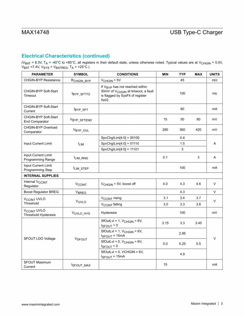
(VBAT = 8.3V, TA = -40°C to +85°C, all registers in their default state, unless otherwise noted. Typical values are at VCHGIN = 5.0V, VBAT =7.4V, VSYS = VBATREG, TA = +25°C.)
PARAMETER SYMBOL CONDITIONS MIN TYP MAX UNITSCHGIN-BYP Resistance RCHGIN_BYP VCHGIN = 5V 45 mW
CHGIN-BYP Soft-Start Timeout tBYP_SFTTO
If VBYP has not reached within 50mV of VCHGIN at timeout, a fault is flagged by SysFlt of register 0x02.
100 ms
CHGIN-BYP Soft-Start Current IBYP_SFT 60 mA
CHGIN-BYP Soft-Start End Comparator VBYP_SFTEND 15 50 80 mV
CHGIN-BYP Overload Comparator VBYP_OVL 290 360 420 mV
Input Current Limit ILIM
SpvChgILim[4:0] = 00100 0.4ASpvChgILim[4:0] = 01110 1.5
SpvChgILim[4:0] = 11101 3
Input Current Limit Programming Range ILIM_RNG 0.1 3 A
Input Current Limit Programming Step ILIM_STEP 100 mA
INTERNAL SUPPLIESInternal VCCINT Regulator VCCINT VCHGIN = 5V, boost off 4.0 4.3 4.6 V
Boost Regulator BREG VBREG 4.3 V
VCCINT UVLO Threshold VUVLO
VCCINT rising 3.1 3.4 3.7V
VCCINT falling 3.0 3.3 3.6
VCCINT UVLO Threshold Hysteresis VUVLO_HYS Hysteresis 100 mV
SFOUT LDO Voltage VSFOUT
SfOutLvl = 1, VCHGIN = 6V, ISFOUT = 0 3.15 3.3 3.45
V
SfOutLvl = 1, VCHGIN = 6V, ISFOUT = 15mA 2.95
SfOutLvl = 0, VCHGIN = 6V, ISFOUT = 0 5.0 5.25 5.5
SfOutLvl = 0, VCHGIN = 6V, ISFOUT = 15mA 4.9
SFOUT Maximum Current ISFOUT_MAX 15 mA
MAX14748 USB Type-C Charger
www.maximintegrated.com Maxim Integrated │ 3
Electrical Characteristics (continued)
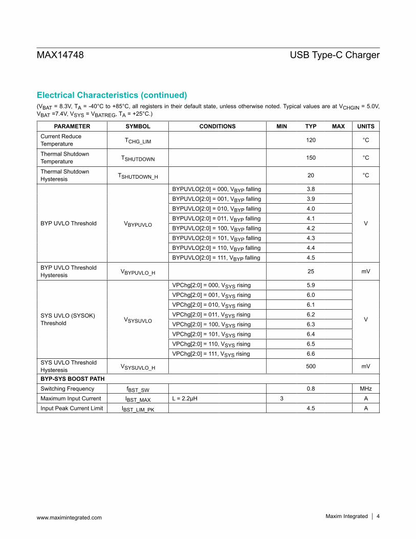
(VBAT = 8.3V, TA = -40°C to +85°C, all registers in their default state, unless otherwise noted. Typical values are at VCHGIN = 5.0V, VBAT =7.4V, VSYS = VBATREG, TA = +25°C.)
PARAMETER SYMBOL CONDITIONS MIN TYP MAX UNITSCurrent Reduce Temperature TCHG_LIM 120 °C
Thermal Shutdown Temperature TSHUTDOWN 150 °C
Thermal Shutdown Hysteresis TSHUTDOWN_H 20 °C
BYP UVLO Threshold VBYPUVLO
BYPUVLO[2:0] = 000, VBYP falling 3.8
V
BYPUVLO[2:0] = 001, VBYP falling 3.9BYPUVLO[2:0] = 010, VBYP falling 4.0BYPUVLO[2:0] = 011, VBYP falling 4.1BYPUVLO[2:0] = 100, VBYP falling 4.2BYPUVLO[2:0] = 101, VBYP falling 4.3BYPUVLO[2:0] = 110, VBYP falling 4.4BYPUVLO[2:0] = 111, VBYP falling 4.5
BYP UVLO Threshold Hysteresis VBYPUVLO_H 25 mV
SYS UVLO (SYSOK) Threshold VSYSUVLO
VPChg[2:0] = 000, VSYS rising 5.9
V
VPChg[2:0] = 001, VSYS rising 6.0VPChg[2:0] = 010, VSYS rising 6.1VPChg[2:0] = 011, VSYS rising 6.2VPChg[2:0] = 100, VSYS rising 6.3VPChg[2:0] = 101, VSYS rising 6.4VPChg[2:0] = 110, VSYS rising 6.5VPChg[2:0] = 111, VSYS rising 6.6
SYS UVLO Threshold Hysteresis VSYSUVLO_H 500 mV
BYP-SYS BOOST PATHSwitching Frequency fBST_SW 0.8 MHzMaximum Input Current IBST_MAX L = 2.2µH 3 AInput Peak Current Limit IBST_LIM_PK 4.5 A
MAX14748 USB Type-C Charger
www.maximintegrated.com Maxim Integrated │ 4
Electrical Characteristics (continued)
(VBAT = 8.3V, TA = -40°C to +85°C, all registers in their default state, unless otherwise noted. Typical values are at VCHGIN = 5.0V, VBAT =7.4V, VSYS = VBATREG, TA = +25°C.)
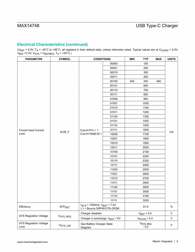
PARAMETER SYMBOL CONDITIONS MIN TYP MAX UNITS
Forced Input Current Limit IILIM_F CurLim1Frc = 1 ,
CurLim1Set[4:0] =
00000 100
mA
00001 20000010 30000011 40000100 405 450 49500101 60000110 70000111 80001000 90001001 100001010 110001011 120001100 130001101 140001110 150001111 160010000 170010001 180010010 190010011 200010100 210010101 220010110 230010111 240011000 250011001 260011010 270011011 280011100 290011101 300011110 310011111 3200
Efficiency EFFBSTISYS = 1000mA, VBAT = 7.4V, L1 = Bourns SRP4012TA-2R2M 91.6 %
SYS Regulation Voltage VSYS_REGCharger disabled VBAT + 0.4 V
Charger in precharge, VBAT = 5V VPCHG + 0.4 V
SYS Regulation Voltage Limit VSYS_LIM
See Battery Charger State Diagram
VSYS_REG - 0.2 V
MAX14748 USB Type-C Charger
www.maximintegrated.com Maxim Integrated │ 5
Electrical Characteristics (continued)
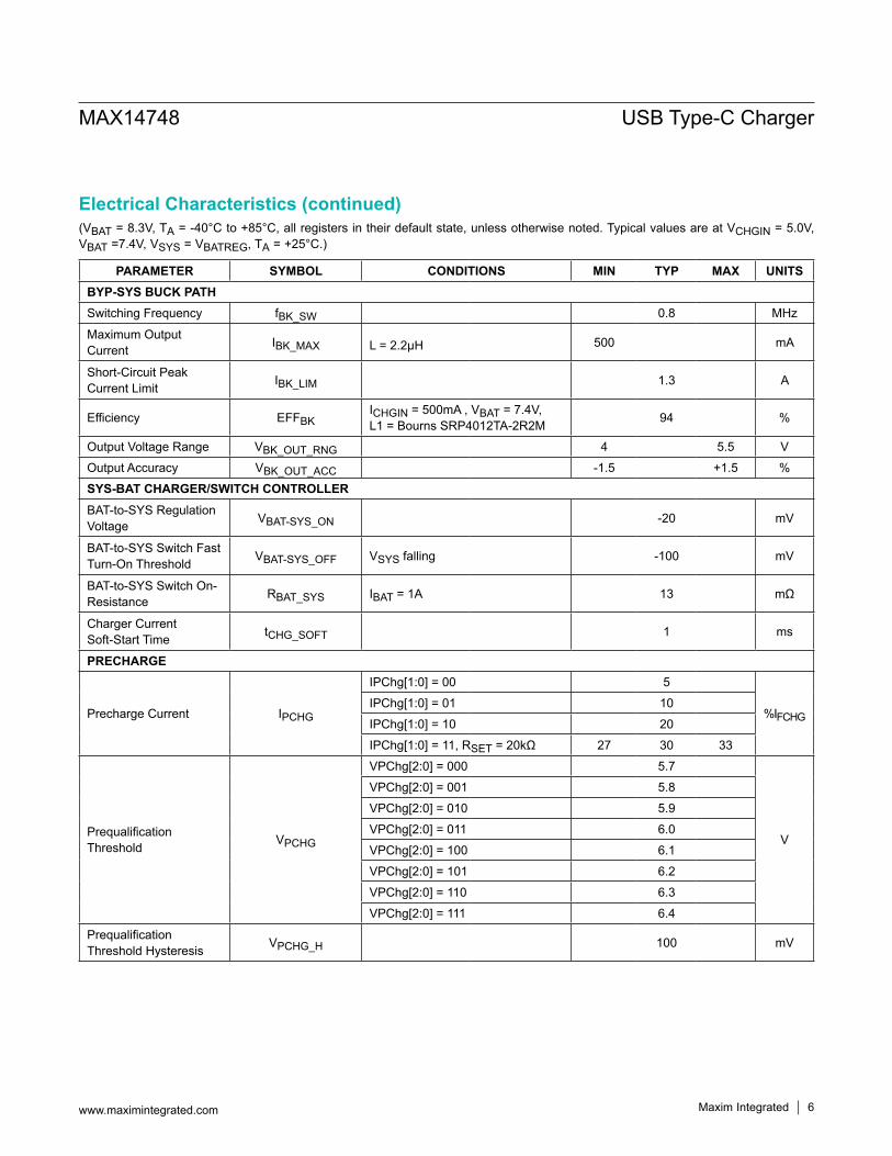
(VBAT = 8.3V, TA = -40°C to +85°C, all registers in their default state, unless otherwise noted. Typical values are at VCHGIN = 5.0V, VBAT =7.4V, VSYS = VBATREG, TA = +25°C.)
PARAMETER SYMBOL CONDITIONS MIN TYP MAX UNITSBYP-SYS BUCK PATHSwitching Frequency fBK_SW 0.8 MHz
Maximum Output Current IBK_MAX L = 2.2µH 500 mA
Short-Circuit Peak Current Limit IBK_LIM 1.3 A
Efficiency EFFBKICHGIN = 500mA , VBAT = 7.4V, L1 = Bourns SRP4012TA-2R2M 94 %
Output Voltage Range VBK_OUT_RNG 4 5.5 VOutput Accuracy VBK_OUT_ACC -1.5 +1.5 %SYS-BAT CHARGER/SWITCH CONTROLLERBAT-to-SYS Regulation Voltage VBAT-SYS_ON -20 mV
BAT-to-SYS Switch Fast Turn-On Threshold VBAT-SYS_OFF VSYS falling -100 mV
BAT-to-SYS Switch On-Resistance RBAT_SYS IBAT = 1A 13 mΩ
Charger Current Soft-Start Time tCHG_SOFT 1 ms
PRECHARGE
Precharge Current IPCHG
IPChg[1:0] = 00 5
%IFCHGIPChg[1:0] = 01 10IPChg[1:0] = 10 20IPChg[1:0] = 11, RSET = 20kΩ 27 30 33
Prequalification Threshold VPCHG
VPChg[2:0] = 000 5.7
V
VPChg[2:0] = 001 5.8VPChg[2:0] = 010 5.9VPChg[2:0] = 011 6.0VPChg[2:0] = 100 6.1VPChg[2:0] = 101 6.2VPChg[2:0] = 110 6.3VPChg[2:0] = 111 6.4
Prequalification Threshold Hysteresis VPCHG_H 100 mV
MAX14748 USB Type-C Charger
www.maximintegrated.com Maxim Integrated │ 6
Electrical Characteristics (continued)
(VBAT = 8.3V, TA = -40°C to +85°C, all registers in their default state, unless otherwise noted. Typical values are at VCHGIN = 5.0V, VBAT =7.4V, VSYS = VBATREG, TA = +25°C.)
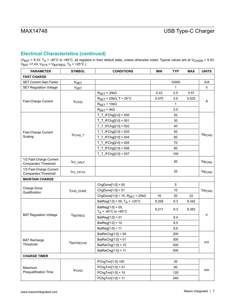
PARAMETER SYMBOL CONDITIONS MIN TYP MAX UNITSFAST CHARGESET Current Gain Factor KSET 10000 A/ASET Regulation Voltage VSET 1 V
Fast-Charge Current IFCHG
RSET = 20kΩ 0.43 0.5 0.57
ARSET = 20kΩ, T = 25°C 0.475 0.5 0.525RSET = 10kΩ 1RSET = 4kΩ 2.5
Fast-Charge Current Scaling IFCHG_T
T_T_IFChg[2:0] = 000 20
%IFCHG
T_T_IFChg[2:0] = 001 30T_T_IFChg[2:0] = 002 40T_T_IFChg[2:0] = 003 50T_T_IFChg[2:0] = 004 60T_T_IFChg[2:0] = 005 70T_T_IFChg[2:0] = 006 80T_T_IFChg[2:0] = 007 100
1/2 Fast-Charge Current Comparator Threshold IFC_HALF 50 %IFCHG
1/5 Fast-Charge Current Comparator Threshold IFC_FIFTH 20 %IFCHG
MAINTAIN CHARGE
Charge Done Qualification ICHG_DONE
ChgDone[1:0] = 00 5%IFCHGChgDone[1:0] = 01 10
ChgDone[1:0] = 10, RSET = 20kΩ 18 20 22
BAT Regulation Voltage VBATREG
BatReg[1:0] = 00, TA = +25°C 8.258 8.3 8.342
V
BatReg[1:0] = 00, TA = -40°C to +85°C 8.217 8.3 8.383
BatReg[1:0] = 01 8.4BatReg[1:0] = 10 8.5BatReg[1:0] = 11 8.6
BAT Recharge Threshold VBATRECHG
BatReChg[1:0] = 00 200
mVBatReChg[1:0] = 01 300BatReChg[1:0] = 10 400BatReChg[1:0] = 11 500
CHARGE TIMER
Maximum Prequalification Time tPCHG
PChgTmr[1:0] =00 30
minPChgTmr[1:0] = 01 60PChgTmr[1:0] = 10 120PChgTmr[1:0] = 11 240
MAX14748 USB Type-C Charger
www.maximintegrated.com Maxim Integrated │ 7
Electrical Characteristics (continued)
(VBAT = 8.3V, TA = -40°C to +85°C, all registers in their default state, unless otherwise noted. Typical values are at VCHGIN = 5.0V, VBAT =7.4V, VSYS = VBATREG, TA = +25°C.)
PARAMETER SYMBOL CONDITIONS MIN TYP MAX UNITS
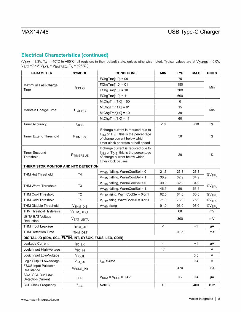
Maximum Fast-Charge Time tFCHG
FChgTmr[1:0] = 00 75
MinFChgTmr[1:0] = 01 150FChgTmr[1:0] = 10 300FChgTmr[1:0] = 11 600
Maintain Charge Time tTOCHG
MtChgTmr[1:0] = 00 0
MinMtChgTmr[1:0] = 01 15MtChgTmr[1:0] = 10 30MtChgTmr[1:0] = 11 60
Timer Accuracy tACC -10 +10 %
Timer Extend Threshold PTIMERX
If charge current is reduced due to ILIM or TDIE, this is the percentage of charge current below which timer clock operates at half speed
50 %
Timer Suspend Threshold PTIMERSUS
If charge current is reduced due to ILIM or TDIE, this is the percentage of charge current below which timer clock pauses
20 %
THERMISTOR MONITOR AND NTC DETECTION
THM Hot Threshold T4VTHM falling, WarmCoolSel = 0 21.3 23.3 25.3
%VTPUVTHM falling, WarmCoolSel = 1 30.9 32.9 34.9
THM Warm Threshold T3VTHM falling, WarmCoolSel = 0 30.9 32.9 34.9
%VTPUVTHM falling, WarmCoolSel = 1 46.5 50 53.5THM Cool Threshold T2 VTHM rising, WarmCoolSel = 0 or 1 62.5 64.5 66.5 %VTPUTHM Cold Threshold T1 VTHM rising, WarmCoolSel = 0 or 1 71.9 73.9 75.9 %VTPUTHM Disable Threshold VTHM_DIS VTHM rising 91.0 93.0 95.0 %VTPUTHM Threshold Hysteresis VTHM_DIS_H 60 mVJEITA BAT Voltage Reduction VBAT_JEITA 300 mV
THM Input Leakage ITHM_LK -1 +1 µATHM Detection Time tTHM_DET 0.35 ms
DIGITAL I/O (SDA, SCL, FLTIN, INT, SYSOK, FSUS, LED, CDIR)Leakage Current IIO_LK -1 +1 µA
Logic Input High-Voltage VIO_IH 1.4 V
Logic Input Low-Voltage VIO_IL 0.5 VLogic Output Low-Voltage VIO_OL IOL = 4mA 0.4 VFSUS Input Pulldown Resistance RFSUS_PD 470 kΩ
SDA, SCL Bus Low-Detection Current IPD VSDA = VSCL = 0.4V 0.2 0.4 µA
SCL Clock Frequency fSCL Note 3 0 400 kHz
MAX14748 USB Type-C Charger
www.maximintegrated.com Maxim Integrated │ 8
Electrical Characteristics (continued)
(VBAT = 8.3V, TA = -40°C to +85°C, all registers in their default state, unless otherwise noted. Typical values are at VCHGIN = 5.0V, VBAT =7.4V, VSYS = VBATREG, TA = +25°C.)
PARAMETER SYMBOL CONDITIONS MIN TYP MAX UNITS
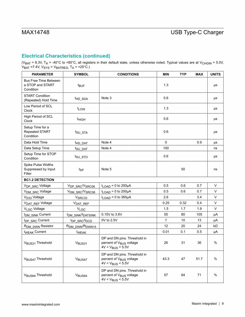
Bus Free Time Between a STOP and START Condition
tBUF 1.3 µs
START Condition (Repeated) Hold Time tHD_SDA Note 3 0.6 µs
Low Period of SCL Clock tLOW 1.3 µs
High Period of SCL Clock tHIGH 0.6 µs
Setup Time for a Repeated START Condition
tSU_STA 0.6 µs
Data Hold Time tHD_DAT Note 4 0 0.9 µsData Setup Time tSU_DAT Note 4 100 ns
Setup Time for STOP Condition tSU_STO 0.6 µs
Spike Pulse Widths Suppressed by Input Filter
tSP Note 5 50 ns
BC1.2 DETECTIONVDP_SRC Voltage VDP_SRC/VSRC06 ILOAD = 0 to 200µA 0.5 0.6 0.7 VVDM_SRC Voltage VDM_SRC/VSRC06 ILOAD = 0 to 200µA 0.5 0.6 0.7 VVD33 Voltage VSRC33 ILOAD = 0 to 365µA 2.6 3.4 VVDAT_REF Voltage VDAT_REF 0.25 0.32 0.4 VVLGC Voltage VLGC 1.5 1.7 1.9 VIDM_SINK Current IDM_SINK/IDATSINK 0.15V to 3.6V 55 80 105 µAIDP_SRC Current IDP_SRC/IDCD 0V to 2.5V 7 10 13 μARDM_DWN Resistor RDM_DWN/RDWN15 12 20 24 kΩIWEAK Current IWEAK 0.01 0.1 0.5 µA
VBUS31 Threshold VBUS31
DP and DN pins. Threshold in percent of VBUS voltage 4V < VBUS < 5.5V
26 31 36 %
VBUS47 Threshold VBUS47
DP and DN pins. Threshold in percent of VBUS voltage 4V < VBUS < 5.5V
43.3 47 51.7 %
VBUS64 Threshold VBUS64
DP and DN pins. Threshold in percent of VBUS voltage 4V < VBUS < 5.5V
57 64 71 %
MAX14748 USB Type-C Charger
www.maximintegrated.com Maxim Integrated │ 9
Electrical Characteristics (continued)
(VBAT = 8.3V, TA = -40°C to +85°C, all registers in their default state, unless otherwise noted. Typical values are at VCHGIN = 5.0V, VBAT =7.4V, VSYS = VBATREG, TA = +25°C.)
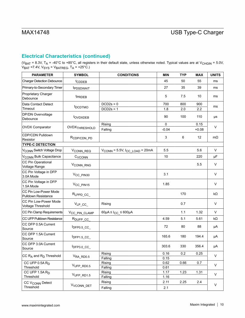
PARAMETER SYMBOL CONDITIONS MIN TYP MAX UNITSCharger Detection Debounce tCDDEB 45 50 55 ms
Primary-to-Secondary Timer tPDSDWAIT 27 35 39 ms
Proprietary Charger Debounce tPRDEB 5 7.5 10 ms
Data Contact Detect Timeout tDCDTMO
DCD2s = 0 700 800 900 msDCD2s = 1 1.8 2.0 2.2
DP/DN Overvoltage Debounce tOVDXDEB 90 100 110 µs
OVDX Comparator OVDXTHRESHOLDRising 0 0.15
VFalling -0.04 +0.08
CDP/CDN Pulldown Resistor RCDP/CDN_PD 3 6 12 mΩ
TYPE-C DETECTIONVCONN Switch Voltage Drop VCONN_REQ VCONN = 5.5V, ICC_LOAD = 20mA 5.5 5.6 V
VCONN Bulk Capacitance CVCONN 10 220 µFCC Pin Operational Voltage Range VCONN_RNG 5.5 V
CC Pin Voltage in DFP 3.0A Mode VCC_PIN30 3.1 V
CC Pin Voltage in DFP 1.5A Mode VCC_PIN15 1.85 V
CC Pin Low-Power Mode Pulldown Resistance RLPPD_CC_ 170 kΩ
CC Pin Low-Power Mode Voltage Threshold VLP_CC_ Rising 0.7 V
CC Pin Clamp Requirements VCC_PIN_CLAMP 60µA ≤ ICC_≤ 600µA 1.1 1.32 V
CC UFP Pulldown Resistance RDUFP_CC_ 4.59 5.1 5.61 kΩCC DFP 0.5A Current Source IDFP0.5_CC_ 72 80 88 µA
CC DFP 1.5A Current Source IDFP1.5_CC_ 165.6 180 194.4 µA
CC DFP 3.0A Current Source IDFP3.0_CC_ 303.6 330 356.4 µA
CC RA and RD Threshold VRA_RD0.5Rising 0.16 0.2 0.25 VFalling 0.15
CC UFP 0.5A RD Threshold VUFP_RD0.5
Rising 0.62 0.66 0.7VFalling 0.61
CC UFP 1.5A RD Threshold VUFP_RD1.5
Rising 1.17 1.23 1.31 VFalling 1.16
CC VCONN Detect Threshold VVCONN_DET
Rising 2.11 2.25 2.4V
Falling 2.1
MAX14748 USB Type-C Charger
www.maximintegrated.com Maxim Integrated │ 10
Electrical Characteristics (continued)
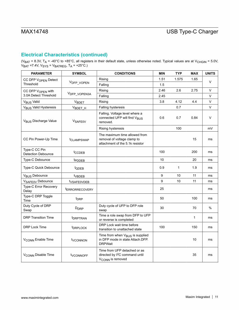
(VBAT = 8.3V, TA = -40°C to +85°C, all registers in their default state, unless otherwise noted. Typical values are at VCHGIN = 5.0V, VBAT =7.4V, VSYS = VBATREG, TA = +25°C.)
PARAMETER SYMBOL CONDITIONS MIN TYP MAX UNITS
CC DFP VOPEN Detect Threshold VDFP_VOPEN
Rising 1.51 1.575 1.65V
Falling 1.5
CC DFP VOPEN with 3.0A Detect Threshold VDFP_VOPEN3A
Rising 2.46 2.6 2.75 VFalling 2.45 V
VBUS Valid VBDET Rising 3.8 4.12 4.4 VVBUS Valid Hysteresis VBDET_H Falling hysteresis 0.7 V
VBUS Discharge Value VSAFE0V
Falling. Voltage level where a connected UFP will find VBUS removed.
0.6 0.7 0.84 V
Rising hysteresis 100 mV
CC Pin Power-Up Time tCLAMPSWAP
The maximum time allowed from removal of voltage clamp to attachment of the 5.1k resistor
15 ms
Type-C CC Pin Detection Debounce tCCDEB 100 200 ms
Type-C Debounce tPDDEB 10 20 ms
Type-C Quick Debounce tQDEB 0.9 1 1.9 ms
VBUS Debounce tVBDEB 9 10 11 msVSAFE0V Debounce tVSAFE0VDEB 9 10 11 msType-C Error Recovery Delay tERRORRECOVERY 25 ms
Type-C DRP Toggle Time tDRP 50 100 ms
Duty Cycle of DRP Swap DDRP
Duty cycle of UFP to DFP role swap 30 70 %
DRP Transition Time tDRPTRANTime a role swap from DFP to UFP or reverse is completed 1 ms
DRP Lock Time tDRPLOCKDRP Lock wait time before transition to unattached state 100 150 ms
VCONN Enable Time tVCONNON
Time from when VBUS is supplied in DFP mode in state Attach.DFP.DRPWait
10 ms
VCONN Disable Time tVCONNOFF
Time from UFP detached or as directed by I2C command until VCONN is removed
35 ms
MAX14748 USB Type-C Charger
www.maximintegrated.com Maxim Integrated │ 11
Electrical Characteristics (continued)
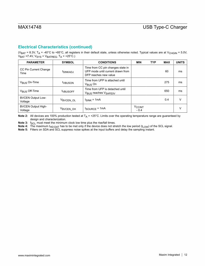
(VBAT = 8.3V, TA = -40°C to +85°C, all registers in their default state, unless otherwise noted. Typical values are at VCHGIN = 5.0V, VBAT =7.4V, VSYS = VBATREG, TA = +25°C.)
Note 2: All devices are 100% production tested at TA = +25°C. Limits over the operating temperature range are guaranteed by design and characterization.
Note 3: fSCL must meet the minimum clock low time plus the rise/fall times.Note 4: The maximum tHD:DAT has to be met only if the device does not stretch the low period (tLOW) of the SCL signal.Note 5: Filters on SDA and SCL suppress noise spikes at the input buffers and delay the sampling instant.
PARAMETER SYMBOL CONDITIONS MIN TYP MAX UNITS
CC Pin Current Change Time tSINKADJ
Time from CC pin changes state in UFP mode until current drawn from DFP reaches new value
60 ms
VBUS On-Time tVBUSON Time from UFP is attached until VBUS On 275 ms
VBUS Off-Time tVBUSOFFTime from UFP is detached until VBUS reaches VSAFE0V
650 ms
BVCEN Output Low-Voltage VBVCEN_OL ISINK = 1mA 0.4 V
BVCEN Output High-Voltage VBVCEN_OH ISOURCE = 1mA VCCINT
- 0.4 V
MAX14748 USB Type-C Charger
www.maximintegrated.com Maxim Integrated │ 12
Electrical Characteristics (continued)
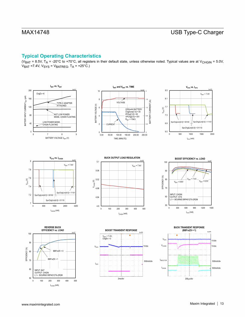
(VBAT = 8.5V, TA = -20°C to +70°C, all registers in their default state, unless otherwise noted. Typical values are at VCHGIN = 5.0V, VBAT =7.4V, VSYS = VBATREG, TA = +25°C.)
7
7.2
7.4
7.6
7.8
8
0 800 1600 2400 3200
V SYS
(V)
ICHGIN (mA)
VSYS vs. ICHGINtoc04
VBAT = 7.4V
SpvChgILim[4:0] = 11101
SpvChgILim[4:0] = 01110
SpvChgILim[4:0] = 00100
4.9
4.94
4.98
5.02
5.06
5.1
0 100 200 300 400 500
V CH
GIN
(V)
ICHGIN (mA)
BUCK OUTPUT LOAD REGULATIONtoc05
VBAT = 7.4V
50
60
70
80
90
100
0 300 600 900 1200 1500
EFFI
CIE
NC
Y (%
)
ISYS (mA)
BOOST EFFICIENCY vs. LOADtoc06
VBAT = 6.0VVBAT = 8.6VVBAT = 7.4V
INPUT: CHGINOUTPUT: SYSL1 = BOURNS SRP4012TA-2R2M
0
40
80
120
160
200
6 7 8 9
BATT
ERY
INPU
T C
UR
REN
T I B
AT(µ
A)
BATTERY VOLTAGE VBAT (V)
IBAT vs. VBAT
toc01
LOW POWER MODE,CHGIN FLOATING
TYPE-C ADAPTER ATTACHED
NOT LOW POWER MODE, CHGIN FLOATING
ChgEn =0
0
0.4
0.8
1.2
1.6
2
0
2
4
6
8
10
0.00 50.00 100.00 150.00 200.00 250.00
BATT
ERY
CU
RR
ENT
(A)
BATT
ERY
VOLT
AGE
(V)
TIME (MINUTE)
IBAT and VBAT vs. TIMEtoc02
2200mAH BATTERYChgDone[1:0] = 00IPChg[1:0] = 00VPChg[2:0] = 001RSET = 10kW
VOLTAGE
CURRENT
6.5
6.9
7.3
7.7
8.1
8.5
0 500 1000 1500 2000
V SYS
(V)
ISYS (mA)
VSYS vs. ISYStoc03
VBAT = 7.4V
SpvChgILim[4:0] = 11101
SpvChgILim[4:0] = 01110
SpvChgILim[4:0] = 00100
50
60
70
80
90
100
0 100 200 300 400 500
EFFI
CIE
NC
Y (%
)
ICHGIN (mA)
REVERSE BUCK EFFICIENCY vs. LOAD
toc07
BBFrxZX = 0
INPUT: BATOUTPUT: CHGINL1 = BOURNS SRP4012TA-2R2M
BBFrxZX = 1
toc08
2ms/div
BOOST TRANSIENT RESPONSE
VSYS1V/div
ISYS
500mA/div
VBAT = 7.4V, ChgEn = 0
500mA/div
toc09
200ms/div
BUCK TRANSIENT RESPONSE(BBFrxZX = 1)
VSYS
1V/div
ICHGIN
VCHGIN
IINDUCTOR 500mA/div
1V/div
MAX14748 USB Type-C Charger
Maxim Integrated │ 13www.maximintegrated.com
Typical Operating Characteristics
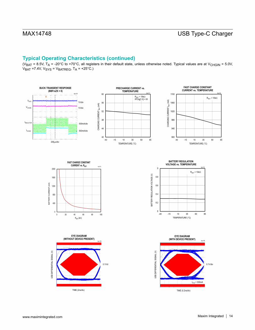
(VBAT = 8.5V, TA = -20°C to +70°C, all registers in their default state, unless otherwise noted. Typical values are at VCHGIN = 5.0V, VBAT =7.4V, VSYS = VBATREG, TA = +25°C.)
0
400
800
1200
1600
2000
0 20 40 60 80 100
BA
TT
ER
Y C
UR
RE
NT
(m
A)
RSET (kW)
FAST CHARGE CONSTANT CURRENT vs. RSET toc13
500mA/div
toc10
200ms/div
BUCK TRANSIENT RESPONSE(BBFrxZX = 0)
VSYS
1V/div
ICHGIN
VCHGIN
IINDUCTOR 500mA/div
1V/div
toc16
TIME (0.2ns/div)
EYE DIAGRAM(WITH DEVICE PRESENT)
USB
DIF
FER
ENTI
AL S
IGN
AL (V
)
0.1V/div
VL3OUT = 3.0V
ISYS = 300mA
40
44
48
52
56
60
-40 -15 10 35 60 85
CH
ARG
ING
CU
RR
ENT
I BAT
(mA)
TEMPERATURE (°C)
PRECHARGE CURRENT vs.TEMPERATURE
toc11
RSET = 10kWIPChg[1:0] = 00
900
940
980
1020
1060
1100
-40 -15 10 35 60 85
CH
ARG
ING
CU
RR
ENT
I BAT
(mA)
TEMPERATURE (°C)
FAST CHARGE CONSTANTCURRENT vs. TEMPERATURE
toc12
RSET = 10kW
8
8.2
8.4
8.6
8.8
9
-40 -15 10 35 60 85
BATT
ERY
REG
ULA
TIO
N V
OLT
AGE
(V)
TEMPERATURE (°C)
BATTERY REGULATION VOLTAGE vs. TEMPERATURE
toc14
RSET = 10kW
toc15
TIME (2ns/div)
EYE DIAGRAM(WITHOUT DEVICE PRESENT)
USB
DIF
FER
ENTI
AL S
IGN
AL (V
)
0.1V/div
MAX14748 USB Type-C Charger
Maxim Integrated │ 14www.maximintegrated.com
Typical Operating Characteristics (continued)
1 2 3 4
A
B
C
D GND
THM
VTPU
GND
BREGFSUS
E
5
SYSOK
NVP
SDA
LED
AGND
CC1
SCL
CC2
CDN
6
FLTIN COMP
CHGIN
GND
F
CDIR
CDP TDP CHGIN
INT
VCONN BST
TPU
DGND
TDN
SYS
SET
BYP
PGND
LX
SYS
BAT
BYP
PGND
LX
7
CHGINCHGIN
SYS
BAT
BYP
PGND
LX
SYS
BAT
BYP
PGND
LX
8 9
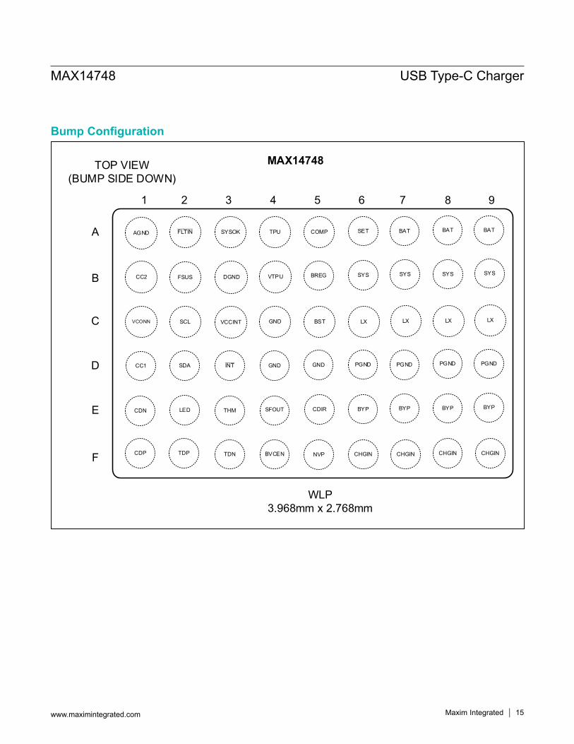
TOP VIEW (BUMP SIDE DOWN)
MAX14748
WLP3.968mm x 2.768mm
VCCINT
SFOUT
BVCEN
MAX14748 USB Type-C Charger
www.maximintegrated.com Maxim Integrated │ 15
Bump Configuration
BUMP NAME FUNCTIONA1 AGND Analog Ground.
A2 FLTIN Charger Fault Input. Logic-low on this pin forces the charger into a fault state and generates an interrupt. See Register 0x35 description for more information. Connect to digital I/O supply if not used.
A3 SYSOKOpen-Drain Status Output of SYS Regulation. When VSYS is above the SYS UVLO threshold and Boost is active, this output is high-impedance. When VSYS is below the SYS UVLO threshold, this output is low. Leave unconnected if not used.
A4 TPU High-Side of Internal Resistor for THM Detection. Connect a 10k resistor between this pin and THM.
A5 COMP Buck/Boost Converter Compensation Connection. Connect a 3.9nF capacitor for internal Buck/Boost compensation
A6 SETExternal Resistor Connection for Fast Charge Current Setting. Connect a resistor to this pin to set the fast charge current. Other charge currents are set as a proportion of fast charge current based on I2C register settings.
A7–A9 BATBattery Connection. Connect a 2s Li-ion+ battery from BAT to GND. Bypass to PGND with a parallel combination of a 0.1µF capacitor and an effective 10µF - 30µF capacitor. Keep the capacitors as close to BAT as possible and keep the stray inductance and resistance of the trace from BAT to the battery terminal as low as possible.
B1 CC2 USB Type-C CC2. Connect to CC2 on USB Type-C connector.
B2 FSUS Force Suspend Input. Logic-high on this pin causes the input limiter to open and input current from CHGIN is reduced to zero. This pin is internally pulled to GND through a 470kΩ (typ) resistor and has no effect if FSUSMsk = 1.
B3 DGND Digital Ground.B4 VTPU External Voltage Input for TPU connection. Connect to external supply or VCCINT.B5 BREG Bypass for Internal Switching Converter Supply. Bypass with 1µF capacitor to AGND.
B6–B9 SYS System Load Connection. Connect SYS to the system load. Bypass to PGND with a parallel combination of a 0.1µF capacitor and an effective 22µF capacitor. (Note: there is a diode between SYS and BAT)
C1 VCONN External VCONN Supply Input. Leave unconnected if not used.C2 SCL I2C Serial Clock Input. Connect an external pull-up resistor.C3 VCCINT Bypass For Internal Analog Supply. Bypass with 1µF capacitor to GND.
C4, D4, D5 GND Ground.
C5 BST Charge Pump Connection. Connect a 0.1µF capacitor between BST and LX.
C6, C7, C8, C9 LX Switching Node of Boost Converter. Connect a 1.5µH or 2.2µH inductor between LX and BYP. See
Applications Information section for more details.
D1 CC1 USB Type-C CC1. Connect to CC1 on USB Type-C connector.D2 SDA I2C Serial Data Input/Output. Connect an external pullup resistor.D3 INT Active-Low, Open-Drain Interrupt Output. Connect an external pullup resistor.
D6, D7, D8, D9 PGND Power Ground.
MAX14748 USB Type-C Charger
www.maximintegrated.com Maxim Integrated │ 16
Bump Descriptions
Note: All capacitance values listed in this document refer to effective capacitance. Be sure to specify capacitors that will meet these requirements under typical system operating conditions taking into consideration the effects of voltage and temperature.
BUMP NAME FUNCTIONE1 CDN USB Connector D-Input. Leave unconnected if not used.
E2 LED
LED Charging Status Indicator. Open-drain output indicating battery charging status. When LEDAuto = 1 and a temperature fault is detected, the output is pulsed at 50% duty cycle for a period of 1.5s. When a charge timer expires or SysFlt fault occurs, LED is pulsed at 50% for a period of 0.15s. When LEDAuto = 0, the open-drain output is controlled by the LEDCtrl bit. Connect this pin to GND if unused.
E3 THM Battery Temperature Thermistor Measurement Connection. This pin is used for NTC thermistor presence detection and JEITA compliant temperature control.
E4 SFOUT Output of overvoltage protected LDO powered from CHGIN. Bypass SFOUT with a 1µF ceramic capacitor to GND.
E5 CDIR USB Cable Orientation Open-drain Output. When CC1 is active, this output is pulled low. Otherwise, this output is high-impedance. Leave unconnected if not used.
E6–E9 BYP Bypass Connection. Bypass to PGND with a parallel combination of a 0.1µF capacitor and an effective 10µF capacitor.
F1 CDP USB Connector D+ Input. Leave unconnected if not used.
F2 TDP USB Transceiver D+ Connection. Connect TDP to device microprocessor USB transceiver D+ line. Leave unconnected if not used.
F3 TDN USB Transceiver D- Connection. Connect TDN to device microprocessor USB transceiver D- line. Leave unconnected if not used.
F4 BVCEN External VCONN Supply Enable Output. Push-pull output between VCCINT and GND. Leave unconnected if not used.
F5 NVP Negative Voltage PFET Gate Control. Leave unconnected if not used.
F6–F9 CHGIN USB Charger Input. Bypass this pin with a 1µF capacitor to PGND.
MAX14748 USB Type-C Charger
www.maximintegrated.com Maxim Integrated │ 17
Bump Descriptions (continued)
MAX14748 USB Type-C Charger
www.maximintegrated.com Maxim Integrated │ 18
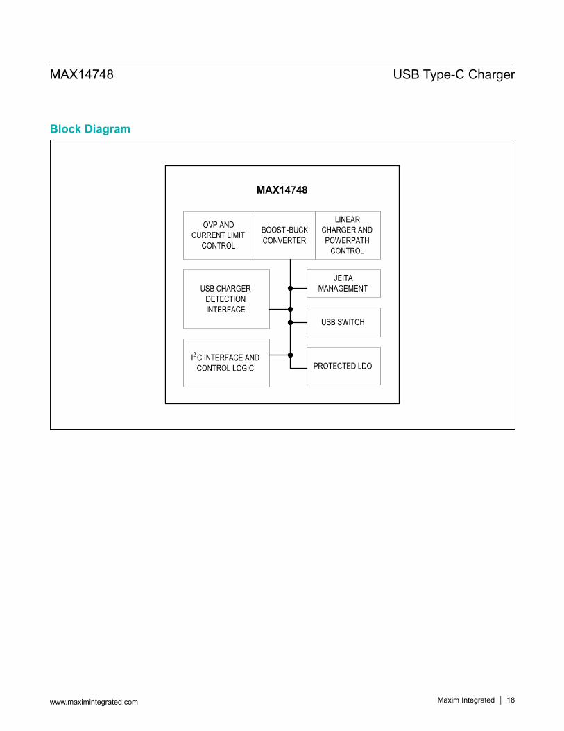
Block Diagram
Detailed DescriptionThe MAX14748 is a battery charger with a Smart Power Selector that safely charges two Li+ cell in accordance with JEITA specifications*.
Input OVPThe MAX14748 CHGIN input is protected by an internal N-channel FET. The device monitors the voltage at CHGIN and, if CHGIN is greater than VOVP, switches off the internal FET to prevent damage to the device. If VCHGIN is above the overvoltage threshold or below the USB valid voltage threshold, the MAX14748 enters overvoltage lockout (OVLO). During OVLO, the internal circuits remain powered, the SYSOK pin is high-impedance, and an interrupt is asserted. During OVLO, the charger turns off and the system load switch closes, allowing the battery to power SYS.
Negative Voltage Protection (NVP)The MAX14748 provides a gate protection circuit for an external PFET that protects against negative voltages on VBUS. NVP pin drives the gate of the external PFET. If a negative voltage is present on VBUS, e.g., by a backwards connector, the NVP turns off the external PFET, therefore providing negative voltage protection.
Low Power ModeThe MAX14748 features a Low Power mode, which reduces the battery current consumption from 25µA to 140µA. To enter Low Power mode, write 1 to LowPowEn (Register 0x33[7]). To manually exit Low Power mode, set LowPowAbort (Register 0x33[1]) to 1. If a DFP pullup connect to CC1/CC2 is detected, the device automatically exits Low Power mode and resumes normal operations.
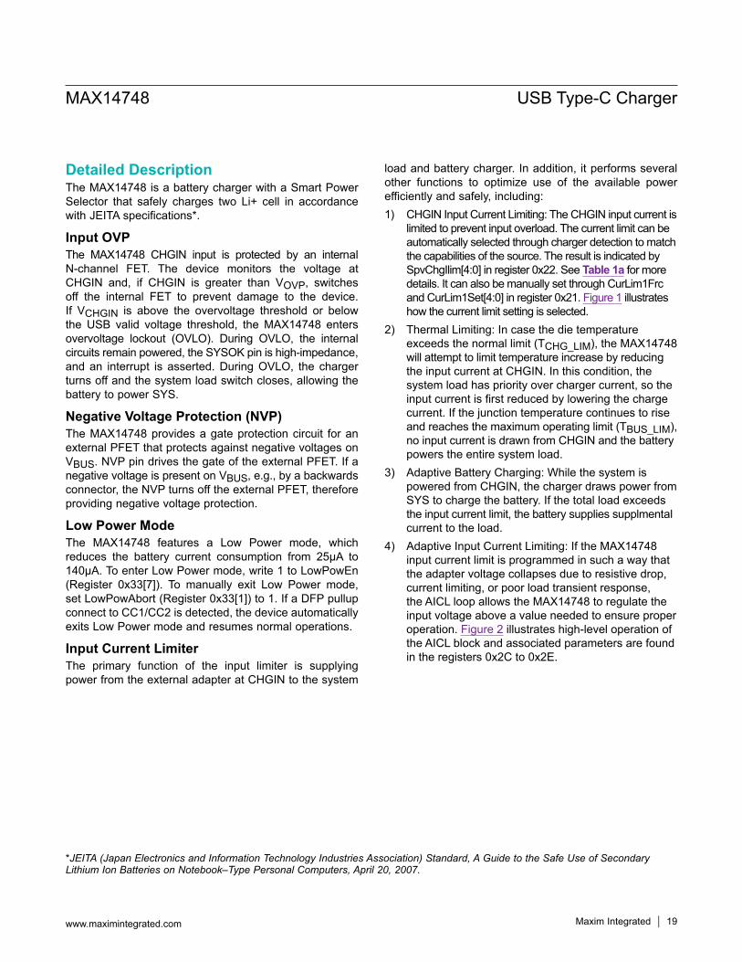
Input Current LimiterThe primary function of the input limiter is supplying power from the external adapter at CHGIN to the system
load and battery charger. In addition, it performs several other functions to optimize use of the available power efficiently and safely, including:1) CHGIN Input Current Limiting: The CHGIN input current is
limited to prevent input overload. The current limit can be automatically selected through charger detection to match the capabilities of the source. The result is indicated by SpvChgIlim[4:0] in register 0x22. See Table 1a for more details. It can also be manually set through CurLim1Frc and CurLim1Set[4:0] in register 0x21. Figure 1 illustrates how the current limit setting is selected.
2) Thermal Limiting: In case the die temperature exceeds the normal limit (TCHG_LIM), the MAX14748 will attempt to limit temperature increase by reducing the input current at CHGIN. In this condition, the system load has priority over charger current, so the input current is first reduced by lowering the charge current. If the junction temperature continues to rise and reaches the maximum operating limit (TBUS_LIM), no input current is drawn from CHGIN and the battery powers the entire system load.
3) Adaptive Battery Charging: While the system is powered from CHGIN, the charger draws power from SYS to charge the battery. If the total load exceeds the input current limit, the battery supplies supplmental current to the load.
4) Adaptive Input Current Limiting: If the MAX14748 input current limit is programmed in such a way that the adapter voltage collapses due to resistive drop, current limiting, or poor load transient response, the AICL loop allows the MAX14748 to regulate the input voltage above a value needed to ensure proper operation. Figure 2 illustrates high-level operation of the AICL block and associated parameters are found in the registers 0x2C to 0x2E.
*JEITA (Japan Electronics and Information Technology Industries Association) Standard, A Guide to the Safe Use of Secondary Lithium Ion Batteries on Notebook–Type Personal Computers, April 20, 2007.
MAX14748 USB Type-C Charger
www.maximintegrated.com Maxim Integrated │ 19
Table 1a. Automatic Input Current Limit ControlChgTyp[1:0] PrChgTyp[2:0] CCIStat[1:0] SDPMaxCur[1:0] CDPMaxCur[1:0] ILIM SpvChgIlim[4:0]
“xx” “xxx” “11 = 3A” “00” “0” 3A 0x1D“11 = 1.5A” “xxx” “11 = 3A” “xx” “x” 3A 0x1D
“xx” “110 = 3A” “xx” “xx” “x” 3A 0x1D
“xx” “101 = 2.4A”“00” or
“01 = 500mA” or “10 = 1.5A”
“xx” “x” 2.4A 0x17
“xx” “100 = 2A” or “001 = 2A”
“00” or “01 = 500mA” or
“10 = 1.5A”“xx” “x” 2A 0x13
“1x = 1.5A” “000” or “010 = 500mA”
“00” or “01 = 500mA” or
“10 = 1.5A”“xx” “x” 1.5A 0x0E
“1x = 1.5A”“000” or
“010 = 500mA” or “011 = 1A”
“10 = 1.5A” “xx” “x” 1.5A 0x0E
“xx” “011 = 1A” “00” or “01 = 500mA” “xx” “x” 1A 0x09
“01 = 500mA” “000” or “010 = 500mA”
“00” or “01 = 500mA” “xx” “x” 0.5A 0x04
“01 = 500mA” “000” “10 = 1.5A” or “11 = 3A” 01 “x” 0.5A 0x04
“01 = 500mA” “000” “10 = 1.5A” or “11 = 3A” 10 “X” 1.0A 0x09
“01 = 500mA” “000” “10 = 1.5A” or “11 = 3A” 11 “x” 1.5A 0x0E
“10 = 1.5A” “000” “11 = 3A” xx “1” 1.5A 0x0E“00” “xxx” “xx” “xx” “x” NA NA
MAX14748 USB Type-C Charger
www.maximintegrated.com Maxim Integrated │ 20
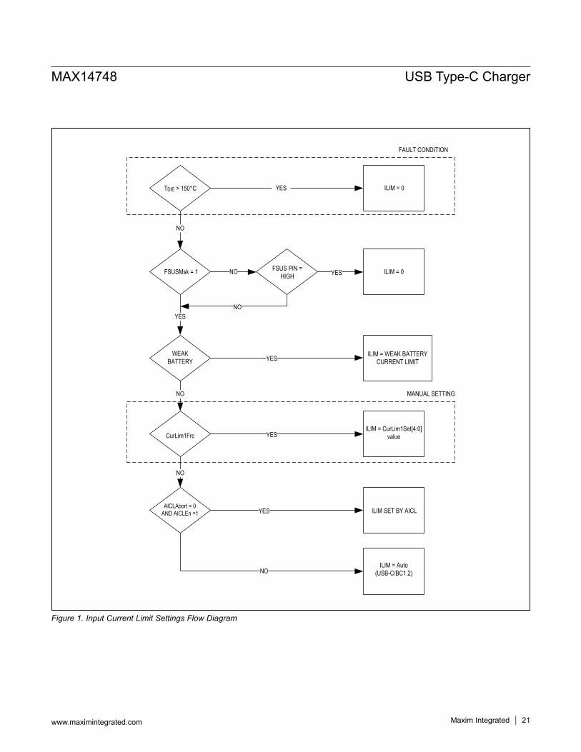
Figure 1. Input Current Limit Settings Flow Diagram
NO
NO
NO
YES
YES
TDIE > 150°C ILIM = 0
ILIM = 0
ILIM = WEAK BATTERY CURRENT LIMIT
FSUS PIN = HIGH
FSUSMsk = 1
WEAK BATTERY YES
YES
YES
NO
CurLim1FrcILIM = CurLim1Set[4:0]
value
AICLAbort = 0 AND AICLEn =1 ILIM SET BY AICL
ILIM = Auto(USB-C/BC1.2)
NO
NO
FAULT CONDITION
MANUAL SETTING
YES
MAX14748 USB Type-C Charger
www.maximintegrated.com Maxim Integrated │ 21
Figure 2. AICL Operation Flow Diagram
AICL INCREMENTINPUT CURRENT = MIN
(STOP CURRENT, INPUT CURRENT + 100mA)
AICL PRECHECKSTOP CURRENT = AICLMaxI[4:0]
INPUT CURRENT = PREVIOUS SETTING
AICL IDLEINPUT CURRENT = STOP CURRENT
AICL BLANKINPUT CURRENT = 0,
STOP CURRENT = INPUT CURRENT – 100mAVBDET MASKED AND OVP CLOSED
AICLAbort = 0 ANDAICLEn = 1
VBYP < VBYPUVLO
AND TBLANK TIMEOUT
VBYP > VBYPUVLO AND
VCHGIN > VBDET
VBYP < VBYPUVLO
AICL OFFSTOP CURRENT = 500mAMIN CURRENT = 100mA
INPUT CURRENT = PREVIOUS SETTING
AICL INITINPUT CURRENT = MIN CURRENT
VBYP > VBYPUVLO AND INPUT CURRENT = STOP CURRENT
VBYP < VBYPUVLO
TSTEP TIMEOUT
AICLAbort = 1
AICLEn = 1
AICL NO CONNECTIONINPUT CURRENT = PREVIOUS SETTING
STOP CURRENT = 500mA
ChgStat[3:0] ≠ 0011
MAX14748 USB Type-C Charger
www.maximintegrated.com Maxim Integrated │ 22
Boost Converter with Reverse Buck Boost ModeThe MAX14748 boost converter operates as either a current-limited voltage source, or current source, depending on the charger operational state. When a valid USB voltage is present at CHGIN, and the charger is disabled, VSYS is regulated to VBAT + 400mV. If the charger is in precharge mode, VSYS is regulated to VPCHG + 400mV. When the system is in fast-charge mode, the boost converter operates as a current source, delivering current into the SYS node that is shared by the battery and system loads.The boost converter current limit may be acted upon by multiple system blocks, including the programmed input current limit, thermal status, charging current, SYS regulation voltage block, and battery termination voltage block. The minimum requested current from these blocks at any given time determines the active current limit in the boost.
Reverse Buck ModeThe CHGIN-SYS switching converter may operate as a buck converter when needed to supply a load attached to CHGIN. The load may be a Type-C sink or some other proprietary device. If Type-C DRP operation is enabled, the buck converter can be enabled by the Type-C state machine. The output voltage of the buck can be programmed from 4V to 5.5V in 0.1V steps by writing to BuckVSet[3:0], however, it is not recommended to change the output voltage when the buck is active.
The output of the buck converter turns off when a fault occurs. The specific fault occurred is indicated by DCDCILim, DCDCRunAway, DCDCPGood status bits (register 0x04). See Register Descriptions for more details. When the buck is disabled due to a fault, both VBUSDet (register 0x07) and VSAFE0V (register 0x0A) change to 0. After the fault condition is removed, the buck converter can be restarted by writing 1 to CCSnkRst, CCSrcRst, CCForceError, or USBCRset auto-reset bits.
Smart Power SelectorThe Smart Power Selector seamlessly distributes power between CHGIN, battery (BAT) and the system (SYS). The basic modes of operation of the smart power selec-tor are:1. With a valid external power source:
a. The external power source at CHGIN is the primary source of energy.
b. The battery is the secondary source of energy.c. Energy delivery to SYS is the highest priority.d. Any energy that is not required by SYS is available
to the battery.2. With no power source available at CHGIN:
a. The battery is the primary source of energy.b. Energy delivery to SYS has the highest priority.
3. With a Type-C Sink or other load present at CHGIN: a. The battery is the primary source of energy.b. Energy delivery to SYS is the highest priority.c. Energy delivery to BYP is the second highest
priority.
MAX14748 USB Type-C Charger
www.maximintegrated.com Maxim Integrated │ 23
4. SYS Regulation Voltage: a. When the charger path is enabled and the
charger is disabled, VSYS is regulated to VBAT + 400mV and BAT switch is off.
b. When the charger is enabled but in a non-charging state such as maitain charge done, thermistor suspend, or timer fault, VSYS is regulated to VBAT + 400mV and BAT switch is off.
c. When the input charger path is enabled and the battery is charging in prequalification, VSYS is regulated to VPCHG + 400mV. Charge current is reduced when VSYS approaches VPCHG + 200mV.
d. When the input charger path is enabled and the battery is charging in fast-charge or maintain charge done, the BAT switch is closed and VSYS = VBAT. In maintain charge done state, the connection between SYS and BAT acts as an ideal diode. Therefore, when VSYS drops below VBAT, the BAT switch is turned fully on and the battery supplements the SYS load along with the current from CHGIN.
e. When the switching converter is enabled as a reverse buck, the BAT switch is closed and VSYS = VBAT.
Short-Circuit ProtectionThe MAX14748 provides short-circuit protection to the power nodes. When SYS is shorted to ground, input current from CHGIN is limited by boost converter current limit. Note in this case, FET diode from BAT-SYS prevents control of FET BAT-SYS current. Battery current is not limited by the MAX14748 and a pack protector is needed to limit the battery current.
When either BYP or CHGIN is shorted to ground, the current from BAT is limited by the reverse buck converter.
USB Type-C 1.1USB Type-C 1.1 UFP and DRP SupportThe MAX14748 provides support for devices functioning as a Upstream Facing Port (UFP) or Dual Role Port (DRP) per the current USB Type-C 1.1 specification. When acting as a power source in DRP mode, the MAX14748 can provide a 5V VBUS on the CHGIN pin through operation of the reverse buck converter. The USB Type-C VCONN supply is provided externally via the VCONN pin, and switched internally onto one of the CC pins. An open-drain output pin, BVCEN, is provided to enable the external VCONN supply based on the Type-C state machine output. BVCEN is a push-pull output between GND and VCCINT.
USB BC1.2 Compliant and Nonstandard Charger SupportThe BC1.2 charger detection and special charger detection routine is embedded within the Type-C state machine. The BC1.2 and Special Charger detection routine runs always when the state machine enters the ‘AttachWait.SNK’ state of the USB Type-C 1.1 state-machine.
USB Type-C Adapter InsertionFigure 3a and Figure 3b depict the general timings when a USB Type-C adapter is attached. For more information on the behavior and timings of the USB Type-C 1.1 state-machine, please refer to the USB Type-C specification.
MAX14748 USB Type-C Charger
www.maximintegrated.com Maxim Integrated │ 24
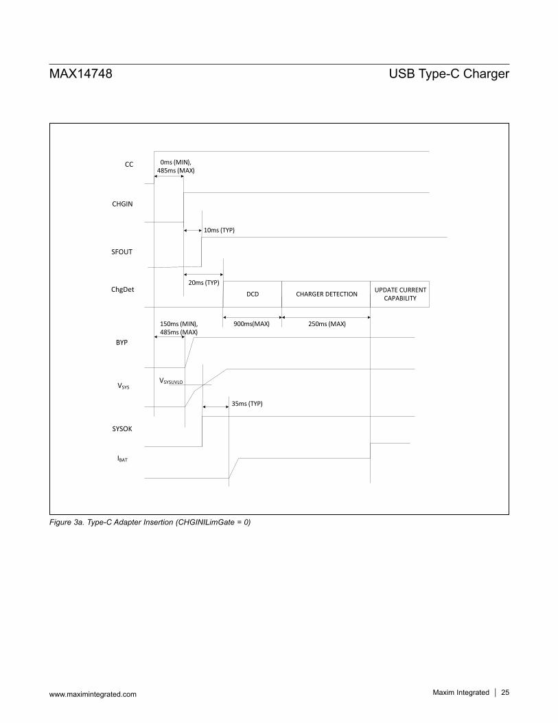
Figure 3a. Type-C Adapter Insertion (CHGINILimGate = 0)
BYP
VSYS
SYSOK
IBAT
35ms (TYP)
CHGIN
CC 0ms (MIN),485ms (MAX)
DCD CHARGER DETECTION UPDATE CURRENTCAPABILITY
10ms (TYP)
900ms(MAX) 250ms (MAX)150ms (MIN),485ms (MAX)
ChgDet
SFOUT
20ms (TYP)
VSYSUVLO
MAX14748 USB Type-C Charger
www.maximintegrated.com Maxim Integrated │ 25
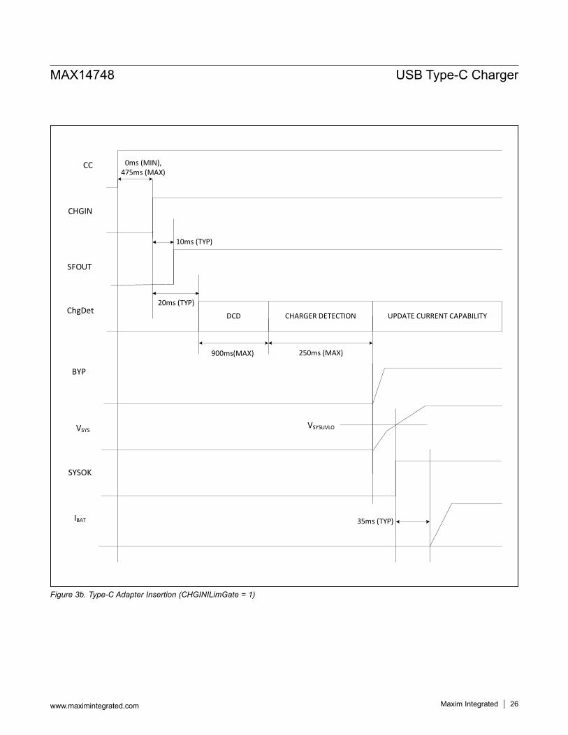
Figure 3b. Type-C Adapter Insertion (CHGINILimGate = 1)
BYP
VSYS
SYSOK
IBAT
CHGIN
CC 0ms (MIN),475ms (MAX)
DCD CHARGER DETECTION UPDATE CURRENT CAPABILITY
10ms (TYP)
900ms(MAX) 250ms (MAX)
ChgDet
SFOUT
20ms (TYP)
VSYSUVLO
35ms (TYP)
MAX14748 USB Type-C Charger
www.maximintegrated.com Maxim Integrated │ 26
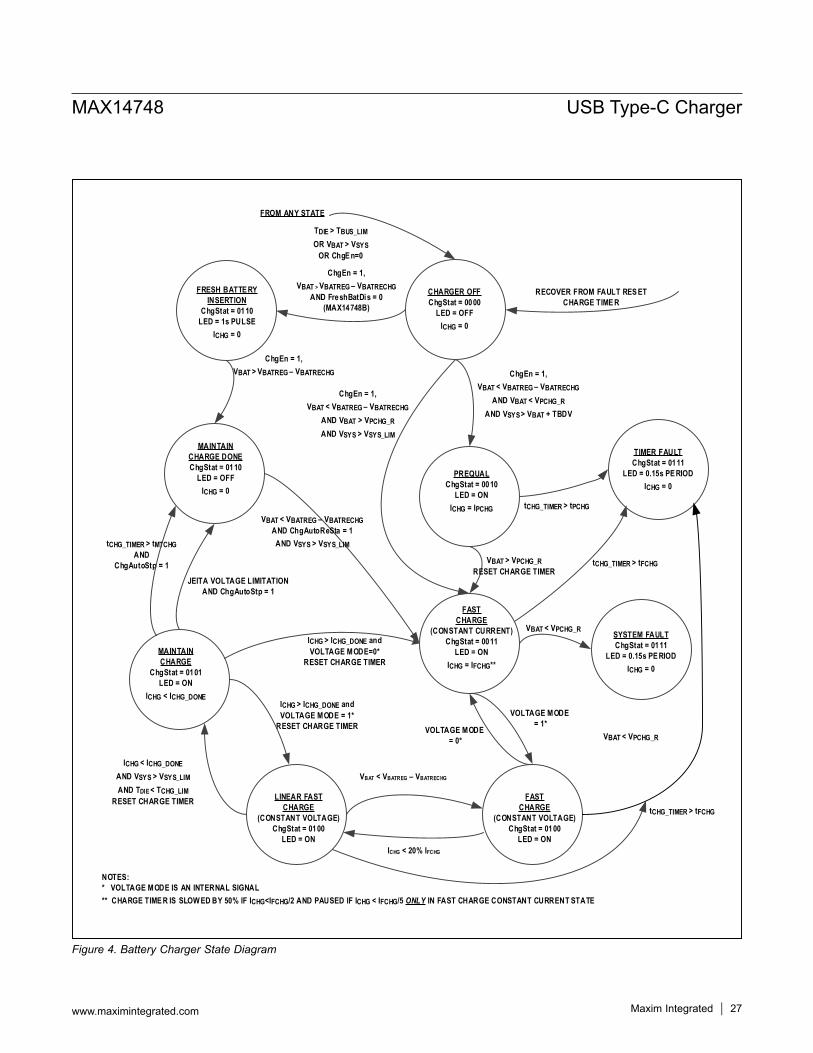
Figure 4. Battery Charger State Diagram
MAINTAINCHARGE DONEChgStat = 0110
LED = OFFICHG = 0
CHARGER OFFChgStat = 0000
LED = OFFICHG = 0
PREQUALChgStat = 0010
LED = ONICHG = IPCHG
FAST CHARGE
(CONSTANT CURRENT)ChgStat = 0011
LED = ONICHG = IFCHG**
FAST CHARGE
(CONSTANT VOLTAGE)ChgStat = 0100
LED = ON
MAINTAINCHARGE
ChgStat = 0101LED = ON
ICHG < ICHG_DONE
FRESH BATTE RY INSERTION
ChgStat = 0110LED = 1s PULSE
ICHG = 0
TIMER FAULTChgStat = 0111
LED = 0.15s PE RIODICHG = 0
ChgEn = 1,VBAT < VBATREG – VBATRECHG
AND VBAT < VPCHG_RAND VSYS > VBAT + TBDV
VBAT > VPCHG_RRESET CHARGE TIMER
VBAT < VPCHG_R
VOLTAGE MODE = 1*
VOLTAGE MODE = 0*
RECOVER FROM FAULT RES ET CHARGE TIME R
ChgEn = 1,VBAT > VBATREG – VBATRECHG
ChgEn = 1, VBAT > VBATREG – VBATRECHG
AND FreshBatDis = 0 (MAX14748B)
ICHG > ICHG_DONE andVOLTAGE MODE = 1*
RESET CHARGE TIMER
ICHG < ICHG_DONE AND VSYS > VSYS_LIMAND TDIE < TCHG_LIM
RESET CHARGE TIMER
ICHG > ICHG_DONE andVOLTAGE MODE=0*
RESET CHARGE TIMER
tCHG_TIMER > tMTCHGAND
ChgAutoStp = 1
VBAT < VBATREG – VBATRECHGAND ChgAutoReSta = 1AND VSYS > VSYS_LIM
tCHG_TIMER > tPCHG
tCHG_TIMER > tFCHG
TDIE > TBUS_LIMOR VBAT > VSYS
OR ChgE n=0
FROM ANY STATE
NOTES:* VOLTAGE MODE IS AN INTERNAL SIGNAL** CHARGE TIME R IS SLOW ED BY 50% IF ICHG<IFCHG/2 AND PAUSED IF ICHG < IFCHG/5 ONLY IN FAST CHARGE CONSTANT CURRENT STATE
SYSTEM FAULTChgStat = 0111
LED = 0.15s PE RIODICHG = 0
JEITA VOLTAGE LIMITATIONAND ChgAutoStp = 1
VBAT < VPCHG_R
ChgEn = 1,VBAT < VBATREG – VBATRECHG
AND VBAT > VPCHG_RAND VSYS > VSYS_LIM
tCHG_TIMER > tFCHG
LINEAR FAST CHARGE
(CONSTANT VOLTAGE)ChgStat = 0100
LED = ONICHG < 20% IFCHG
VBAT < VBATREG – VBATRECHG
MAX14748 USB Type-C Charger
www.maximintegrated.com Maxim Integrated │ 27
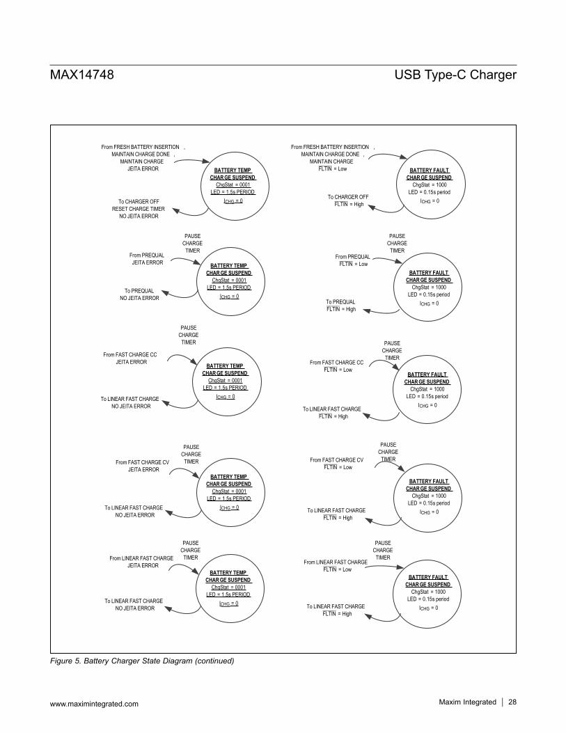
Figure 5. Battery Charger State Diagram (continued)
PAUSECHARGE
TIMER
PAUSECHARGE
TIMER
PAUSECHARGE
TIMER
From PREQUALJEITA ERROR
To PREQUALNO JEITA ERROR
From FAST CHARGE CCJEITA ERROR
From FAST CHARGE CVJEITA ERROR
From FRESH BATTERY INSERTION ,MAINTAIN CHARGE DONE ,
MAINTAIN CHARGEJEITA ERROR
To CHARGER OFFRESET CHARGE TIMER
NO JEITA ERROR
From PREQUALFLTIN = Low
To PREQUALFLTIN = High
From FAST CHARGE CCFLTIN = Low
From FAST CHARGE CVFLTIN = Low
To LINEAR FAST CHARGEFLTIN = High
To CHARGER OFFFLTIN = High
BATTERY FAULTCHAR GE SUSPEND
ChgStat = 1000LED = 0.15s period
ICHG = 0
From FRESH BATTERY INSERTION ,MAINTAIN CHARGE DONE ,
MAINTAIN CHARGEFLTIN = LowBATTERY TEMP
CHAR GE SUSPENDChgStat = 0001
LED = 1.5s PERIOD
ICHG = 0
PAUSECHARGE
TIMER
PAUSECHARGE
TIMER
PAUSECHARGE
TIMER
BATTERY TEMPCHAR GE SUSPEND
ChgStat = 0001LED = 1.5s PERIOD
ICHG = 0
BATTERY TEMPCHAR GE SUSPEND
ChgStat = 0001LED = 1.5s PERIOD
ICHG = 0
BATTERY TEMPCHAR GE SUSPEND
ChgStat = 0001LED = 1.5s PERIOD
ICHG = 0
BATTERY FAULTCHAR GE SUSPEND
ChgStat = 1000LED = 0.15s period
ICHG = 0
BATTERY FAULTCHAR GE SUSPEND
ChgStat = 1000LED = 0.15s period
ICHG = 0
BATTERY FAULTCHAR GE SUSPEND
ChgStat = 1000LED = 0.15s period
ICHG = 0
To LINEAR FAST CHARGEFLTIN = High
PAUSECHARGE
TIMERFrom LINEAR FAST CHARGEJEITA ERROR
To LINEAR FAST CHARGENO JEITA ERROR
From LINEAR FAST CHARGEFLTIN = Low
To LINEAR FAST CHARGEFLTIN = High
PAUSECHARGE
TIMER
BATTERY TEMPCHAR GE SUSPEND
ChgStat = 0001LED = 1.5s PERIOD
ICHG = 0
BATTERY FAULTCHAR GE SUSPEND
ChgStat = 1000LED = 0.15s period
ICHG = 0
To LINEAR FAST CHARGENO JEITA ERROR
To LINEAR FAST CHARGENO JEITA ERROR
MAX14748 USB Type-C Charger
www.maximintegrated.com Maxim Integrated │ 28
Li-ion Battery ChargerCharger OverviewThe MAX14748 utilizes a boost converter to generate the necessary voltage to charge a 2s Li-ion battery from a nominal 5V USB charger input. Depending on the charging phase, the boost converter will operate as either a current-limited voltage source or current source. The charger is configured through a combination of external components and I2C registers settings. See Figure 4 and Figure 5 for the Battery Charger State Diagram. Note, for MAX14748, do not remove the battery while the charger is enabled (ChgEn=1).
PrechargeIn precharge and charge termination phases, the boost converter functions as a current-limited voltage source and regulates VSYS to VPCHG +400mV. The battery is charged through an internal linear charging path with a maximum precharge current of 500mA (subject to thermal limitations), programmable through I2C. The precharge/fast-charge thresholds can be configured through register 0x1E and may not be less than the VOVP (max).
Fast ChargeIn the fast-charge phase, the boost converter functions as a current source delivering current into the SYS node. The SYS and BAT nodes are shorted together through the BAT-SYS FET, with a nominal resistance of 13mΩ (typ). The fast-charge current is set by an external resistor, but may be modified by the T_T_IFchg[2:0] bits in registers 0x1A and 0x1B. The fast-charge current resistor can be calculated as RSET = KSET/IFCHG, where KSET has a typical value of 10000A/A. The range of acceptable resis-tors for RSET is 3.3kΩ to 100kΩ.
Charge TerminationDuring the charge termination phase, the battery current is monitored across the BAT-SYS FET. To prevent a ‘false’ termination of charge, the charge done condition is qualified by the state of the input current limit; if the input
current limit is currently active, the charge done condi-tion is not triggered. The charge done condition is also debounced for 140µs in order to prevent transient system currents from triggering an incorrect done condition.
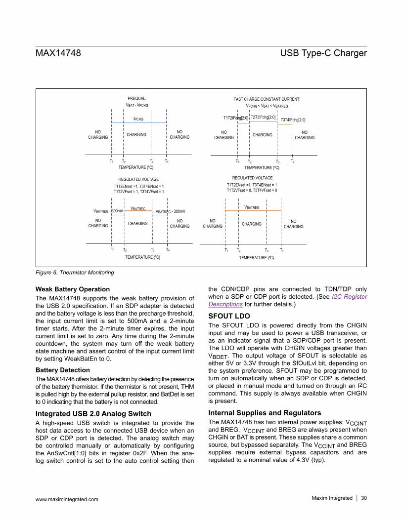
Thermistor MonitoringThe MAX14748 provides highly programmable thermal/JEITA charge management. All thermal/JEITA charge configuration parameters are set via the ThermCfg reg-isters 0x1A - 0x1C. The charger is managed by thermal information only if JEITACtrSet = 1.The battery pack temperature is measured from a divider formed by a pull-up resistor, an optional parallel resistor, and the battery pack thermistor. When required, the pullup resistor is connected to an internal supply through the TPU input, and the voltage on the THM pin is compared to an internal threshold. The supply voltage for the divider is applied to the VTPU pin and may be connected to an external supply or to VCCINT. The pullup resistor may be complemented with an additional parallel resistor to allow matching to different thermistor nominal values and charging cutoff temperatures, T1, T2, T3, and T4. There are two sets of cutoff temperatures optimized for a thermistor with Beta = 3380 (0°C/10°C/45°C/60°C or 0°C/10°C/25°C/45°C) which can be selected as factory default options. These cutoff temperatures divide the temperature range into three zones, T1_T2, T2_T3, and T3_T4. The charger is always turned off at temperatures outside these zones when any thermal monitoring mode is enabled. If the system needs to measure the THM temperature when not charging, the internal pullup switch may be enabled via the JeitaCfgR[1:0] bits.Charging may be optionally disabled in the T1_T2 and T3_T4 zones through the T_T_EnSet bits. The charge current in each zone may be modified through T_T_IFchg[2:0]. Battery-voltage termination reduction may also be selectively applied through the T_T_VFset bits. See Figure 6 for more details.
MAX14748 USB Type-C Charger
www.maximintegrated.com Maxim Integrated │ 29
Weak Battery OperationThe MAX14748 supports the weak battery provision of the USB 2.0 specification. If an SDP adapter is detected and the battery voltage is less than the precharge threshold, the input current limit is set to 500mA and a 2-minute timer starts. After the 2-minute timer expires, the input current limit is set to zero. Any time during the 2-minute countdown, the system may turn off the weak battery state machine and assert control of the input current limit by setting WeakBatEn to 0.
Battery DetectionThe MAX14748 offers battery detection by detecting the presence of the battery thermistor. If the thermistor is not present, THM is pulled high by the external pullup resistor, and BatDet is set to 0 indicating that the battery is not connected.
Integrated USB 2.0 Analog SwitchA high-speed USB switch is integrated to provide the host data access to the connected USB device when an SDP or CDP port is detected. The analog switch may be controlled manually or automatically by configuring the AnSwCntl[1:0] bits in register 0x2F. When the ana-log switch control is set to the auto control setting then
the CDN/CDP pins are connected to TDN/TDP only when a SDP or CDP port is detected. (See I2C Register Descriptions for further details.)
SFOUT LDOThe SFOUT LDO is powered directly from the CHGIN input and may be used to power a USB transceiver, or as an indicator signal that a SDP/CDP port is present. The LDO will operate with CHGIN voltages greater than VBDET. The output voltage of SFOUT is selectable as either 5V or 3.3V through the SfOutLvl bit, depending on the system preference. SFOUT may be programmed to turn on automatically when an SDP or CDP is detected, or placed in manual mode and turned on through an I2C command. This supply is always available when CHGIN is present.
Internal Supplies and RegulatorsThe MAX14748 has two internal power supplies: VCCINT and BREG. VCCINT and BREG are always present when CHGIN or BAT is present. These supplies share a common source, but bypassed separately. The VCCINT and BREG supplies require external bypass capacitors and are regulated to a nominal value of 4.3V (typ).
Figure 6. Thermistor Monitoring
T1 T4
TEMPERATURE (ºC)
CHARGINGNO
CHARGINGNO
CHARGING
T2 T3
IPCHG
PREQUAL:
VBAT < VPCHG
T1 T4
TEMPERATURE (ºC)
CHARGINGNO
CHARGINGNO
CHARGING
T2 T3
T1T2IFchg[2:0]
FAST CHARGE CONSTANT CURRENT:
VPCHG < VBAT < VBATREG
T2T3IFchg[2:0]
T1 T4
TEMPERATURE (ºC)
CHARGINGNO
CHARGING
T2 T3
VBATREG
REGULATED VOLTAGE
NO CHARGING
T1 T4
TEMPERATURE (ºC)
CHARGINGNO
CHARGING
T2 T3
VBATREG
REGULATED VOLTAGE
NO CHARGING
VBATREG - 300mV
T3T4IFchg[2:0]
T1T2ENset =1, T3T4ENset = 1T1T2VFset = 1, T3T4VFset = 1
T1T2ENset =1, T3T4ENset = 1T1T2VFset = 0, T3T4VFset = 0
VBATREG - 300mV
MAX14748 USB Type-C Charger
www.maximintegrated.com Maxim Integrated │ 30
Device Control InterfaceWhile the MAX14748 is primarily controlled by I2C, GPIO control is also offered for specific functions. The following GPIO control signals are provided (note that these signals only apply when CHGIN is present): 1) FSUS (Input): Force Suspend. This pin enables the
host microcontroller to force the input current limit to zero. When CHGIN is present, a logic-high on the pin causes the input OVP FET at CHGIN to open and the input current to MAX14748 is reduced to less than 2mA. This pin has no effect if FSUSMsk = 1.
2) FLTIN (Input): Battery Fault Input. This pin allows the system or battery pack to place the charger into a fault condition using a GPIO pin. See Register 0x35 description for more details.
3) CDIR (Open-Drain Output): USB Superspeed MUX control. In USB Type-C plug configurations, it is necessary to detect the orientation of the connector and route the Superspeed lines accordingly. The pin can be used to automatically configure a USB Super-speed MUX according to the orientation information contained in the integrated Type-C detection block. (This information is also available through I2C) The
CDIR output is pulled to GND when the CC1 pin is active on the Type-C connector, otherwise it is high-impedance.
4) SYSOK (Open-Drain Output): With CHGIN present, the SYSOK output is asserted if the boost regulator generates a VSYS greater than SYS UVLO threshold, VSYSUVLO. Otherwise, the output is high-impedance. This pin can be used as wake up the host system from a dead-battery. Note that when VSYS falls below the SYS UVLO falling threshold, the input OVP switch is opened as the boost converter cannot operate in this state.
5) BVCEN (Open-Drain Output): When CHGIN is present and a Type-C device that requires VCONN is found, this pin is asserted. This pin should be con-nected to the enable pin of the VCONN power supply enable. The output of BVCEN is push-pull between GND and VCCINT.
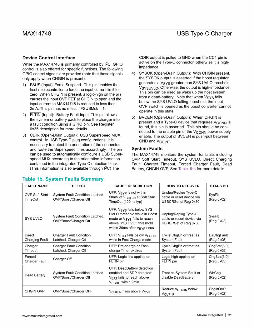
System FaultsThe MAX14748 monitors the system for faults including OVP Soft Start Timeout, SYS UVLO, Direct Charging Fault, Charger TImeout, Forced Charger Fault, Dead Battery, CHGIN OVP. See Table 1bb for more details.
Table 1b. System Faults SummaryFAULT NAME EFFECT CAUSE DESCRIPTION HOW TO RECOVER STAUS BIT
OVP Soft-Start TimeOut
System Fault Condition Latched. OVP/Boost/Charger Off
UFP: VBYP is not within 50mV of VCHGIN at Soft Start TimeOut (100ms typ)
Unplug/Replug Type-C cable or reset device via USBCRSet of Reg 0x30
SysFlt (Reg 0x02)
SYS UVLO System Fault Condition Latched. OVP/Boost/Charger Off
UFP: VSYS falls below SYS UVLO threshold while in Boost mode or VSYS fails to reach above SYS UVLO threshold within 20ms after VBYP rises
Unplug/Replug Type-C cable or resert device via USBCRSet of Reg 0x30
SysFlt (Reg 0x02)
Direct Charging Fault
Charger Fault Condition Latched. Charger Off
UFP: VBAT falls below VPCHG while in Fast Charge mode
Cycle ChgEn or treat as System Fault
DirChgFault (Reg 0x05)
Charger Timeout
Charger Fault Condition Latched. Charger Off
UFP: Pre-charge or Fast-charge Timer expires
Cycle ChgEn or treat as System Fault
ChgStat[3:0] (Reg 0x05)
Forced Charger Fault Charger Off UFP: Logic-low applied on
FLTIN pin Logic-high applied on FLTIN pin
ChgStat[3:0](Reg 0x05)
Dead Battery System Fault Condition Latched. OVP/Boost/Charger Off
UFP: DeadBattery detection enabled and SDP detected: VBAT fails to reach above VPCHG within 2min
Treat as System Fault or disable DeadBattery
WbChg(Reg 0x02)
CHGIN OVP OVP/Boost/Charger OFF VCHGIN rises above VOVPReduce VCHGIN below VOVP_F
ChginOVP(Reg 0x02)
MAX14748 USB Type-C Charger
www.maximintegrated.com Maxim Integrated │ 31
I2C InterfaceThe MAX14748 contain an I2C-compatible interface for data communication with a host controller (SCL and SDA). The interface supports a clock frequency of up to 400kHz. SCL and SDA require pullup resistors that are connected to a positive supply.
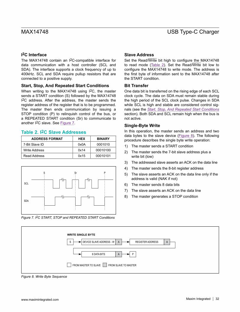
Start, Stop, And Repeated Start ConditionsWhen writing to the MAX14748 using I2C, the master sends a START condition (S) followed by the MAX14748 I2C address. After the address, the master sends the register address of the register that is to be programmed. The master then ends communication by issuing a STOP condition (P) to relinquish control of the bus, or a REPEATED START condition (Sr) to communicate to another I2C slave. See Figure 7.
Slave AddressSet the Read/Write bit high to configure the MAX14748 to read mode (Table 2). Set the Read/Write bit low to configure the MAX14748 to write mode. The address is the first byte of information sent to the MAX14748 after the START condition.
Bit TransferOne data bit is transferred on the rising edge of each SCL clock cycle. The data on SDA must remain stable during the high period of the SCL clock pulse. Changes in SDA while SCL is high and stable are considered control sig-nals (see the Start, Stop, And Repeated Start Conditions section). Both SDA and SCL remain high when the bus is not active.
Single-Byte WriteIn this operation, the master sends an address and two data bytes to the slave device (Figure 8). The following procedure describes the single byte write operation:1) The master sends a START condition2) The master sends the 7-bit slave address plus a
write bit (low)3) The addressed slave asserts an ACK on the data line4) The master sends the 8-bit register address5) The slave asserts an ACK on the data line only if the
address is valid (NAK if not)6) The master sends 8 data bits7) The slave asserts an ACK on the data line8) The master generates a STOP condition
Figure 8. Write Byte Sequence
Figure 7. I2C START, STOP and REPEATED START Conditions
Table 2. I2C Slave AddressesADDRESS FORMAT HEX BINARY
7-Bit Slave ID 0x0A 0001010Write Address 0x14 00010100Read Address 0x15 00010101
SCL
SDA
S Sr P
S
P
DEVICE SLAVE ADDRESS - W A
8 DATA BITS
WRITE SINGLE BYTE
FROM MASTER TO SLAVE FROM SLAVE TO MASTER
A
REGISTER ADDRESS A
MAX14748 USB Type-C Charger
www.maximintegrated.com Maxim Integrated │ 32
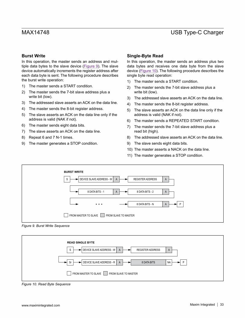
Burst WriteIn this operation, the master sends an address and mul-tiple data bytes to the slave device (Figure 9). The slave device automatically increments the register address after each data byte is sent. The following procedure describes the burst write operation:1) The master sends a START condition.2) The master sends the 7-bit slave address plus a
write bit (low).3) The addressed slave asserts an ACK on the data line.4) The master sends the 8-bit register address.5) The slave asserts an ACK on the data line only if the
address is valid (NAK if not).6) The master sends eight data bits.7) The slave asserts an ACK on the data line.8) Repeat 6 and 7 N-1 times.9) The master generates a STOP condition.
Single-Byte ReadIn this operation, the master sends an address plus two data bytes and receives one data byte from the slave device (Figure 10). The following procedure describes the single byte read operation:1) The master sends a START condition.2) The master sends the 7-bit slave address plus a
write bit (low).3) The addressed slave asserts an ACK on the data line.4) The master sends the 8-bit register address.5) The slave asserts an ACK on the data line only if the
address is valid (NAK if not).6) The master sends a REPEATED START condition.7) The master sends the 7-bit slave address plus a
read bit (high).8) The addressed slave asserts an ACK on the data line.9) The slave sends eight data bits.10) The master asserts a NACK on the data line.11) The master generates a STOP condition.
Figure 10. Read Byte Sequence
Figure 9. Burst Write Sequence
S DEVICE SLAVE ADDRESS - W A
8 DATA BITS - 1
BURST WRITE
A
REGISTER ADDRESS A
8 DATA BITS - N A
8 DATA BITS - 2 A
FROM MASTER TO SLAVE FROM SLAVE TO MASTER
P
S
Sr
DEVICE SLAVE ADDRESS - W A
DEVICE SLAVE ADDRESS - R
READ SINGLE BYTE
A
REGISTER ADDRESS A
8 DATA BITS NA
FROM MASTER TO SLAVE FROM SLAVE TO MASTER
P
MAX14748 USB Type-C Charger
www.maximintegrated.com Maxim Integrated │ 33
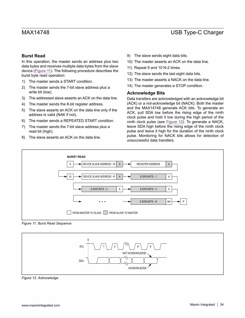
Burst ReadIn this operation, the master sends an address plus two data bytes and receives multiple data bytes from the slave device (Figure 11). The following procedure describes the burst byte read operation:1) The master sends a START condition.2) The master sends the 7-bit slave address plus a
write bit (low).3) The addressed slave asserts an ACK on the data line.4) The master sends the 8-bit register address.5) The slave asserts an ACK on the data line only if the
address is valid (NAK if not).6) The master sends a REPEATED START condition.7) The master sends the 7-bit slave address plus a
read bit (high).8) The slave asserts an ACK on the data line.
9) The slave sends eight data bits.10) The master asserts an ACK on the data line.11) Repeat 9 and 10 N-2 times.12) The slave sends the last eight data bits.13) The master asserts a NACK on the data line.14) The master generates a STOP condition.
Acknowledge BitsData transfers are acknowledged with an acknowledge bit (ACK) or a not-acknowledge bit (NACK). Both the master and the MAX14748 generate ACK bits. To generate an ACK, pull SDA low before the rising edge of the ninth clock pulse and hold it low during the high period of the ninth clock pulse (see Figure 12). To generate a NACK, leave SDA high before the rising edge of the ninth clock pulse and leave it high for the duration of the ninth clock pulse. Monitoring for NACK bits allows for detection of unsuccessful data transfers.
Figure 12. Acknowledge
Figure 11. Burst Read Sequence
S
Sr
DEVICE SLAVE ADDRESS - W A
DEVICE SLAVE ADDRESS - R
BURST READ
A
REGISTER ADDRESS A
8 DATA BITS - 1 A
A 8 DATA BITS - 38 DATA BITS - 2 A
8 DATA BITS - N NA
FROM MASTER TO SLAVE FROM SLAVE TO MASTER
P
NOT ACKNOWLEDGE
ACKNOWLEDGE
1 2 8 9
SDA
SCL
S
MAX14748 USB Type-C Charger
www.maximintegrated.com Maxim Integrated │ 34
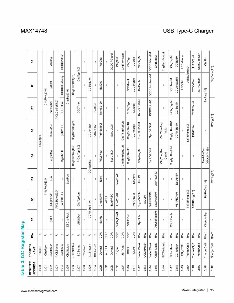
Tabl
e 3.
I2C
Reg
iste
r Map
REG
ISTE
R
AD
DR
ESS
REG
ISTE
R
NA
ME
R/W
B7
B6
B5
B4
B3
B2
B1
B0
0x00
Chi
pID
RC
hipI
d[7:
0]
0x01
Chi
pRev
RC
hipR
evH
[3:0
]C
hipR
evL[
3:0]
0x02
Dev
Stat
us1
RSy
sFlt
Chg
InO
VPIL
imVS
ysR
egTh
rmSd
150
Thrm
Sd12
0Ba
tDet
WbC
hg
0x03
AIC
LSta
tus
RAI
CLS
tatu
s[2:
0]AI
CLC
urSe
t[4:0
]
0x04
Dev
Stat
us2
R–
BattP
REQ
B–
BypU
VLO
SysU
VLO
BD
CD
CIL
imD
CD
CR
unAw
ayD
CD
CPG
ood
0x05
Chg
Stat
usR
DirC
hgFa
ult
–Lo
wPo
w–
Chg
Stat
[3:0
]
0x06
JEIT
ASta
tus
R–
––
Chg
Thrm
Reg
Cur
Chg
Thrm
Reg
Vlt
Chg
Thrm
Stat
[2:0
]
0x07
BCSt
atus
RVB
USD
etC
hgTy
pRun
PrC
hgTy
p[2:
0]D
CD
Tmo
Chg
Typ[
1:0]
0x08
Res
erve
dR
––
––
––
––
0x09
CC
Stat
us1
RC
CPi
nSta
t[1:0
]C
CIS
tat[1
:0]
CC
VcnS
tat
CC
Stat
[2:0
]
0x0A
CC
Stat
us2
R–
––
–VS
AFE0
VD
etAb
rt–
–
0x0B
Dev
Int1
CO
RSy
sFltI
Chg
InO
VPI
ILim
IVS
ysR
egI
Thrm
Sd15
0ITh
rmSd
120I
BatD
etI
WbC
hgI
0x0C
AIC
LInt
CO
R–
AIC
LI–
––
––
–
0x0D
Dev
Int2
CO
R–
BattP
REQ
i–
BypU
VLO
ISy
sUVL
OI
––
DC
DC
PGoo
dI
0x0E
Chg
Int
CO
RD
irChg
Faul
tILo
wPo
wR
ILo
wPo
wFI
––
––
Chg
Stat
I
0x0F
JEIT
AInt
CO
R–
––
Chg
Thrm
Reg
Cur
IC
hgTh
rmR
egVl
tI–
–C
hgTh
rmSt
atI
0x10
BCIn
tC
OR
VBU
SDet
I–
–C
hgTy
pRun
FIC
hgTy
pRun
RI
PrC
hgTy
pID
CD
TmoI
Chg
TypI
0x11
CC
Int
CO
R–
VSAF
E0VI
Det
AbrtI
CC
PinS
tatI
CC
ISta
tIC
CVc
nSta
tIC
CSt
atI
0x12
Dev
Int1
Mas
kR
/WSy
sFltI
MC
hgIn
OVP
IMIL
imIM
VSys
Reg
IMTh
rmSd
150I
MTh
rmSd
120I
MBa
tDet
IMW
bChg
IM
0x13
AIC
LInt
Mas
kR
/W–
AIC
LIM
––
––
––
0x14
Dev
Int2
Mas
kR
/W–
BattP
REQ
IM–
BypU
VLO
IMSy
sUVL
OIM
DC
DC
ILim
IMD
CD
CR
unAw
ayIM
DC
DC
PGoo
dIM
0x15
Chg
IntM
ask
R/W
DirC
hgFa
ultIM
Low
Pow
RIM
Low
Pow
FIM
––
––
Chg
Stat
IM
0x16
JEIT
AInt
Mas
kR
/W–
––
Chg
Thrm
Reg
Cur
IMC
hgTh
rmR
egVl
tIM–
–C
hgTh
rmSt
atIM
0x17
BCIn
tMas
kR
/WVB
USD
etIM
––
Chg
TypR
unFI
MC
hgTy
pRun
RIM
PrC
hgTy
pIM
DC
DTm
oIM
Chg
TypI
M
0x18
CC
IntM
ask
R/W
–VS
AFE0
VIM
Det
AbrtI
M–
CC
PinS
tatIM
CC
ISta
tIMC
CVc
nSta
tIMC
CSt
atIM
0x19
LED
_CTR
LR
/W–
––
––
–LE
DC
trlLE
DM
anua
l
0x1A
Ther
maC
fg1
R/W
T1T2
IFch
g[2:
0]T2
T3IF
chg[
2:0]
Jeita
Cfg
R[1
:0]
0x1B
Ther
maC
fg2
R/W
T3T4
IFch
g[2:
0]–
T3T4
ENse
tT1
T2EN
set
T3T4
VFse
tT1
T2VF
set
0x1C
Ther
maC
fg3
R/W
––
––
––
JEIT
ACtrS
etW
arm
Coo
lSel
*
0x1D
Cha
rger
Ctrl
1R
/W**
Chg
Auto
Stp
BatR
eChg
[1:0
]Fr
eshB
atD
is
(MAX
1474
8B)
–Ba
tReg
[1:0
]C
hgEn
0x1E
Cha
rger
Ctrl
2R
/W**
–VP
chg[
2:0]
IPC
hg[1
:0]
Chg
Don
e[1:
0]
MAX14748 USB Type-C Charger
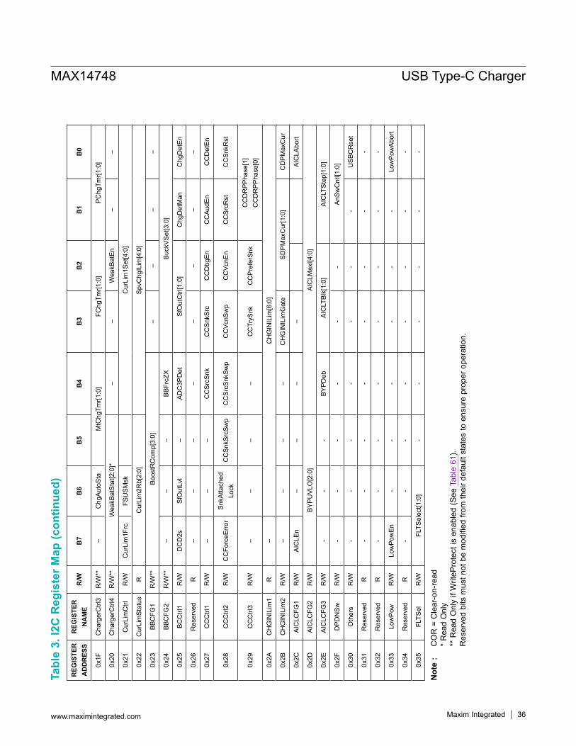
www.maximintegrated.com Maxim Integrated │ 35
Not
e :
CO
R =
Cle
ar-o
n-re
ad
* R
ead
Onl
y
** R
ead
Onl
y if
Writ
ePro
tect
is e
nabl
ed (S
ee T
able
61)
.
Res
erve
d bi
ts m
ust n
ot b
e m
odifi
ed fr
om th
eir d
efau
lt st
ates
to e
nsur
e pr
oper
ope
ratio
n.
Tabl
e 3.
I2C
Reg
iste
r Map
(con
tinue
d)R
EGIS
TER
A
DD
RES
SR
EGIS
TER
N
AM
ER
/WB
7B
6B
5B
4B
3B
2B
1B
0
0x1F
Cha
rger
Ctrl
3R
/W**
–C
hgAu
toSt
aM
tChg
Tmr[1
:0]
FChg
Tmr[1
:0]
PChg
Tmr[1
:0]
0x20
Cha
rger
Ctrl
4R
/W**
Wea
kBat
Stat
[2:0
]*–
–W
eakB
atEn
––
0x21
Cur
Lim
Ctrl
R/W
Cur
Lim
1Frc
FSU
SMsk
Cur
Lim
1Set
[4:0
]
0x22
Cur
Lim
Stat
usR
Cur
Lim
2Rb[
2:0]
SpvC
hgIL
im[4
:0]
0x23
BBC
FG1
R/W
**Bo
ostR
Com
p[3:
0]–
––
–
0x24
BBC
FG2
R/W
**–
––
BBFr
cZX
Buck
VSet
[3:0
]
0x25
BCC
trl1
R/W
DC
D2s
SfO
utLv
l–
ADC
3PD
etSf
Out
Ctrl
[1:0
]C
hgD
etM
anC
hgD
etEn
0x26
Res
erve
dR
––
––
––
––
0x27
CC
Ctrl
1R
/W–
––
CC
SrcS
nkC
CSn
kSrc
CC
Dbg
EnC
CAu
dEn
CC
Det
En
0x28
CC
Ctrl
2R
/WC
CFo
rceE
rror
SnkA
ttach
edLo
ckC
CSn
kSrc
Swp
CC
SrcS
nkSw
pC
CVc
nSw
pC
CVc
nEn
CC
SrcR
stC
CSn
kRst
0x29
CC
Ctrl
3R
/W–
––
–C
CTr
ySnk
CC
Pref
erSn
kC
CD
RPP
hase
[1]
CC
DR
PPha
se[0
]
0x2A
CH
GIN
ILim
1R
–C
HG
INIL
im[6
:0]
0x2B
CH
GIN
ILim
2R
/W–
––
–C
HG
INIL
imG
ate
SDPM
axC
ur[1
:0]
CD
PMax
Cur
0x2C
AIC
LCFG
1R
/WAI
CLE
n–
––
–AI
CLA
bort
0x2D
AIC
LCFG
2R
/WBY
PUVL
O[2
:0]
AIC
LMax
I[4:0
]
0x2E
AIC
LCFG
3R
/W-
--
BYPD
ebAI
CLT
Blk[
1:0]
AIC
LTSt
ep[1
:0]
0x2F
DPD
NSw
R/W
--
--
--
AnSw
Cnt
l[1:0
]
0x30
Oth
ers
R/W
--
--
--
-U
SBC
Rse
t
0x31
Res
erve
dR
--
--
--
--
0x32
Res
erve
dR
--
--
--
--
0x33
Low
Pow
R/W
Low
Pow
En-
--
--
-Lo
wPo
wAb
ort
0x34
Res
erve
dR
--
--
--
--
0x35
FLTS
elR
/WFL
TSel
ect[1
:0]
--
--
--
MAX14748 USB Type-C Charger
www.maximintegrated.com Maxim Integrated │ 36
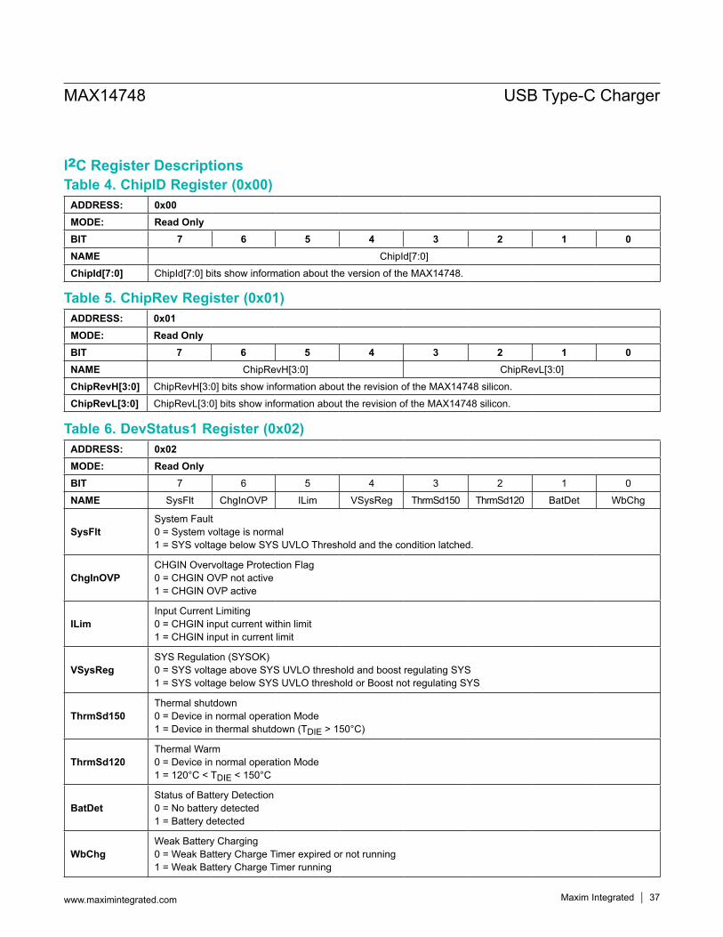
Table 6. DevStatus1 Register (0x02)
Table 5. ChipRev Register (0x01)
Table 4. ChipID Register (0x00)ADDRESS: 0x00MODE: Read OnlyBIT 7 6 5 4 3 2 1 0NAME ChipId[7:0]ChipId[7:0] ChipId[7:0] bits show information about the version of the MAX14748.
ADDRESS: 0x01MODE: Read OnlyBIT 7 6 5 4 3 2 1 0NAME ChipRevH[3:0] ChipRevL[3:0]ChipRevH[3:0] ChipRevH[3:0] bits show information about the revision of the MAX14748 silicon.ChipRevL[3:0] ChipRevL[3:0] bits show information about the revision of the MAX14748 silicon.
ADDRESS: 0x02MODE: Read OnlyBIT 7 6 5 4 3 2 1 0NAME SysFlt ChgInOVP ILim VSysReg ThrmSd150 ThrmSd120 BatDet WbChg
SysFltSystem Fault0 = System voltage is normal1 = SYS voltage below SYS UVLO Threshold and the condition latched.
ChgInOVPCHGIN Overvoltage Protection Flag 0 = CHGIN OVP not active 1 = CHGIN OVP active
ILimInput Current Limiting 0 = CHGIN input current within limit 1 = CHGIN input in current limit
VSysRegSYS Regulation (SYSOK)0 = SYS voltage above SYS UVLO threshold and boost regulating SYS 1 = SYS voltage below SYS UVLO threshold or Boost not regulating SYS
ThrmSd150Thermal shutdown 0 = Device in normal operation Mode 1 = Device in thermal shutdown (TDIE > 150°C)
ThrmSd120Thermal Warm 0 = Device in normal operation Mode 1 = 120°C < TDIE < 150°C
BatDetStatus of Battery Detection 0 = No battery detected 1 = Battery detected
WbChgWeak Battery Charging 0 = Weak Battery Charge Timer expired or not running1 = Weak Battery Charge Timer running
MAX14748 USB Type-C Charger
www.maximintegrated.com Maxim Integrated │ 37
I2C Register Descriptions
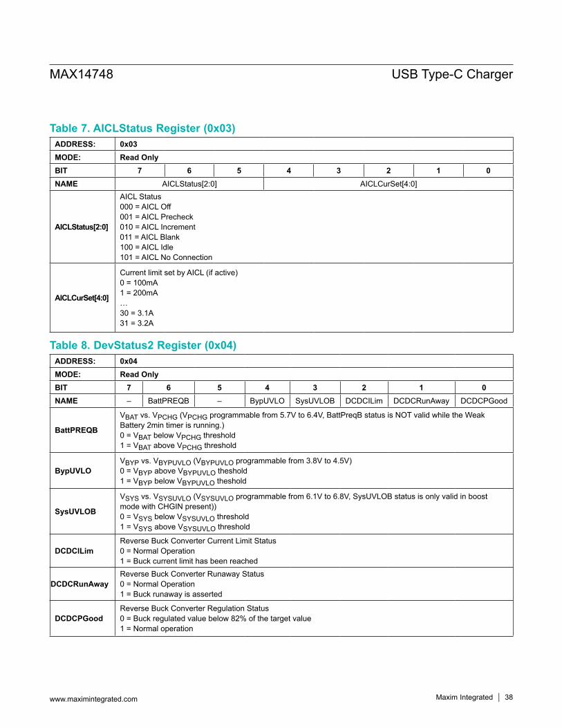
Table 8. DevStatus2 Register (0x04)
Table 7. AICLStatus Register (0x03)ADDRESS: 0x03MODE: Read OnlyBIT 7 6 5 4 3 2 1 0NAME AICLStatus[2:0] AICLCurSet[4:0]
AICLStatus[2:0]
AICL Status 000 = AICL Off001 = AICL Precheck010 = AICL Increment011 = AICL Blank100 = AICL Idle101 = AICL No Connection
AICLCurSet[4:0]
Current limit set by AICL (if active) 0 = 100mA 1 = 200mA…30 = 3.1A31 = 3.2A
ADDRESS: 0x04MODE: Read OnlyBIT 7 6 5 4 3 2 1 0NAME – BattPREQB – BypUVLO SysUVLOB DCDCILim DCDCRunAway DCDCPGood
BattPREQB
VBAT vs. VPCHG (VPCHG programmable from 5.7V to 6.4V, BattPreqB status is NOT valid while the Weak Battery 2min timer is running.) 0 = VBAT below VPCHG threshold 1 = VBAT above VPCHG threshold
BypUVLOVBYP vs. VBYPUVLO (VBYPUVLO programmable from 3.8V to 4.5V) 0 = VBYP above VBYPUVLO theshold 1 = VBYP below VBYPUVLO theshold
SysUVLOB
VSYS vs. VSYSUVLO (VSYSUVLO programmable from 6.1V to 6.8V, SysUVLOB status is only valid in boost mode with CHGIN present)) 0 = VSYS below VSYSUVLO threshold 1 = VSYS above VSYSUVLO threshold
DCDCILimReverse Buck Converter Current Limit Status 0 = Normal Operation 1 = Buck current limit has been reached
DCDCRunAwayReverse Buck Converter Runaway Status 0 = Normal Operation 1 = Buck runaway is asserted
DCDCPGoodReverse Buck Converter Regulation Status 0 = Buck regulated value below 82% of the target value 1 = Normal operation
MAX14748 USB Type-C Charger
www.maximintegrated.com Maxim Integrated │ 38
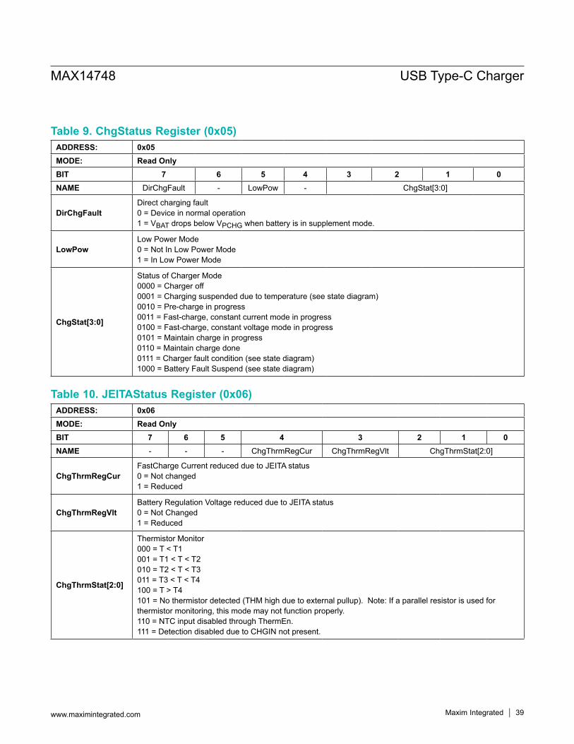
Table 10. JEITAStatus Register (0x06)
Table 9. ChgStatus Register (0x05)ADDRESS: 0x05MODE: Read OnlyBIT 7 6 5 4 3 2 1 0NAME DirChgFault - LowPow - ChgStat[3:0]
DirChgFaultDirect charging fault 0 = Device in normal operation 1 = VBAT drops below VPCHG when battery is in supplement mode.
LowPowLow Power Mode0 = Not In Low Power Mode1 = In Low Power Mode
ChgStat[3:0]
Status of Charger Mode 0000 = Charger off 0001 = Charging suspended due to temperature (see state diagram) 0010 = Pre-charge in progress 0011 = Fast-charge, constant current mode in progress0100 = Fast-charge, constant voltage mode in progress0101 = Maintain charge in progress 0110 = Maintain charge done 0111 = Charger fault condition (see state diagram)1000 = Battery Fault Suspend (see state diagram)
ADDRESS: 0x06MODE: Read OnlyBIT 7 6 5 4 3 2 1 0NAME - - - ChgThrmRegCur ChgThrmRegVlt ChgThrmStat[2:0]
ChgThrmRegCurFastCharge Current reduced due to JEITA status0 = Not changed1 = Reduced
ChgThrmRegVltBattery Regulation Voltage reduced due to JEITA status0 = Not Changed1 = Reduced
ChgThrmStat[2:0]
Thermistor Monitor 000 = T < T1 001 = T1 < T < T2 010 = T2 < T < T3 011 = T3 < T < T4 100 = T > T4 101 = No thermistor detected (THM high due to external pullup). Note: If a parallel resistor is used for thermistor monitoring, this mode may not function properly. 110 = NTC input disabled through ThermEn. 111 = Detection disabled due to CHGIN not present.
MAX14748 USB Type-C Charger
www.maximintegrated.com Maxim Integrated │ 39
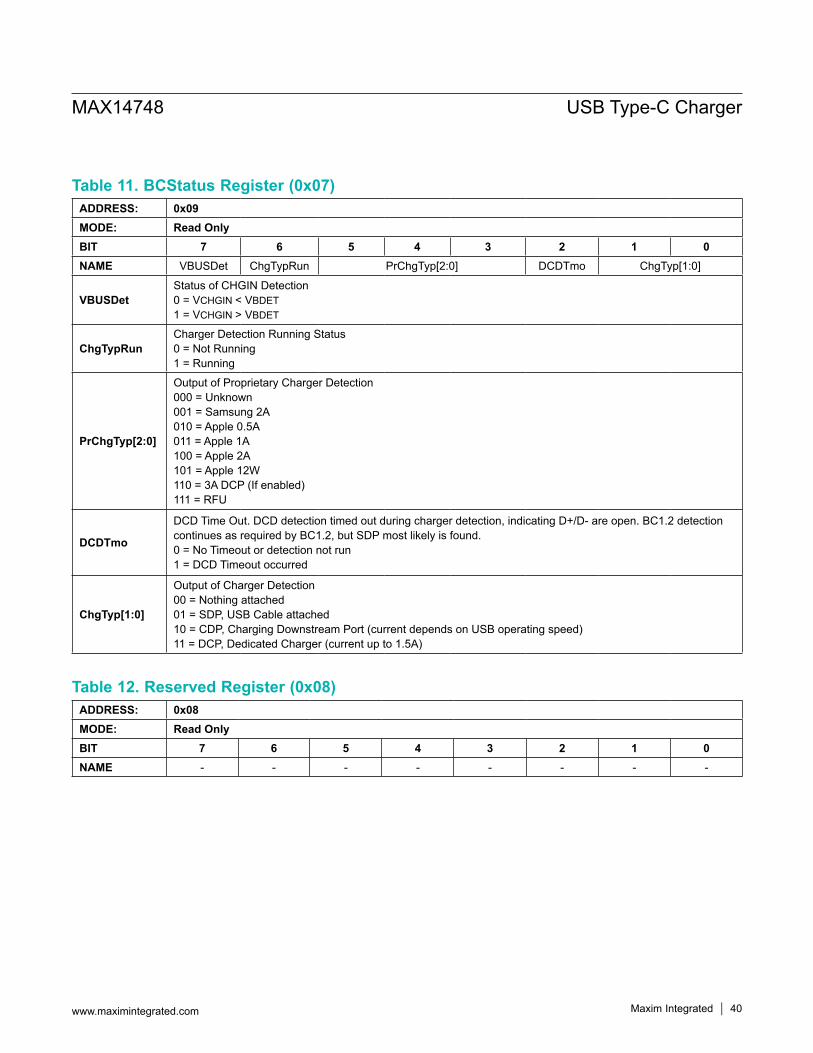
Table 12. Reserved Register (0x08)
Table 11. BCStatus Register (0x07)ADDRESS: 0x09MODE: Read OnlyBIT 7 6 5 4 3 2 1 0NAME VBUSDet ChgTypRun PrChgTyp[2:0] DCDTmo ChgTyp[1:0]
VBUSDetStatus of CHGIN Detection 0 = VCHGIN < VBDET 1 = VCHGIN > VBDET
ChgTypRunCharger Detection Running Status 0 = Not Running 1 = Running
PrChgTyp[2:0]
Output of Proprietary Charger Detection 000 = Unknown 001 = Samsung 2A 010 = Apple 0.5A 011 = Apple 1A 100 = Apple 2A 101 = Apple 12W 110 = 3A DCP (If enabled) 111 = RFU
DCDTmo
DCD Time Out. DCD detection timed out during charger detection, indicating D+/D- are open. BC1.2 detection continues as required by BC1.2, but SDP most likely is found. 0 = No Timeout or detection not run 1 = DCD Timeout occurred
ChgTyp[1:0]
Output of Charger Detection 00 = Nothing attached 01 = SDP, USB Cable attached 10 = CDP, Charging Downstream Port (current depends on USB operating speed) 11 = DCP, Dedicated Charger (current up to 1.5A)
ADDRESS: 0x08MODE: Read OnlyBIT 7 6 5 4 3 2 1 0NAME - - - - - - - -
MAX14748 USB Type-C Charger
www.maximintegrated.com Maxim Integrated │ 40
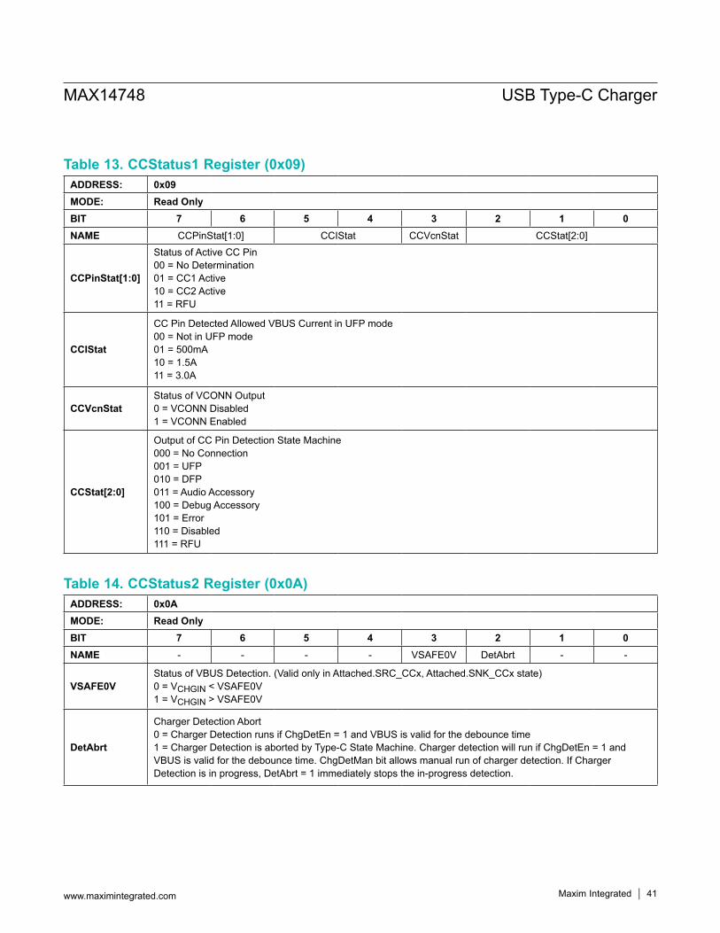
Table 14. CCStatus2 Register (0x0A)
Table 13. CCStatus1 Register (0x09)ADDRESS: 0x09MODE: Read OnlyBIT 7 6 5 4 3 2 1 0NAME CCPinStat[1:0] CCIStat CCVcnStat CCStat[2:0]
CCPinStat[1:0]
Status of Active CC Pin 00 = No Determination 01 = CC1 Active 10 = CC2 Active 11 = RFU
CCIStat
CC Pin Detected Allowed VBUS Current in UFP mode 00 = Not in UFP mode 01 = 500mA 10 = 1.5A 11 = 3.0A
CCVcnStatStatus of VCONN Output 0 = VCONN Disabled 1 = VCONN Enabled
CCStat[2:0]
Output of CC Pin Detection State Machine 000 = No Connection 001 = UFP 010 = DFP 011 = Audio Accessory 100 = Debug Accessory 101 = Error 110 = Disabled 111 = RFU
ADDRESS: 0x0AMODE: Read OnlyBIT 7 6 5 4 3 2 1 0NAME - - - - VSAFE0V DetAbrt - -
VSAFE0VStatus of VBUS Detection. (Valid only in Attached.SRC_CCx, Attached.SNK_CCx state)0 = VCHGIN < VSAFE0V 1 = VCHGIN > VSAFE0V
DetAbrt
Charger Detection Abort0 = Charger Detection runs if ChgDetEn = 1 and VBUS is valid for the debounce time 1 = Charger Detection is aborted by Type-C State Machine. Charger detection will run if ChgDetEn = 1 and VBUS is valid for the debounce time. ChgDetMan bit allows manual run of charger detection. If Charger Detection is in progress, DetAbrt = 1 immediately stops the in-progress detection.
MAX14748 USB Type-C Charger
www.maximintegrated.com Maxim Integrated │ 41
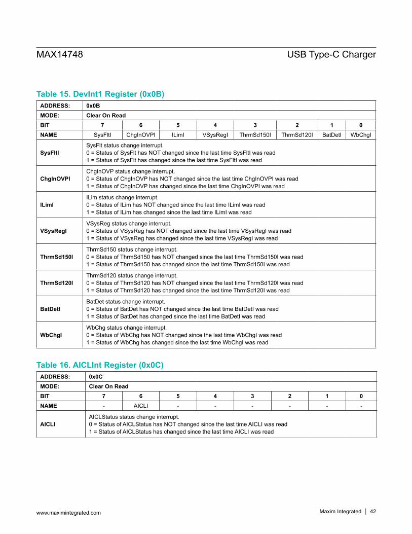
Table 16. AICLInt Register (0x0C)
Table 15. DevInt1 Register (0x0B)ADDRESS: 0x0BMODE: Clear On ReadBIT 7 6 5 4 3 2 1 0NAME SysFltI ChgInOVPI ILimI VSysRegI ThrmSd150I ThrmSd120I BatDetI WbChgI
SysFltISysFlt status change interrupt. 0 = Status of SysFlt has NOT changed since the last time SysFltI was read 1 = Status of SysFlt has changed since the last time SysFltI was read
ChgInOVPIChgInOVP status change interrupt. 0 = Status of ChgInOVP has NOT changed since the last time ChgInOVPI was read 1 = Status of ChgInOVP has changed since the last time ChgInOVPI was read
ILimIILim status change interrupt. 0 = Status of ILim has NOT changed since the last time ILimI was read 1 = Status of ILim has changed since the last time ILimI was read
VSysRegIVSysReg status change interrupt. 0 = Status of VSysReg has NOT changed since the last time VSysRegI was read 1 = Status of VSysReg has changed since the last time VSysRegI was read
ThrmSd150IThrmSd150 status change interrupt. 0 = Status of ThrmSd150 has NOT changed since the last time ThrmSd150I was read 1 = Status of ThrmSd150 has changed since the last time ThrmSd150I was read
ThrmSd120IThrmSd120 status change interrupt.0 = Status of ThrmSd120 has NOT changed since the last time ThrmSd120I was read 1 = Status of ThrmSd120 has changed since the last time ThrmSd120I was read
BatDetIBatDet status change interrupt. 0 = Status of BatDet has NOT changed since the last time BatDetI was read 1 = Status of BatDet has changed since the last time BatDetI was read
WbChgIWbChg status change interrupt. 0 = Status of WbChg has NOT changed since the last time WbChgI was read 1 = Status of WbChg has changed since the last time WbChgI was read
ADDRESS: 0x0CMODE: Clear On ReadBIT 7 6 5 4 3 2 1 0NAME - AICLI - - - - - -
AICLIAICLStatus status change interrupt. 0 = Status of AICLStatus has NOT changed since the last time AICLI was read 1 = Status of AICLStatus has changed since the last time AICLI was read
MAX14748 USB Type-C Charger
www.maximintegrated.com Maxim Integrated │ 42
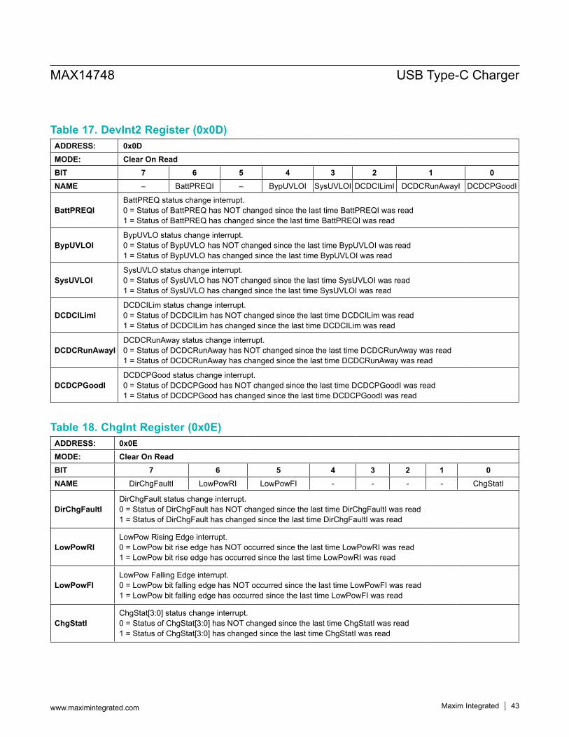
Table 18. ChgInt Register (0x0E)
Table 17. DevInt2 Register (0x0D)ADDRESS: 0x0DMODE: Clear On ReadBIT 7 6 5 4 3 2 1 0NAME – BattPREQI – BypUVLOI SysUVLOI DCDCILimI DCDCRunAwayI DCDCPGoodI
BattPREQIBattPREQ status change interrupt. 0 = Status of BattPREQ has NOT changed since the last time BattPREQI was read 1 = Status of BattPREQ has changed since the last time BattPREQI was read
BypUVLOIBypUVLO status change interrupt. 0 = Status of BypUVLO has NOT changed since the last time BypUVLOI was read 1 = Status of BypUVLO has changed since the last time BypUVLOI was read
SysUVLOISysUVLO status change interrupt. 0 = Status of SysUVLO has NOT changed since the last time SysUVLOI was read 1 = Status of SysUVLO has changed since the last time SysUVLOI was read
DCDCILimIDCDCILim status change interrupt. 0 = Status of DCDCILim has NOT changed since the last time DCDCILim was read1 = Status of DCDCILim has changed since the last time DCDCILim was read
DCDCRunAwayIDCDCRunAway status change interrupt. 0 = Status of DCDCRunAway has NOT changed since the last time DCDCRunAway was read1 = Status of DCDCRunAway has changed since the last time DCDCRunAway was read
DCDCPGoodIDCDCPGood status change interrupt. 0 = Status of DCDCPGood has NOT changed since the last time DCDCPGoodI was read 1 = Status of DCDCPGood has changed since the last time DCDCPGoodI was read
ADDRESS: 0x0EMODE: Clear On ReadBIT 7 6 5 4 3 2 1 0NAME DirChgFaultI LowPowRI LowPowFI - - - - ChgStatI
DirChgFaultIDirChgFault status change interrupt. 0 = Status of DirChgFault has NOT changed since the last time DirChgFaultI was read 1 = Status of DirChgFault has changed since the last time DirChgFaultI was read
LowPowRILowPow Rising Edge interrupt. 0 = LowPow bit rise edge has NOT occurred since the last time LowPowRI was read 1 = LowPow bit rise edge has occurred since the last time LowPowRI was read
LowPowFILowPow Falling Edge interrupt. 0 = LowPow bit falling edge has NOT occurred since the last time LowPowFI was read 1 = LowPow bit falling edge has occurred since the last time LowPowFI was read
ChgStatIChgStat[3:0] status change interrupt. 0 = Status of ChgStat[3:0] has NOT changed since the last time ChgStatI was read 1 = Status of ChgStat[3:0] has changed since the last time ChgStatI was read
MAX14748 USB Type-C Charger
www.maximintegrated.com Maxim Integrated │ 43
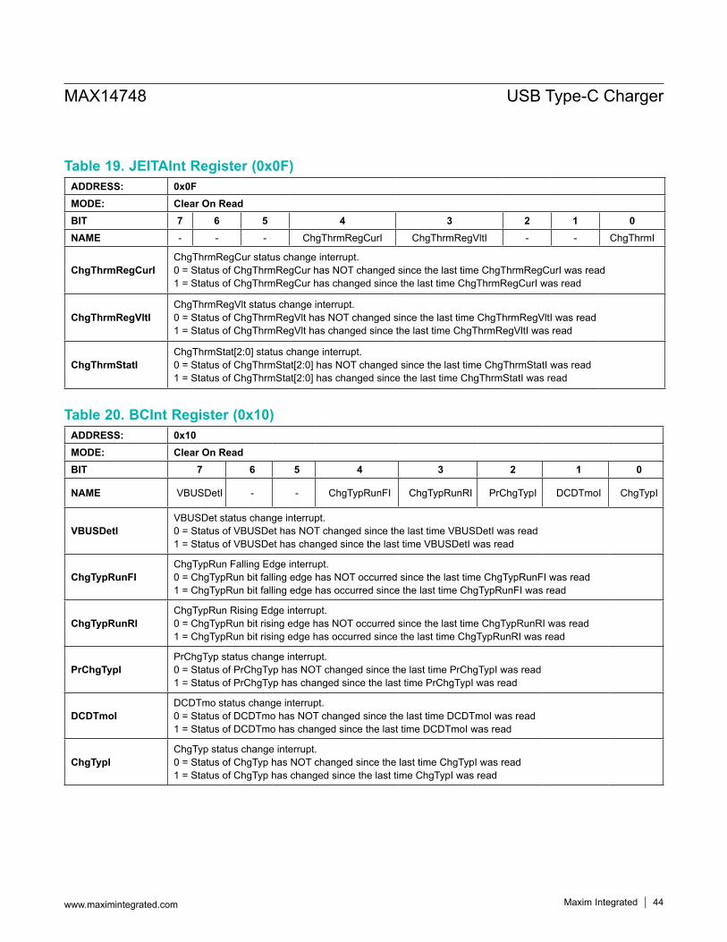
Table 20. BCInt Register (0x10)
Table 19. JEITAInt Register (0x0F)ADDRESS: 0x0FMODE: Clear On ReadBIT 7 6 5 4 3 2 1 0NAME - - - ChgThrmRegCurI ChgThrmRegVltI - - ChgThrmI
ChgThrmRegCurIChgThrmRegCur status change interrupt. 0 = Status of ChgThrmRegCur has NOT changed since the last time ChgThrmRegCurI was read 1 = Status of ChgThrmRegCur has changed since the last time ChgThrmRegCurI was read
ChgThrmRegVltIChgThrmRegVlt status change interrupt. 0 = Status of ChgThrmRegVlt has NOT changed since the last time ChgThrmRegVltI was read 1 = Status of ChgThrmRegVlt has changed since the last time ChgThrmRegVltI was read
ChgThrmStatIChgThrmStat[2:0] status change interrupt. 0 = Status of ChgThrmStat[2:0] has NOT changed since the last time ChgThrmStatI was read 1 = Status of ChgThrmStat[2:0] has changed since the last time ChgThrmStatI was read
ADDRESS: 0x10MODE: Clear On ReadBIT 7 6 5 4 3 2 1 0
NAME VBUSDetI - - ChgTypRunFI ChgTypRunRI PrChgTypI DCDTmoI ChgTypI
VBUSDetIVBUSDet status change interrupt. 0 = Status of VBUSDet has NOT changed since the last time VBUSDetI was read 1 = Status of VBUSDet has changed since the last time VBUSDetI was read
ChgTypRunFIChgTypRun Falling Edge interrupt. 0 = ChgTypRun bit falling edge has NOT occurred since the last time ChgTypRunFI was read 1 = ChgTypRun bit falling edge has occurred since the last time ChgTypRunFI was read
ChgTypRunRIChgTypRun Rising Edge interrupt. 0 = ChgTypRun bit rising edge has NOT occurred since the last time ChgTypRunRI was read 1 = ChgTypRun bit rising edge has occurred since the last time ChgTypRunRI was read
PrChgTypIPrChgTyp status change interrupt. 0 = Status of PrChgTyp has NOT changed since the last time PrChgTypI was read 1 = Status of PrChgTyp has changed since the last time PrChgTypI was read
DCDTmoIDCDTmo status change interrupt. 0 = Status of DCDTmo has NOT changed since the last time DCDTmoI was read 1 = Status of DCDTmo has changed since the last time DCDTmoI was read
ChgTypIChgTyp status change interrupt. 0 = Status of ChgTyp has NOT changed since the last time ChgTypI was read 1 = Status of ChgTyp has changed since the last time ChgTypI was read
MAX14748 USB Type-C Charger
www.maximintegrated.com Maxim Integrated │ 44
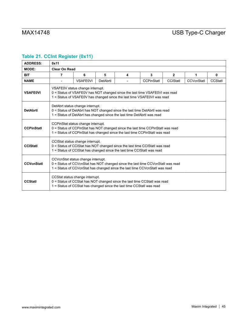
Table 21. CCInt Register (0x11)ADDRESS: 0x11MODE: Clear On ReadBIT 7 6 5 4 3 2 1 0NAME - VSAFE0VI DetAbrtI - CCPinStatI CCIStatI CCVcnStatI CCStatI
VSAFE0VIVSAFE0V status change interrupt. 0 = Status of VSAFE0V has NOT changed since the last time VSAFE0VI was read 1 = Status of VSAFE0V has changed since the last time VSAFE0VI was read
DetAbrtIDetAbrt status change interrupt. 0 = Status of DetAbrt has NOT changed since the last time DetAbrtI was read 1 = Status of DetAbrt has changed since the last time DetAbrtI was read
CCPinStatICCPinStat status change interrupt. 0 = Status of CCPinStat has NOT changed since the last time CCPinStatI was read 1 = Status of CCPinStat has changed since the last time CCPinStatI was read
CCIStatICCIStat status change interrupt. 0 = Status of CCIStat has NOT changed since the last time CCIStatI was read 1 = Status of CCIStat has changed since the last time CCIStatI was read
CCVcnStatICCVcnStat status change interrupt. 0 = Status of CCVcnStat has NOT changed since the last time CCVcnStatI was read 1 = Status of CCVcnStat has changed since the last time CCVcnStatI was read
CCStatICCStat status change interrupt. 0 = Status of CCStat has NOT changed since the last time CCStatI was read 1 = Status of CCStat has changed since the last time CCStatI was read
MAX14748 USB Type-C Charger
www.maximintegrated.com Maxim Integrated │ 45
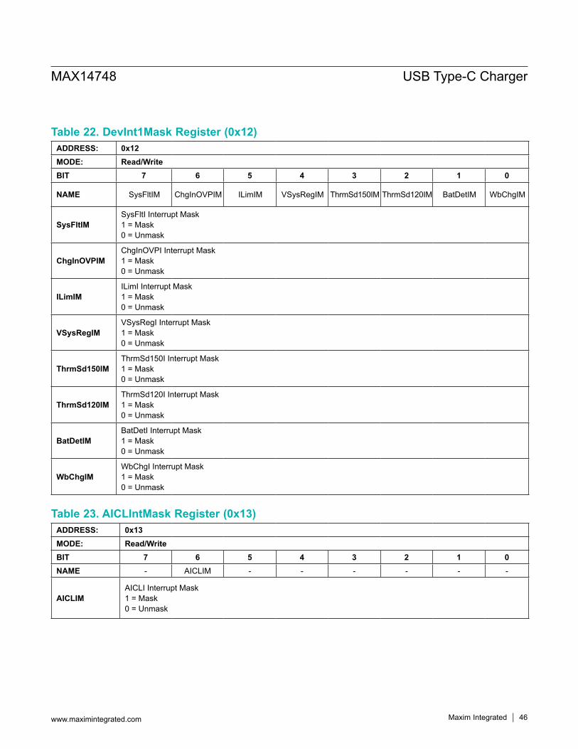
Table 23. AICLIntMask Register (0x13)
Table 22. DevInt1Mask Register (0x12)ADDRESS: 0x12MODE: Read/WriteBIT 7 6 5 4 3 2 1 0
NAME SysFltIM ChgInOVPIM ILimIM VSysRegIM ThrmSd150IM ThrmSd120IM BatDetIM WbChgIM
SysFltIMSysFltI Interrupt Mask1 = Mask 0 = Unmask
ChgInOVPIMChgInOVPI Interrupt Mask1 = Mask 0 = Unmask
ILimIMILimI Interrupt Mask1 = Mask 0 = Unmask
VSysRegIMVSysRegI Interrupt Mask1 = Mask 0 = Unmask
ThrmSd150IMThrmSd150I Interrupt Mask1 = Mask 0 = Unmask
ThrmSd120IMThrmSd120I Interrupt Mask1 = Mask 0 = Unmask
BatDetIMBatDetI Interrupt Mask1 = Mask 0 = Unmask
WbChgIMWbChgI Interrupt Mask1 = Mask 0 = Unmask
ADDRESS: 0x13MODE: Read/WriteBIT 7 6 5 4 3 2 1 0NAME - AICLIM - - - - - -
AICLIMAICLI Interrupt Mask1 = Mask 0 = Unmask
MAX14748 USB Type-C Charger
www.maximintegrated.com Maxim Integrated │ 46
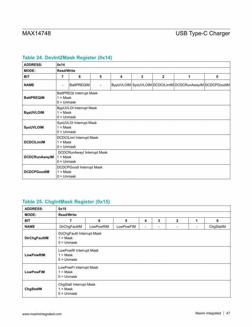
Table 25. ChgIntMask Register (0x15)
Table 24. DevInt2Mask Register (0x14)ADDRESS: 0x14MODE: Read/WriteBIT 7 6 5 4 3 2 1 0
NAME - BattPREQIM - BypUVLOIM SysUVLOIM DCDCILimIM DCDCRunAwayIM DCDCPGoodIM
BattPREQIMBattPREQI Interrupt Mask1 = Mask 0 = Unmask
BypUVLOIMBypUVLOI Interrupt Mask1 = Mask 0 = Unmask
SysUVLOIMSysUVLOI Interrupt Mask1 = Mask 0 = Unmask
DCDCILimIMDCDCILimI Interrupt Mask1 = Mask0 = Unmask
DCDCRunAwayIM DCDCRunAwayI Interrupt Mask1 = Mask0 = Unmask
DCDCPGoodIMDCDCPGoodI Interrupt Mask1 = Mask 0 = Unmask
ADDRESS: 0x15MODE: Read/WriteBIT 7 6 5 4 3 2 1 0NAME DirChgFaultIM LowPowRIM LowPowFIM - - - - ChgStatIM
DirChgFaultIMDirChgFaultI Interrupt Mask1 = Mask 0 = Unmask
LowPowRIMLowPowRI Interrupt Mask1 = Mask 0 = Unmask
LowPowFIMLowPowFI Interrupt Mask1 = Mask 0 = Unmask
ChgStatIMChgStatI Interrupt Mask1 = Mask 0 = Unmask
MAX14748 USB Type-C Charger
www.maximintegrated.com Maxim Integrated │ 47
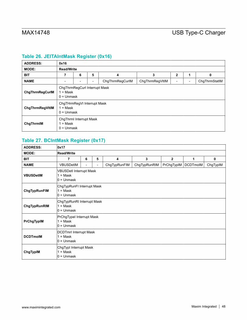
Table 27. BCIntMask Register (0x17)
Table 26. JEITAIntMask Register (0x16)ADDRESS: 0x16MODE: Read/WriteBIT 7 6 5 4 3 2 1 0NAME - - - ChgThrmRegCurIM ChgThrmRegVltIM - - ChgThrmStatIM
ChgThrmRegCurIMChgThrmRegCurI Interrupt Mask1 = Mask 0 = Unmask
ChgThrmRegVltIMChgTHrmRegVI Interrupt Mask1 = Mask 0 = Unmask
ChgThrmIMChgThrmI Interrupt Mask1 = Mask 0 = Unmask
ADDRESS: 0x17MODE: Read/WriteBIT 7 6 5 4 3 2 1 0NAME VBUSDetIM - - ChgTypRunFIM ChgTypRunRIM PrChgTypIM DCDTmoIM ChgTypIM
VBUSDetIMVBUSDetI Interrupt Mask1 = Mask 0 = Unmask
ChgTypRunFIMChgTypRunFI Interrupt Mask1 = Mask 0 = Unmask
ChgTypRunRIMChgTypRunRI Interrupt Mask1 = Mask 0 = Unmask
PrChgTypIMPrChgTypeI Interrupt Mask1 = Mask 0 = Unmask
DCDTmoIMDCDTmrI Interrupt Mask1 = Mask 0 = Unmask
ChgTypIMChgTypI Interrupt Mask1 = Mask 0 = Unmask
MAX14748 USB Type-C Charger
www.maximintegrated.com Maxim Integrated │ 48
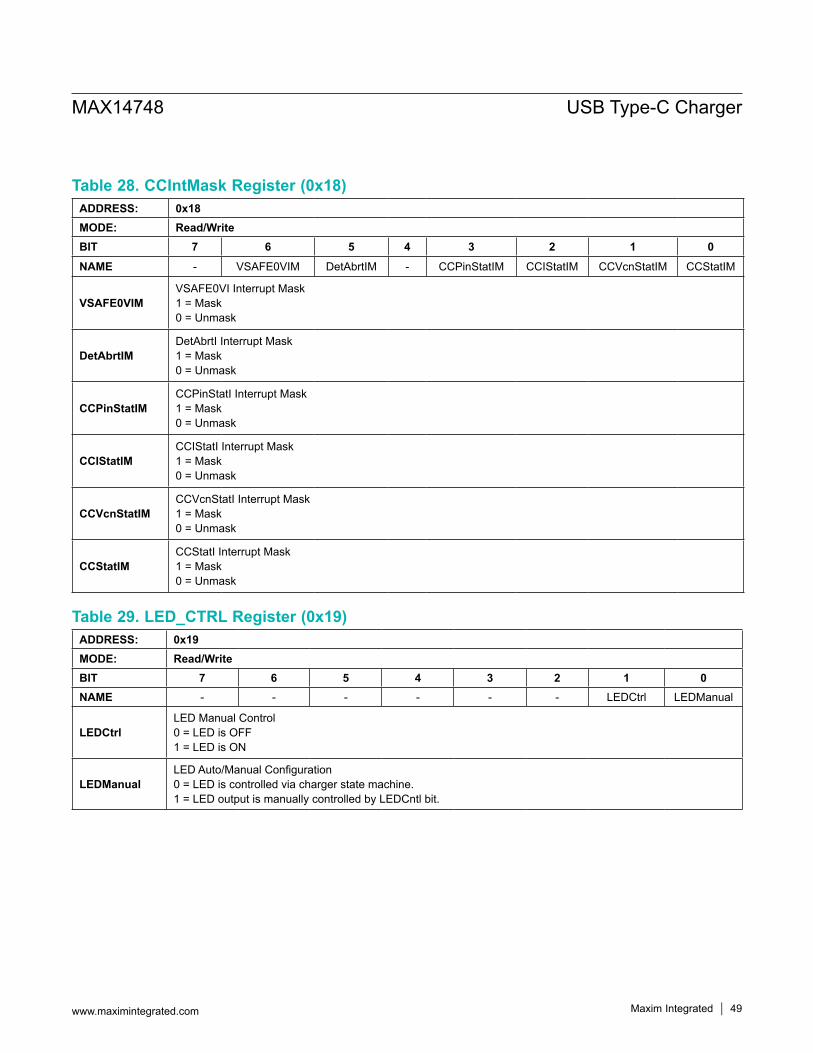
Table 29. LED_CTRL Register (0x19)
Table 28. CCIntMask Register (0x18)ADDRESS: 0x18MODE: Read/WriteBIT 7 6 5 4 3 2 1 0NAME - VSAFE0VIM DetAbrtIM - CCPinStatIM CCIStatIM CCVcnStatIM CCStatIM
VSAFE0VIMVSAFE0VI Interrupt Mask1 = Mask 0 = Unmask
DetAbrtIMDetAbrtI Interrupt Mask1 = Mask 0 = Unmask
CCPinStatIMCCPinStatI Interrupt Mask1 = Mask 0 = Unmask
CCIStatIMCCIStatI Interrupt Mask1 = Mask 0 = Unmask
CCVcnStatIMCCVcnStatI Interrupt Mask1 = Mask 0 = Unmask
CCStatIMCCStatI Interrupt Mask1 = Mask 0 = Unmask
ADDRESS: 0x19MODE: Read/WriteBIT 7 6 5 4 3 2 1 0NAME - - - - - - LEDCtrl LEDManual
LEDCtrlLED Manual Control 0 = LED is OFF 1 = LED is ON
LEDManualLED Auto/Manual Configuration 0 = LED is controlled via charger state machine. 1 = LED output is manually controlled by LEDCntl bit.
MAX14748 USB Type-C Charger
www.maximintegrated.com Maxim Integrated │ 49
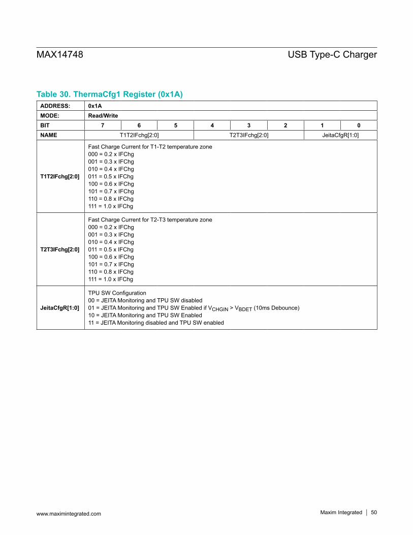
Table 30. ThermaCfg1 Register (0x1A)ADDRESS: 0x1AMODE: Read/WriteBIT 7 6 5 4 3 2 1 0NAME T1T2IFchg[2:0] T2T3IFchg[2:0] JeitaCfgR[1:0]
T1T2IFchg[2:0]
Fast Charge Current for T1-T2 temperature zone 000 = 0.2 x IFChg 001 = 0.3 x IFChg 010 = 0.4 x IFChg 011 = 0.5 x IFChg 100 = 0.6 x IFChg 101 = 0.7 x IFChg 110 = 0.8 x IFChg 111 = 1.0 x IFChg
T2T3IFchg[2:0]
Fast Charge Current for T2-T3 temperature zone 000 = 0.2 x IFChg 001 = 0.3 x IFChg 010 = 0.4 x IFChg 011 = 0.5 x IFChg 100 = 0.6 x IFChg 101 = 0.7 x IFChg 110 = 0.8 x IFChg 111 = 1.0 x IFChg
JeitaCfgR[1:0]
TPU SW Configuration00 = JEITA Monitoring and TPU SW disabled 01 = JEITA Monitoring and TPU SW Enabled if VCHGIN > VBDET (10ms Debounce)10 = JEITA Monitoring and TPU SW Enabled11 = JEITA Monitoring disabled and TPU SW enabled
MAX14748 USB Type-C Charger
www.maximintegrated.com Maxim Integrated │ 50
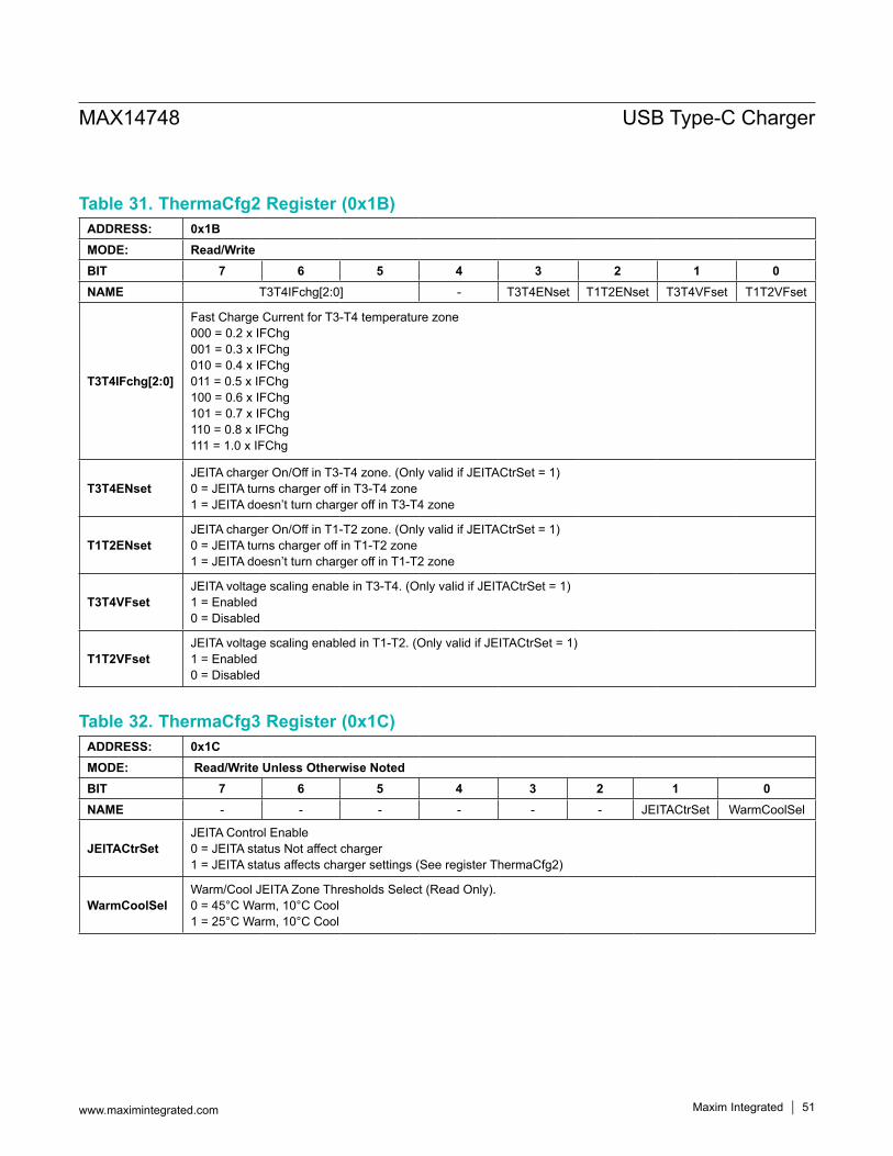
Table 32. ThermaCfg3 Register (0x1C)
Table 31. ThermaCfg2 Register (0x1B)ADDRESS: 0x1BMODE: Read/WriteBIT 7 6 5 4 3 2 1 0NAME T3T4IFchg[2:0] - T3T4ENset T1T2ENset T3T4VFset T1T2VFset
T3T4IFchg[2:0]
Fast Charge Current for T3-T4 temperature zone 000 = 0.2 x IFChg 001 = 0.3 x IFChg 010 = 0.4 x IFChg 011 = 0.5 x IFChg 100 = 0.6 x IFChg 101 = 0.7 x IFChg 110 = 0.8 x IFChg 111 = 1.0 x IFChg
T3T4ENsetJEITA charger On/Off in T3-T4 zone. (Only valid if JEITACtrSet = 1)0 = JEITA turns charger off in T3-T4 zone 1 = JEITA doesn’t turn charger off in T3-T4 zone
T1T2ENsetJEITA charger On/Off in T1-T2 zone. (Only valid if JEITACtrSet = 1)0 = JEITA turns charger off in T1-T2 zone 1 = JEITA doesn’t turn charger off in T1-T2 zone
T3T4VFsetJEITA voltage scaling enable in T3-T4. (Only valid if JEITACtrSet = 1) 1 = Enabled 0 = Disabled
T1T2VFsetJEITA voltage scaling enabled in T1-T2. (Only valid if JEITACtrSet = 1) 1 = Enabled 0 = Disabled
ADDRESS: 0x1CMODE: Read/Write Unless Otherwise NotedBIT 7 6 5 4 3 2 1 0NAME - - - - - - JEITACtrSet WarmCoolSel
JEITACtrSetJEITA Control Enable0 = JEITA status Not affect charger1 = JEITA status affects charger settings (See register ThermaCfg2)
WarmCoolSelWarm/Cool JEITA Zone Thresholds Select (Read Only). 0 = 45°C Warm, 10°C Cool 1 = 25°C Warm, 10°C Cool
MAX14748 USB Type-C Charger
www.maximintegrated.com Maxim Integrated │ 51
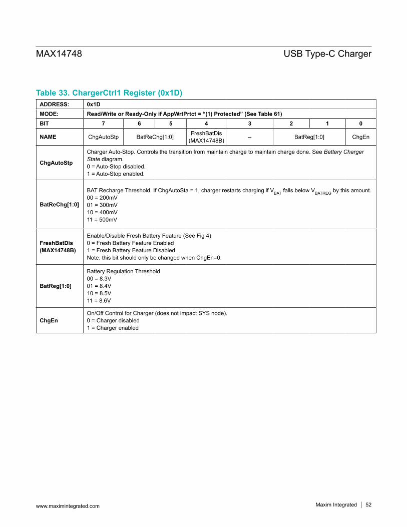
Table 33. ChargerCtrl1 Register (0x1D)ADDRESS: 0x1DMODE: Read/Write or Ready-Only if AppWrtPrtct = “(1) Protected” (See Table 61) BIT 7 6 5 4 3 2 1 0
NAME ChgAutoStp BatReChg[1:0] FreshBatDis (MAX14748B) – BatReg[1:0] ChgEn
ChgAutoStp
Charger Auto-Stop. Controls the transition from maintain charge to maintain charge done. See Battery Charger State diagram. 0 = Auto-Stop disabled. 1 = Auto-Stop enabled.
BatReChg[1:0]
BAT Recharge Threshold. If ChgAutoSta = 1, charger restarts charging if VBAT falls below VBATREG by this amount.00 = 200mV 01 = 300mV 10 = 400mV 11 = 500mV
FreshBatDis (MAX14748B)
Enable/Disable Fresh Battery Feature (See Fig 4)0 = Fresh Battery Feature Enabled1 = Fresh Battery Feature DisabledNote, this bit should only be changed when ChgEn=0.
BatReg[1:0]
Battery Regulation Threshold 00 = 8.3V 01 = 8.4V 10 = 8.5V 11 = 8.6V
ChgEn On/Off Control for Charger (does not impact SYS node). 0 = Charger disabled 1 = Charger enabled
MAX14748 USB Type-C Charger
www.maximintegrated.com Maxim Integrated │ 52
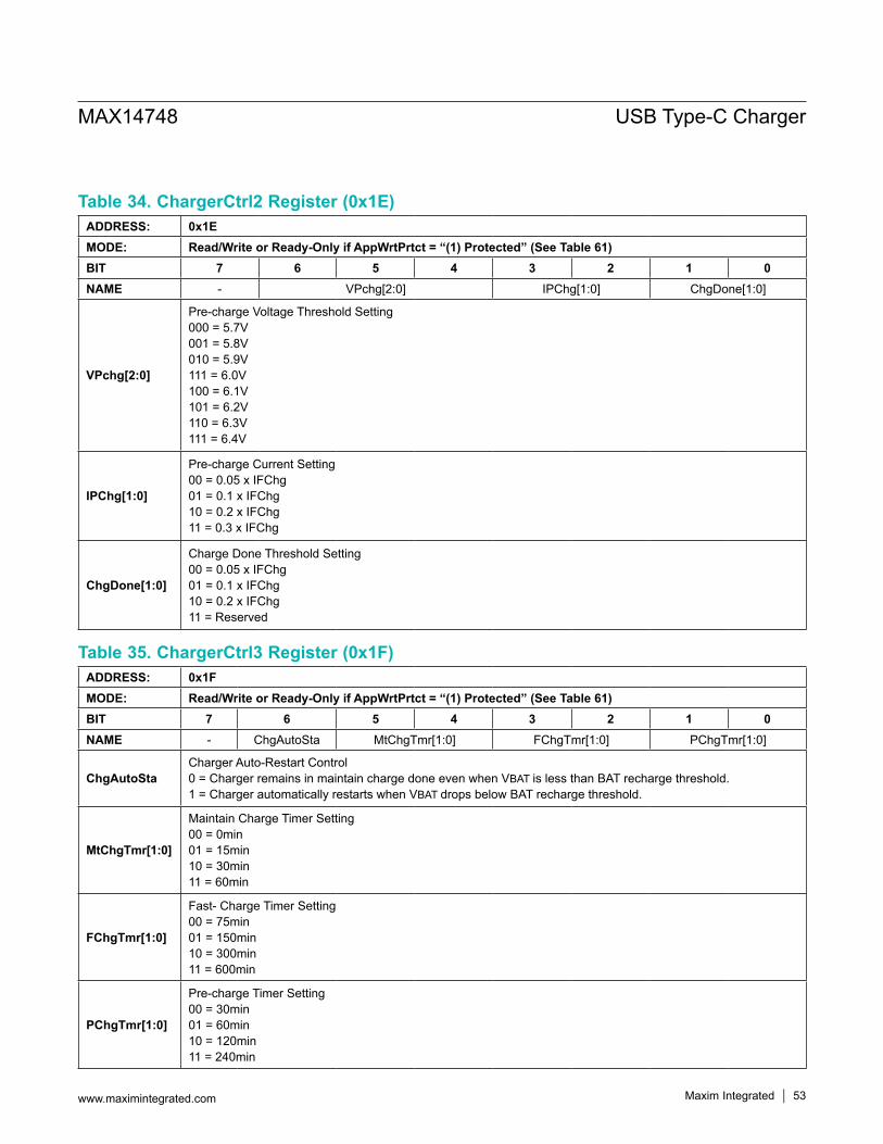
Table 35. ChargerCtrl3 Register (0x1F)
Table 34. ChargerCtrl2 Register (0x1E)ADDRESS: 0x1EMODE: Read/Write or Ready-Only if AppWrtPrtct = “(1) Protected” (See Table 61) BIT 7 6 5 4 3 2 1 0NAME - VPchg[2:0] IPChg[1:0] ChgDone[1:0]
VPchg[2:0]
Pre-charge Voltage Threshold Setting 000 = 5.7V 001 = 5.8V 010 = 5.9V 111 = 6.0V 100 = 6.1V 101 = 6.2V 110 = 6.3V 111 = 6.4V
IPChg[1:0]
Pre-charge Current Setting 00 = 0.05 x IFChg 01 = 0.1 x IFChg 10 = 0.2 x IFChg 11 = 0.3 x IFChg
ChgDone[1:0]
Charge Done Threshold Setting 00 = 0.05 x IFChg 01 = 0.1 x IFChg 10 = 0.2 x IFChg 11 = Reserved
ADDRESS: 0x1FMODE: Read/Write or Ready-Only if AppWrtPrtct = “(1) Protected” (See Table 61)BIT 7 6 5 4 3 2 1 0NAME - ChgAutoSta MtChgTmr[1:0] FChgTmr[1:0] PChgTmr[1:0]
ChgAutoStaCharger Auto-Restart Control0 = Charger remains in maintain charge done even when VBAT is less than BAT recharge threshold.1 = Charger automatically restarts when VBAT drops below BAT recharge threshold.
MtChgTmr[1:0]
Maintain Charge Timer Setting 00 = 0min 01 = 15min 10 = 30min 11 = 60min
FChgTmr[1:0]
Fast- Charge Timer Setting 00 = 75min 01 = 150min 10 = 300min 11 = 600min
PChgTmr[1:0]
Pre-charge Timer Setting 00 = 30min 01 = 60min 10 = 120min 11 = 240min
MAX14748 USB Type-C Charger
www.maximintegrated.com Maxim Integrated │ 53
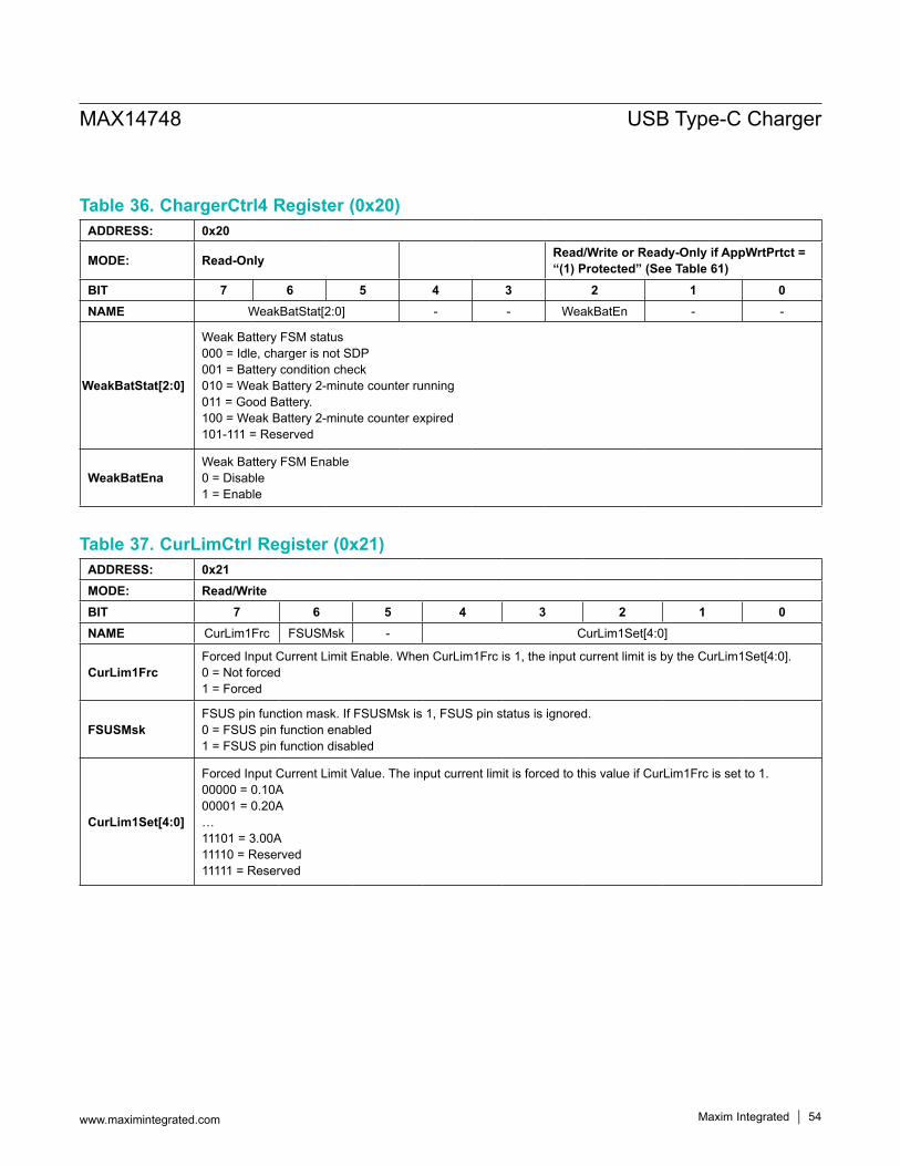
Table 37. CurLimCtrl Register (0x21)
Table 36. ChargerCtrl4 Register (0x20)ADDRESS: 0x20
MODE: Read-Only Read/Write or Ready-Only if AppWrtPrtct = “(1) Protected” (See Table 61)
BIT 7 6 5 4 3 2 1 0NAME WeakBatStat[2:0] - - WeakBatEn - -
WeakBatStat[2:0]
Weak Battery FSM status 000 = Idle, charger is not SDP 001 = Battery condition check 010 = Weak Battery 2-minute counter running 011 = Good Battery. 100 = Weak Battery 2-minute counter expired101-111 = Reserved
WeakBatEnaWeak Battery FSM Enable 0 = Disable 1 = Enable
ADDRESS: 0x21MODE: Read/WriteBIT 7 6 5 4 3 2 1 0NAME CurLim1Frc FSUSMsk - CurLim1Set[4:0]
CurLim1FrcForced Input Current Limit Enable. When CurLim1Frc is 1, the input current limit is by the CurLim1Set[4:0]. 0 = Not forced1 = Forced
FSUSMskFSUS pin function mask. If FSUSMsk is 1, FSUS pin status is ignored. 0 = FSUS pin function enabled1 = FSUS pin function disabled
CurLim1Set[4:0]
Forced Input Current Limit Value. The input current limit is forced to this value if CurLim1Frc is set to 1.00000 = 0.10A 00001 = 0.20A …11101 = 3.00A11110 = Reserved11111 = Reserved
MAX14748 USB Type-C Charger
www.maximintegrated.com Maxim Integrated │ 54
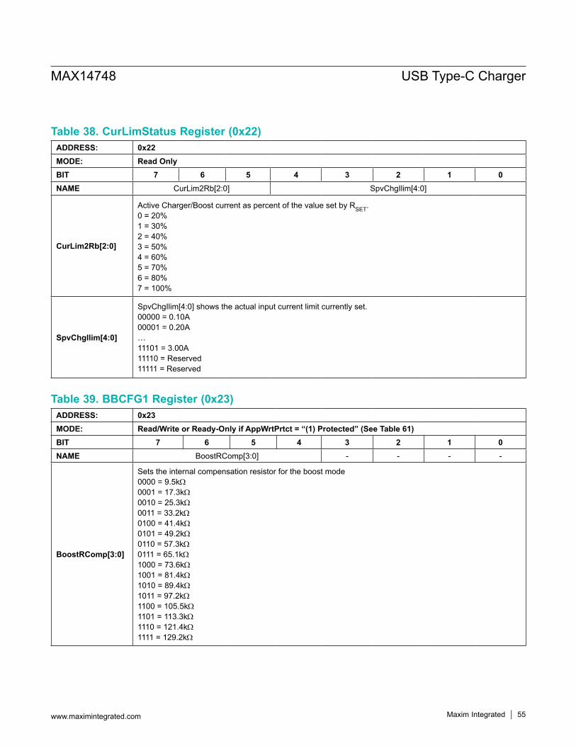
Table 39. BBCFG1 Register (0x23)
Table 38. CurLimStatus Register (0x22)ADDRESS: 0x22MODE: Read OnlyBIT 7 6 5 4 3 2 1 0NAME CurLim2Rb[2:0] SpvChgIlim[4:0]
CurLim2Rb[2:0]
Active Charger/Boost current as percent of the value set by RSET. 0 = 20% 1 = 30% 2 = 40% 3 = 50% 4 = 60% 5 = 70% 6 = 80% 7 = 100%
SpvChgIlim[4:0]
SpvChgIlim[4:0] shows the actual input current limit currently set. 00000 = 0.10A 00001 = 0.20A …11101 = 3.00A11110 = Reserved11111 = Reserved
ADDRESS: 0x23MODE: Read/Write or Ready-Only if AppWrtPrtct = “(1) Protected” (See Table 61)BIT 7 6 5 4 3 2 1 0NAME BoostRComp[3:0] - - - -
BoostRComp[3:0]
Sets the internal compensation resistor for the boost mode 0000 = 9.5kW 0001 = 17.3kW 0010 = 25.3kW 0011 = 33.2kW 0100 = 41.4kW 0101 = 49.2kW 0110 = 57.3kW 0111 = 65.1kW 1000 = 73.6kW 1001 = 81.4kW 1010 = 89.4kW 1011 = 97.2kW 1100 = 105.5kW 1101 = 113.3kW 1110 = 121.4kW 1111 = 129.2kW
MAX14748 USB Type-C Charger
www.maximintegrated.com Maxim Integrated │ 55
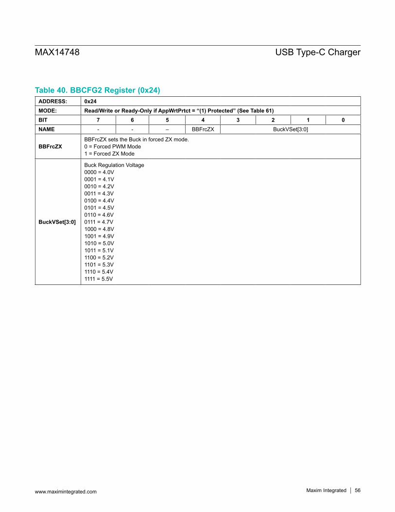
Table 40. BBCFG2 Register (0x24)ADDRESS: 0x24MODE: Read/Write or Ready-Only if AppWrtPrtct = “(1) Protected” (See Table 61)BIT 7 6 5 4 3 2 1 0NAME - - – BBFrcZX BuckVSet[3:0]
BBFrcZXBBFrcZX sets the Buck in forced ZX mode.0 = Forced PWM Mode1 = Forced ZX Mode
BuckVSet[3:0]
Buck Regulation Voltage 0000 = 4.0V 0001 = 4.1V 0010 = 4.2V 0011 = 4.3V 0100 = 4.4V 0101 = 4.5V 0110 = 4.6V 0111 = 4.7V 1000 = 4.8V 1001 = 4.9V 1010 = 5.0V 1011 = 5.1V 1100 = 5.2V 1101 = 5.3V 1110 = 5.4V 1111 = 5.5V
MAX14748 USB Type-C Charger
www.maximintegrated.com Maxim Integrated │ 56
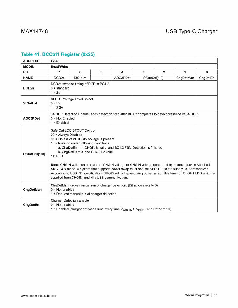
Table 41. BCCtrl1 Register (0x25)ADDRESS: 0x25MODE: Read/WriteBIT 7 6 5 4 3 2 1 0NAME DCD2s SfOutLvl - ADC3PDet SfOutCtrl[1:0] ChgDetMan ChgDetEn
DCD2sDCD2s sets the timing of DCD in BC1.2 0 = standard 1 = 2s
SfOutLvlSFOUT Voltage Level Select 0 = 5V 1 = 3.3V
ADC3PDet3A DCP Detection Enable (adds detection step after BC1.2 completes to detect presence of 3A DCP) 0 = Not Enabled 1 = Enabled
SfOutCtrl[1:0]
Safe Out LDO SFOUT Control 00 = Always Disabled 01 = On if a valid CHGIN voltage is present 10 =Turns on under following conditions. a. ChgDetEn = 1, CHGIN is valid, and BC1.2 FSM Detection is finished b. ChgDetEn = 0, and CHGIN is valid 11: RFU Note: CHGIN valid can be external CHGIN voltage or CHGIN voltage generated by reverse buck in Attached.SRC_CCx mode. A system that supports power swap must not use SFOUT LDO to supply USB transceiver. According to USB PD specification, CHGIN will collapse during power swap. This turns off SFOUT LDO which is supplied from CHGIN, and kills USB communication.
ChgDetManChgDetMan forces manual run of charger detection. (Bit auto-resets to 0) 0 = Not enabled 1 = Request manual run of charger detection
ChgDetEnCharger Detection Enable 0 = Not enabled 1 = Enabled (charger detection runs every time VCHGIN > VBDET and DetAbrt = 0)
MAX14748 USB Type-C Charger
www.maximintegrated.com Maxim Integrated │ 57
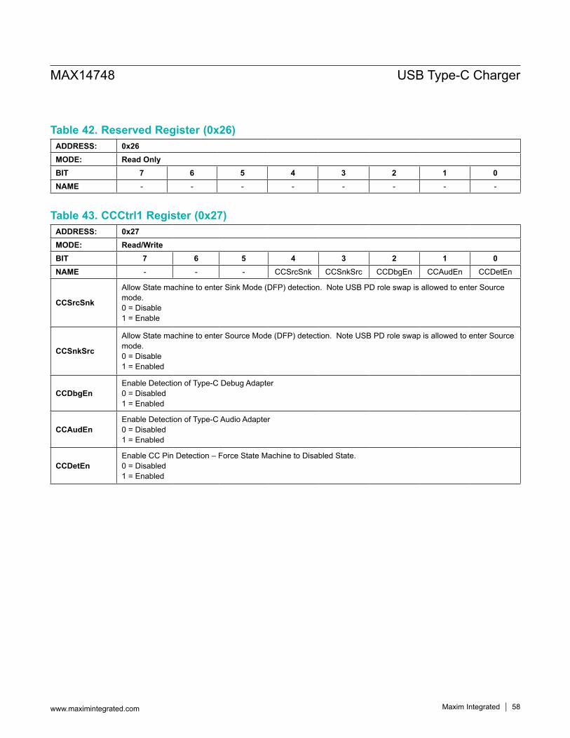
Table 43. CCCtrl1 Register (0x27)
Table 42. Reserved Register (0x26)
ADDRESS: 0x27MODE: Read/WriteBIT 7 6 5 4 3 2 1 0NAME - - - CCSrcSnk CCSnkSrc CCDbgEn CCAudEn CCDetEn
CCSrcSnk
Allow State machine to enter Sink Mode (DFP) detection. Note USB PD role swap is allowed to enter Source mode.0 = Disable1 = Enable
CCSnkSrc
Allow State machine to enter Source Mode (DFP) detection. Note USB PD role swap is allowed to enter Source mode. 0 = Disable 1 = Enabled
CCDbgEnEnable Detection of Type-C Debug Adapter 0 = Disabled 1 = Enabled
CCAudEnEnable Detection of Type-C Audio Adapter 0 = Disabled 1 = Enabled
CCDetEnEnable CC Pin Detection – Force State Machine to Disabled State. 0 = Disabled 1 = Enabled
ADDRESS: 0x26MODE: Read OnlyBIT 7 6 5 4 3 2 1 0NAME - - - - - - - -
MAX14748 USB Type-C Charger
www.maximintegrated.com Maxim Integrated │ 58
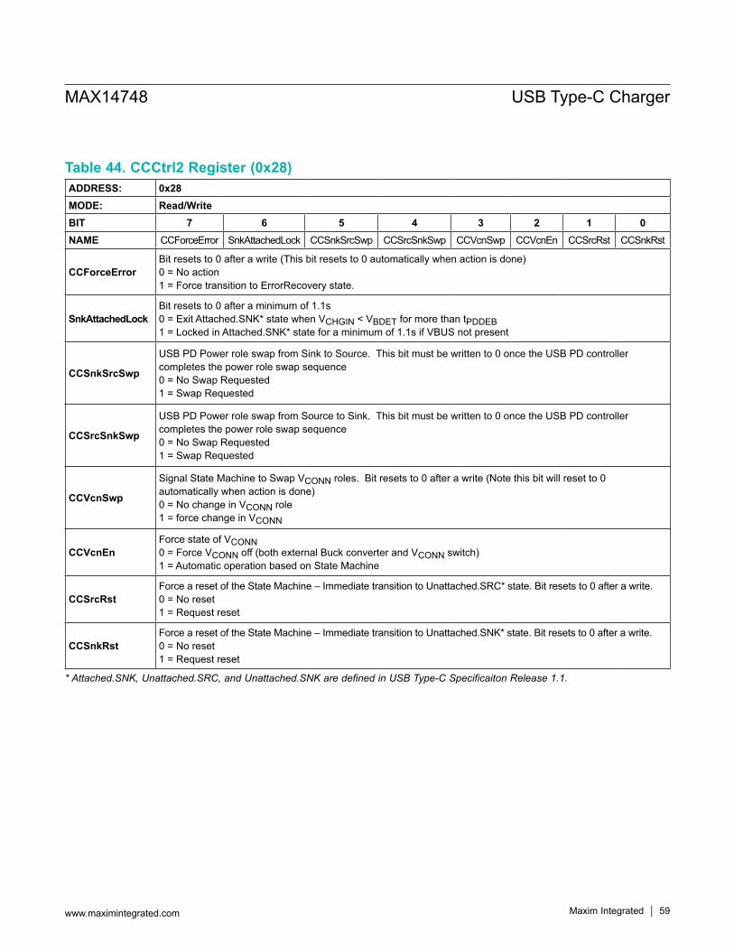
Table 44. CCCtrl2 Register (0x28)
* Attached.SNK, Unattached.SRC, and Unattached.SNK are defined in USB Type-C Specificaiton Release 1.1.
ADDRESS: 0x28MODE: Read/WriteBIT 7 6 5 4 3 2 1 0NAME CCForceError SnkAttachedLock CCSnkSrcSwp CCSrcSnkSwp CCVcnSwp CCVcnEn CCSrcRst CCSnkRst
CCForceErrorBit resets to 0 after a write (This bit resets to 0 automatically when action is done) 0 = No action 1 = Force transition to ErrorRecovery state.
SnkAttachedLockBit resets to 0 after a minimum of 1.1s 0 = Exit Attached.SNK* state when VCHGIN < VBDET for more than tPDDEB 1 = Locked in Attached.SNK* state for a minimum of 1.1s if VBUS not present
CCSnkSrcSwp
USB PD Power role swap from Sink to Source. This bit must be written to 0 once the USB PD controller completes the power role swap sequence 0 = No Swap Requested 1 = Swap Requested
CCSrcSnkSwp
USB PD Power role swap from Source to Sink. This bit must be written to 0 once the USB PD controller completes the power role swap sequence 0 = No Swap Requested 1 = Swap Requested
CCVcnSwp
Signal State Machine to Swap VCONN roles. Bit resets to 0 after a write (Note this bit will reset to 0 automatically when action is done) 0 = No change in VCONN role 1 = force change in VCONN
CCVcnEnForce state of VCONN 0 = Force VCONN off (both external Buck converter and VCONN switch) 1 = Automatic operation based on State Machine
CCSrcRstForce a reset of the State Machine – Immediate transition to Unattached.SRC* state. Bit resets to 0 after a write. 0 = No reset 1 = Request reset
CCSnkRstForce a reset of the State Machine – Immediate transition to Unattached.SNK* state. Bit resets to 0 after a write. 0 = No reset 1 = Request reset
MAX14748 USB Type-C Charger
www.maximintegrated.com Maxim Integrated │ 59
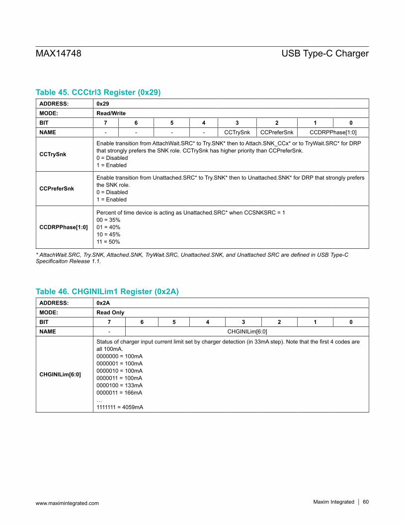
Table 46. CHGINILim1 Register (0x2A)
Table 45. CCCtrl3 Register (0x29)
* AttachWait.SRC, Try.SNK, Attached.SNK, TryWait.SRC, Unattached.SNK, and Unattached SRC are defined in USB Type-C Specificaiton Release 1.1.
ADDRESS: 0x29MODE: Read/WriteBIT 7 6 5 4 3 2 1 0NAME - - - - CCTrySnk CCPreferSnk CCDRPPhase[1:0]
CCTrySnk
Enable transition from AttachWait.SRC* to Try.SNK* then to Attach.SNK_CCx* or to TryWait.SRC* for DRP that strongly prefers the SNK role. CCTrySnk has higher priority than CCPreferSnk. 0 = Disabled1 = Enabled
CCPreferSnk
Enable transition from Unattached.SRC* to Try.SNK* then to Unattached.SNK* for DRP that strongly prefers the SNK role.0 = Disabled1 = Enabled
CCDRPPhase[1:0]
Percent of time device is acting as Unattached.SRC* when CCSNKSRC = 1 00 = 35% 01 = 40% 10 = 45% 11 = 50%
ADDRESS: 0x2AMODE: Read OnlyBIT 7 6 5 4 3 2 1 0NAME - CHGINILim[6:0]
CHGINILim[6:0]
Status of charger input current limit set by charger detection (in 33mA step). Note that the first 4 codes are all 100mA. 0000000 = 100mA0000001 = 100mA0000010 = 100mA0000011 = 100mA0000100 = 133mA0000011 = 166mA…1111111 = 4059mA
MAX14748 USB Type-C Charger
www.maximintegrated.com Maxim Integrated │ 60
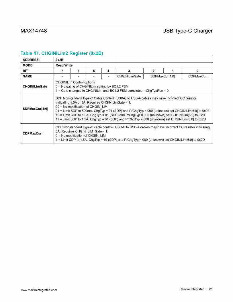
Table 47. CHGINILim2 Register (0x2B)ADDRESS: 0x2BMODE: Read/WriteBIT 7 6 5 4 3 2 1 0NAME - - - - CHGINILimGate SDPMaxCur[1:0] CDPMaxCur
CHGINILimGateCHGINILim Control options 0 = No gating of CHGINILim setting by BC1.2 FSM 1 = Gate changes in CHGINILim until BC1.2 FSM completes – ChgTypRun = 0
SDPMaxCur[1:0]
SDP Nonstandard Type-C Cable Control. USB-C to USB-A cables may have incorrect CC resistor indicating 1.5A or 3A. Requires CHGINILimGate = 1. 00 = No modification of CHGIN_LIM 01 = Limit SDP to 500mA. ChgTyp = 01 (SDP) and PrChgTyp = 000 (unknown) set CHGINILim[6:0] to 0x0F 10 = Limit SDP to 1.0A. ChgTyp = 01 (SDP) and PrChgTyp = 000 (unknown) set CHGINILim[6:0] to 0x1E 11 = Limit SDP to 1.5A. ChgTyp = 01 (SDP) and PrChgTyp = 000 (unknown) set CHGINILim[6:0] to 0x2D
CDPMaxCur
CDP Nonstandard Type-C cable control. USB-C to USB-A cables may have incorrect CC resistor indicating 3A. Requires CHGIN_LIM_Gate = 1. 0 = No modification of CHGIN_LIM 1 = Limit CDP to 1.5A. ChgTyp = 10 (CDP) and PrChgTyp = 000 (unknown) set CHGINILim[6:0] to 0x2D
MAX14748 USB Type-C Charger
www.maximintegrated.com Maxim Integrated │ 61
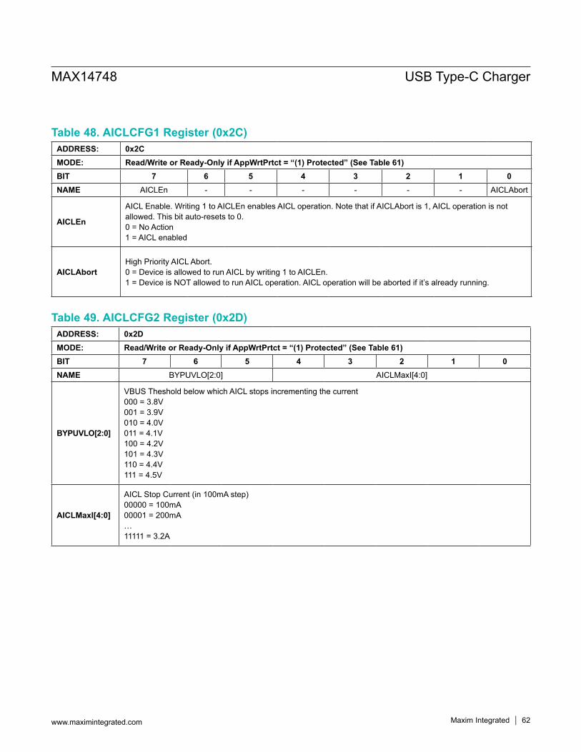
Table 49. AICLCFG2 Register (0x2D)
Table 48. AICLCFG1 Register (0x2C)ADDRESS: 0x2CMODE: Read/Write or Ready-Only if AppWrtPrtct = “(1) Protected” (See Table 61)BIT 7 6 5 4 3 2 1 0NAME AICLEn - - - - - - AICLAbort
AICLEn
AICL Enable. Writing 1 to AICLEn enables AICL operation. Note that if AICLAbort is 1, AICL operation is not allowed. This bit auto-resets to 0. 0 = No Action 1 = AICL enabled
AICLAbortHigh Priority AICL Abort. 0 = Device is allowed to run AICL by writing 1 to AICLEn. 1 = Device is NOT allowed to run AICL operation. AICL operation will be aborted if it’s already running.
ADDRESS: 0x2DMODE: Read/Write or Ready-Only if AppWrtPrtct = “(1) Protected” (See Table 61)BIT 7 6 5 4 3 2 1 0NAME BYPUVLO[2:0] AICLMaxI[4:0]
BYPUVLO[2:0]
VBUS Theshold below which AICL stops incrementing the current 000 = 3.8V 001 = 3.9V 010 = 4.0V 011 = 4.1V 100 = 4.2V 101 = 4.3V 110 = 4.4V 111 = 4.5V
AICLMaxI[4:0]
AICL Stop Current (in 100mA step)00000 = 100mA00001 = 200mA…11111 = 3.2A
MAX14748 USB Type-C Charger
www.maximintegrated.com Maxim Integrated │ 62
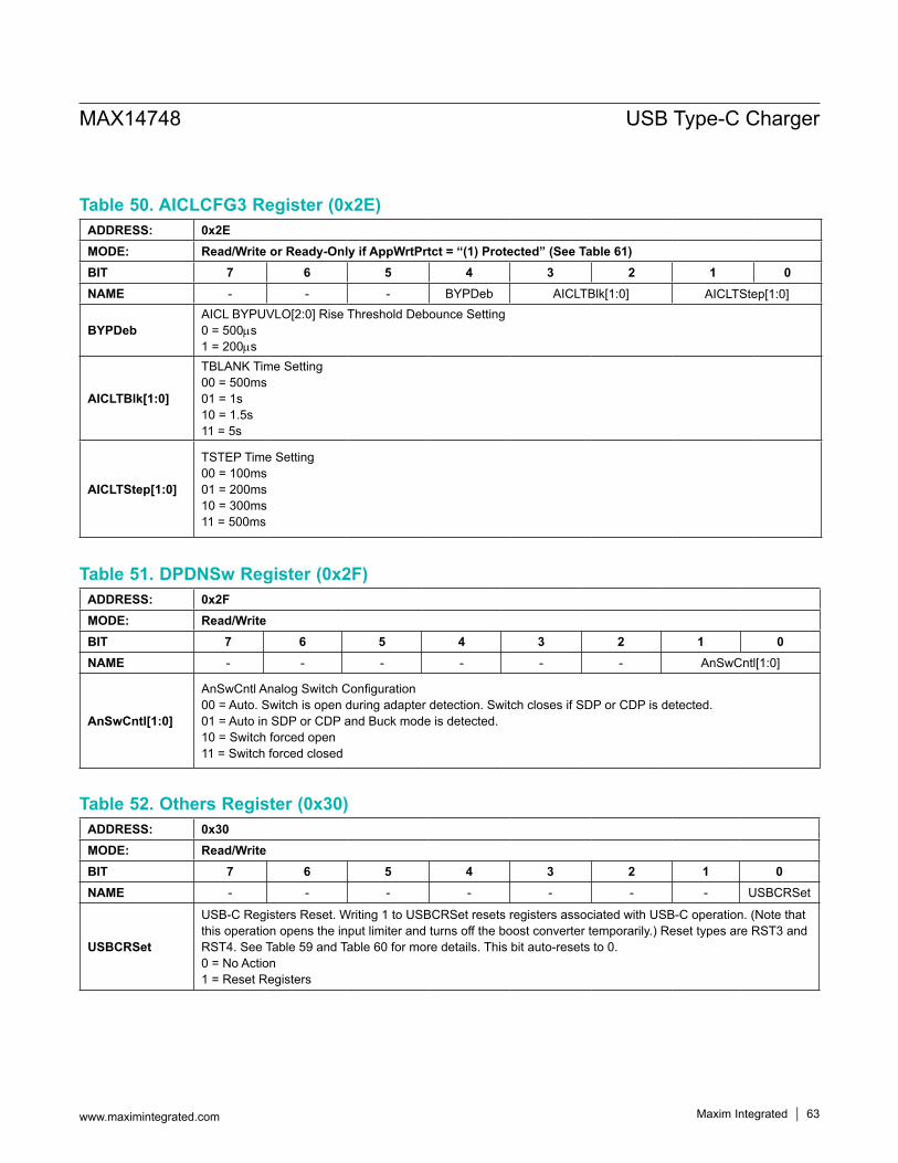
Table 52. Others Register (0x30)
Table 51. DPDNSw Register (0x2F)
Table 50. AICLCFG3 Register (0x2E)ADDRESS: 0x2EMODE: Read/Write or Ready-Only if AppWrtPrtct = “(1) Protected” (See Table 61)BIT 7 6 5 4 3 2 1 0NAME - - - BYPDeb AICLTBlk[1:0] AICLTStep[1:0]
BYPDebAICL BYPUVLO[2:0] Rise Threshold Debounce Setting0 = 500ms1 = 200ms
AICLTBlk[1:0]
TBLANK Time Setting 00 = 500ms01 = 1s 10 = 1.5s11 = 5s
AICLTStep[1:0]
TSTEP Time Setting 00 = 100ms 01 = 200ms 10 = 300ms 11 = 500ms
ADDRESS: 0x2FMODE: Read/WriteBIT 7 6 5 4 3 2 1 0NAME - - - - - - AnSwCntl[1:0]
AnSwCntl[1:0]
AnSwCntl Analog Switch Configuration 00 = Auto. Switch is open during adapter detection. Switch closes if SDP or CDP is detected. 01 = Auto in SDP or CDP and Buck mode is detected. 10 = Switch forced open 11 = Switch forced closed
ADDRESS: 0x30MODE: Read/WriteBIT 7 6 5 4 3 2 1 0NAME - - - - - - - USBCRSet
USBCRSet
USB-C Registers Reset. Writing 1 to USBCRSet resets registers associated with USB-C operation. (Note that this operation opens the input limiter and turns off the boost converter temporarily.) Reset types are RST3 and RST4. See Table 59 and Table 60 for more details. This bit auto-resets to 0.0 = No Action1 = Reset Registers
MAX14748 USB Type-C Charger
www.maximintegrated.com Maxim Integrated │ 63
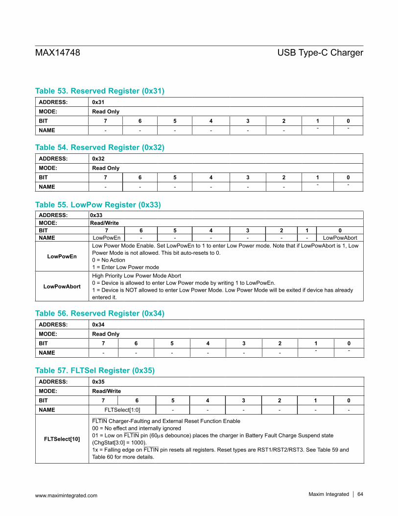
Table 57. FLTSel Register (0x35)
Table 56. Reserved Register (0x34)
Table 55. LowPow Register (0x33)
Table 54. Reserved Register (0x32)
Table 53. Reserved Register (0x31)ADDRESS: 0x31MODE: Read OnlyBIT 7 6 5 4 3 2 1 0NAME - - - - - - - -
ADDRESS: 0x32MODE: Read OnlyBIT 7 6 5 4 3 2 1 0NAME - - - - - - - -
ADDRESS: 0x33MODE: Read/WriteBIT 7 6 5 4 3 2 1 0NAME LowPowEn - - - - - - LowPowAbort
LowPowEn
Low Power Mode Enable. Set LowPowEn to 1 to enter Low Power mode. Note that if LowPowAbort is 1, Low Power Mode is not allowed. This bit auto-resets to 0.0 = No Action1 = Enter Low Power mode
LowPowAbort
High Priority Low Power Mode Abort0 = Device is allowed to enter Low Power mode by writing 1 to LowPowEn.1 = Device is NOT allowed to enter Low Power Mode. Low Power Mode will be exited if device has already entered it.
ADDRESS: 0x34MODE: Read OnlyBIT 7 6 5 4 3 2 1 0NAME - - - - - - - -
ADDRESS: 0x35MODE: Read/WriteBIT 7 6 5 4 3 2 1 0NAME FLTSelect[1:0] - - - - - -
FLTSelect[10]
FLTIN Charger-Faulting and External Reset Function Enable00 = No effect and internally ignored 01 = Low on FLTIN pin (60ms debounce) places the charger in Battery Fault Charge Suspend state (ChgStat[3:0] = 1000). 1x = Falling edge on FLTIN pin resets all registers. Reset types are RST1/RST2/RST3. See Table 59 and Table 60 for more details.
MAX14748 USB Type-C Charger
www.maximintegrated.com Maxim Integrated │ 64
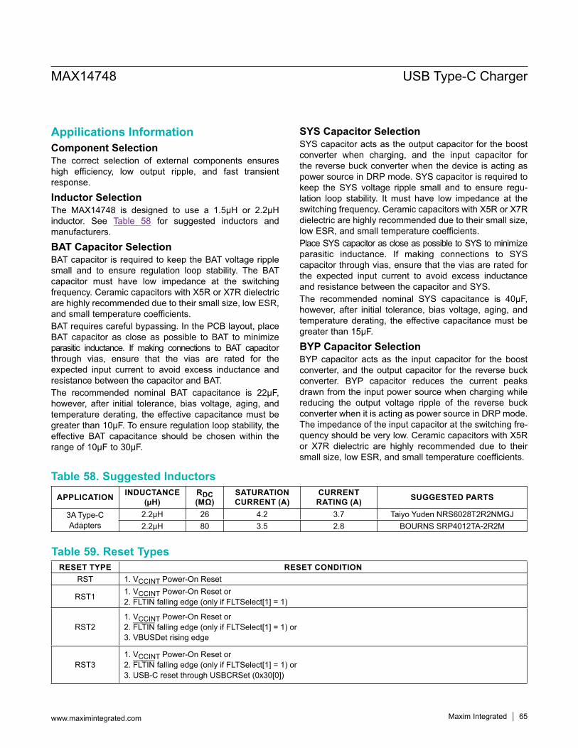
Appilications InformationComponent SelectionThe correct selection of external components ensures high efficiency, low output ripple, and fast transient response.
Inductor SelectionThe MAX14748 is designed to use a 1.5μH or 2.2μH inductor. See Table 58 for suggested inductors and manufacturers.
BAT Capacitor Selection BAT capacitor is required to keep the BAT voltage ripple small and to ensure regulation loop stability. The BAT capacitor must have low impedance at the switching frequency. Ceramic capacitors with X5R or X7R dielectric are highly recommended due to their small size, low ESR, and small temperature coefficients. BAT requires careful bypassing. In the PCB layout, place BAT capacitor as close as possible to BAT to minimize parasitic inductance. If making connections to BAT capacitor through vias, ensure that the vias are rated for the expected input current to avoid excess inductance and resistance between the capacitor and BAT. The recommended nominal BAT capacitance is 22μF, however, after initial tolerance, bias voltage, aging, and temperature derating, the effective capacitance must be greater than 10μF. To ensure regulation loop stability, the effective BAT capacitance should be chosen within the range of 10μF to 30μF.
SYS Capacitor SelectionSYS capacitor acts as the output capacitor for the boost converter when charging, and the input capacitor for the reverse buck converter when the device is acting as power source in DRP mode. SYS capacitor is required to keep the SYS voltage ripple small and to ensure regu-lation loop stability. It must have low impedance at the switching frequency. Ceramic capacitors with X5R or X7R dielectric are highly recommended due to their small size, low ESR, and small temperature coefficients. Place SYS capacitor as close as possible to SYS to minimize parasitic inductance. If making connections to SYS capacitor through vias, ensure that the vias are rated for the expected input current to avoid excess inductance and resistance between the capacitor and SYS. The recommended nominal SYS capacitance is 40μF, however, after initial tolerance, bias voltage, aging, and temperature derating, the effective capacitance must be greater than 15μF.
BYP Capacitor Selection BYP capacitor acts as the input capacitor for the boost converter, and the output capacitor for the reverse buck converter. BYP capacitor reduces the current peaks drawn from the input power source when charging while reducing the output voltage ripple of the reverse buck converter when it is acting as power source in DRP mode. The impedance of the input capacitor at the switching fre-quency should be very low. Ceramic capacitors with X5R or X7R dielectric are highly recommended due to their small size, low ESR, and small temperature coefficients.
Table 59. Reset Types
Table 58. Suggested Inductors
RESET TYPE RESET CONDITIONRST 1. VCCINT Power-On Reset
RST1 1. VCCINT Power-On Reset or 2. FLTIN falling edge (only if FLTSelect[1] = 1)
RST21. VCCINT Power-On Reset or2. FLTIN falling edge (only if FLTSelect[1] = 1) or3. VBUSDet rising edge
RST31. VCCINT Power-On Reset or2. FLTIN falling edge (only if FLTSelect[1] = 1) or3. USB-C reset through USBCRSet (0x30[0])
APPLICATION INDUCTANCE (µH)
RDC (MΩ)
SATURATION CURRENT (A)
CURRENT RATING (A) SUGGESTED PARTS
3A Type-C Adapters
2.2μH 26 4.2 3.7 Taiyo Yuden NRS6028T2R2NMGJ2.2μH 80 3.5 2.8 BOURNS SRP4012TA-2R2M
MAX14748 USB Type-C Charger
www.maximintegrated.com Maxim Integrated │ 65
BYP requires careful bypassing. In the PCB layout, place BYP capacitor as close as possible to the BYP to mini-mize parasitic inductance. If making connections to BYP capacitor through vias, ensure that the vias are rated for the expected input current to avoid excess inductance and resistance between the capacitor and BYP.The recommended nominal BYP capacitance is 22μF, however, after initial tolerance, bias voltage, aging, and temperature derating, the effective capacitance must be greater than 10μF.
CHGIN Capacitor SelectionCHGIN capacitor decouples a charge source and its parasitic impedance. Typically, the charger source at CHGIN is a USB connector’s VBUS. The recommended nominal CHGIN capacitance is 1μF. Larger capacitance at CHGIN improves the decoupling; however, take care not to exceed the maximum capacitance allowed by the USB specification.The impedance of the CHGIN at the DC-DC switching fre-quency should be very low. Ceramic capacitors with X5R or X7R dielectric are highly recommended due to their small size, low ESR, and small temperature coefficients.
To fully utilize the +30V input capability of the, choose a capacitor with a 35V or greater rating; many applications don’t need to utilize the full input capability of the device and find that a 16V or 10V rated input capacitor is suf-ficient.
BST Capacitor SelectionChoose the nominal BST capacitance to be 0.1μF. BST capacitor is part of a charge pump that creates the high-side gate drive for the DC-DC. It is recommended that the BST capacitor has at least 10V rating.
PCB Layout and RoutingHigh switching frequencies and large peak currents make PCB layout a very important part of design. Good design minimizes excessive EMI on the feedback paths and voltage gradients in the ground plane, both of which can result in instability or regulation errors. Connect the inductor, input capacitors, and output capacitors as close together as possible, and keep their traces short, direct, and wide. Keep noisy traces, such as the LX node, as short as possible.
MAX14748 USB Type-C Charger
www.maximintegrated.com Maxim Integrated │ 66
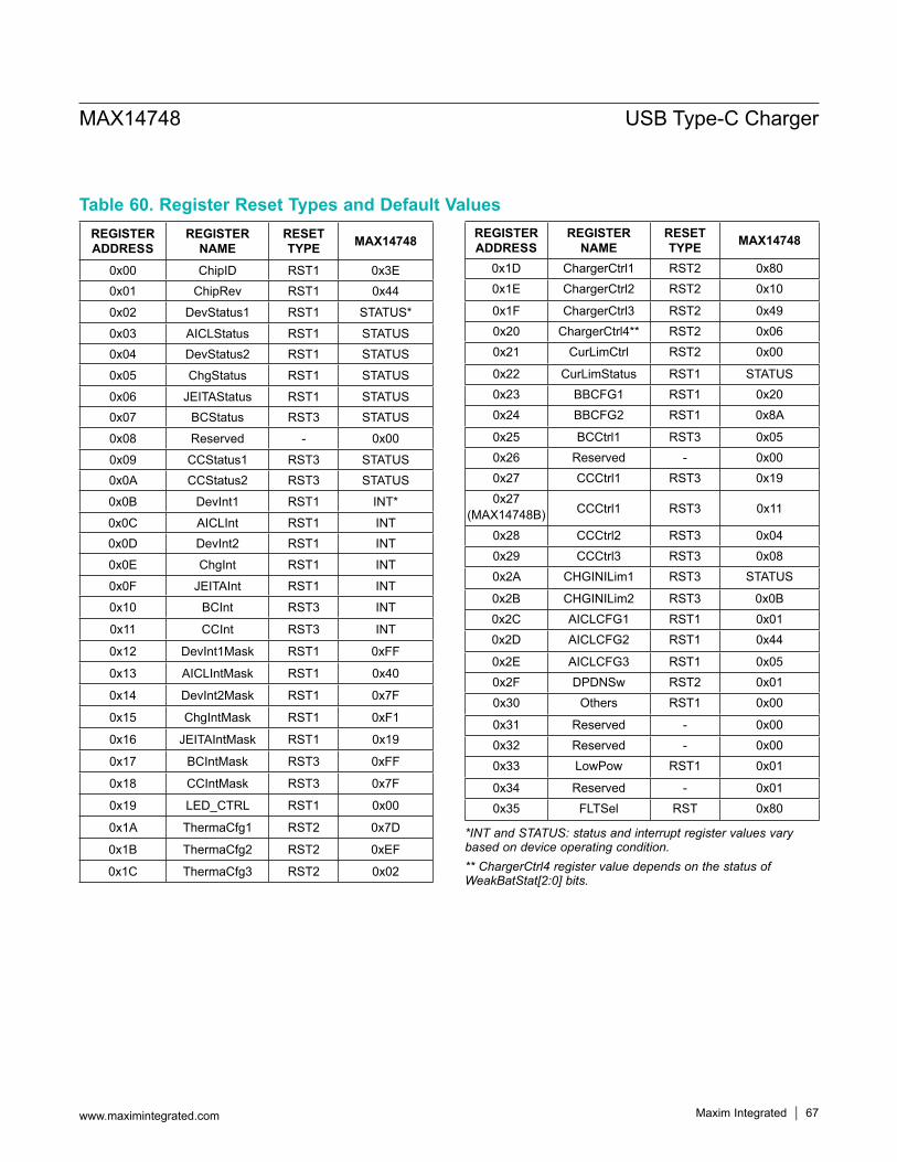
Table 60. Register Reset Types and Default Values
*INT and STATUS: status and interrupt register values vary based on device operating condition.** ChargerCtrl4 register value depends on the status of WeakBatStat[2:0] bits.
REGISTER ADDRESS
REGISTER NAME
RESET TYPE MAX14748
0x00 ChipID RST1 0x3E0x01 ChipRev RST1 0x440x02 DevStatus1 RST1 STATUS*0x03 AICLStatus RST1 STATUS0x04 DevStatus2 RST1 STATUS0x05 ChgStatus RST1 STATUS0x06 JEITAStatus RST1 STATUS0x07 BCStatus RST3 STATUS0x08 Reserved - 0x000x09 CCStatus1 RST3 STATUS0x0A CCStatus2 RST3 STATUS0x0B DevInt1 RST1 INT*0x0C AICLInt RST1 INT0x0D DevInt2 RST1 INT0x0E ChgInt RST1 INT0x0F JEITAInt RST1 INT0x10 BCInt RST3 INT
0x11 CCInt RST3 INT
0x12 DevInt1Mask RST1 0xFF
0x13 AICLIntMask RST1 0x40
0x14 DevInt2Mask RST1 0x7F
0x15 ChgIntMask RST1 0xF1
0x16 JEITAIntMask RST1 0x19
0x17 BCIntMask RST3 0xFF
0x18 CCIntMask RST3 0x7F
0x19 LED_CTRL RST1 0x00
0x1A ThermaCfg1 RST2 0x7D
0x1B ThermaCfg2 RST2 0xEF
0x1C ThermaCfg3 RST2 0x02
REGISTER ADDRESS
REGISTER NAME
RESET TYPE MAX14748
0x1D ChargerCtrl1 RST2 0x800x1E ChargerCtrl2 RST2 0x10
0x1F ChargerCtrl3 RST2 0x490x20 ChargerCtrl4** RST2 0x060x21 CurLimCtrl RST2 0x00
0x22 CurLimStatus RST1 STATUS0x23 BBCFG1 RST1 0x200x24 BBCFG2 RST1 0x8A
0x25 BCCtrl1 RST3 0x050x26 Reserved - 0x000x27 CCCtrl1 RST3 0x190x27
(MAX14748B) CCCtrl1 RST3 0x11
0x28 CCCtrl2 RST3 0x040x29 CCCtrl3 RST3 0x080x2A CHGINILim1 RST3 STATUS
0x2B CHGINILim2 RST3 0x0B0x2C AICLCFG1 RST1 0x010x2D AICLCFG2 RST1 0x44
0x2E AICLCFG3 RST1 0x050x2F DPDNSw RST2 0x010x30 Others RST1 0x00
0x31 Reserved - 0x000x32 Reserved - 0x000x33 LowPow RST1 0x01
0x34 Reserved - 0x010x35 FLTSel RST 0x80
MAX14748 USB Type-C Charger
www.maximintegrated.com Maxim Integrated │ 67
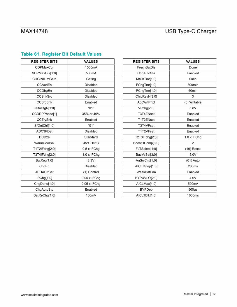
Table 61. Register Bit Default ValuesREGISTER BITS VALUES
CDPMaxCur 1500mA
SDPMaxCur[1:0] 500mA
CHGINILimGate Gating
CCAudEn Disabled
CCDbgEn Disabled
CCSnkSrc Disabled
CCSrcSnk Enabled
JeitaCfgR[1:0] “01”
CCDRPPhase[1] 35% or 40%
CCTrySnk Enabled
SfOutCtrl[1:0] “01”
ADC3PDet Disabled
DCD2s Standard
WarmCoolSel 45°C/10°C
T1T2IFchg[2:0] 0.5 x IFChg
T3T4IFchg[2:0] 1.0 x IFChg
BatReg[1:0] 8.3V
ChgEn Disabled
JETIACtrSet (1) Control
IPChg[1:0] 0.05 x IFChg
ChgDone[1:0] 0.05 x IFChg
ChgAutoStp Enabled
BatReChg[1:0] 100mV
REGISTER BITS VALUESFreshBatDis Done
ChgAutoSta Enabled
MtChTmr[1:0] 0min
FChgTmr[1:0] 300min
PChgTmr[1:0] 60min
ChipRevH[3:0] 3
AppWrtPrtct (0) Writable
VPchg[2:0] 5.8V
T3T4ENset Enabled
T1T2ENset Enabled
T3T4VFset Enabled
T1T2VFset Enabled
T2T3IFchg[2:0] 1.0 x IFChg
BoostRComp[3:0] 2
FLTSelect[1:0] (10) Reset
BuckVSet[3:0] 5.0V
AnSwCntl[1:0] (01) Auto
AICLTStep[1:0] 200ms
WeakBatEna Enabled
BYPUVLO{2:0] 4.0V
AICLMax[4:0] 500mA
BYPDeb 500µs
AICLTBlk[1:0] 1000ms
MAX14748 USB Type-C Charger
www.maximintegrated.com Maxim Integrated │ 68
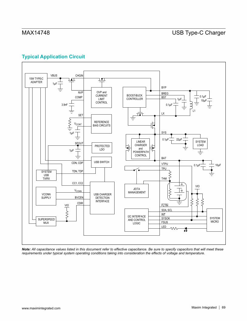
Note: All capacitance values listed in this document refer to effective capacitance. Be sure to specify capacitors that will meet these requirements under typical system operating conditions taking into consideration the effects of voltage and temperature.
15W TYPE-CADAPTER
OVP andCURRENT
LIMITCONTROL
REFERENCEBIAS CIRCUITS
LINEARCHARGER
andPOWERPATH
CONTROL
PROTECTEDLDO
SYSTEMUSB
TX/RX
VCONNSUPPLY
USB CHARGERDETECTIONINTERFACE
USB SWITCH
BOOST-BUCKCONTROLLER
SYSTEMLOAD
I2C INTERFACEAND CONTROL
LOGIC
JEITAMANAGEMENT
SYSTEMMICRO
SUPERSPEEDMUX
CHGIN
NVP
SET
VCCINT
SFOUT
CDN, CDP
TDN, TDP
CC1, CC2
VCONN
BVCEN
CDIRVIO
VIO
THM
TPU
VTPU
BAT
FLTINSDA, SCL
INTSYSOKFSUS
LED
BYP
BREGBST
LX
SYS
1µF
0.1µF10µF
L1
1µF
0.1µF
22µF
10µF
1µF
1µF
VBUS
COMP
3.9nF
0.1µF
0.1µF
MAX14748 USB Type-C Charger
www.maximintegrated.com Maxim Integrated │ 69
Typical Application Circuit
+Denotes a lead(Pb)-free package/RoHS-compliant package.See Table 61 for the device differences.T = Tape and reel.*Denotes a future product.
PART TEMP RANGE PIN-PACKAGEMAX14748EWW+ -40ºC to +85ºC 54 WLPMAX14748EWW+T -40ºC to +85ºC 54 WLP
MAX14748BEWW+* -40ºC to +85ºC 54 WLP
MAX14748BEWW+T* -40ºC to +85ºC 54 WLP
PACKAGE TYPE
PACKAGE CODE
OUTLINE NO.
LAND PATTERN NO.
54 WLP W542C3+1 21-100122Refer to
Application Note 1891
MAX14748 USB Type-C Charger
www.maximintegrated.com Maxim Integrated │ 70
Ordering Information Chip InformationPROCESS: BiCMOS
Package InformationFor the latest package outline information and land patterns (footprints), go to www.maximintegrated.com/packages. Note that a “+”, “#”, or “-” in the package code indicates RoHS status only. Package drawings may show a different suffix character, but the drawing pertains to the package regardless of RoHS status.
REVISIONNUMBER
REVISIONDATE DESCRIPTION PAGES
CHANGED
0 6/17 Initial release —
1 12/17 Added MAX14748C as furure product 1, 6, 27, 29, 35, 36, 52, 58, 59, 67, 68, 70
2 3/18 Updated Bump Configuration, Figure 4, Register Map, Table 33, Table 60, and Ordering Information table 15, 27, 35, 52,
3 4/18 Updated Electrical Characteristics table, Register Map, Tables 8, 17, 24, 33 3, 35, 38, 43, 47, 52
3.1 5/18 Corrected Bump Configuration typo 15
Maxim Integrated cannot assume responsibility for use of any circuitry other than circuitry entirely embodied in a Maxim Integrated product. No circuit patent licenses are implied. Maxim Integrated reserves the right to change the circuitry and specifications without notice at any time. The parametric values (min and max limits) shown in the Electrical Characteristics table are guaranteed. Other parametric values quoted in this data sheet are provided for guidance.
Maxim Integrated and the Maxim Integrated logo are trademarks of Maxim Integrated Products, Inc.
MAX14748 USB Type-C Charger
© 2018 Maxim Integrated Products, Inc. │ 71
Revision History
For pricing, delivery, and ordering information, please contact Maxim Direct at 1-888-629-4642, or visit Maxim Integrated’s website at www.maximintegrated.com.