Embed Size (px)
Citation preview
Cleanroom Considerations for
ESD ControlChristopher W. Long
IBM
2007 SEMI NA ESD Workshop

Agenda
Cleanroom/Environment Static Charge Challenges
Control Strategies
Case Studies
Summary and Acknowledgements

Static Charge Problems:Contamination and ESD
Yield Throughput
Reticles
Equipment
Contamination Process Interruptions
WafersIntegratedCircuits
ESD Damage
Static ChargeStatic Charge +
+
+++
+
------
---
-----
------
Equipment SurfacesPellicles
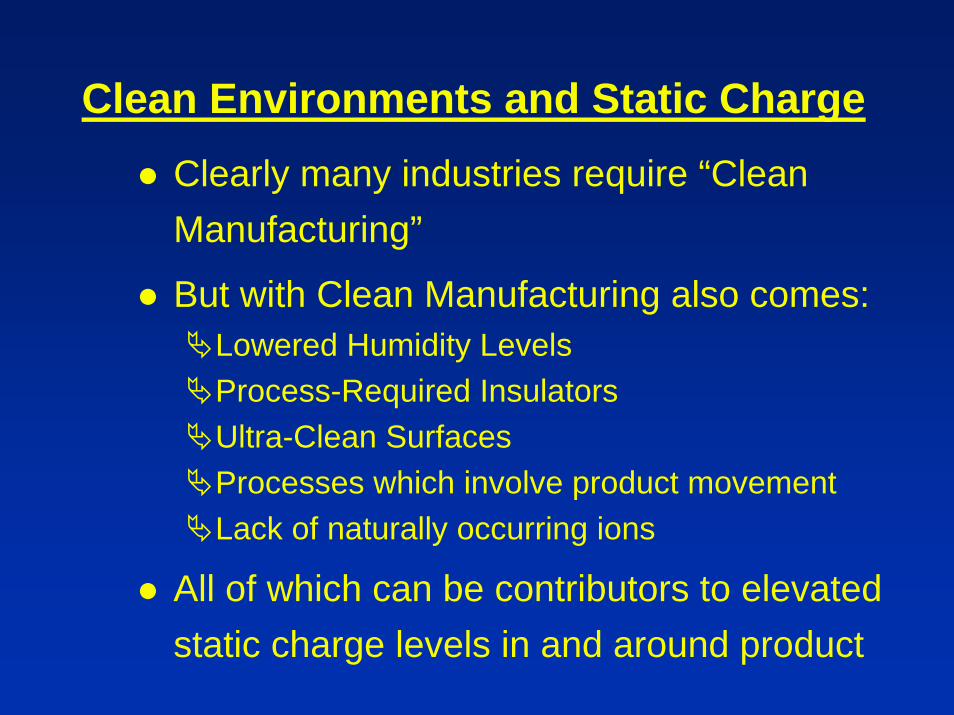
Clean Environments and Static Charge Clearly many industries require “Clean Manufacturing”
But with Clean Manufacturing also comes:Lowered Humidity LevelsProcess-Required InsulatorsUltra-Clean SurfacesProcesses which involve product movementLack of naturally occurring ions
All of which can be contributors to elevated static charge levels in and around product
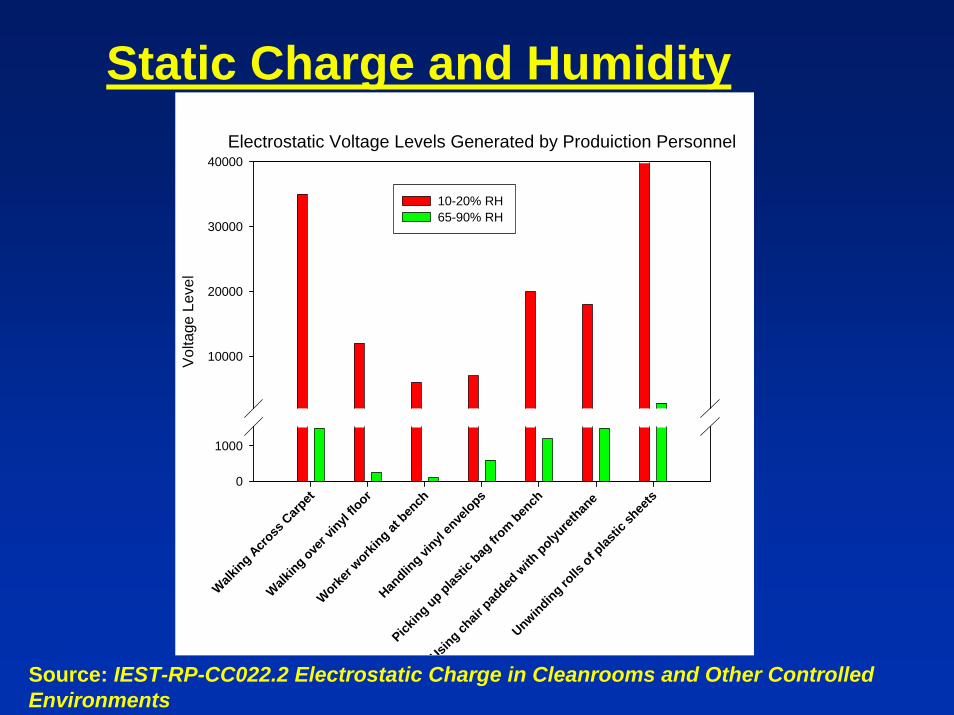
Static Charge and HumidityElectrostatic Voltage Levels Generated by Produiction Personnel
Walking Acro
ss C
arpet
Walking ove
r vinyl
floor
Worker w
orking at
bench
Handlin
g vinyl
enve
lops
Picking up plas
tic bag
from ben
ch
Using ch
air pad
ded w
ith polyu
rethan
e
Unwinding rolls
of plas
tic sh
eets
Volta
ge L
evel
0
1000
10000
20000
30000
40000
10-20% RH 65-90% RH
Source: IEST-RP-CC022.2 Electrostatic Charge in Cleanrooms and Other Controlled Environments

Humidity
Cleanroom humidity level specs intentionally kept at low levels
Typically between 30 and 45% RH
Driven by tooling, product requirements
Humidity can affect levels of generated static charge
However provides ineffective method of static control once it exists
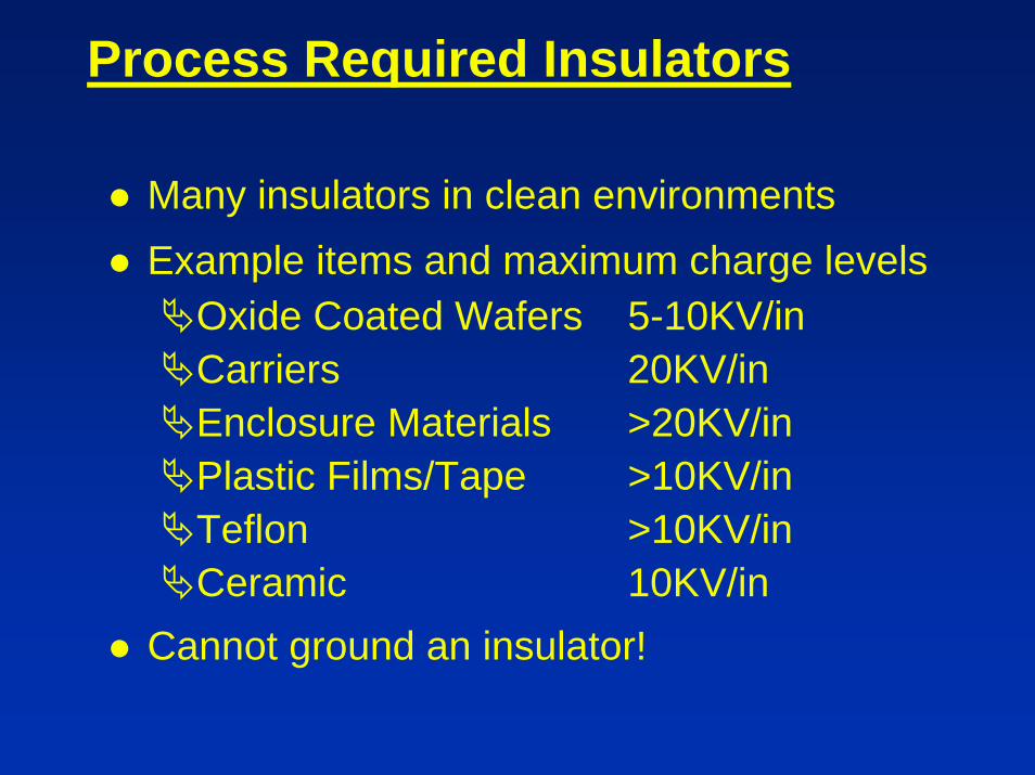
Process Required Insulators
Many insulators in clean environmentsExample items and maximum charge levels
Oxide Coated Wafers 5-10KV/inCarriers 20KV/inEnclosure Materials >20KV/inPlastic Films/Tape >10KV/inTeflon >10KV/inCeramic 10KV/in
Cannot ground an insulator!

Ultra-Clean Surfaces
Cleanroom protocol typically calls for frequent cleaning of surfaces, Result:
Minimize conductive film of contamination that helps dissipative chargeAct of cleaning/wiping surfaces can itself can result in tribo-charging of insulators
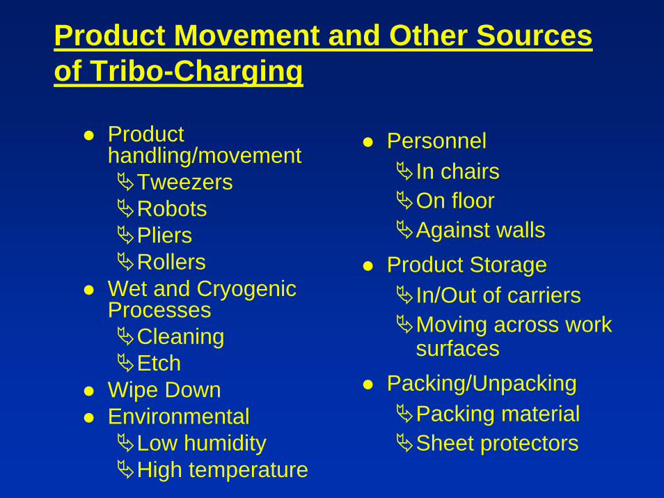
Product Movement and Other Sources of Tribo-Charging
Product handling/movement
TweezersRobotsPliersRollers
Wet and Cryogenic Processes
CleaningEtch
Wipe DownEnvironmental
Low humidityHigh temperature
PersonnelIn chairsOn floorAgainst walls
Product StorageIn/Out of carriersMoving across work surfaces
Packing/UnpackingPacking materialSheet protectors
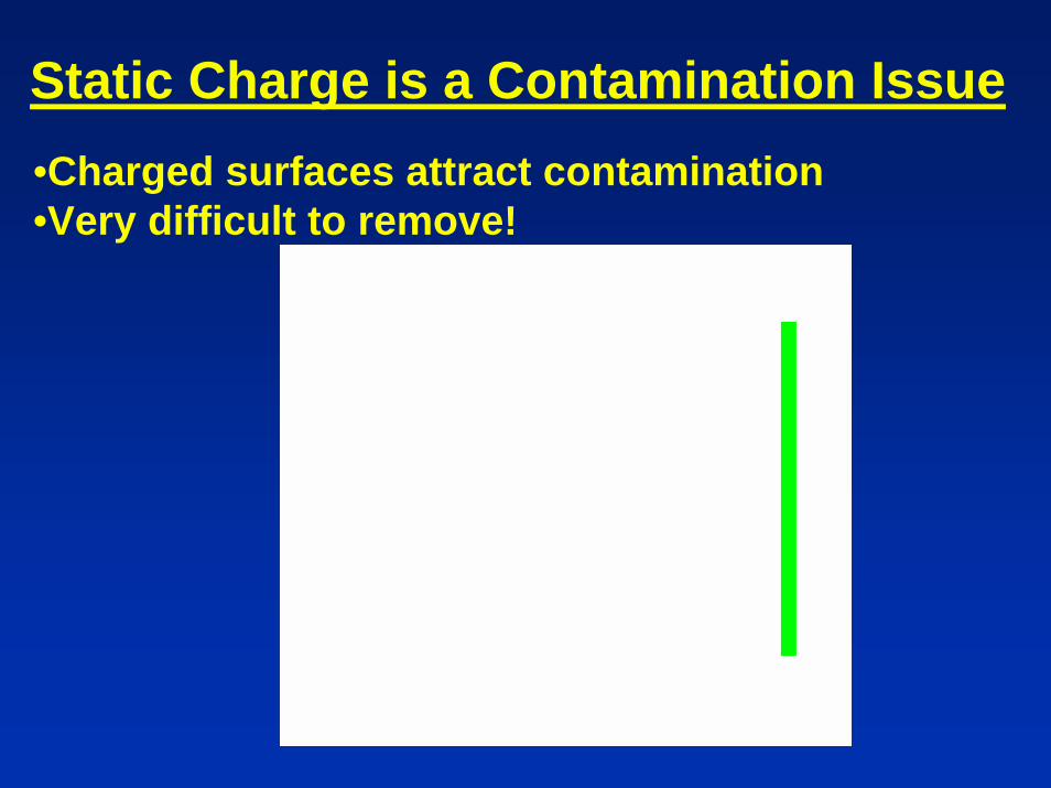
Static Charge is a Contamination Issue•Charged surfaces attract contamination •Very difficult to remove!
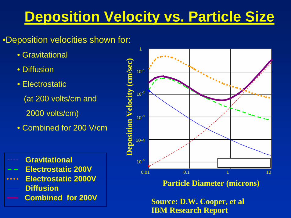
Deposition Velocity vs. Particle Size
Particle Diameter (microns)0.01 0.1 1 10
Dep
ositi
on V
eloc
ity (c
m/s
ec)
-5
-3
-2
-1
10
10-4
10
10
10
1
Source: D.W. Cooper, et al IBM Research Report
GravitationalElectrostatic 200VElectrostatic 2000VDiffusionCombined for 200V
•Deposition velocities shown for:• Gravitational
• Diffusion
• Electrostatic
(at 200 volts/cm and
2000 volts/cm)
• Combined for 200 V/cm
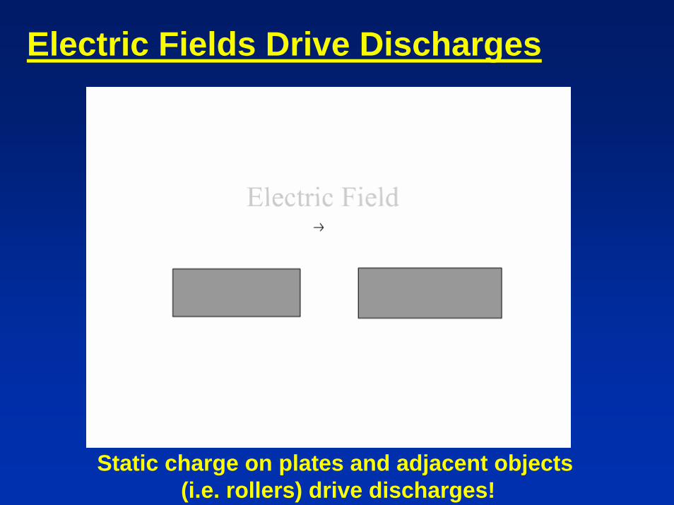
Electric Fields Drive Discharges
Static charge on plates and adjacent objects(i.e. rollers) drive discharges!
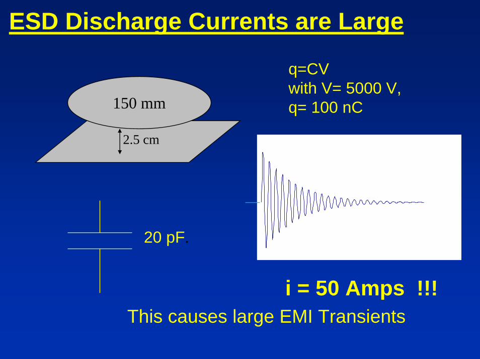
ESD Discharge Currents are Large
2.5 cm
20 pF.
q=CVwith V= 5000 V,q= 100 nC150 mm
i = 50 Amps !!!This causes large EMI Transients
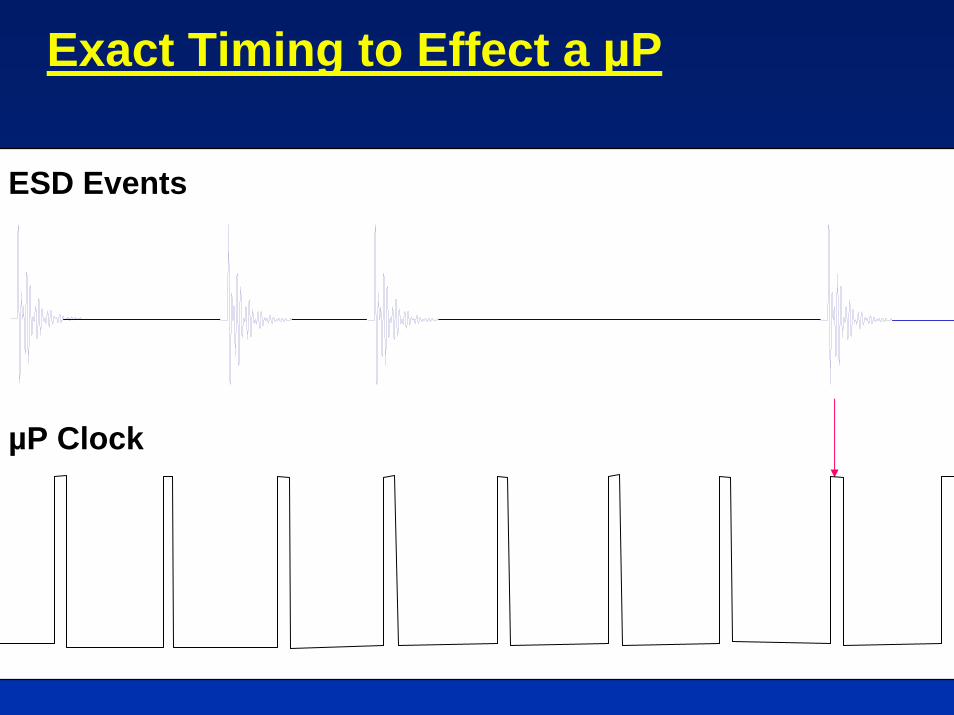
Exact Timing to Effect a µP
ESD Events
µP Clock
Agenda
Cleanroom/Environment Static Charge Challenges
Control Strategies
Case Studies
Summary and Acknowledgements
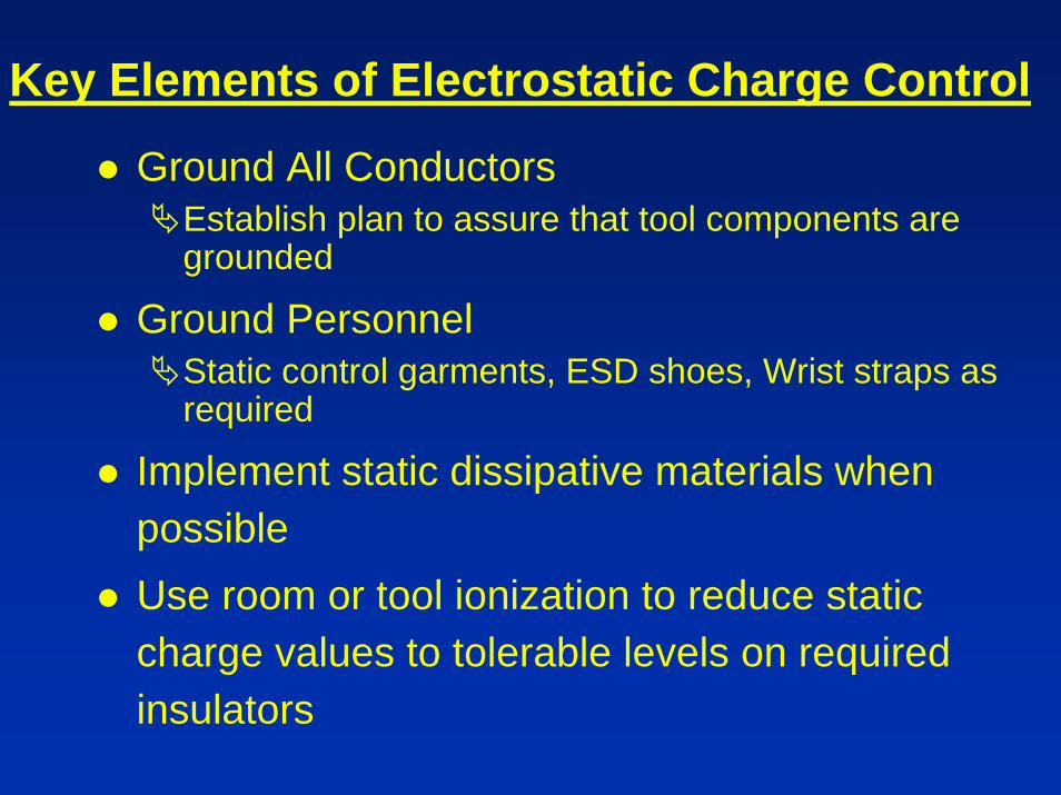
Key Elements of Electrostatic Charge Control
Ground All ConductorsEstablish plan to assure that tool components are grounded
Ground PersonnelStatic control garments, ESD shoes, Wrist straps as required
Implement static dissipative materials when possibleUse room or tool ionization to reduce static charge values to tolerable levels on required insulators
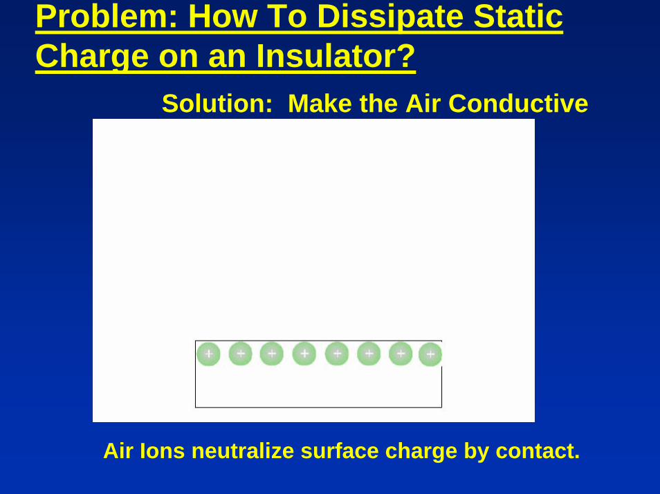
Problem: How To Dissipate Static Charge on an Insulator?
Solution: Make the Air Conductive
Air Ions neutralize surface charge by contact.
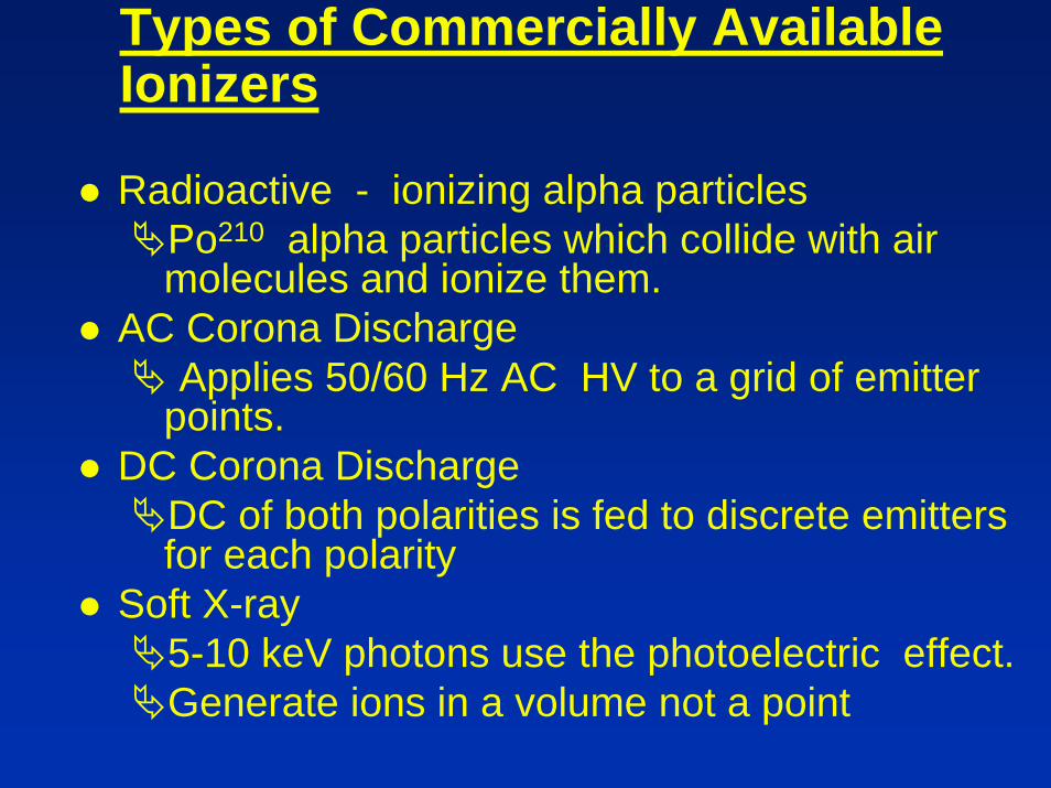
Types of Commercially Available Ionizers
Radioactive - ionizing alpha particlesPo210 alpha particles which collide with air molecules and ionize them.
AC Corona Discharge Applies 50/60 Hz AC HV to a grid of emitter
points.DC Corona Discharge
DC of both polarities is fed to discrete emitters for each polarity
Soft X-ray 5-10 keV photons use the photoelectric effect.Generate ions in a volume not a point
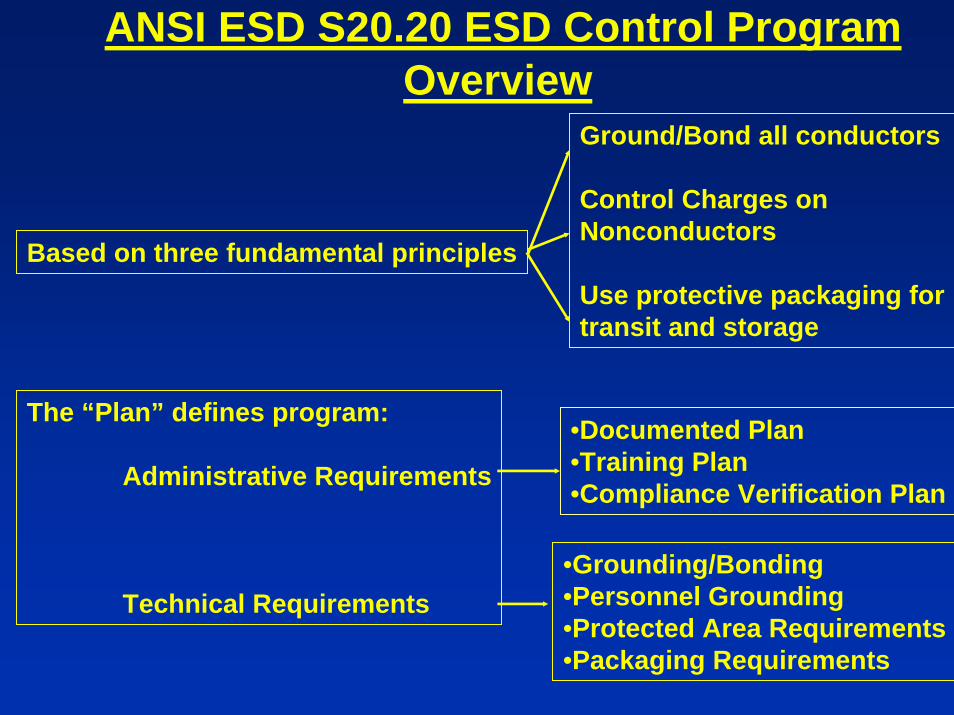
ANSI ESD S20.20 ESD Control Program Overview
Based on three fundamental principles
The “Plan” defines program:
Administrative Requirements
Technical Requirements
Ground/Bond all conductors
Control Charges on Nonconductors
Use protective packaging fortransit and storage
•Documented Plan•Training Plan•Compliance Verification Plan
•Grounding/Bonding•Personnel Grounding•Protected Area Requirements•Packaging Requirements
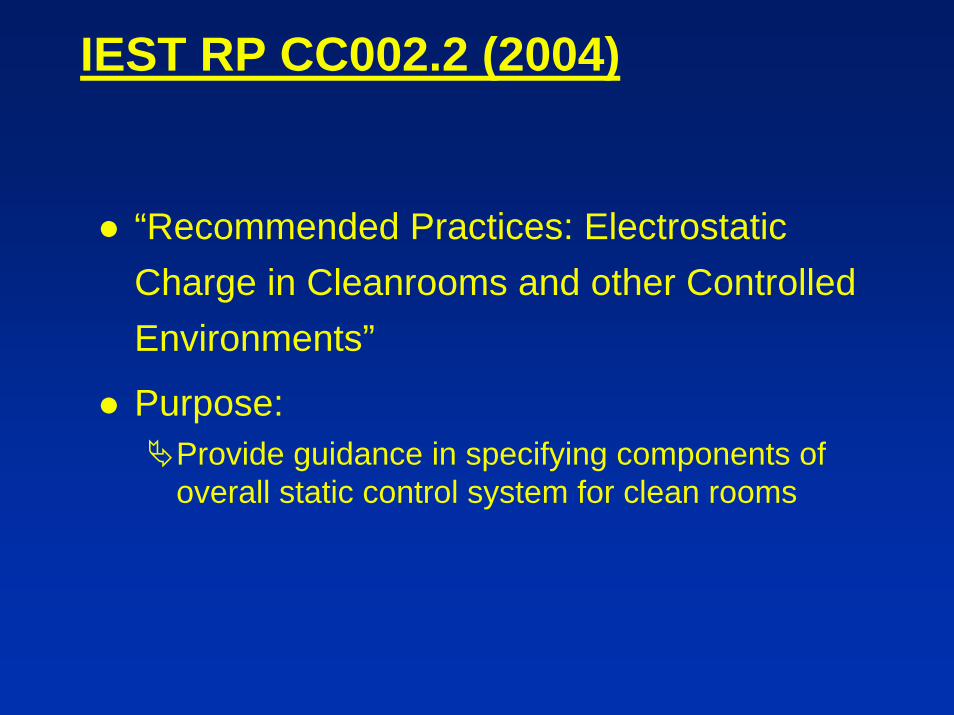
IEST RP CC002.2 (2004)
“Recommended Practices: Electrostatic Charge in Cleanrooms and other Controlled Environments”
Purpose: Provide guidance in specifying components of overall static control system for clean rooms

IEST RP CC002.2 Basic Methods
Electrostatic Charge Control (ESCC)/Electrostatic Discharge Control (ESDC) Basic Methods
Ground all tool/facilities componentsReasonable and appropriate use of conductive/static dissipative materials
Includes personnel garmentingUse of local and/or room ionization to control charge on insulatorsImplementation of personnel training in area of ESD control
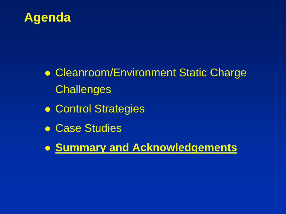
Agenda
Cleanroom/Environment Static Charge Challenges
Control Strategies
Case Studies
Summary and Acknowledgements
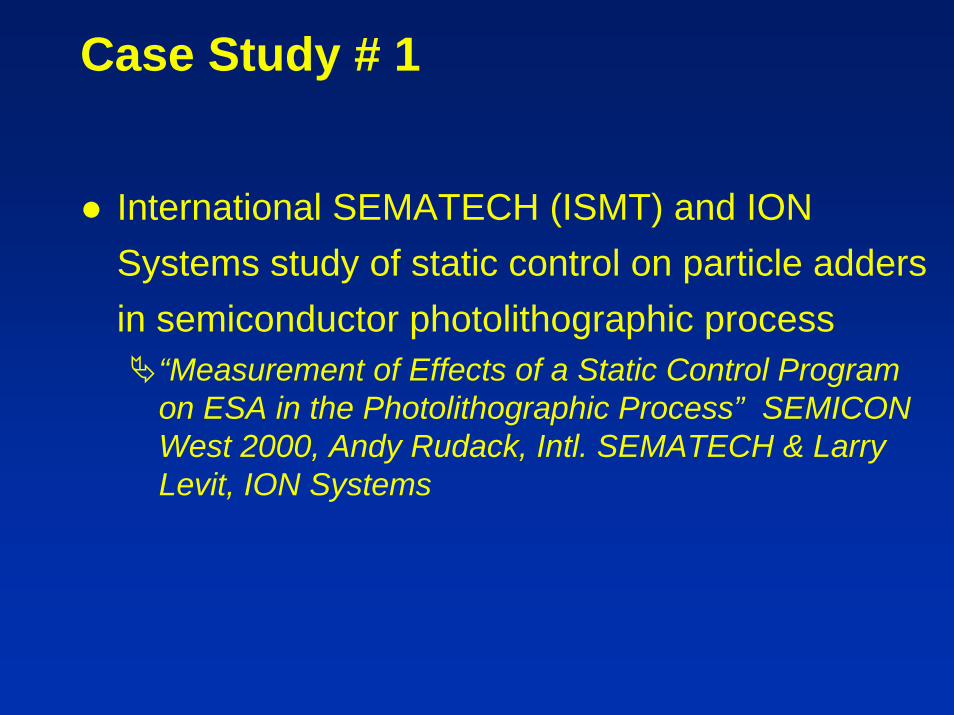
Case Study # 1
International SEMATECH (ISMT) and ION Systems study of static control on particle adders in semiconductor photolithographic process
“Measurement of Effects of a Static Control Program on ESA in the Photolithographic Process” SEMICON West 2000, Andy Rudack, Intl. SEMATECH & Larry Levit, ION Systems
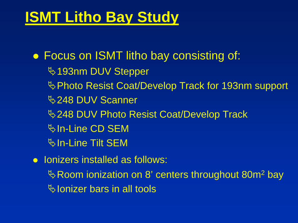
ISMT Litho Bay Study
Focus on ISMT litho bay consisting of:193nm DUV StepperPhoto Resist Coat/Develop Track for 193nm support248 DUV Scanner248 DUV Photo Resist Coat/Develop Track In-Line CD SEMIn-Line Tilt SEM
Ionizers installed as follows:Room ionization on 8’ centers throughout 80m2 bayIonizer bars in all tools

ISMT Litho Bay Study Experiment
25 test monitor wafers pre-scanned for defects6000A oxide insulator coating on each waferPre-Scanned on KLA-Tencor 6420 SurfScan
Wafers cycled 23.5 hours in 193nm Track Ionization turned on and allowed to equilibrate1050 number of wafer passesRescanned on KLA-Tencor 6420
Wafers cycled 10.5 hours in 193nm TrackIonization turned off and allowed to equilibrate562 wafer passesRescanned on KLA-Tencor 6420

Ionizer Installation
In the Room As well as in Tool
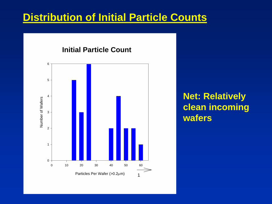
Initial Particle Count
Particles Per Wafer (>0.2μm)
0 10 20 30 40 50 60
Num
ber o
f Waf
ers
0
1
2
3
4
5
6
1
Distribution of Initial Particle Counts
Net: Relatively clean incoming wafers

Distribution of PWP Values
PWP Histogram with Ionization Off
PWP
-0.1 0.0 0.1 0.2 0.3 0.4 0.5 0.6 0.7 0.8 0.9 1.0
Freq
uenc
y of
Occ
uren
ce
0
1
2
3
4
5
6PWP Histogram With Ionization On
PWP
-0.1 0.0 0.1 0.2 0.3 0.4 0.5 0.6 0.7 0.8 0.9 1.0
Freq
uenc
y of
Occ
uren
ce
0
1
2
3
4
5
6
7
•PWP: Particles per Wafer Pass
•PWP=(particlesbefore-particlesafter/number of passes)
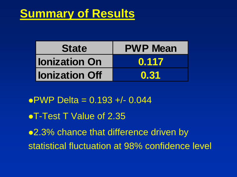
Summary of Results
State PWP MeanIonization On 0.117Ionization Off 0.31
PWP Delta = 0.193 +/- 0.044
T-Test T Value of 2.35
2.3% chance that difference driven by statistical fluctuation at 98% confidence level
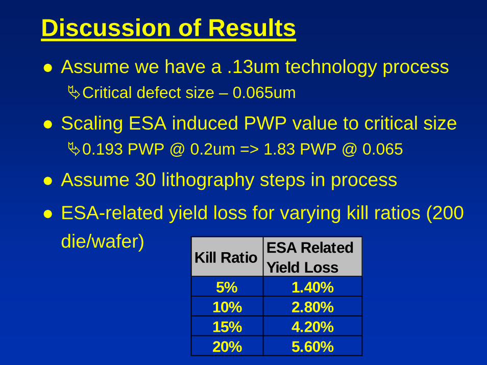
Discussion of ResultsAssume we have a .13um technology process
Critical defect size – 0.065um
Scaling ESA induced PWP value to critical size0.193 PWP @ 0.2um => 1.83 PWP @ 0.065
Assume 30 lithography steps in process
ESA-related yield loss for varying kill ratios (200 die/wafer)
Kill Ratio ESA Related Yield Loss
5% 1.40%10% 2.80%15% 4.20%20% 5.60%
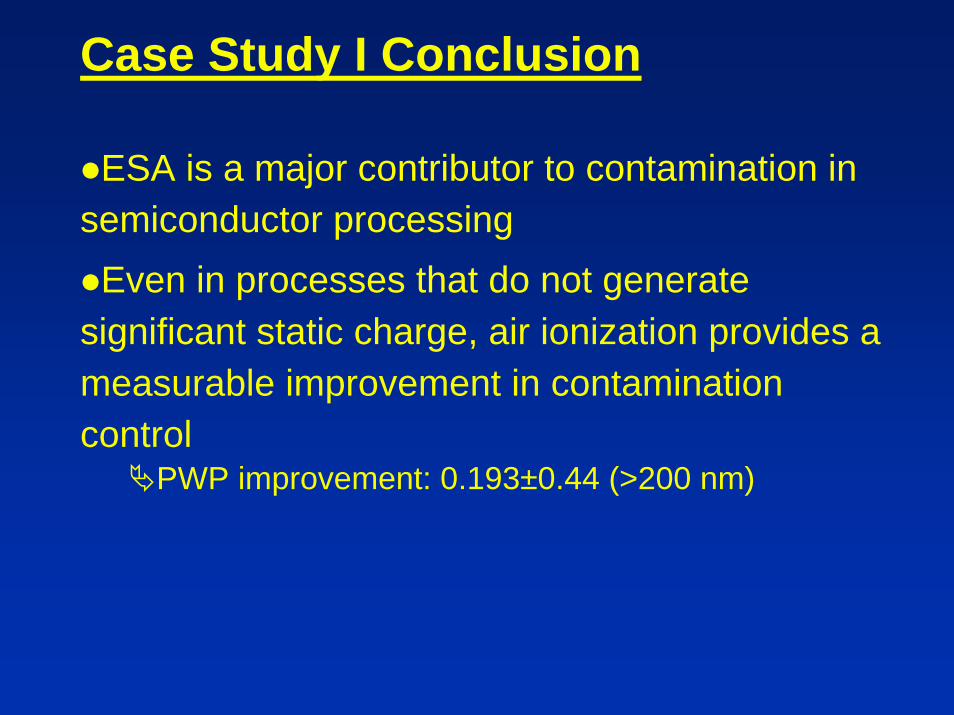
Case Study I Conclusion
ESA is a major contributor to contamination in semiconductor processing
Even in processes that do not generate significant static charge, air ionization provides a measurable improvement in contamination control
PWP improvement: 0.193±0.44 (>200 nm)
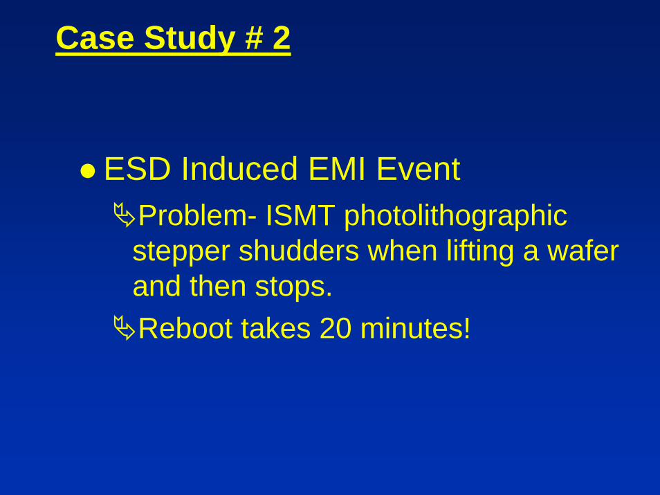
Case Study # 2
ESD Induced EMI Event Problem- ISMT photolithographic stepper shudders when lifting a wafer and then stops. Reboot takes 20 minutes!

Stepper Process Schematic
To Track Wafer Aligner
Exposure stage
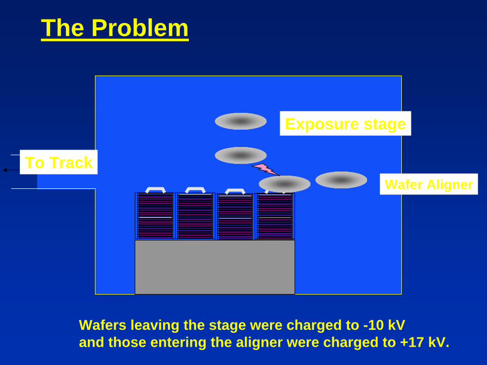
The Problem
To TrackWafer Aligner
Exposure stage
Wafers leaving the stage were charged to -10 kV and those entering the aligner were charged to +17 kV.
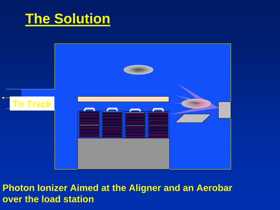
The Solution
To Track
Photon Ionizer Aimed at the Aligner and an Aerobarover the load station
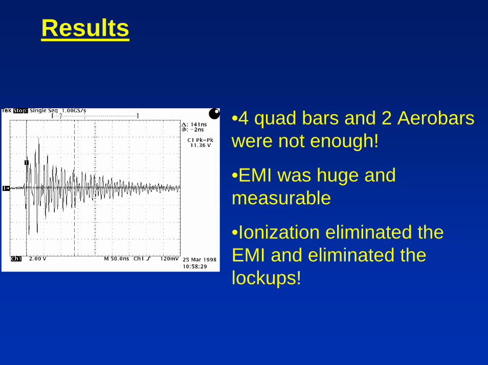
Results
•4 quad bars and 2 Aerobarswere not enough!
•EMI was huge and measurable
•Ionization eliminated the EMI and eliminated the lockups!

Case Study # 3
ESD Impact On In-Process Wafer DieProblem: Oxide Cracking Damage on Center Wafer Die in Spin Dry Process
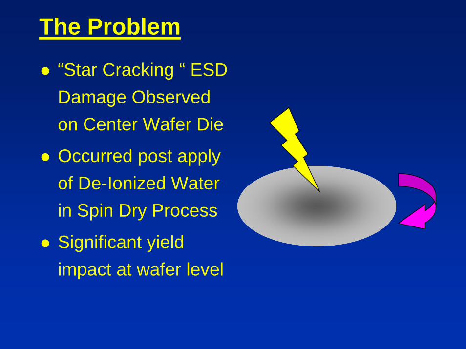
The Problem
“Star Cracking “ ESD Damage Observed on Center Wafer Die
Occurred post apply of De-Ionized Water in Spin Dry Process
Significant yield impact at wafer level
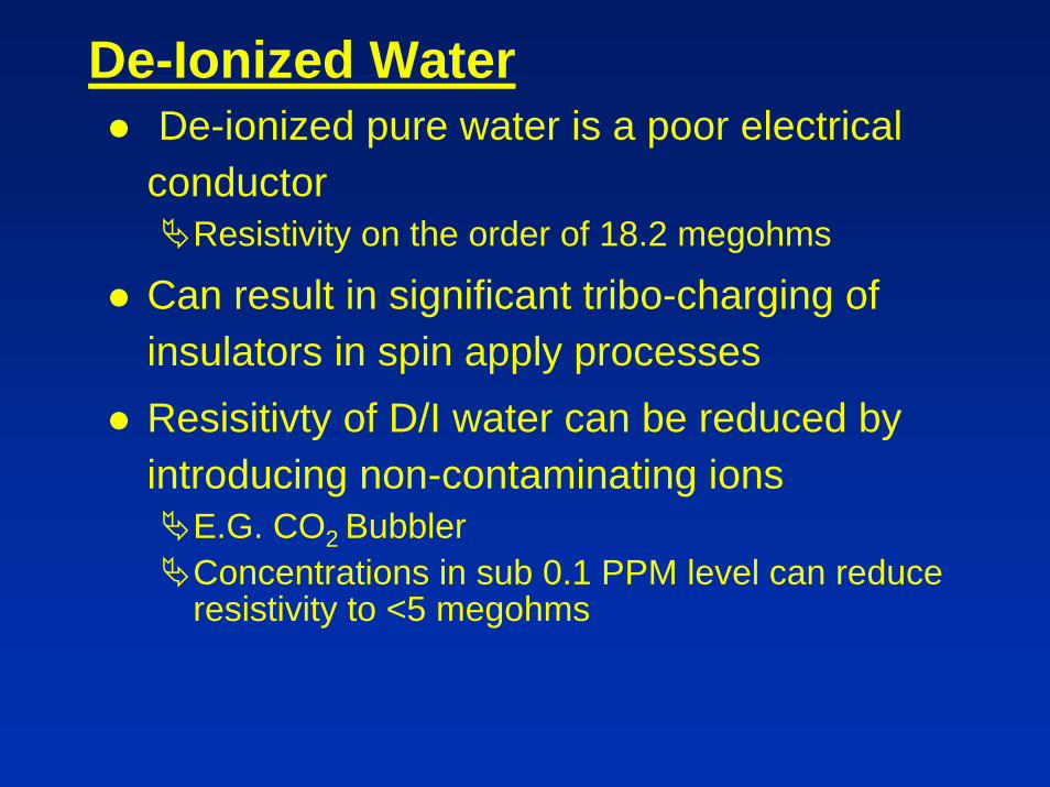
De-Ionized WaterDe-ionized pure water is a poor electrical
conductorResistivity on the order of 18.2 megohms
Can result in significant tribo-charging of insulators in spin apply processesResisitivty of D/I water can be reduced by introducing non-contaminating ions
E.G. CO2 BubblerConcentrations in sub 0.1 PPM level can reduce resistivity to <5 megohms
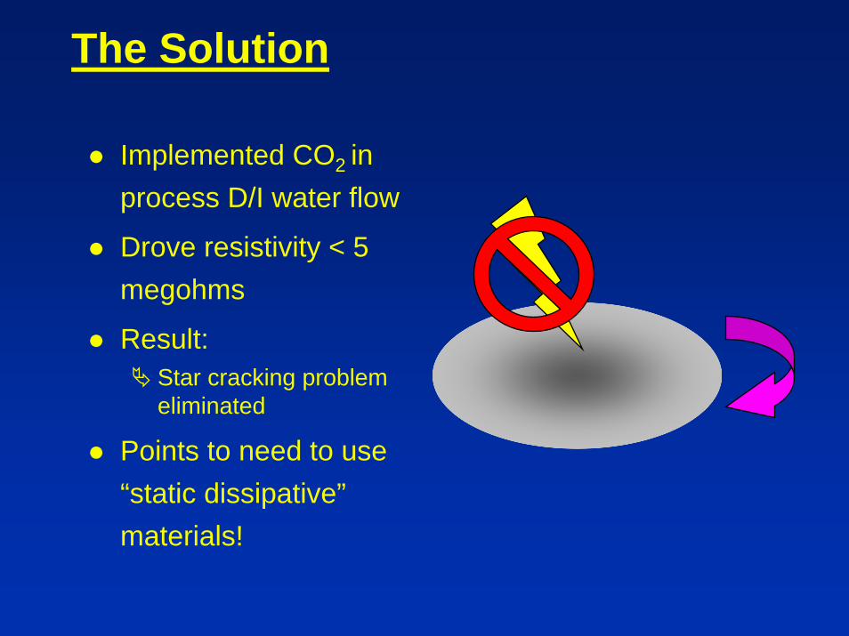
The Solution
Implemented CO2 in process D/I water flow
Drove resistivity < 5 megohms
Result: Star cracking problem eliminated
Points to need to use “static dissipative” materials!
Agenda
Cleanroom/Environment Static Charge Challenges
Control Strategies
Case Studies
Summary and Acknowledgements
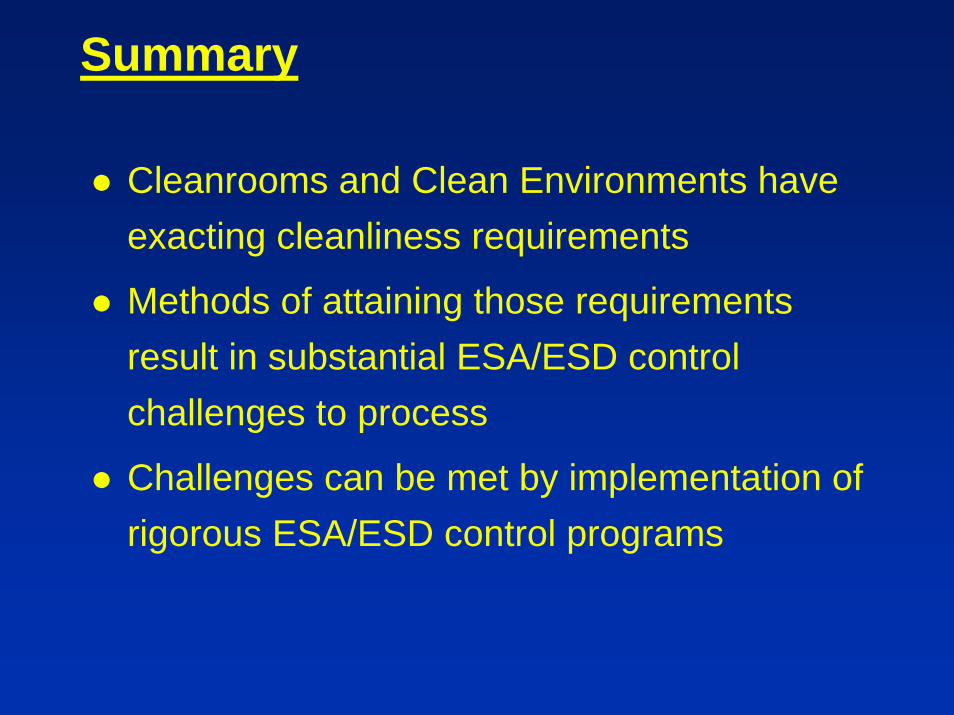
Summary
Cleanrooms and Clean Environments have exacting cleanliness requirements
Methods of attaining those requirements result in substantial ESA/ESD control challenges to process
Challenges can be met by implementation of rigorous ESA/ESD control programs
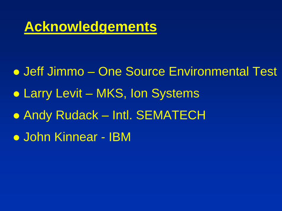
Acknowledgements
Jeff Jimmo – One Source Environmental Test
Larry Levit – MKS, Ion Systems
Andy Rudack – Intl. SEMATECH
John Kinnear - IBM