Embed Size (px)
Citation preview

CHEMICAL SENSOR USING SINGLE CRYSTAL DIAMOND PLATES INTERROGATED WITH CHARGE-BASED DEEP-LEVEL TRANSIENT
SPECTROSCOPY BASED ON THE QUANTUM FINGERPRINT™ MODEL: INSTRUMENTATION AND METHODOLOGY
─────────────────────────────────────────
A Dissertation presented to the Faculty of the Graduate SchoolUniversity of Missouri
───────────────────────────────
In Partial FulfillmentOf the Requirements for the Degree
Doctor of Philosophy
───────────────────────────────
by
DANIEL ENRIQUE MONTENEGRO
Dr. Mark A. Prelas, Dissertation Supervisor
JULY 2011

The undersigned, appointed by the Dean of the Graduate School, have examined the dissertation entitled
CHEMICAL SENSOR USING SINGLE CRYSTAL DIAMOND PLATES INTERROGATED WITH CHARGE-BASED DEEP-LEVEL TRANSIENT
SPECTROSCOPY BASED ON THE QUANTUM FINGERPRINT™ MODEL: INSTRUMENTATION AND METHODOLOGY
Presented by Daniel Enrique Montenegro A candidate for the degree of Doctor of Philosophy And hereby certify that in their opinion it is worthy of acceptance.
───────────────────────── Professor Mark A. Prelas
───────────────────────── Professor Robert V. Tompson, Jr.
───────────────────────── Professor Tushar K. Ghosh
───────────────────────── Professor Sudarshan K. Loyalka
───────────────────────── Professor Dabir S. Viswanath

... if no one will justly lay to my charge avarice or meanness or lewdness; if, to venture on self-praise, my life is free from stain and guilt and I am loved by my friends—
I owe this to my father.
Horace.

ii
ACKNOWLEDGEMENTS
The author would like to express his appreciation and gratitude to his committee
members, Dr. Mark A. Prelas for his unwavering support and mentorship, Dr. Robert V.
Tompson, Dr. Tushar K. Ghosh, Dr. Sudarshan K. Loyalka and Dr. Dabir S. Viswanath
for their much needed guidance and suggestions.
Appreciation is also extended to Latricia J. Vaughn for her invaluable work and
friendship, James C. Bennett for obtaining all those hardware components, and Dr. Jason
B. Rothenberger for his friendship and constant willingness to discuss ideas and designs.
Thanks to other students—past and present— from the Nuclear Science and
Engineering Institute that in different capacities, provided great help to the project. These
include Drs. Lynn and Annie Tipton, Jose Rodriguez, Gwen Chen and Dr. Ryan Myer,
among others.
Appreciation must be given to the organizations and individuals that have supported
this research through generous fellowships or scholarships. These include the Nuclear
Regulatory Commission, the Department of Education, the Defense Threat Reduction
Agency, the University of Missouri’s Graduate School and the John D. Bies Scholarship
Fund.
Finally, the author would like to specially thank his wife, Rebecca, for her love and
encouragement throughout those long hours away from home.

iii
TABLE OF CONTENTS
ACKNOWLEDGEMENTS................................................................................................ ii
LIST OF ILLUSTRATIONS............................................................................................. vi
LIST OF TABLES........................................................................................................... viii
ABSTRACT....................................................................................................................... ix
Chapter
1. INTRODUCTION ........................................................................................................ 1
1.1. Chemical Sensors and Interrogation Methods ..................................................... 1
1.2. Scope of the Research.......................................................................................... 4
2. LITERATURE REVIEW ............................................................................................. 7
2.1. Surface Hydrogenation and Oxygenation Electronic Structures ......................... 7
2.2. Adsorbed Electrolyte Water Layer ...................................................................... 9
2.3. Relationship between surface conductivity and acceptor states in hydrogen- and
oxygen-terminated diamond .............................................................................. 15
2.4. Interrogation Techniques ................................................................................... 16
2.5. Deep Level Transient Spectroscopy: Historical Perspective............................. 17
2.5.1. Development ............................................................................................. 17
2.5.2. Theory ....................................................................................................... 18
2.5.3. DLTS Evolution........................................................................................ 23
2.6. Charge-based Deep Level Transient Spectroscopy Historical Perspective ....... 26
2.6.1. Development ............................................................................................. 26
2.6.2. Theory ....................................................................................................... 30
3. CIRCUIT COMPONENTS AND SOFTWARE CONSIDERATIONS..................... 33

iv
3.1. Circuit ................................................................................................................ 33
3.2. Timing................................................................................................................ 38
3.3. Software-based Double Box-Car ....................................................................... 40
3.4. Data Acquisition ................................................................................................ 41
3.5. Trap Filling Methods ......................................................................................... 43
4. NOVEL SOFTWARE-BASED CHARGE DEEP-LEVEL TRANSIENT SPECTROMETER ..................................................................................................... 48
4.1. Abstract.............................................................................................................. 48
4.2. Introduction........................................................................................................ 49
4.3. Theory................................................................................................................ 50
4.4. Q-DLTS Measurements..................................................................................... 53
4.4.1. Circuit Design ........................................................................................... 53
4.4.2. Timing Signals .......................................................................................... 56
4.4.3. Data Acquisition ....................................................................................... 57
4.4.4. Q-DLTS Algorithm................................................................................... 62
4.4.5. Compensation Methods for Non-Ideal Behavior...................................... 64
4.5. Experimental Details.......................................................................................... 65
4.6. Results and Discussion ...................................................................................... 66
4.7. Conclusions........................................................................................................ 69
5. EFFECT OF VARIOUS MONOHDYRIC ALCOHOLS AND BENZENE DERIVATIVES ON THE ELECTRONIC STATES OF OXYGEN-TERMINATED SINGLE CRYSTAL CVD DIAMOND PLATES ..................................................... 71
5.1. Introduction........................................................................................................ 71
5.2. Theory................................................................................................................ 72
5.3. Experimental...................................................................................................... 83

v
5.4. Results and Discussion ...................................................................................... 86
5.5. Conclusions........................................................................................................ 90
6. FUTURE WORK........................................................................................................ 92
APPENDIX....................................................................................................................... 94
U.S. Patent Office Provisional Patent Application (Modified for consistency) ........ 94
BIBLIOGRAPHY........................................................................................................... 122
VITA............................................................................................................................... 129

vi
LIST OF ILLUSTRATIONS
Figure Page
3.1. Q-DLTS hardware components, a) Circuitry, b) Counter/timers c) DAQ device. .... 33
3.2. Integrating, switching and amplifying circuit. ........................................................... 35
3.3. Flasher circuit output (obtained with a solar cell) vs. triggering pulses of different widths, (a) 5 ms and (b) 6 ms. ................................................................................. 46
4.1. Integrating, switching and amplifing electrical circuit. ............................................. 54
4.2. Timing waveform diagram showing the three counter/timer signals and a characteristic exponential integrator output during a single measuring cycle. The top three waveforms are the voltage signals that control the switching, and Q0 is the integrator output. On the abscissa, tf is the width of the bias pulse, td is the delay width, and T is the period of a single measurement cycle....................................... 56
4.3. Flowchart of the sampling and timing algorithm....................................................... 60
4.4. Flowchart of the Q-DLTS program ........................................................................... 63
4.5. I-V characteristics in a semi-logarithmic scale of the as-received GaN/SiC blue LED structure showing a typical diode behavior............................................................. 66
4.6. Uncompensated spectra showing typical artifacts caused by leakage currents and parasitic capacitance................................................................................................ 67
4.7. Compensated Q-DLTS spectra obtained from the as-received LED sample. Inset shows the Arrhenius trap dependence indicating an activation energy Ea = 0.381 eV, and capture cross-section σ = 1.69 × 10⁻¹⁷ cm2. ............................................... 68
5.1. Energy band diagram of the charge exchange between oxygen-induced traps and the surface electrolyte layer, modified from Ref. [85].................................................. 78
5.2. Diamond sensor with metalized electrodes................................................................ 84
5.3. Testing chamber......................................................................................................... 85
5.4. I-V profile of the oxygen-terminated sensor.............................................................. 85
5.5. Uncompensated Q-DLTS Spectra of oxygen-terminated diamond sensor response to (a) methanol, (b) ethanol, (c) propanol and (d) butanol. ......................................... 87
5.6. Background-subtracted Q-DLTS Spectra of oxygen-terminated diamond sensor response to (a) methanol, (b) ethanol, (c) propanol and (d) butanol. ...................... 88

vii
5.7. Oxygen-terminated diamond sensor response to toluene; (a) uncompensated spectra and (b) background-compensated Q-DLTS spectra................................................ 89
A.1. Hardware diagram..................................................................................................... 94
A.2. Timing profile ........................................................................................................... 95
A.3. Acquisition program flowchart, part I....................................................................... 96
A.4. Acquisition program flowchart, part II. .................................................................... 97
A.5. Acquisition program flowchart, part III. ................................................................... 98
A.6. Q-DLTS filtering flowchart, part I............................................................................ 99
A.7. Q-DLTS filtering flowchart, part II. ....................................................................... 100
A.8. Q-DLTS filtering flowchart, part III. ...................................................................... 101
A.9. Characteristic I-V curve of the unstressed GaN/SiC blue LED.............................. 102
A.10. Q-DLTS spectra of GaN/SiC blue LED, non-compensated for leakage. ............. 103
A.11. Q-DLTS spectra of GaN/SiC blue LED, leakage compensated. Inset: Arrhenius plot......................................................................................................................... 103

viii
LIST OF TABLES
Table Page
2.1. Electron affinity of SC diamond with various surface terminations [14]. ................. 11

ix
ABSTRACT
Semiconductor-based sensors are widely used for the identification of multi-
component chemical and biological mixtures. In recent years, diamond has received a
great deal of interest as a potential sensor material due to its mechanical robustness and
its property to modify its electrical characteristics according to its surface termination and
adsorbed chemical agents. Previous studies have suggested that an adsorbed molecule can
localize a free valency in the same way a surface trap can. The present work focuses on
molecules chemisorbed to the oxygen-terminated surfaces of high-purity CVD single
crystal (100) diamond plates. To investigate the adsorbate-induced surface energy states,
an ultra-sensitive, non-steady state interrogation device called Charge-based Deep-Level
Transient Spectrometer (Q-DLTS) was built and tested. Potentially, a given adsorbed
molecule can be uniquely related to a new surface energy state, thus producing a
characteristic spectral signature. This technology is named Quantum Fingerprint™. The
Q-DLTS system was used to investigate the effect of various monohydric alcohols and
benzene derivatives on the surface states of single crystal oxygen-terminated diamond
plates. It was found that both types of molecules produce a primary large spectral peak
and a smaller, transient one. In the alcohol response, both peaks display a consistent
increase in amplitude (i.e., charge output) as the molecule’s carbon content becomes
larger. The secondary peak also shows a faster emission rate with higher alcohol
molecules. This is attributed to the appearance of new surface states. The secondary peak
of the benzene derivative, however, disappears a few minutes after the initial
introduction. This is believed to be a physisorption effect.

1
1. INTRODUCTION
1.1. Chemical Sensors and Interrogation Methods
The identification of environmental multicomponent biological and/or chemical
mixtures using semiconductor-based detectors is a direction in sensor technology that
recently has received much interest. This is due to their application for homeland
security, port of entry monitoring, military personnel protection and law enforcement
purposes.
Traditionally metal oxide (MOx) films, such as tin dioxide and zinc oxide have been
utilized by measuring their electrical conductivity or resistivity as various gases adsorb to
their active surfaces. Another suggestion made is that this conductivity change is actually
a consequence of an electronic potential barrier change of the grain boundaries in the
metal oxide [1]. The doping of the semiconductor as well as the surface microstructure
and termination are used to control and modify the sensitivity, selectivity and stability of
the sensor. Metal oxides are convenient to use due to their oxidizing stability especially at
high temperatures and their resistance to form permanent covalent bonds to air molecules
that would otherwise reduce the lifespan of the detector. However, this type of detector
does have limitations such as limited selectivity, and the need for heating elements that
become cumbersome for portable applications.
Another type of material that has recently received significant attention is
hydrogenated diamond because it exhibits a low-temperature gas response, a true
negative electron affinity (NEA) and an unusual p-type surface conductivity. The latest
research has shown the almost omnipresence of a surface liquid water layer on its surface
2
which leads to a dissociative gas response due to the formation of a liquid electrolyte
layer. On the other hand, other terminations such as oxygen tend to show positive
electron affinity (PEA) and large ionization potential.
A new modality has recently started to be applied to study the kinetic response
parameters of this material, which promises better resolution and selectivity. These
parameters are obtained after non-steady state methods are applied to the semiconductor
and its excited states are interrogated during relaxation to the quiescent state. This is the
foundation behind Deep Level Transient Spectroscopy (DLTS) and the Quantum
Fingerprint™ sensor technology.
Traditionally DLTS systems have been bulky, cumbersome and expensive. A newer
modality of this technology called Charge-based Deep Level Transient Spectroscopy or
Q-DLTS was developed to mitigate some of these problems by measuring charge (i.e.
current integration) rather than capacitance. This eliminated the need of low- and high-
capacitance meters to measure the carriers’ relaxation process located in the gap states or
deep levels within the depletion region. This technology also inherently removes the loss
of signal amplitude that is dependent on the transient time constant as in conventional
DLTS.
A Q-DLTS prototype has been developed at the Nuclear Science and Engineering
Institute of the University of Missouri. This new development takes advantage of the
emergence of ultra-fast data acquisition devices and effective graphical programming
environments for instrument control. This system does away with all hardware-based data
processing in favor of software-based algorithms. The only essential hardware

3
components are those required to obtain an analog signal output (i.e., raw data) with the
highest possible signal-to-noise ratio.
The Q-DLTS signal processing methodology follows the same DLTS scheme
developed by Lang, which he called dual-gated signal averager or simply double box-car
[2]. The Device Under Test (DUT) is periodically forward biased momentarily to fill the
traps. The DUT is then reverse biased so the traps return to thermal equilibrium with a
time constant directly proportional to their activation energies and amplitude proportional
to their concentrations. The charge is measured at two particular times after excitation.
These times are the rate window gate boundaries. Our system follows the temperature
scan mode in which the rate window is kept fixed and the DUT temperature is scanned to
obtain information related to the traps Arrhenius’ dependence.
The most important breakthrough in our design is the employment of software-based
processing stages after raw data collection. The analog data is sampled at the output of
the integrating amplifier with a fast DAQ device and stored in the PC’s memory. The
digital data is then software-processed in a user friendly LabVIEW environment [3]. This
allows for the possibility of multiple processing/filtering algorithms that can be easily
modified at will. This work will only focus on Lang’s double box-car method, but other
processing methods such as the Gardner transform [4] and the Fast Fourier Transform
(FFT) algorithm are feasible.
The built prototype system has shown very effective in the analysis of wide bandgap
semiconductors such as H- and O-terminated diamond and other more exotic materials
such as AlN [5]. The footprint of the hardware system is minimal, which facilitates
transportation and minimizes construction costs. It is believed that all the aforementioned
4
factors can potentially be applied towards a feasible and profitable system for
employment in research and the semiconductor industry. The response of O-terminated
diamond sensors to both monohydric simple alcohols and monosubstituted benzene
derivatives like toluene indicate a clear and predictable response. In the case of the
alcohols, the longer the carbon chain the greater the Q-DLTS spectrum amplitude. The
emission rates for all the alcohol-induced surface traps are comparable. Toluene, on the
other hand, induces the presence of a short-lived spectrum peak alongside a more stable
one. It is believed that oxygen induces a surface deep-level which, if exited, serves as a
pool of electrons for their exchange with the molecules generated from the adsorbates or
the adsorbates themselves.
1.2. Scope of the Research
The aforementioned technologies were used to study the behavior of diamond films
with different terminations (i.e., hydrogen, oxygen, fluorine, etc.) under different
atmospheric chemical agents. Q-DLTS was utilized to monitor the behavior of the
diamond film to try to find a reproducible behavior. Perhaps, the most important feature
that will be explored—maybe as a proof of concept—is selectivity; that is, the
identification of individual species in the sensor environment by obtaining unique spectra
to each. Next, this behavior will be quantified to find the concentration of molecules
present in the environment. This requires first to have equipment sensitive enough to
detect low-level concentrations; and second, to have a test environment where the
identity and concentration of each molecule in air or vacuum can be fully ascertained.

5
The Q-DLTS approach is utilized almost exclusively for the interrogation of the
sensors. This device was initially based on the system of Arora et al. [6]. The
modifications account for the type of DUT and software-based nature. Since the sensors
generally consist of a semiconducting sensing surface and two electrodes for charge
collection; therefore, it is not required to feed it a negative voltage during the relaxation
part of the measurement cycle, as it would be the case for a p-n junction or a Schottky
barrier. This in some respects simplifies the design because the quiescent ground voltage
level used instead can be directly obtained from the non-inverting node of the integrating
op-amp. Another exception is photo-induced charge measurements; in this case, an
electric field—obtained through a bias voltage—is necessary to sweep the photocarriers
to the electrodes [7]. For this reason, two measurements modes are possible with the Q-
DLTS system presented in this work, i.e., zero voltage bias and variable voltage bias.
This will be described in detail in Chapter 4.
Another modification is the software- based filtering algorithm approach. A
LabVIEW environment will be utilized for this purpose; the LabVIEW toolkit is
particularly suited for this purpose because it contains a variety of specialized algorithms
suited for the in-line analysis and processing of acquired signals [3].
A potential method where different environmental chemical agents can be identified
is by means of a chemical database where the spectrum of the species under test can be
normalized and then compared to those in the database. If a match is found, then further
information can be extracted from the spectrum such as concentration and
adsorption/desorption rates. Maximizing selectivity may require the use of different
filtering techniques to be applied to the obtained exponential transients. This would be

6
imperative if the Q-DLTS spectrum yields closely spaced peaks that cannot be resolved
[5]. In the case where more narrow spectral features are required, then perhaps the double
boxcar filtering can be substituted or even complemented with other spectral fitting
algorithms

7
2. LITERATURE REVIEW
2.1. Surface Hydrogenation and Oxygenation Electronic Structures
Sque et al. investigated the electronic and structural properties of (001) and (111)
diamond with hydrogen and oxygen termination, utilizing ab initio local-density-
functional-theory supercell calculations and software-based analysis [8]. They chose
these particular diamond crystal structures because of their technological importance due
to their ease of production with CVD techniques.
The clean (001) diamond surface (i.e., not terminated) shows neighboring C atoms
joining to form double-bonded dimers with the appearance of occupied π and unoccupied
π* states into the bandgap. These dimers are separated from each other by 2/1 of the
lattice length (i.e., 2.5 Å) forming a nonmetallic (001)-(2×1) surface [8]. On the other
hand the clean (111) diamond surface forms single-dangling-bonds and the upper C
atoms form zig-zag chains running parallel across the surface. These C atoms are
threefold coordinated sharing a delocalized π network forming a (111)-(2×1) semi-
metallic surface [8].
For the (001)-(2×1) clean surface, the double bond induced π and π* states appear in
the forbidden energy gap of the electronic band structure, with the former riding along
the top of the bulk conduction point at the valence-band maximum (VBM). At the
diamond bulk, the value of the Ionization Potential (IP) is Ibulk = 6.11 eV [8]. On the
surface at the maximum of the highest occupied state (analogous to the VBM for bulk)
we have Isurf = 5.85 eV[8]. The conduction-band minimum or CBM is located well below
the vacuum level, and the minimum lowest unoccupied slab state below the CBM. The

8
electron affinity has values of χbulk = +0.64 eV and χsurf = +3.99 [8]. The (111)-(2×1)
clean surface shows an semimetallic electronic band structure with the Fermi level
intersecting the surface states at about 0.8 eV above the bulk VBM and gap states in the
forbidden zone [8]. The aforementioned values for this structure are: Ibulk = 5.83 eV, χbulk
= +0.35 eV and Isurf = χsurf = WF = 5.01 eV [8].
As the most stable structure, the addition of single hydrogen atoms to the (001)-
oriented diamond surface removes the π and π* states from the electronic structure
substituting double to single bonding in the aforementioned surface dimers. On the other
hand, monohydrogenating the (111) diamond surface results in (111)-(2×1):H surfaces
[8]. The bulk energy bands are moved upward by 2.5 eV with respect to the clean surface
due to a low IP and characteristic NEA. In this case the highest occupied state of the
hydrogenated slab is perturbed and lies below the bulk VBM. The ionization potential
values are Ibulk = 3.57 eV and Isurf = 3.97 eV [8]. There are a number of unoccupied states
falling below the bulk conduction band at the VBM point, as much as 2 eV below the
bulk CBM. This latter state may be produced by the p-like orbitals of the C atoms of the
surface dimers and has contributions from both σ C-H bonds and π C-C dimer bonds in a
smaller degree [8]. The surface affinity value is χsurf = +0.24 eV [8]. The next four
unoccupied vacuum states have components along the C-H bond and hydrogenated
dimers. The next higher energy states match almost exactly the states of the bulk system
thus they are due to the bulk-like atoms in the theoretical slab. The affinity of the bulk
has a value of χbulk = –1.90 eV[8]. The electronic structure of the (111)-(1×1):H is
strikingly similar to the previous surface with the following electronic values Ibulk = 3.51
eV, Isurf = 3.71 eV, χbulk = –1.97 eV and χsurf = +0.15 eV [8]. In both hydrogenated

9
surfaces, the band gap states of the clean surface are removed and new unoccupied states
are formed some below the conduction band at the VBM point. The most energetic of
these states exists in the bulk but the few lowest ones are caused by p-orbitals of the
surface carbon atoms with axes along the hydrogen bond [8].
Oxygenating the (001) diamond surface results in two plausible outcomes; a “ketone”
arrangement (i.e., double-bonding a single O atom to a single C surface atom) adopting a
carbonyl-type binding mode on top of the C atom and an “ether” arrangement or linkage
(i.e., single O atom bridging two C atoms making a single bond to each) [8]. Loh et al.
call these the oxygen on top (OT) model and the bridging (BR) oxygen model
respectively [9].
2.2. Adsorbed Electrolyte Water Layer
An early attempt to explain the surface conductivity of hydrogenated diamond
exposed to air was hypothesized by Maier et al.[10]. Under Standard Tempeature and
Pressure (STP) conditions, a hydrogenated diamond surface will absorb a thin layer (~ 1
nm thick) of adsorbed water. Further studies indicated that this effect was also observed
at low-temperature in MOx materials [11]. This was not a surprise since it was already
known that these materials were hydrophilic and thus produced small values in contact
angle experiments.
For the following description, the author will assume that this water layer is neutral,
i.e., it is free from acidic or basic impurities, in other words equal densities of hydroxide
ion and hydronium are present in equilibrium with the water [12],

10
OH¯+OHO2H +32 (2.1)
The neutrality of the aqueous layer may be complicated by the presence of
atmospheric CO2 and its dissolution in water to form hydronium and bicarbonate ions
(i.e., also known as hydrogen carbonate with the chemical formula HCO3¯). The
bicarbonate ions become counterions and the electrolyte becomes mildly acidic rather
than neutral with a PH ≈ 6 [13]. The key ion in the electrolyte is the hydroxide due to its
redox energy level. Charge transfer between the electrons from the diamond valence band
from the bulk and the surface electrolyte can be caused by two different redox reactions
[12],
O2H+H2e¯ ++O2H 223 (2.2)
22 H+2OH¯ 2e¯ +O2H (2.3)
The electrochemical potentials (μ) of these redox reactions are –4.5 eV and –4.0 eV
(respectively) below the electrolytic vacuum level [12]. If considering the value of the
electron affinity of high degree H-terminated undoped (100)-oriented type-Ib diamond
with χ = –1.3 (note the NEA), then the maximum of the diamond valence band
approximately coincides the with energy level of the first redox reaction of the electrolyte
[12].
Unless other mechanism is present, electron transfer can occur from the diamond
valence band to the electrolyte. Both quantitative and experimental data of the value of
different electron affinities of different diamond crystallographic orientations have been
performed throughout the years by several researchers. Robertson and Rutter calculated

11
the affinity of various terminations of diamond surfaces by the ab-initio pseudopotential
method; their results are given in Table 2.1 [14]. Note how the NEA of H-terminated
diamond would be more than enough to induce the said charge transfer.
Table 2.1. Electron affinity of SC diamond with various surface terminations [14].
Surface reconstruction, Calculated electron affinity (eV)2 x 1(100) 0.51
1 x 1(100):2H (sym) -3.191 x 1(100):2H (sym canted) -2.361 x 1(100):2H (asym canted) -2.47
2 x 1(100):H -2.051 x 1(100):O (ketone) 3.641 x 1(100):O (ether) 2.61
2 x 1(100):OH -2.162 x 1(111) 0.35
1 x 1(111):H -2.03
The chemical potential difference of both the electrolyte and the diamond (i.e.,
semiconductor) is responsible for any charge transfer between them. A key parameter is
the chemical potential of the electrolyte related to the semiconductor’s Fermi level.
Nerst’s equation can be used to determine this parameter for any redox reaction
Red
Oxln0 kTcc (2.4)
where 0c can be the initial chemical potential or a standard condition. In our case, the
density of water being constant can be omitted. Then, according to Maier et al., the first
postulated redox reaction using the previous formula can be written as [13],

12
(2.5)
SHE stands for Standard Hydrogen Electrode, which is a type of reference gas
electrode with a pH = 0 and a hydrogen partial pressure of 1.0 atm. Thus, µSHE is the
chemical potential of the standard hydrogen electrode relative to the vacuum level with a
value of –4.44 eV. According to Maier et al., the previous equation can be further
reduced by utilizing the ratio of dissolved hydrogen concentration to its partial pressure
as [13],
2
14.44 0.029 (2 log( )e HeV eV pH p bar (2.6)
Now, for an average atmospheric H2 partial pressure of 1 nbar and pH=6 then we
obtain µe = VBMdia–100 meV and thus there can be charge transfer from the diamond
valence band to the electrolyte. The fact that the diamond’s VBM with a wetting layer is
higher than the electrolyte’s chemical potential is a direct effect of the high NEA due to
the hydrogen passivation [13]. When an electron is transferred from the valence band into
the aqueous solution and the first postulated redox reaction takes place, then a space-
charge region is produced at the diamond-water interface much like that of a p-n junction.
Hydronium molecules and valence electrons are converted into hydrogen, which leaves
unpaired bicarbonate ions (i.e., HCO3─) in the solution. This type of ions is the result of a
dual reaction chain that starts with atmospheric CO2 and water [12]:
-3
+323222 HCO+OHOH+COHO2H+CO (2.7)
23 3
2 2
([ ] /[ ] )/ 2 ln
[ ] /[ ]SHE
e SHESHE
H O H OkT
H H

13
The bicarbonate ions in the electrolyte layer and the holes in the diamond then create
a space charge region, which is self-limited or curved by the electric field it generates.
The space charge density and potential relationship in the diffuse layer of the electrolyte
can be obtained in terms of the electrolyte band bending potential W [13],
02 sinhdiffρ (W) = ec · (W/kT) (2.8)
where c0 is the molecular density of the ionic species in the electrolyte in terms of their
pH value. This value is analogous to the intrinsic carrier concentration of the
semiconductor related to the effective densities of states of the conduction and valence
bands [13]. Note the fact that the asymptotic value of the band bending potential (W0) at
the surface is negative because the chemical potential of the electrolyte was set to zero.
The total charge density can be found by applying Poisson statistics to the previous
equation, obtaining still a function of the band bending potential [13],
))2(sinh(8( 0002kTWckT OHdiff (2.9)
Since equilibrium has been achieved at this point, the diffuse layer in the electrolyte
and the accumulation layer of holes in the semiconductor surface must match. Thus for a
particular hole density and pH value the potential drop or band bending of the diffuse
layer can be obtained in terms of temperature. The electrical potential will increase by
this value above its original position to match the Fermi level of the semiconductor [13].
Though the model presented thus far is fairly accurate to explain the behavior of
hydrogenated diamond surfaces under STP conditions, there are some detractors to this
model. For example, Koslowski et al. observed that surface conductivity is obtained in

14
bulk diamond, epitaxially and homoepitaxially grown CVD diamond (001) films, which
sometimes is orders of magnitude higher than high pressure and high temperature bulk
type-Ib diamond exposed to hydrogen plasma [15]. Their conclusion is that additional
sub-surface hydrogen close to the surface and defects such as grain boundaries may also
play a role in the observed behavior.
Another stumbling block to the Maier et al. model, is the preservation of surface
conductivity under ultra-high vacuum when in fact there is a strong correlation of surface
conductivity and environmental gas composition. Maier et al. relied on the contribution
of carbon dioxide for their model to work, emphasizing the role of HCO3– ions as surface
hole compensators. Szameitat et al. performed a series of CVD diamond surface
conductivity temper experiments under vacuum conditions and under different gas
atmospheres [16]. They reported on the formation of shallow states —and thus easy to
ionize with little activation energy—on the hydrogen terminated diamond, which were
induced by adsorbates. Their samples’ conductivity profile was different whether the
diamond was heated or cooled; showing respectively the effect of bulk charge carries
plus adsorbates and bulk charge carriers alone. After the removal of adsorbates and the
sample returned to atmospheric air the conductivity recovery is slow indicating that the
contributing species are rare in air as in the case of CO2 (0.034% in atmospheric air).
These experiments ruled-out the pronounced effect of this gas to the Maier et al. model.
Kowloski et al. also questioned the relatively step-wise irreversible surface
conductivity collapse above 200 ºC reported by Maier et al. [10, 15]. These researchers
observed that the collapse of surface conductivity has a more complex behavior with
resistance steps at determined temperatures above 200 ºC, no irreversible collapse as such

15
temperature and ultimately a much higher surface conductivity collapse temperature
reported in a series of more detailed analysis.
2.3. Relationship between surface conductivity and acceptor states in hydrogen-
and oxygen-terminated diamond
Since Ristein et al. emphasized the role of atmospheric CO2 in the hydrogen
terminated diamond surface wetting layer with the formation of CO3H─ as the active
solution adsorbate molecule, a component of this work will be in the verification of the
interaction outcome of the latter with the diamond surface [13]. It is not hard to extend
this study to other similar atmospheric molecules that produce an analogous ion in
solution. The author will also refer to the work of Liu et al. that focused in both
hydrogen- and oxygen-terminated CVD diamond samples with a (100) orientation [17].
According to Liu et al., for CO3H─, the band gap between the Highest Occupied
Molecular Orbital (HOMO) and Lowest Unoccupied Molecular Orbital (LUMO) levels is
5 eV; with two positions at the HOMO level of 0.0 eV and –0.64 eV of occupied states
due to the oxygen 2p orbitals [17]. On the other hand, the band gap of the C(100)-2×1:H
surface is clear of shallow acceptors because any surface states induced by C-C π-bonds
(σ bonds are not susceptible to the hydrogen) in the band gap of the bare C(100)-2×1
surface will disappear when the surface is treated with hydrogen [17]. After treatment,
the hydrogenated diamond film shows p-type conductivity, a much lower band gap of 0.8
eV and strong empty surface states above the VBM which act as a trap for valence band
electrons–hence the increased conductivity [17]. The CO3H physisorbed diamond surface
is much different than the clean surface in their band gap profile with a shallow acceptor

16
appearing (0.4 eV) close to the VBM [17]. According to Liu et al. there is an interaction
between the surface C-H bond and non-bonded oxygen 2p orbitals from the CO3H
molecule that lie close to said surface [17].
The oxygen terminated diamond surface exhibits a similar large bandgap (approx.
5.5. eV) than of the bulk, which indicates high resistivity. Loh et al., reporting on the
bridged oxygen configuration (BR), observed a deep and strong valence band state at –22
eV extending to carbon sublayers, which they attributed to the carbon 2p and 2p bonding
orbital induced by the oxygen 2s orbital [9]. Closer to the valence-band-maximum there
are strong surface emission states from 0.0 eV to –2.0 eV originated from the oxygen
non-bonded lone pairs. Density of states calculation also shows states from −4 to 5 eV
and –8 eV from contributions from the O 2p and C 2p bonding orbitals, or rather, CO-like
molecular orbitals. A prominent peak appears at –5 eV below the VBM from
contributions from hybrid O 2p and C 2p orbitals, another CO-like molecular orbital [9].
Finally, a unoccupied state in the conduction band at 4.8 eV is also reported [17].
According to Liu et al. [17], the band gap of the oxygenated diamond surface in
which physisorption of CO3H molecules has occurred, is wide and empty unlike the case
of the hydrogenated diamond and thus it does not produce a similar increased surface
conductivity behavior. At –0.8 eV below the VBM, a new occupied state forms from the
interaction of the CO3H and the CO orbital of the O-terminated surface.
2.4. Interrogation Techniques
Perhaps the second most important component of a chemical or biological sensing
system, apart from the sensing surface itself, is the associated interrogating circuitry. This
17
circuit must accept the signal from the sensing surface, process it and provide an output
to the operator or user. Another necessary step is benchmarking or comparing the
processed signal with known spectra unambiguously related to known agents (in known
concentrations) so the substance that produced the signal can be identified.
If the sensor architecture and mechanism is well understood then the signal collection
should not be difficult provided the appropriate circuitry is utilized. Signal to noise ratio,
shielding, switching, pre-amplification and amplification are parameters that must be
addressed as the output is collected from the sensing surface.
After the signal is received by the circuit and perhaps amplified for the A/D
conversion it must be processed by a separate apparatus. With the advent of high-speed
digital electronics this process can be controlled digitally by a computer and a suitable
development environment such as LabVIEW that supports high-throughput
communication to instrumentation hardware [3]. In such environment, the user can
control the I/O parameters with dataflow programming by means of virtual instruments.
External analog inputs and controls might also be needed to compensate for software
deficiencies. As it shall be extensively described in Chapter 4, the interrogation
technique utilized for the present embodiment of the system is Q-DLTS.
2.5. Deep Level Transient Spectroscopy: Historical Perspective
2.5.1. Development
The original Deep Level Transient Spectroscopy method was devised in the early
seventies by D.V. Lang. While at Bell Labs, Lang was interested in measuring the
capacitance transients due to a shallow ZnO center located about 0.28 eV below the
18
conduction band [18]. At the time, this center was attractive to light-emitting diode
(LED) research because it was responsible of the red photo-luminescence observed in
such devices. However, the somewhat higher temperatures needed for the thermal
emission rate to overcome the slower tunneling rate (dominating at lower temperatures)
would require a very fast recovery capacitance transient measurement circuit, which was
unavailable at the time. In an effort to record these fast capacitance transients Lang
proceeded to adopt a boxcar amplifier or a gated integrator together with a megahertz
bridge circuit. The actual discovery of QDLTS came by rather experimental carelessness.
Lang describes what happened one day while stopping the cryostat which cooled the
sample with the following words [18],
On this day I was distracted for some reason and did not immediately turn off the pulse generators or the boxcar, leaving the gate at a fixed delay relative to the bias pulse. A few minutes later, out of the corner of my eye, I could see the analog boxcar output meter swinging wildly.
When Lang later connected the system’s thermocouple readout to the abscissa of a X-Y
recorder and the boxcar output to the ordinate, he obtained the first DLTS spectrum.
2.5.2. Theory
The original DLTS apparatus was exclusively designed to locate and measure the
deep non-radiative centers on p-n and Schottky junctions [2]. Moreover, Lang’s design
still relied on a megahertz junction capacitance measurement method rather than
stimulated current or thermally stimulated capacitance approaches. Whenever the
occupation of an impurity level from the depletion or space-charge region is subjected to
a non-equilibrium condition it tends to return to the thermal equilibrium state with a
predetermined time constant. According to Lang, “one can measure the time constant of

19
this transient as a function of temperature and obtain the activation energy for the
level”[2]. The non-equilibrium condition is achieved by means of a bias pulse that
introduces carriers that in turn change the steady-state occupation level of the trap center.
Lang identified two principal types of bias pulses whether it produces an increase or
decrease the diode bias. According to Lang [2],
There are two main types of bias pulses, namely, an injection pulse which momentarily drives the diode into forward bias and injects minority carries into the region of observation...and a majority-carrier pulse which momentarily reduced the diode bias and introduces only majority carriers into the region of observation.
In the case of a p-type material, the first type of pulse will increase the electron
occupation of the trap center and thus the capacitance transient will rise above the steady
state or quiescent value. The amount of electrons injected is so great that the minority
carrier capture rate is much larger than the majority carrier capture rate and the traps
cannot empty fast enough so they will fill up with electrons. On the other hand, a
majority carrier pulse will introduce only holes (majority carriers for a p-type material)
into the space charge region sweeping the electrons already filling the majority-carrier
trap and producing a transient decrease in the steady-state junction capacitance [2].
The emission rate values, i.e., the time constant of the capacitance transients, are
controlled by Boltzman statistics of the traps emission and capture rates. Using Lang’s
notation, the quiescent electron occupation of a trap can be thus written as [2],
Nee
eN
cc
cn
21
1
21
11
(2.10)

20
where c1 and c2 are the thermal capture rates of minority and majority carriers
respectively, e1 and e2 are the thermal emission rates of minority and majority carriers
respectively and N is the trap concentration. N can be related to the capacitance transient
after the filling pulse as follows [2],
))(/(2 DA NNCCN (2.11)
where ΔC is the instantaneous capacitance change, C is the quiescent capacitance value
and NA–ND is the net acceptor concentration in the space-charge region (p-type side).
DLTS functions on the basis of adjustable rate window for which the system response
peaks whenever the trap emission rate fits the predetermined rate window. According to
Lang, this emission rate (for a minority carrier) can be written as [2],
)(
11111 )/( kTE
D egNe
(2.12)
where σ1 is the minority-carrier capture cross section, <υ1> is the mean thermal velocity
of minority carriers, ND1 is the effective density of sates in the minority carrier band, g1 is
the degeneracy of the trap level and ΔE is the energy separation between the trap level
and the minority-carrier band. The previous equation of course can apply to majority
carriers by simply changing the subscripts.
Perhaps the greatest achievement of Lang’s invention was to utilize what he called a
“dual-gated signal averager (double boxcar) to precisely determine the emission rate
window and to provide signal averaging capability to enhance the signal-to-noise ratio for
the detection of low-concentration traps [2].” Lang reported a practical rate window
range of 105 – 1.0 sec-1[2]. This is significant because the lower end of the range is

21
considerably fast even for today’s standards. The importance of the double boxcar filter is
that the capacitance difference between the two temporal points of the transient rate
constant will yield a maximum when the capacitance difference at the same two temporal
points is a maximum. The DLTS spectrum yields a well defined peak in the appropriate
temperature axis location whereas in the actual capacitive transient decay it would be
impossible to locate such point [2].
The previous general concept of the double boxcar algorithm serves well to introduce
the reader to a more rigorous definition. The double boxcar has two temporal gates, t1 and
t2. According to Lang [2],
The signal from the differential output of the boxcar is applied to the y-axis of and X-Y recorder. This is simply the capacitance at t1, C(t1), minus the capacitance at t2, C(t2)... this quantity, C(t1)–C(t2), goes through a maximum when τ, the inverse of the transient rate constant, is on the order of t1–t2. Thus the values of t1 and t2 determine the rate window for a DLTS thermal scan.
This sentence has some important definitions, first the transient rate constant or rate
window can be defined as τ–1. Second, the maximum rate window or τmax–1 is the point
where the maximum of C(t1)–C(t2) as a function of temperature is located. Lang went on
to establish the relationship between the normalized DLTS signal (which is simply the
aforementioned capacitance difference between the gate temporal points vs. T) as [2],
]1[)0(
)]()([)( )/()/()/()/(21 121 tttt eeee
C
tCtCTS
(2.13)
where ΔC(0) is the instant capacitance change due to the filling pulse at t=0 and Δt=t2-t1.
Since Lang performed a temperature scan and kept both t2 and t1constant (and thus τ), he

22
was concerned in the value of τ which would yield a maximum of S(T) for a particular
temperature. This τmax can easily be found by differentiating the previous equation:
12121max )]/)[ln(( tttt (2.14)
The DLTS signal in itself is a powerful, but limited, tool to find information about a
particular trap. In other words, the DLTS spectra can be only be used to find trap
concentrations mainly with the aid of the trap concentration equation. However, if the
temperature dependence of the rate window is explored in an Arrhenius plot, then
information such as thermal emission rates and activation energies can be obtained.
As it shall be described later, the Q- DLTS system presented in this work is somewhat
different from Lang’s in the sense that the abscissa temperature scan is substituted by a
rate window scan. In his original paper, Lang suggested this method as the most viable
mode of operation [2]. This observation came after he tried varying one or the other gate
times (i.e., t1 and t2) and noticing that the actual shape of the DLTS peaks would deform
but not when the ratio of these values were kept fixed. The material that Lang utilized for
this experiment was n-GaAs with two minority-carrier (holes) trap levels at 0.44 and 0.76
eV above the valence band with an equal concentration of 1.4×1014 cm–3[2]. Both of
these traps were easily visible in the DLTS spectrum with roughly the same ΔC value,
approximately 200 K apart in the temperature scale and the trap with the higher activation
energy showing a wider peak. As Lang decreased the gate values (keeping their ratio
constant) both peaks showed a right shift towards the higher temperatures. Only five peak
points were enough to construct an Arrhenius plot or a semilog activation energy plot
showing distinctively both activation energies. Finally, Lang proposed methods to
23
establish concentration profiling by means of varying majority-carrier pulse amplitude
and capture rates by means of varying majority-carrier pulse width [2].
2.5.3. DLTS Evolution
In the years following Lang’s capacitance-based DLTS, new methods and devices
were developed. These new systems picked up in areas where DLTS was flawed either
by its intrinsic nature, rigidity of operation or its need of associated devices. For example,
Mahmood et al. pointed out that,“in the extreme limit of high resistivity samples, the
capacitance of the sample may become geometric capacitance at all measurement
frequencies…independent of the charge state of the defect [19].” They also reported on
research made by Tokuda et al. [20], in which GaN samples were subjected to 10 kHz
and 1 MHz capacitance measurement as the sample was cooled to low temperatures. The
measured capacitance after 10 kHz fell to zero due to its time constant. Another problem
is that DLTS might not be suitable to study low concentration states from residual defects
in processed silicon [21].
A couple of years after Lang’s publication, Wessels suggested [22],
…a method for detecting traps based on the combination of the reverse recovery and thermally stimulated current measurements…with this technique, which we call transient-current spectroscopy, both the trap energy and capture cross-section can be independently determined for majority- and minority-carrier traps.
The essence of Wessels’ transient-current spectroscopy (ITS) method did not deviate that
much than that of Lang’s; i.e., the measurement of transients (current in this case) from
deep-levels inside the depletion region of p-n junctions or Schottky barriers due to the
thermally stimulated emission of its carriers. Wessels was interested in determining traps

24
in vapor-phase epitaxy grown GaP doped with nitrogen, sulphur and most importantly,
copper. The p+ doping (i.e., for p+-n junctions) was obtained by zinc diffusion [22].
The diode’s excitation method is also similar to Lang’s. The current transient is
measured for about 10 ns at time t1 after the excitation pulse trailing edge; using Wessels’
nomenclature, this transient can be written as [22],
e
t
e
eWqAtN
I
1
2
)((2.15)
where N(t) is the filled trap density, q is the electron elementary charge, A is the junction
area, ΔW is the change of depletion region width and τe–1 is the trap emission rate. If this
equation is differentiated as a function of the latter, then a maximum transient current is
observed at τe=t1; that is, if the inverse sampling gate time is equal to the trap emission
rate then this corresponds to a peak in the spectrum which is associated to a characteristic
temperature.
Wessels also claimed the possibility of finding the trap energies and the temperature
dependence of the emission rates by varying the gate delay time t1 and quantifiying the
spectrum pike(s) shift. The corresponding equation was given as [22],
kT
EI
e
T
eg
Nt
11
1 (2.16)
where NI is the effective density of states, σ is the capture cross-section, <υ> is the carrier
mean thermal velocity, g is the trap level degeneracy and ΔET is the trap energy level.
This equation is significant, thus it shall be repeated more or less in the same
configuration in further papers. The reason for its significance is that by plotting its

25
variation on a semi-logarithmic Arrhenius plot (i.e., emission rate vs. inverse of
temperature) then the traps energy levels can be obtained. Wessels was able to find this
way the three well-defined peaks on his Cu-doped GaP diode ITS spectrum and match
them to three hole traps with energy levels of 0.5 eV, 0.62 eV and 0.82 eV [22]. Other
parameters such as trap concentration and capture cross sections can also be obtained
with the aid of variables such as injection pulse width.
In 1980, Borsuk and Swanson [21] developed a DLTS system similar to Lang’s but it
measured current —rather than capacitance—transients like Wessels’. Their system was
a somewhat cumbersome apparatus, using correlator and calibration outputs coupled to
the diode output. According to Borsuk and Swanson [21],
Consider a p+-n diode. The diode bias is pulsed between a small reverse bias Vf, during which electron traps fill, and a larger reverse bias, during which the depletion width widens and trap emission is measured. As electrons are emitted, )/exp()( 0 eTT tNTn , where nT is the
concentration of trapped electrons, NTO is the concentration of filled traps immediately before the voltage is switched from Vf to Vm, and τe is the emission time constant.
The aforementioned voltages are the diode bias voltages that are supplied during injection
and relaxation respectively. For the previous definition it is important to point out that the
authors were only interested in majority-carrier emission and they assumed that the trap
concentration was much lesser than the donor concentration. According to Borsuk and
Swanson, the variation of the occupancy levels of the traps (i.e., emission of carriers from
the space-charge layer) causes a capacitive response given by [21],
21
2
)(2
)]([)(
mbi
STD
d
S
VV
AtnNq
W
AtC
(2.17)

26
where A is the junction area, Wd is the depletion width during relaxation and Vbi is the
junction built-in voltage. Alongside the capacitive response there is a current response
given by [21],
L
t
e
TOLT
e
IeqWAN
ItnqWA
ti e
2)(
2)( (2.18)
where IL is steady-state diode leakage current during relaxation and W is the width of the
measurement volume.
2.6. Charge-based Deep Level Transient Spectroscopy Historical Perspective
2.6.1. Development
In 1981, Kirov and Radev [23] in an effort to understand the interface states and bulk
traps of semiconductor materials (in particular MIS capacitors on a n-type substrates)
developed a charge-based DLTS technique based on Lang’s original design. According to
these authors regarding the measurement of interface states on MIS capacitors [23],
The measurement procedure is the same as for the C-DLTS technique. A quiescent reverse voltage UG, is applied to the gate, so that the structure is in deep depletion. For a short time a forward biased, filling pulse is superimposed, resulting in accumulation and filling of the interface states with electrons. A new non-equilibrium depletion condition is established after the filling pulse. Due to thermal emptying of the interface states their charge, QSS, will change. This leads to a change in the capacitance of the structure and simultaneously to a change in the gate charge. By the C-DLTS method the first effect is used. We propose that the second one, i.e. the change in the gate charge should be measured.
For p-n junctions and Schottky barriers the aforementioned change of charge takes the
following form [23],

27
2tnqW
Q
(2.19)
where W is the width of the depletion region and nt is the concentration of electrons
captured by the total concentration of centers (Nt). According to these authors, this
concentration can be described by [23],
ttt eNn
(2.20)
where τ is the time constant of the exponential depletion of the traps given by [23],
cthn
kTE
N
et
(2.21)
where Et is the trap energy level from the conduction band edge, σn is the electron capture
cross-section, υth is the electron thermal velocity and Nc is the effective density of states
at the conduction band.
The principle of operation of Kirov and Radev’s apparatus is to connect a known
capacitance (C) in series with the DUT. C is composed of the actual DUT capacitance
and any other parasitic capacitance from the cabling, apparatus, etc. The former will be
periodically charged by the DUT with a charge that is proportional to ΔG and this signal
will be amplified by an electrometer. Whenever the charging capacitor and DUT are not
connected to the amplified they will be connected to ground. The connection of the
charging capacitor to the amplifier begins at time t1 and ends at t2, therefore the DUT
charge change between these times is [23],

28
)(2
)(21
12
ttt ee
qWNttQ
(2.22)
According to the authors, the apparatus also has an RC1 low-pass filter to reduce any
frequency higher than the switching frequency or noise not synchronized with the
switching frequency [23]. The requirements of this filter are that RC1 >> T and C << C1.
If these requirements are met, then the voltage input to the amplifier can be described as
[23]
)1( RCTC
QV G
I
(2.23)
The breakthrough of Kirov and Radev’s design was its simplicity and sensitivity (the
authors stated a minimum interface-state densities resolution of 2×10⁸ eV–1cm–2) when
studying high resistivity materials [23].
In 1982, Farmer et al. independently developed another charge-based DLTS
apparatus based on Lang’s design; that is, that the diode was kept reverse biased except
during brief moments during which it was fed a pulse voltage towards zero bias [24].
After this excitation, the trapped carriers within the space-charge region will be thermally
emitted causing the reduction of the depletion width. Farmer et al. started out by
considering the relaxation junction current given by [24],
2)(
)/( tT eAqWN
ti
(2.24)

29
where all terms were previously defined. The decay time constant can be further
described as in Wessels’ work minus the degeneracy factor. According to Farmer et al.
this current can be electronically integrated as follows [24],
t t
T eAqWNdttitq
0
/
2
)1(')'()(
(2.25)
These authors were careful to point out that the removal of the τ–1 prefactor benefited this
method over I-DLTS for large values of τ. The integration was performed by a simple
operational amplifier with a parallel RC feedback network. This is a very widely utilized
circuit (see for example Ref. [25]) that simply converts an input current into an output
voltage. According to Farmer et al. this voltage can be described by [24],
)(2
)()(
//
RC
eeRAqWNtV
tRCtT (2.26)
or, in the case of a large RC time constant, as
C
tq
C
eAqWNtV
tT )(
2
)1()(
/
(2.27)
These authors were prompt to note the presence of two input current signals that will
be integrated along with the DUT signal. The first are large current spikes resulting from
the diode capacitance with approximate integrator output amplitudes of CCV d /
where ΔV is the filling pulse amplitude and Cd is the diode geometric capacitance. This
large pulse is the result of indiscriminate integration alongside the true signal and it must
be suppressed for proper operation. Farmer et al. used a simple sample and hold amplifier
30
for this purpose [24]. The second input current signal—and that of most frustration in the
author’s own experiments—is the presence of leakage signals from the DUT. This type of
leakage current has three main characteristics: it is constant, small—when compared with
the traps signals—and it depends on the value of the voltage level during quiescence or
de-excitation. For a diode, this value is due to the reverse-biased voltage; for other
samples such as a solar cell or a sensor it may be due to an operational amplifier’s offset
voltage. Farmer et al. further obtained a leakage-current error expression, which indicated
a reduction of this error by keeping the period of the pulse train large and the bias pulse
width small [24]. The leakage current problem will be further addressed later as well as
appropriate algorithms designed to minimize it.
Farmer et al. utilized their device to analyze the trap profile of neutron irradiated n-
type silicon. Since they utilized a fixed-gate timing scheme the two chosen gate times
were 10 μs and 100 μs. The RC value of their integrator was 20 ms. Three defects levels
were found in their sample with densities of 8.9×1014 cm–3, 7.0×1013 cm–3 and 9.3×10¹⁴
cm–3 with energies of 0.16 eV, 0.22 eV and 0.43 eV respectively [24]. The latter values
were found by the use of Arrhenius plots from temperature scans from 83 K to 333 K.
2.6.2. Theory
The last journal on the particulars on Q-DLTS that will be reviewed, is the work of
Arora et al. [6]. Since the in-house system is loosely based on this design, its theory will
be reviewed in this section in detail. In Lang’s algorithm, the rate window was user-
defined and constant while the temperature was increased at a constant rate. Since the
thermal emission rates are strongly dependent on temperature this thermal scan would
resolve the peaks that fell within the range of the rate window. An analogous algorithm

31
proposed by Arora et al., is to maintain the sample temperature constant while the rate
window is varied [6]. In other words, assuming a constant ratio of gate times t2/t1=α
(throughout this work α = 2 but different values are possible) the difference of the values
or t2–t1 can be varied.
Following the same reasoning as Lang’s but applied to charge rather than
capacitance, the gate timed charge difference emitted from the beginning of discharge is
simply,
)()( 12 tQtQQ (2.28)
If an exponential behavior of the charge emission is assumed, then the previous
equation can be also written as
)( 210
tete nn eeQQ (2.29)
where, as before, en is the inverse of the electron (from donor-like traps in this case but it
can also correspond to hole or acceptor-like traps) emission rate constant and Q0 can be
described as
0
0 )( dttQQ (2.30)
According to Polyakov et al. [26], the emission rate constant can be described
(similarly to Eq. 2.13) as,
kT
E
nn
a
eTe 2Γ (2.31)

32
where σ is the capture cross section, T is the temperature, Ea is the activation energy, k is
the Boltzmann constant and Γn can be defined as,
nn mkh 22/322/1 )/2(32 (2.32)
where h is the Planck constant and mn is the effective mass of the electron (or hole if
appropriate).
According to Arora et al. a maximum in the spectrum will occur when the rate
window equals the emission rate of the trap for a particular temperature [6],
)()1(
ln
1
Tet n
(2.33)
and substituting for α = 2 we have
)(/2ln 1 Tet n (2.34)
Substituting this value back in Eq. 2.29 we have
4/0max QQ (2.35)
The previous equation is significant because it directly allows a calculation from the
actual spectral peaks of the total charge collected from the DUT.

3. CIRCUIT COMPONENTS A
3.1. Circuit
As in Lang’s original design
excite the deep-centers and traps and observing the electron
returns to thermal equilibrium.
in favor of adaptable software
components (see Fig. 3.1)
emitted trapped charge transients, provide the timing signals that control each
measurement cycle and to sample and process the raw data.
Figure 3.1. Q-DLTS hardware components, a) Circuitry, b) Counter/timers c) DAQ device.
33
CIRCUIT COMPONENTS AND SOFTWARE CONSIDERATIONS
As in Lang’s original design, Q-DLTS relies on cyclic bias pulses to momentarily
ers and traps and observing the electron occupation of the level as it
returns to thermal equilibrium. This system foregoes all hardware-based data processing
software-based algorithms. The only necessary electronic
(see Fig. 3.1) are those essential to amplify and integrate the thermally
emitted trapped charge transients, provide the timing signals that control each
measurement cycle and to sample and process the raw data.
DLTS hardware components, a) Circuitry, b) Counter/timers c) DAQ
ATIONS
ulses to momentarily
occupation of the level as it
based data processing
only necessary electronic
essential to amplify and integrate the thermally
emitted trapped charge transients, provide the timing signals that control each
DLTS hardware components, a) Circuitry, b) Counter/timers c) DAQ
34
As shown in Fig. 3.2 the most prominent feature of the circuitry is the integrator
circuit composed of op-amp U1. This state-of-the-art device is a National Semiconductor
Ultra Ultra-Low Current Amplifier model LMC6001 [27]. According to the device
datasheet [28], this device guarantees input currents of 25 fA max., virtually noiseless
amplification (if care is taken with surrounding circuitry as well) to high resistance DUTs
and very low input offset voltage. Furthermore, this device was explicitly designed for
electrometer applications for sensor applications.
The output of this circuit is directly proportional to the charge emitted by the centers
during the emission process during relaxation. In reality, this charge is a current that is
integrated by the any of the user-selected capacitors C1 – C4. Assuming no leakage
currents, the voltage at the output of the integrator can be described as
0'
0 int
DUTout
)'(Vdt
C
tIV
t
(3.1)
where Cint is any of the integrating capacitors, IDUT is the sample output current and V0 is
the integrator output voltage at t = 0. Taking out the constant terms we have,
0'
0
DUTint
out d)'(1
VttIC
Vt
(3.2)
and noting the relationship between electric current and charge (i.e., I = –dQ/dt) and
assuming V0 = 0 we obtain the relationship between the charge of the integrating
capacitor and the output voltage of the integrator itself,
intout
)(
C
tQV (3.3)

Figure 3.
35
.2. Integrating, switching and amplifying circuit.. Integrating, switching and amplifying circuit.

36
The aforementioned current (Eq. 2.25) was given before in the works of Farmer et
al.[24]; however, these authors utilized an RC network rather than just a purely capacitive
network in the feedback path. However, they arrived at the same equation (see Eq. 2.28)
by assuming an RC constant much larger than the current transient decay constant of the
sample. At the output of the integrator there is also a gain stage composed of resistors R7
and either of R1 – R6 forming an inverting amplifier circuit with a ideal gain of
7
6:1
R
RA (3.4)
Thus the previous equation becomes,
intout
)(
AC
tQV (3.5)
One of the biggest hurdles of the design was the appropriate selection of switching
relay RL1. This relay carries the low-level signal from the DUT to the integrator and
switches its conduction path twice per charging cycle. Since usually the DUT signals are
so small, the choices in the appropriate switching device are somewhat restricted. When
currents fall in the nanoampere region these switching problems are magnified. As it can
be seen in Fig.3.2, two switching points are required, the switching of the DUT itself (i.e.,
RL1) and the integrator reset switch (i.e., U4a). The latter is utilized to discharge the
appropriate integrating capacitor during the filling pulse part of the cycle (see next
section) so the integration can start during relaxation. These switches encompass the two
types available: an electromechanical relay (reed type) and a solid-state (i.e.,

37
semiconductor) switch. Rako explains the problem with the latter when dealing with
small currents and an integrating circuit reset switch [29],
Using a semiconductor switch is impractical due to leakage currents and the 5 – 20 pF capacitance most analog switches offer. The capacitance exhibits a varactor effect as well; it changes with applied voltage, further complicating measurements.
The use of solid-state switches for integrator circuit resetting applications is not
uncommon though; for example, both the ACF2101 and IVC102 are precision low-noise
switched integrators that feature internal solid-state reset switches [30]. Device U4a,
shown in Fig. 3.1, is a MAX326 quad, SPST CMOS-based solid-state analog switch [31].
This device features a 10 pA maximum leakage current (1 pA typical) and low charge
injection (2 pC typical). The latter is produced due to the parasitic capacitance between
the gate and source/drain inputs of any MOS device and of course it depends on the size
of the device [32]. The error produced by the leakage current is perhaps more significant
than the charge injection. This error would become significant when the DUT current
approaches the order of magnitude of the leakage current.
Experiments performed with both analog and electromechanical switches led to the
use of the latter for the DUT switching. Following the example given by Rako, it was
decided to utilize a reed relay model 9852 1-Form-C (i.e., SPDT), which features an
external magnetic shield, a coaxial shield and an insulation resistance of 1012 Ω min
[33]. Furthermore, its coil’s inductance is suppressed by both a Zener and standard diode
combination. Electromechanical relays do not suffer from leakage currents—as long as
the device’s case is kept clean so surface currents are insignificant—or charge injection
errors; however, they are limited in terms of switching speeds. The aforementioned relay
has a typical operate—including bounce—and release time of 0.3 ms (1.0 ms max.) [33].
38
This speed would be untenable if a standard hardware-based double box-car approach is
performed by the circuitry. However, as it shall be seen later, in the present algorithm, the
correlation will be performed by the software after the raw data (i.e., collection of the
trapped charge) is digitally stored in the computer memory. This allows for a single scan
per filling pulse where all the information required for a full QDLTS spectrum is
contained. Of course, multiple charge collection scans might be preferable to obtain a
charge output average for a particular temperature and rate window value. If we assume
that the charge of the fast relaxing centers is not dissipated during the operate time of the
reed contact of the relay, then we can set a delayed time for the beginning of the
integration after the switch has closed (i.e., DUT is in contact with the inverting input of
the op-amp) and all switching transients have decayed away.
3.2. Timing
The device utilized for timing purposes is a USB-4301 5-channel, 16-bit, high-
performance 9513-based counter/timer device from Measurement Computing™ [34]
shown in Fig. 3.1.(b). According to the manufacturer’s datasheet [35],
The USB-4301 is a USB-based high-performance, low-cost counter/timer device…designed with a 9513 counter/timer chip. The 9513 chip has five independent 16-bit counters (65,536 counts). Each counter has an input source, internal count register, load register, hold register, output, and gate. The 9513 is software-programmable for event counting, pulse and frequency measurement, alarm comparisons, and other input functions. The 9513 can generate frequencies with either complex duty cycles, or with one-shot and continuous-output modes…The gate source and gating functions are software-programmable. An eight-bit, high-current digital output port provides logic-level control, and can be used to switch solid state relays. An eight-bit digital input port can be used to sense contact closures and other TTL level signals.

39
The main component of the USB-4301 is the USB Microcontroller that connects to a PC
via a full-speed USB interface (USB 2.0 compliant). The microcontroller is internally
connected to a clock generator that can provide four different base frequencies (i.e.,
1.0000, 1.6667, 3.3333 and 5.0000 MHz) to the five independent counters. The base
frequency can be chosen one at a time with a manufacturer’s provided software utility
called InstaCal [36]. This utility can be also utilized to configure the triggering edge
parameters. Once the appropriate base frequency is chosen it can be further divided in
five lower frequencies in multiples of 10. For example, if a base frequency of 1.6667
MHz is initially chosen, then any of the counter/timers can be configured with internal
frequencies of 1.6 MHz, 166.67 kHz, 16.667 KHz, 1.6667 kHz and 166. 67 Hz.
As it can be seen in Fig. 4.2, the circuit relies on two triggering signals; the second
signal (TRIG2) is delayed by a user-defined amount of time, usually in the microsecond
range. Although not expounding on it, Arora et al. mentioned the need for the monitoring
of the charge signal after an initial delay time to “avoid the unwanted initial transient”
[6]. This transient is produced both by the associated circuitry and the DUT itself. For
example, the switching relay will produce an inductive “kick” at the switching instant.
According to Rako, describing an experiment that required the use of reed relays[29],
… you can also look at a reed relay as a transformer, with the reed relay as a transformer, with the reed assembly representing a single turn. This phenomenon explains the failure of electrostatic shield to prevent the interference. Magnetic fields inducing voltages in the high-impedance side of the circuit caused the charge injection. The relay does not open instantaneously, and the pulse needed to energize the coil makes a significant current injection just before the relay opens.
On the other hand, there is transient belonging to the intrinsic capacitance of the DUT;
Thurzo and Grendel referred to this initial transient as the “charge increment ΔQ0, related

40
to the instantaneous (geometrical) capacitance of the device: Cg=ΔQ0/ΔU” [37]. This
transient component should be much larger than the steady-state charge from the trapped
charge emission and would saturate the integrator if care is not rendered to its removal.
Other initial transients are inherent to the switching of the DUT, from the bias pulse node
to the integrator input node. Because of these two transient behaviors, it would be
inappropriate to start the integration process at the switching instant. Rather, a small time
delay should be applied to avoid the integration of potentially large voltage spikes that
would otherwise saturate the output. This delay however, cannot be too long so the
trapped charge due to fast emission rate processes is lost trough some form of leakage
mechanism. Typically this delay is adjustable where an appropriate value can be chosen
after visual inspection of the pre-filtered output signal.
The circuit timing profile can be seen in Fig. 4.2. The first positive square signal is
the reference signal that is produced by the first counter of the USB-4301 device via
terminal OUT1. This counter is internally gated and serves to establish the cycle period
and also as a reference for the two utilized circuit triggers (i.e., TRIG1 and TRIG2). Each
cycle period must be long enough for all the trapped charge to be collected and
integrated, especially those from slow decaying processes. This period is usually in the
range of hundreds to thousands of milliseconds.
3.3. Software-based Double Box-Car
An essential part of Q-DLTS (or any DLTS algorithm) is choosing the appropriate
filtering of the total transient charge. The filter chosen for the present application is a
derivation of the first-order DLTS filter proposed by Lang which he called a dual-gated

41
signal averager or double boxcar [2].The particulars of this algorithm were described
earlier. Higher order filters are also possible as well; for example, Thurzo and Gmucová
[38] proposed a second-order filter based on the work of Crowell and Alipanahi [39], that
would remove any constant component of the total released charge. Other transient
analyses have been described. These include, among others, a nonlinear double
exponential fitting routine to analyze digitally recorded capacitive transients [40], linear
regression by the method of least squares [41], multi-exponential analysis based on a
non-linear least-squares analysis [42], spectral analysis or SADLTS [43] and various
methods of discrete Fourier analysis [44, 45].
3.4. Data Acquisition
The first attempt to collect the raw data (i.e., integrated current or total collected
charge) was performed with a USB-6009 low-cost multifunction USB-based data
acquisition card (DAQ) from National Instruments™ [46]. This particular DAQ featured
a maximum sampling rate of 48 kS/s with an analog input (AI) resolution of 13-bits if
using a single-ended configuration. This device also features an analog input First-In
First-Out (FIFO) buffer of 512 bytes to hold the data during the A/D conversion. The
USB-6009 also features a configurable dedicated digital trigger (Programmable Function
Interface input or PFI) for the AI task. This trigger can be configured either for a negative
or positive digital edge (coming from the USB-4301 counter/timer) to start the
acquisition of the amplified integrator output signal.
The somewhat slow sampling rate of the previous device (i.e., 20.8 μs in-between
sampled points) would introduce aliasing for output frequencies faster than the Nyquist

42
frequency of the device (i.e., 24 kS/s or 41.7 μs between sampled points). Thus, if the
time constant of centers of fast thermal emission rates are higher than this value its
trapped charge emission profile cannot be reconstructed. One of the two known
commercial Q-DLTS systems is called the Automatic System of Material Electro-
Physical Characterization (ASMEC) manufactured by InOmTech [47]. The ASMEC
model-06 features a quoted range rate window of 3×10⁻⁶ – 200 s [48]. Therefore to
approach and exceed this fast rate window we would need a DAQ that can sample at least
at 2 × 333 kHz = 667 kHz. A fast and uniform sampling rate is useful for the fast
transient components of the collected charge; however, transients with long time
constants would not benefit from fast sampling rates. As a matter of fact, their digitized
conversion would consist mostly of irrelevant data due to oversampling. Additional
problems are the additional memory required to store such amount of data and the
possibility of an undersized buffer. A solution proposed by Doolitle and Rohatgi is to
decrease the sampling rate as the time constant of the single transient’s exponential
components increases [49].
The current state of high-speed electronics, however, allows for faster sampling rates
and buffers with increased memory storage. The author’s second attempt at fast data
sampling was using a M-Series USB-based multifunction DAQ model USB-6221 also
manufactured by National Instruments [46]. This device , shown in Fig. 3.1.(c), has
multiple AI with an A/C resolution of 16 bits and a maximum sampling rate of 250 kS/s.
This is not enough to match the ASMEC-06 initial rate window values, but at least it can
accurately resolve transients with time constants higher than 20.0 μs. The device has
multiple PFI inputs (with debouncing filters) that can serve as digital triggers for the AI

43
task, although only one is required. The input FIFO buffer size is 4,094 samples or 512
bytes; this is the same size as that of the USB-6009 DAQ device.
3.5. Trap Filling Methods
The two ways of trap excitation (i.e., to change the charge state of the centers by
introducing carriers) are voltage and light. The former was utilized by Lang to introduce
these non equilibrium conditions [2]. Lang went further in carefully describing the two
types of bias pulses which would introduce either majority or minority carriers into the p-
n junction. These pulse sequences differed on whether they momentarily drove the diode
into forward bias or not, but both regiments required a steady-state negative DC voltage
during the relaxation part of the cycle (i.e., between filling pulses) to maintain the diode
reverse biased. In the present case since the planar electrodes from symmetrical ohmic
contacts on the surface of the diamond film the reverse biasing would have been
unsuitable for the application. The negative voltage during quiescence was then replaced
for a zero voltage or ground effected by the virtual ground property of the integrating op
amp. As it can be seen in Fig. 3.2 the non-inverting node of the op amp is not directly
connected to ground but it has a small voltage to deal with the non-ideal input offset
voltage. Since the other side of the chip is connected to ground; care must be rendered
that this ground connection is as close as possible to the integrating op amp.
The non-equilibrium filling voltage pulse is originated in the R13 (Fig. 3.2) multiple-
turn potentiometer. The resistive element terminals are connected to the –15 V and 15 V
supplies to provide negative and positive pulses. Originally only the switching relay was
utilized to alternate the connection of the DUT from the potentiometer (first part of the

cycle) to the integrator (second part of the cycle). However, the common terminal of the
switching relay (for experimental purposes disconnected fr
fast exponential decay behavior at the lowering edge of the pulse rather than a well
defined vertical edge. This decaying voltage would unavoidably be integrated and
saturate the op amp if any part of it lay after the delay time.
Figure 3.3. Decay transient due to the filling pulse.
To help avoid this decaying behavior another switching step is provided by the
analog switch (i.e., MAX326). The switch will
the switching relay during the
the analog switch are much faster than the relay there is no danger of timing interference;
that is, the switching timing is still controlled by the relay.
The other excitation method
tube. These types of light sources are widely used in photography
inexpensive and easy to find.
and the broad white light spectrum produced
shown in Fig. 3.4. Although seemingly complicated
44
(second part of the cycle). However, the common terminal of the
switching relay (for experimental purposes disconnected from the DUT) experienced a
fast exponential decay behavior at the lowering edge of the pulse rather than a well
defined vertical edge. This decaying voltage would unavoidably be integrated and
saturate the op amp if any part of it lay after the delay time.
Figure 3.3. Decay transient due to the filling pulse.
To help avoid this decaying behavior another switching step is provided by the
analog switch (i.e., MAX326). The switch will open the path from the potentiometer to
the switching relay during the relaxation part of the cycle. Since the operating times of
the analog switch are much faster than the relay there is no danger of timing interference;
that is, the switching timing is still controlled by the relay.
method is a light pulse from a photon source such as a xenon
of light sources are widely used in photography, thus they
easy to find. Other benefits of xenon tubes are the large pho
and the broad white light spectrum produced. The circuit utilized for this purpose is
Although seemingly complicated, this circuit has only a few main
(second part of the cycle). However, the common terminal of the
om the DUT) experienced a
fast exponential decay behavior at the lowering edge of the pulse rather than a well
defined vertical edge. This decaying voltage would unavoidably be integrated and
To help avoid this decaying behavior another switching step is provided by the U4
the path from the potentiometer to
relaxation part of the cycle. Since the operating times of
the analog switch are much faster than the relay there is no danger of timing interference;
source such as a xenon
thus they are
the large photon density
utilized for this purpose is
this circuit has only a few main

components. The two transformers are responsible for increasing a small DC voltage with
a large current (i.e., 1.5 V from a standar
current. Transformer T1 is responsible for charging the
of approx. 300 V. The combination of resistor
battery forms a feedback oscilla
triggering signal itself had not enough current output to energize the coil of the relay (i.e.,
83 mA min.) Thus, the transistor provides the necessary current, while the trigger is
connected to the base.
The charging voltage will also be fed to the primary coi
will provide the voltage (
secondary coil. The C1/R
to emit light whenever the charging voltage reaches the required voltage.
voltage will momentarily ionize the xenon gas inside the tube and decrease its
45
components. The two transformers are responsible for increasing a small DC voltage with
(i.e., 1.5 V from a standard AA battery) into a large voltage with a small
is responsible for charging the electrolytic capacitor to
The combination of resistor R1, transistor Q1, transformer
battery forms a feedback oscillator. The 13003 PNP transistor Q2was added because the
triggering signal itself had not enough current output to energize the coil of the relay (i.e.,
min.) Thus, the transistor provides the necessary current, while the trigger is
Figure 3.4. Optical pulse/flash circuit.
voltage will also be fed to the primary coil of transformer
provide the voltage (usually in the low kilovolts range) to the trigger node with its
R3 network is a time delay circuit that will cause the neon lamp
to emit light whenever the charging voltage reaches the required voltage.
ntarily ionize the xenon gas inside the tube and decrease its
components. The two transformers are responsible for increasing a small DC voltage with
into a large voltage with a small
capacitor to a voltage
1, transformer T1 and
2was added because the
triggering signal itself had not enough current output to energize the coil of the relay (i.e.,
min.) Thus, the transistor provides the necessary current, while the trigger is
l of transformer T2, which
usually in the low kilovolts range) to the trigger node with its
3 network is a time delay circuit that will cause the neon lamp
to emit light whenever the charging voltage reaches the required voltage. The trigger
ntarily ionize the xenon gas inside the tube and decrease its

impedance. This will provide a path for the charge stored in the
cause additional ionization and a bright light emission until the capacitor is drained.
value (10 µF, 315 V) of the
charge in less than a second.
Figure 3.3. Flasher circuitdifferent widths, (a) 5 ms and (b) 6 ms
Fig 3.4 (a) shows the trigger pulse compared with the actual flash
output) obtained with a silicon
connected directly to the Ch. 2 of the oscilloscope. The figure shows an approx. 2.5 ms
delay between the falling
can be attributed mainly to the operate time of
46
impedance. This will provide a path for the charge stored in the C2 capacitor, which will
cause additional ionization and a bright light emission until the capacitor is drained.
of the charging capacitor was experimentally chosen to obtain a full
charge in less than a second.
er circuit output (obtained with a solar cell) vs. triggering pulses of , (a) 5 ms and (b) 6 ms.
shows the trigger pulse compared with the actual flash output
silicon solar cell (Model 276-124 from Rasdioshack
directly to the Ch. 2 of the oscilloscope. The figure shows an approx. 2.5 ms
delay between the falling edge of the trigger pulse and the outset of the flash. This delay
can be attributed mainly to the operate time of the switching relay of the flash circuitry.
2 capacitor, which will
cause additional ionization and a bright light emission until the capacitor is drained. The
experimentally chosen to obtain a full
output (obtained with a solar cell) vs. triggering pulses of
output (i.e., light
sdioshack [50])
directly to the Ch. 2 of the oscilloscope. The figure shows an approx. 2.5 ms
the flash. This delay
of the flash circuitry.

47
The flash itself lasts about 3.0 ms. Thus, a trigger pulse of ~ 6.0 ms should be sufficient
to start the integration of a photo-sensitive chip’s transient output without interference of
the flash itself, which causes the excitation of the traps. Fig. 3.5 (b) shows the effect of a
6 ms pulse. Note that this time, the rising edge of the pulse exceeds the falling edge of the
light output.

48
4. NOVEL SOFTWARE-BASED CHARGE DEEP-LEVEL TRANSIENT
SPECTROMETER
4.1. Abstract
Presented is a novel Charge-based Deep Level Transient Spectroscopy (Q-DLTS)
system for the characterization of semiconductor materials. This straightforward design
takes advantage of the emergence of fast data acquisition cards, and effective graphical
development environments. This system foregoes all hardware-based data processing in
favor of adaptable software-based algorithms. The only necessary electronic components
are those essential to amplify and integrate the thermally emitted trapped charge
transients, and to provide the timing signals that control each measurement cycle. The
software program then digitally filters the raw data, compensates for spurious input
signals and produces a Q-DLTS spectrum based upon user-defined input parameters. This
device was used to analyze the traps occurring in blue GaN/SiC light-emitting diodes.
The study indicated the presence a minority-carrier trap occurring at a discrete energy
below the conduction band with an apparent activation energy Ea = 0.381 eV, and a
capture cross-section σ = 1.69 × 10⁻¹⁷ cm2. It is considered that this level is originated
from a deep Mg-VN donor complex.

49
4.2. Introduction
One of the most widely utilized methods for characterization of the deep-level centers
in semiconductors is deep-level transient spectroscopy or DLTS. First proposed by D.V.
Lang, this technique is based on the measurement of junction capacitance transients due
to thermal emission during a thermal scan; however, conventional DLTS suffers from
inherent setbacks [2]. For example, if the series resistance of the Device Under Test
(DUT) is large, the capacitance transient may vary with the measurement frequency. If
the resistivity is large enough, the capacitance transient might approximate the geometric
capacitance for all measurement frequencies [51]. For heavily doped materials,
capacitance spectroscopy suffers from poor sensitivity [52]. Furthermore, systems using a
capacitance bridge for measurement are inherently slow, which limits its usable range to
traps above an activation energy of 0.1 eV [53].
Alternative measurement schemes have been proposed over the years. Some of these
methods rely on the direct measurement of thermally stimulated current transients, or the
integration of these currents to yield charge transients (Q-DLTS) [22, 24, 54, 55]. Most of
these systems rely on hardware-based timing mechanisms to perform the required DLTS
signal processing. Computer systems that perform such functions have been proposed but
they are generally cumbersome or difficult to build [56]. This chapter describes an
apparatus that is a combination of a relatively simple circuit structure, and software-based
signal processing algorithms used to obtain a Q-DLTS emission spectrum and a
quantitative spectrum analysis. This configuration takes advantage of the advent of high-
speed data acquisition (DAQ) devices and ever faster computer processor speeds. The

50
device was used to study the carrier density of blue GaN/SiC Light Emitting Diodes
(LEDs).
4.3. Theory
As in Lang’s original dual-gated signal averaging or DLTS method [2], the Q-DLTS
technique relies on cyclic bias pulses to momentarily excite the traps of p-n junctions and
Schottky barriers. The electron occupation of a level is monitored as it returns to thermal
equilibrium by measuring the associated charge transients. In this scheme, a rate window
is defined as a function of two measuring gate times (t1 and t2) starting at the beginning of
the trap discharge. The charge transient is measured at these two times and the difference,
Q(t2)–Q(t1), is plotted as a function of temperature. According to Maxwell-Boltzmann
statistics, the thermal emission rates are strongly dependent upon temperature. At a
particular temperature, a thermal scan will produce an emission rate that matches the rate
window. Therefore, a peak in the spectrum occurs because Q(t2)–Q(t1) is maximized. If
several emission rates are present, then multiple peaks appear.
If the time-dependent trap distribution is assumed to be uniform then the thermally
stimulated current can be described as [24],
T
TT
tAqWN
ti
2
exp
)(
(4.1)
where A is the junction area, q is the elementary charge, W is the junction depletion
width, NT is the trap density, and τT is the trap decay time constant. To obtain the charge
emitted, the previous equation must be integrated over time,
51
T
Tt
o TT
Tt tAqWN
dttAqWN
dttitQ
exp12
exp20
(4.2)
The prefactor in Eq. (5.2) is the total charge collected,
20
0TAqWN
dttiQ
(4.3)
Traditionally in DLTS, the rate window or τ -1 is kept constant while the temperature
is varied. A similar method is to maintain a constant temperature while the rate window is
varied [55]. This rate window can be described as a function of the ratio of the gate times
(i.e., t2/t1=α) as,
112
121
1
lnln
ttt
tt
(4.4)
Similar to Lang’s algorithm, the gate timed charge difference emitted from the beginning
of discharge is simply,
21 tQtQQ (4.5)
For electrons, the previous equation can be also written as,
210 expexp teteQQ nn (4.6)
where en is the electron emission rate, which has the form [57],
kT
ETe a
nn exp2 (4.7)

52
where σ is the capture cross-section, T is the temperature, Ea is the activation energy, k is
the Boltzmann constant, and Γn is defined as,
nn mkh 22/32/232 (4.8)
in which h is the Planck’s constant and mn is the effective mass of the electron. The
equations for holes are analogous. For a given temperature, a maximum in the spectrum
will occur when the rate window equals the emission rate of the trap. This can be easily
verified by differentiating Eq. (6), which yields,
1 1
1
ln
1T net
(4.9)
Substituting for α=2 into Eq. (5.9) (which corresponds to the present design) we have,
1/2ln ten (4.10)
Substituting this value back into Eq. (6) we obtain,
4/0max QQ (4.11)
Eq. (11) is significant because it allows a direct calculation of the total charge collected
from the Q-DLTS peak maxima. Finally, because of the Arrhenius dependence of the
emission rate, the values of σ and Ea can be calculated using Eq. (7). Although not
investigated in this paper, further averaging algorithms such as nth Order Filtering,
Fourier-based Multi-Exponential DLTS and the Gardner transform are possible, and even
desired.[58-60]

53
4.4. Q-DLTS Measurements
4.4.1. Circuit Design
Fig. 4.1 shows the current integration circuit used to obtain the DUT charge output
[25]. The overall system diagram is shown in Fig. A.1 in the Appendix. An LMC6001
ultra-low current amplifier from National Semiconductor was utilized for this purpose
[61]. The input bias current of the device can be compensated with a simple voltage
divider circuit. For proper circuit behavior, leakage currents must be controlled;
especially at low input currents. Shield and guard rings can be utilized to reduce leakage;
however, it is better to have none of the terminals associated with the pre-amplified input
signal in contact with the printed circuit board (PCB). Using air wiring and enclosing the
circuitry in a shielded enclosure minimizes leakage, electrostatic interference and noise
due to airborne ions impinging on the integrating capacitors [29]. If care is taken with the
hardware components and correction algorithms are employed to overcome non-ideal
circuit behavior (i.e., charge injection, parasitic capacitive coupling, electronic noise,
etc.) then the sensitivity range of the system can be extended into the femto-coulomb (fC)
region. As it can be seen in Fig. 4.1, the maximum total gain of the present system is
Av,max ≈ 274 dB, thus a charge input of Qin = 100 fC would yield a voltage output Vout =
0.5 V. The high sensitivity capabilities of the system are evident in the low ΔQ values of
the spectra shown later in the work.

Figure 4.1. Integrating, switching and amplifing
The switching mechanism
design. It needed to be fast enough
sampled without signal degradation. A
switching charge injection needed to be minimized
were unsuccessful due to the large commutation noise and slow operating times. Solid
state analog switches based on CMOS technologies with sub
and low charge injection
as the integrator reset switc
The low-noise amplifier of the second gain
general purpose operational
nulling capability [61]. This feature
integrator reset stage and null
54
Integrating, switching and amplifing electrical circuit.
mechanism proved to be the most challenging part of the circuit
needed to be fast enough that the fast thermal emptying transients
without signal degradation. At the same time, fast transients associated with the
switching charge injection needed to be minimized. Several experiments with reed relays
ere unsuccessful due to the large commutation noise and slow operating times. Solid
state analog switches based on CMOS technologies with sub-picoamp leakage current
ection proved more successful [31]. A similar device was also utilized
the integrator reset switch that controls the sampling/integration cycle.
noise amplifier of the second gain-stage provides additional gain. The
erational amplifier used for this purpose must have built
This feature can be utilized to zero-out the output during the
integrator reset stage and null any jump caused by the switching charge injection
circuit.
enging part of the circuit
fast thermal emptying transients could be
time, fast transients associated with the
experiments with reed relays
ere unsuccessful due to the large commutation noise and slow operating times. Solid
picoamp leakage current
device was also utilized
the sampling/integration cycle.
ides additional gain. The
built-in offset
out the output during the
switching charge injection [29].

55
If the DUT is a p-n or Schottky diode then a reverse bias or quiescent voltage (VB) is
required during the relaxation part of the measurement cycle. In this Series Mode, switch
Q1 (see Fig. 4.1) is kept open, and the bias pulse is generated from one of the DAQ
Analog Outputs (AO). This analog waveform must be externally triggered by the
reference signal (REF in Fig. 4.2), and offset by VB during the relaxation part of the
measurement cycle. The analog bias pulse width (tc) is then configured to have the same
length as the delayed switching signal (i.e., tc = tf +td). As in Lang’s DLTS method, two
types of momentary filling or bias pulses are possible: a saturating injection or forward
bias pulse, which injects minority carriers into the depletion region and a majority carrier
or reverse bias pulse, which introduces majority carriers into the depletion region.
The DUT filling voltage (∆VB) can also be provided by a voltage divider shown in
Fig. 4.1 at the front end of the circuit diagram. This Parallel Mode configuration was
designed to probe the surface states of semiconductor-based sensors with symmetrical
electrodes deposited on the sensing surface [53]. Another method for deep-level states’
excitation that is particularly suitable for this configuration is with a light pulse; this
technique has been previously called Photoinduced Current Transient Spectrometry or
PICTS [62]. If this method is used, then care must be taken to match the bias pulse length
(tf) to the light pulse width.

Figure 4.2. Timing waveform diagram showing the three counter/timer signals and a characteristic exponential integrator output during a single measuring cycle. The top three waveforms are the voltage signals that control the switching, and output. On the abscissa, tf
period of a single measurement cycle.
4.4.2. Timing Signals
Three counters/timers
controls the period of the
all the long-lived trapped charge transients to decay away.
checking—with an oscilloscope or a recurrent voltage vs. time plot
plateauing of the total charge collected
point in this region. In the
counter/timer device from Measurement Computing
versatile 9513 counter/timer chip, which has
65,536 maximum counts)
internal clock generator; thus
magnitude different. For example, the reference signal period can be as long as a few
56
. Timing waveform diagram showing the three counter/timer signals and a characteristic exponential integrator output during a single measuring cycle. The top three
he voltage signals that control the switching, and Q0 is the integrator tf is the width of the bias pulse, td is the delay width, and
period of a single measurement cycle.
/timers are needed to produce the timing signals. The reference signal
controls the period of the excitation/discharge cycle. The period must be long enough
lived trapped charge transients to decay away. This can be done by visually
an oscilloscope or a recurrent voltage vs. time plot—for a flattening or
plateauing of the total charge collected, and ensuring that the next cycle starts at some
point in this region. In the present design the REF signal is obtained via a USB
r/timer device from Measurement Computing [34]. This device is base
versatile 9513 counter/timer chip, which has five independent 16-bit counters (i.e.,
). All the counters are dependent on a single configurable
thus, they cannot be used to output time events that
. For example, the reference signal period can be as long as a few
. Timing waveform diagram showing the three counter/timer signals and a characteristic exponential integrator output during a single measuring cycle. The top three
is the integrator is the delay width, and T is the
reference signal
. The period must be long enough for
can be done by visually
for a flattening or
ng that the next cycle starts at some
a USB-4301
based on the
it counters (i.e.,
. All the counters are dependent on a single configurable
to output time events that are orders of
. For example, the reference signal period can be as long as a few
57
seconds but the forward bias pulse width can be in the microsecond range. For this
reason, another separate counter/timer chip is required. Incidentally, the USB-6221 M-
Series DAQ device from National Instruments used for the data acquisition has two 32-
bit independent counters that can be utilized for this purpose [46]. These were used to
generate the undelayed and delayed switching signals (i.e., SIG1 and SIG2 respectively)
using the period signal as a trigger source. The adjustable delay (td) of SIG2 is added to
avoid the integration of the aforementioned switching transients.
The value of td must be chosen carefully because its associated error (φd) is a function
of the fastest charge transient present in the DUT (τT). Experiments with several
resistor/capacitor (RC) networks with various time constants yields the following error
formula,
971.0762.0exp1 Tdd t (4.12)
Experimentally, without a priori knowledge of τT, a delay of 3.0 µs was usually effective
to cancel out both the switching transients and parasitic coupling effects, while causing a
delay error of less than 5.0% for traps emission rates of time constants slower than 50 µs.
4.4.3. Data Acquisition
The analog-to-digital (A/D) conversion and timing section is illustrated in the
flowchart of Fig. 4 3. The program first configures the task of producing the
charge/discharge cycle trigger pulse train (i.e., the REF waveform). After this, the DAQ
device counting tasks are initialized and configured. The internal outputs of the two
device counters produce the SIG1 and SIG2 waveforms. The three signals are produced

58
indefinitely and continuously until all sampling cycles are completed and the sampled
data is stored in the PC memory.
The sampling rate of the de-excitation transient must be fast enough so even the
fastest thermal emissions can be processed by the Q-DLTS algorithm. This can only be
accomplished if the sampling rate (fs) and the initial and final values of the rate window
array (τ0 and τf respectively) obey two constraint equations. The first equation is
001 log^10log^10ln If s (4.13)
where I is the logarithmic rate window interval defined by
0 flog logI
n
(4.14)
and n is the desired number of points on the abscissa of the Q-DLTS spectrum. Each
value of the rate window array can be calculated with the following equation,
iIi 0log^10 (4.15)
It is easy to verify that the subtraction terms of Eq. 5.13 correspond to τ1 and τ0,
respectively. Because we are dealing with discrete values, the inverse of the sampling
rate cannot be lesser than the difference of the first two user-selected values of t1. For
simplicity, the right side of Eq. 13 is called D in Fig. 4.4. The second constraint equation
is
N
f fs
ln1 (4.16)
59
where N is the total number of sampled points. The numerator in Eq. 16 corresponds to
the largest value of t2, thus the equation forces this value not to exceed the last sampled
data point. Since extrapolation is unfeasible in these ranges, the highest rate window and
its associated t2 value are the main reason for unused data. For simplicity, the right side of
Eq. 15 is called E in Fig. 4.4. The maximum sampling rate of the DAQ device is fs,max=
250 kHz; therefore, the values of τ0, τf and n must be chosen accordingly.

Figure 4.3
60
3. Flowchart of the sampling and timing algorithm.Flowchart of the sampling and timing algorithm.

61
The Analog Input (AI) task is set up by first creating an analog input channel to
measure voltage. Then, the user-defined sampling rate is configured by setting the source
of the sample clock. Finally, the triggering for the task is configured using the delayed
switching signal (SIG2) as the trigger source. The start, read and stop parameters of the
task are located inside a loop. Similar steps are performed for the AO task. Each filling
pulse is associated with a unique transient decay curve that is averaged after each cycle.
The resulting data is stored in an array that is carried from one iteration to the next via
shift registers. The Signal-to-Noise Ratio (SNR) can be significantly improved by
increasing the number of iterations (NI). After the preset number of iterations is reached,
the averaged data array is stored in the PC memory and a plot is generated.
The software communicates with the DAQ card via a single Universal Serial Bus
(USB) port. This data transfer protocol was chosen so the system would maintain its
portability by allowing the use of a laptop PC. Traditionally however, external buses such
as USB have suffered from poor latency and low bandwidth. To ensure high-speed
bidirectional analog data transfer over USB, the chosen DAQ device features several
advanced technologies. The data acquisition is hardware-timed and buffered; that is, the
data is transferred from the DAQ’s 12-bit First In/First Out (FIFO) buffer to a data buffer
in the PC memory. The DAQ device has two dedicated Input/Output (I/O) onboard Data
Memory Access (DMA) channels—among six that are incorporated into the card’s
Advanced Timing Controller. DMA data transfers free the computer processor’s
resources to execute other data operations [63]. USB latency is greatly improved with NI
Signal Streaming technology [64]. During the initial data request, the host computer
sends a single high-level message that is interpreted and converted by the DAQ device

62
processor itself, into the appropriate register-level commands to configure the system and
timing controller.
As previously mentioned, an oscilloscope can be used (and indeed encouraged) for
qualitative purposes to visually inspect the shape of the raw DUT charge output;
however, the type of data manipulation previously described cannot be obtained just with
a stand-alone oscilloscope. Some of these reasons are that the sampling rate, number of
sampled points, etc., must be variable and user-defined; and multiple measurement cycle
averaging is usually required. Therefore, a digitizer or DAQ device with high data
throughput and sampling rate, and ease of automation is essential.
4.4.4. Q-DLTS Algorithm
The program illustrated in Fig. 4.4 essentially executes the algorithm described in the
theory section. The first notable addition is the calculation of the points on the spectrum
abscissa or τ-axis; which, following the convention in the literature, has units of log(μs).
The parameter input sequence is inside a loop structure to ensure that the sample rate
constraints (i.e., Eqs. 5.13 and 5.16) are met. If this is not achieved, the program prompts
the user to reenter all or some of the values.

Figure
63
Figure 4.4. Flowchart of the Q-DLTS program

64
The amplitude or charge output array is first smoothed by the mean displaced ratio
(MDR) method [65], and then digitally filtered via a Butterworth low-pass filter. This
filter was chosen due to its small frequency response characteristics; however, other types
of filters are possible. Knowing I, n and τ0 allows the program to calculate each pair of t1
and t2 values by linear interpolation from the time array. The corresponding charge values
are then linearly interpolated from the amplitude array, which was previously converted
to units of charge (pC). Finally, the spectrum is plotted and the data is stored in the PC’s
memory. The Q-DLTS peaks are calculated by grouping sequential data points in arrays
of equal user-defined lengths. Each group of data points are fit into quadratic polynomials
and then differentiated twice to obtain each peak’s amplitude, location and sharpness.
4.4.5. Compensation Methods for Non-Ideal Behavior
A typical Q-DLTS uncompensated spectrum will show the presence of several non-
ideal spectral features. Most notably, the junction’s temperature-dependant leakage
current under reverse bias is unavoidably integrated alongside the charge output of the
DUT, and appears as an exponentially increasing charge at the tail end of the spectrum.
This behavior can be partially hardware-compensated with a bias resistor as shown in
Fig.5.1; in addition, two software leakage suppression methods are possible. If the
leakage is integrated and digitized from the diode under reverse bias, then this data set
can then be subtracted from the total charge output. An alternative algorithm is to obtain
the slope of the curve of the leakage vs. time, then artificially create an integrated leakage
current array and subtract it from the total charge output array. An alternative algorithm
is to calculate the slope of the curve of the leakage vs. time after all transients attributed
to carrier emission have decayed away. Since the leakage is constant, the slope is then

65
used to artificially create an integrated leakage current array that is subtracted from the
total charge output array.
Another non-ideal spectral feature accentuated at low trap concentrations are peaks
associated with coupled parasitic capacitance (i.e., from coaxial cabling, circuitry, etc.)
and charge injection. These usually appear as fast isothermal narrow peaks. An easy
compensation method is as follows. For a given peak, the Q-DLTS spectrum yields
information of both the total charge output (i.e., Eq. 5.11) and the transient time constant
(i.e., Eq. 5.9). Therefore, these parameters can be used to artificially generate an identical
charge data array—to that produced by the parasitic capacitance—and subtract it from the
total charge output. Another option is to use the delay time feature; however, this option
is valid only for capacitive coupling whenever its time constant is faster than the fastest
trap emission time constant.
4.5. Experimental Details
The apparatus was utilized to study the acceptor levels present in commercial low
brightness GaN/SiC blue LED structures [66]. Group-III nitrides LEDs have been
extensively studied in the past in terms of failure modes, degradation and aging
mechanisms [67-70]. The photoluminescence in the blue spectral range is obtained by the
incorporation of Mg acceptor impurities, which results in p-type doping [71]. Nitrogen
vacancies (VN) are also formed during the GaN growth with similar concentrations of that
of the Mg acceptor [72].
The LED structures were of the form of square dices (0.0136 × 0.0136 mm2) mounted
p-side up on ceramic stems and encapsulated in epoxy resin. For the present study, four

LED junctions were placed in parallel to increase the
DLTS measurements were carried out using the following parameter values:
VB = –1.0 V, tc = 20 ms, t
This particular saturating injection pulse voltage, which matches the GaN bandgap, was
chosen to reveal the minority
measurements were performed over a
increments of ~7 K.
Figure 4.5. I-V characteristics in a semiblue LED structure showing a typical diode behavior.
4.6. Results and Discussion
The characteristic I-V
confirms the presence of a
spectrum of the as-received LED device. The graph shows the presence
66
LED junctions were placed in parallel to increase the deep centers’ charge output.
DLTS measurements were carried out using the following parameter values:
td = 0 µs, T = 200 ms, NI =100, Av = 226 dB, and
This particular saturating injection pulse voltage, which matches the GaN bandgap, was
chosen to reveal the minority-carrier traps (i.e., donor levels) present in the structure. The
measurements were performed over a temperature range of 256–296 K measured in
characteristics in a semi-logarithmic scale of the as-received GaN/SiC blue LED structure showing a typical diode behavior.
esults and Discussion
V curve of the unstressed sample at room temperature (
confirms the presence of a p-n junction. Fig. 4.6 shows the uncompensated Q
received LED device. The graph shows the presence of a typical
centers’ charge output.[68] Q-
DLTS measurements were carried out using the following parameter values: ∆VB = 3.5 V,
and fs = 250 kHz.
This particular saturating injection pulse voltage, which matches the GaN bandgap, was
carrier traps (i.e., donor levels) present in the structure. The
296 K measured in
received GaN/SiC
curve of the unstressed sample at room temperature (Fig. 4.5)
6 shows the uncompensated Q-DLTS
of a typical

isothermal capacitance peak at
with the measurement of the main peak under test. Leakage effects, on the other hand, are
significant, and must be compensated for the peak
Fig. 4.7 shows the compensated spectrum.
Figure 4.6. Uncompensated spectra showing typical artifacts caused by leakage currents and parasitic capacitance.
67
isothermal capacitance peak at τ ≈ 50 μs; however, its small amplitude does not interfere
with the measurement of the main peak under test. Leakage effects, on the other hand, are
significant, and must be compensated for the peak-finding algorithm to function properly.
7 shows the compensated spectrum.
. Uncompensated spectra showing typical artifacts caused by leakage currents and parasitic capacitance.
50 μs; however, its small amplitude does not interfere
with the measurement of the main peak under test. Leakage effects, on the other hand, are
algorithm to function properly.
. Uncompensated spectra showing typical artifacts caused by leakage currents

Figure 4.7. CompensatedInset shows the Arrhenius trap dependence indicating an activation energy and capture cross-section
The filling pulse must
charge saturation are reached. This procedure is performed during the setup stage and at
low temperatures by increasing
spectrum. In samples with strong leakage currents, however, any long
buried by the integration process regardless of the correction algorithm employed.
expected, the position of the visible single dominant peak shifts to shorter ti
as the temperature is increased. From the Q
(inset of Fig.5.7) to calculate the values of the trap
eV, and capture cross-section
found in the literature for similar LED structures
68
Q-DLTS spectra obtained from the as-received Inset shows the Arrhenius trap dependence indicating an activation energy
section σ = 1.69 × 10⁻¹⁷ cm2.
must be long enough to assure that a quasisteady state and full trap
charge saturation are reached. This procedure is performed during the setup stage and at
low temperatures by increasing tc until no further long-lived peaks appear in th
spectrum. In samples with strong leakage currents, however, any long-lived peaks will be
buried by the integration process regardless of the correction algorithm employed.
expected, the position of the visible single dominant peak shifts to shorter ti
as the temperature is increased. From the Q-DLTS spectra, an Arrhenius plot was used
7) to calculate the values of the trap apparent activation energy
section σ =1.69 × 10⁻¹⁷ cm2. These values closely match those
found in the literature for similar LED structures [67, 69]. In particular, a state of similar
received LED sample. Inset shows the Arrhenius trap dependence indicating an activation energy Ea = 0.381 eV,
be long enough to assure that a quasisteady state and full trap
charge saturation are reached. This procedure is performed during the setup stage and at
lived peaks appear in the
lived peaks will be
buried by the integration process regardless of the correction algorithm employed. As
expected, the position of the visible single dominant peak shifts to shorter time constants
DLTS spectra, an Arrhenius plot was used
activation energy Ea = 0.381
closely match those
In particular, a state of similar

69
activation energy has previously been associated to a deep Mg-VN donor center [73]. This
complex is formed when a Mg acceptor associates with an oppositely charged nearest-
neighbor nitrogen vacancy at high Mg doping levels [72]. This complex, together with a
Mg shallow acceptor, participate in a donor-acceptor pair (DAP) transition that has been
shown to be responsible for the well-documented 2.8 eV blue photoluminescence band at
room temperature [72].
4.7. Conclusions
A novel software-based Q-DLTS instrument and method to characterize the surface
and bulk deep states in semiconductor materials was described. The novelty of the design
lies in its modularity capabilities, high sensitivity and simplicity. Its construction only
requires a low-noise integration amplifier circuit with fast switching capabilities, a high-
speed DAQ device, three counter/timers, and a PC running a suitable programming
language. With this instrument, the user has full data control during all stages of
measurement; from the initial post-sampling raw data to the final Q-DLTS spectrum the
data can be visualized and analyzed. All the required constraint and sampling parameters,
error analysis and programming details were described in the paper.
A vital component of the system is the software-based Q-DLTS algorithm. In
previous publications, this algorithm has been implemented by hardware components, or
by more complicated pseudo-logarithmic storage schemes. The dual-gated signal
averaging or other data processing schemes, and the compensation for non-ideal circuit
behavior are performed post-sampling by the software. High SNRs can be obtained by
multiple averaging and low-pass filtering of the digitized data. This does not translate
70
into longer processing times because the time spent by traditional DLTS hardware
circuits in repetitive measurement cycles of increasing length is entirely avoided. Instead,
the algorithm speedily obtains the desired emission spectrum based on user-defined
parameters. Although the theory of DLTS or Q-DLTS is not new, similar instruments
available commercially and those described in the literature were, in our view, lacking in
essential features.
The device described in the paper was used to characterize the deep-levels present in
commercial GaN/SiC blue LEDs. A single deep-level was found, with an apparent
activation energy Ea = 0.381 eV and capture cross-section σ = 1.69 × 10⁻¹⁷ cm2. The
sample temperature range was 256 – 296 K. This energy level is attributed to a deep Mg-
VN donor complex. The blue luminescence band has been attributed to a DAP transition
from this deep donor to a Mg shallow acceptor.

71
5. EFFECT OF VARIOUS MONOHDYRIC ALCOHOLS AND BENZENE
DERIVATIVES ON THE ELECTRONIC STATES OF OXYGEN-TERMINATED
SINGLE CRYSTAL CVD DIAMOND PLATES
5.1. Introduction
Semiconductor-based sensors are widely used for the identification of environmental
multi-component chemical and biological mixtures. Traditionally, metal oxide (MOx)
films, such as tin dioxide (SO2) and zinc oxide (ZnO) have been the preferred materials
used for these applications. The doping of the semiconductor as well as the surface
microstructure, topology and termination are utilized to control and modify the
sensitivity, selectivity and stability of the sensor [74]. The sensing method is conductance
or resistance modulation, or the measure of the change of the electrical conductivity or
resistivity as gases adsorb to their active surfaces. The sensing mechanism responsible for
these changes has been variously attributed to changes in the surface carrier density [75],
changes in the electronic potential barrier in the grain boundaries or changes in the
concentration of surface unsaturated oxygen adsorption sites [1]. Metal oxides are
convenient to use due to their oxidizing stability—especially at high temperatures—and
their resistance to form permanent covalent bonds to air molecules that would otherwise
reduce the lifespan of the detector. However, this type of detector does have limitations
such as limited selectivity (usually up to a couple of chemicals per sensor type) and the
need for heating elements that become cumbersome for portable applications. On the
other hand, diamond has received much interest as a potential sensor material due the

72
change to its electrical properties caused by surface termination and atmospheric
adsorbates [76].
5.2. Theory
Hydrogenated diamond exhibits a low-temperature gas response, a true negative
electron affinity (NEA) and an unusual p-type surface conductivity [77]. To explain this
behavior, researchers have postulated the effect of an almost omnipresent adsorbed thin
water layer on the surface, which leads to the formation of a liquid electrolyte layer [10].
In this model, electron exchange occurs from the diamond surface to the aqueous layer.
Another model calls for the presence of a sub-surface acceptor layer with nearly constant
space charge density in between the surface and the diamond bulk [78]. Oxygen
termination, on the other hand, tends to show positive electron affinity (PEA) and large
ionization potential [8]. This paper will only focus on adsorbates chemisorbed to the
oxygen- and hydrogen-terminated surfaces of type-IIa ultra-high purity CVD diamond
(100) plates [79]. The principal reason for this choice is that its band-gap is relatively free
of bulk states. Thus, if surface states are present they can be directly attributed to the
chemisorbed species. The appearance of these surface states also induces the change of
the position of the Fermi level, the buildup of band bending, and the modification of the
ionization energy of the semiconductor [80].
Hall Effect measurements on hydrogen-terminated CVD polycrystalline diamond
indicating high carrier concentration and mobility in the surface region have been linked
to surface and near-surface hydrogen induced acceptor states [81]. Further studies on
intrinsic hydrogen terminated CVD diamond films have also suggested the appearance of

73
an insulating separation layer and the formation of additional adsorbate-related charged
states [82].
The effect of chemisorption on semiconductor on the system of surface states is not
new; in 1966 Wolkenstein postulated a “strong” form of chemisorption whenever a free
valency—electron or hole—of the surface is involved in the binding of the chemisorbed
particle [83]. Thus, the adsorbed particle can localize a free valency in the same way a
surface trap can. In this model, chemisorbed chemicals induce new recombination centers
and/or alter the electrical parameters of those already present at the surface. The new trap
centers can be either a donor or acceptor depending on the nature of the adsorbed particle,
and subsequently they modify the surface electronic band structure. Another similar event
can also occur, i.e., if particles adsorb on acceptor or donor defects already present on the
surface. These new levels will have the same nature as the native surface defects but will
have different energy levels.
Wolkenstein’s “weak” chemisorption was described as one that does not involve an
electron or hole in the crystal. In this case, electrostatic forces are involved when the
deformation of electronic orbitals is caused by the electron clouds of either the adsorbate
or surface crystal being drawn to one another. This effect is purely quantum-mechanical
since the chemisorbed particle becomes polar while maintaining its neutrality. At any
rate, the new dipole moment is always larger than that induced by physical adsorption or
physisorption. The latter only induces electrostatic-type forces (i.e., van der Waals, etc.).
Whatever the case may be, these new centers will be populated by carriers; and
therefore, they will modify the magnitude and sign of the charge state of the surface. The

74
sensing area-normalized number of charged particles chemisorbed (i.e., charged
chemisorption) can be described as (using Wolkenstein’s nomenclature) [83],
kTNN S
exp0 (5.1)
where the negative sign—only on N—corresponds to acceptor particles and the positive
sign corresponds to donor particles, N0 is the amount of adsorbed particles under
adsorption equilibrium (i.e., neutral chemisorption), εS is the location of the Fermi level at
the surface (the negative and positive signs corresponds to the distance from the
conduction and valence bands respectively), υ is the location of the chemisorbed particle-
induced surface state (again, the negative and positive signs corresponds to the distance
from the conduction and valence bands respectively), k is the Boltzmann constant and T
is the temperature. It is evident from the previous equation, that introducing factors that
can change the location of the Fermi level (e.g., impurities) to the semiconductor crystal,
its response to chemisorptions can be modulated.
Since chemisorbed particles changes the surface charge, then band-bending and a
Fermi level shift occurs; this, in turn, changes the work function and electrical
conductivity. The latter effect is due to the change in ε-S (acceptors increase its value
while donors decrease it), which varies the amount of carriers on the surface. Because
charge neutrality must occur, the location of the surface Fermi level must obey the
following constraint equation (again, using Wolkenstein’s nomenclature) [83],
0),()( BSS R (5.2)
75
Where σ is the surface charge density, R is the surface area-normalized space charge
subsurface layer and εB¯ is the depth of the Fermi level in the crystal bulk. The
relationship between εB¯ and εS¯ is simply the band-bending VS at the surface (i.e., εS¯ =
εB¯ + VS). Eq.6.2 is not valid for semiconductors with high density of surface states. The
other mentioned effect due to the change in surface charge is a change in the work
function. The work function can be defined as
S (5.3)
where χ is the electron affinity and δ is the dipole component of the work function (i.e.,
potential differential caused by the polarization of the adsorbed molecules). Thus, the
change in the work function due to adsorption can be written as,
S (5.4)
where each term in the right-hand side of the equation originate from the charged and
neutral forms of chemisorptions, respectively. According to Wolkenstein, they
correspond also to the irreversible and reversible behavior shown by the electrical
conductivity and work function, respectively.
Each particular surface has a characteristic chemisorptive capacity N that is
influenced by both external conditions (i.e., temperature, pressure, electric field,
illumination, etc.) and Fermi level-shifting internal conditions (i.e., bulk impurities,
crystal structure, etc.). According to Wolkenstein, this capacity is the addition of both the
charged and neutral forms of the chemisorption, or [83],
76
kTNNNN S
exp100
(5.5)
In particular, an electric field has the ability to change the adsorptive capacity of the
surface by means of changing the band-bending potential. On the other hand, illumination
with appropriate frequencies can modify or alter the adsorption/desorption of molecules
on the surface inducing what is known as the photoadsorption effect.
A study by Liu et al.,[17] have suggested an empty bandgap for both H- and O-
terminated clean (i.e., without the effect of adsorbed molecules) surfaces. For the case of
H-termination, this was explained as a substitution of the C-C π bonds with hydrogen
atoms. The study borrows a possible explanation for the behavior of the hydrogenated
surface from the aforementioned electrolyte surface layer hypothesis. When adsorbed
molecules such as CO3H are taken into account, an empty surface state appears at 0.4 eV
above the valence band maximum (VBM) for hydrogen termination. The shallow
acceptor on the hydrogen was attributed to the interaction of the O 2p orbitals of the
CO3H molecules and the C-H hydrogenated surface. The chemical potential of the CO3H
molecule lies below the VBM, and it makes possible for the molecule’s non-bonded O 2p
orbitals to exchange electrons with the hydrogenated surface, leaving a shallow acceptor
state. Nebel et al. used a similar hypothesis based on an energetically favorable redox
reaction: O2+2H2O+4e– ↔ 4OH− in which the O2 molecule acts as an empty state [84].
Valence transfer occurs because the energy level of the OH− ion —for all pH values—sits
below the surface VBM, which in turn is located at −4.37 eV below the vacuum level due
to band-bending.

77
In the case of O-termination, strong deep occupied states exist below the valence
band and unoccupied states below the conduction band, but no surface states in the
bandgap. According to Liu et al., the oxygen-terminated diamond surface showed a clear
and wide band-gap; however, a new occupied state arises below the VBM due to the
interactions of the O 2p orbitals of the adsorbed CO3H molecule and the C-O orbital of
the surface. In this case, the chemical potential of the adsorbate lies above the VBM of
the oxygen terminated surface, thus electron transfer cannot occur. More recently,
Deferme et al. reported a different behavior [85]. An oxygen induced donor-type surface
deep state was located at 1.7 eV above the VBM and a very fast release rate. With a PEA
of approximately 0.9 eV (accounting for band-bending), the adsorbate-induced levels will
be below the oxygen-induced defect. These researchers postulated the possibility that via
photo-excitation, the valences from the oxygen-induced surface defects could be
exchanged with the adsorbate-induced surface states, leading to a positive band-bending
that itself is limited by this exchange. The Fermi level will lie at the center of the oxygen
state energy distribution, which will became both a donor and acceptor for electrons [85].
This is a similar behavior to that of hydrogenated diamond surfaces reported by
Ristein et al.[86], but using the oxygen-related states as the charge transfer pool rather
than the valence band. These researchers postulated the presence of a mildly acidic (i.e.,
PH = 6) electrolyte composed of oxonium ions and dissolved hydrogen. The chemical
potential of the solution is controlled by the Nernst’s equation as a function of the
hydrogen partial pressure. Initially, for typical atmospheric hydrogen partial pressures
and pH levels of around 6, the chemical potential of the electrolyte (µe) is about -4.3 eV.

78
Figure 5.1. Energy band diagram of the charge exchange between oxygen-induced traps and the surface electrolyte layer, modified from Ref. [85].
If we assume that atmospheric oxygen ions are present in the surface electrolyte layer,
then the alcohol vapor can react with these ions producing an electron in the process. The
oxygen-induced surface state previously forced to release its electrons via excitation can
now accept again electrons from the oxidation of the alcohol. Methanol reacts with
oxygen to produce either formaldehyde or formic acid and water in two possible
reactions
e+OH+HCOHO+OHCH -2
-3 (5.6)
- -3 2 2CH OH + O HCOOH + H O + e (5.7)
In the second case, the formic acid contributes to increase the acidity of the surface
electrolyte. Similarly, ethanol can react with oxygen to produce acetaldehyde and water
via the following reaction:
-23
-32 e+OH+CHOCHO
2
1 +OHHC
2 (5.8)

79
The oxidation of 1-propanol in the presence of oxygen, high temperature (i.e., above 250
°C) and a catalyst produces, from highest to lowest yield, acetone, CO2, propylene and
isopropyl ether. As in methanol and ethanol, 1-propanol can be dehydrated and converted
into an alkene (i.e., propene), water and an electron. 1-butanol can be oxidized to produce
butyraldehyde, water and two electrons. Toluene (chemical formula C2H6–CH3) is
composed of benzene—a simple aromatic hydrocarbon—and a methyl group.
First described by D.V. Lang in 1974, Deep Level Transient Spectroscopy (DLTS) is
an effective method for the identification of surface and bulk states in semiconductors
[2]. A charge-based variation of this method (Q-DLTS) is especially well suited to probe
wide-bandgap semiconductors that exhibit large resistivity [51]. As in the original DLTS
method, Q-DLTS relies on cyclic bias pulses to momentarily excite the traps of p-n
junctions and Schottky barriers. The electron occupation of a level is monitored as it
returns to thermal equilibrium by measuring the associated capacitance transients.
Using convenient spectroscopic techniques for the identification and characterization
of adsorbate-induced surface states, a highly sensitive chemical sensor can be achieved.
Since, each adsorbate can then be uniquely related to surface deep state and produce a
“adsorbate signature” the method was termed Quantum Fingerprinting. According to
Prelas et al. [87],
A preferred interrogation method for a sensor film of the invention is charge-based Deep Level Transient Spectroscopy (Q-DLTS). With Q-DLTS sub-femtogram quantities of a chemical or biological agent can be measured...The Q-DLTS interrogation can measure quantum states of the biological agent on the sensor's surface.
This “adsorbate signature” is related to the “trap signature” obtained by measuring the
trap’s Arrhenius dependence [88]. Monitoring the kinetic response parameters of

80
absorption can potentially provide better resolution and selectivity than resistance
modulation methods. These parameters can be obtained after non-steady state methods
are applied to the semiconductor, and its excited states are interrogated during relaxation
to the quiescent state. Theoretically, Q-DLTS measurements are most sensitive at the
surface of a semiconductor, making the technique ideal for this type of analysis [89].
As in Lang’s original DLTS method, the Q-DLTS technique relies on cyclic bias
pulses to momentarily excite the traps of p-n junctions and Schottky barriers. The
electron occupation of the level is monitored as it returns to thermal equilibrium by
measuring the associated capacitance transients. In this scheme, a “rate window” is
defined as a function of two measuring gate times (t1 and t2) starting at the beginning of
the trap discharge. The charge transient is measured at these two times and the difference,
Q(t2)–Q(t1) is plotted as a function of temperature. According to Maxwell-Boltzmann
statistics, the thermal emission rates are strongly dependent upon temperature. At a
particular temperature, a thermal scan will produce an emission rate that matches the rate
window. Therefore, a peak in the spectrum is produced because Q(t2)–Q(t1) is
maximized. Multiple peaks are possible due to multiple emission rates.
If the trap distribution is assumed to be uniform then the current due to detrapping of
majority carrier traps can be described as [62],
0( ) expT
TT
ti t qAV
(5.9)
where q is the electronic charge, A is a constant depending on the surface area between
the electrodes and the thickness of the substrate, V is the applied voltage, ηT(0) is the
initial trapped majority carrier density, t is the time, τT is the trap time constant, and µ and

81
τ are the mobility and recombination lifetime of freed carriers, respectively. The previous
equation does not take into account steady-state currents (e.g., dark current, leakage, etc.)
or significant retrapping. The reader can also verify that the previous equation is slightly
different from the standard thermally stimulated current equation (i.e., Eq 4.10) for p-n
junctions.
Since we do not have a p-n junction, the determination of majority and minority
carrier traps becomes more complicated. If this was the case, the collapse of the space-
charge region via an injection pulse is sufficient to inject minority carriers into the region
of interest [2]. For the case of symmetrical electrodes, however, the presence of a
minority carrier trap will produce a charge competition between majority carrier traps. In
the case of a p-type material, the thermal de-excitation of minority carrier traps and the
hole trap decay will produce a current that is a combination of the two. In this case, a
fourth-order filtering algorithm is necessary [7].
To obtain the charge emitted, Eq 5.9 must be integrated over time,
0 0
0 0( ) ( ) exp 1 exp
t tT T
T TT T
t tQ t i t dt qAV dt qAV
(5.10)
The prefactor in Eq. 5.10 is the total charge collected,
0
0
0( ) T
T
Q Q t dt qAV
(5.11)
Traditionally in DLTS, the user-defined rate window is kept constant while the
temperature is varied. A similar method is to maintain a constant sample temperature

82
while the rate window is varied [55]. The rate window can be described as a function of
the proportional gate times (i.e., t2/t1=α) as,
112
121
)1(
lnln
ttt
tt
(5.12)
The gate timed charge difference emitted from the beginning of discharge is simply,
)()( 12 tQtQQ (5.13)
For electrons, the previous equation can be also written as,
120 expexp teteQQ nn (5.14)
where en is the electron emission rate, which has the form,[57]
kT
ETe a
nn expΓ 2 (5.15)
where σ is the capture cross section, Ea is the activation energy, and Γn is defined as,
nn mkh 22/32 )/2(32 (5.16)
where h is Planck’s constant and mn is the effective mass of the electron. The equations
for holes are analogous. For a given temperature, a maximum in the spectrum will occur
when the rate window equals the emission rate of the trap,
)()1(
ln
1
Tet n
(5.17)

83
By setting α = 2 (as in the present design) we have,
)(/2ln 1 Tet n (5.18)
Substituting this value into Eq. 6.14, we have,
4/0max QQ (5.19)
This last equation is significant because it allows a direct calculation of the total charge
collected from the Q-DLTS peak maxima. Finally, because of the Arrhenius dependence
of the emission rate, σ and Ea can be calculated using Eq. 6.15.
5.3. Experimental
The 3.0×3.0×0.3 mm CVD diamond plate under test has a (100) crystallographic
structure. Nitrogen and boron bulk concentrations are less than 1 ppm and 0.05 ppm,
respectively. The surface roughness of the metalized side is Ra < 250 nm. Prior to testing
and metalizing, the as-received diamond plate was cleaned using several standard etching
and cleaning steps: Piranha Solution and RCA SC-1 [90]. In-between cleanings, the
sample was rinsed several times with DI water. Next, the sample was chemically
oxidized by boiling it in a HNO3/H2SO4 solution (concentration 1:3) for 30 minutes [17].
Symmetrical Ti/Au films (thickness 150 nm/100 nm respectively) where deposited on the
diamond surface via thermal resistive evaporation. After deposition, the samples were
annealed in a high-purity He environment at 500 °C for 5 minutes [91]. This temperature
is lower than needed to remove the surface COx molecules and to avoid a clean surface
reconstruction [92], and is also low enough to prevent diffusion. At this temperature, the

titanium is believed to form a carbide (
is the formation of titanium oxide if t
attached to the contacts with a conductive silver
shown in Fig. 5.2.
Figure 5
The metallic testing chamber is shown in
ports to introduce chemicals and gases. Below the chamber
increase the chamber temperature and facilitate evaporation of the chemical under test.
thermoelectric cooler is also located below the chamber for Arrhenius
The active volume of the chamber is 250 ml.
84
titanium is believed to form a carbide (TiC) or other graphitic layer [93].
is the formation of titanium oxide if the surface is oxygen terminated [94
attached to the contacts with a conductive silver-based epoxy. The resulting sensor is
5.2. Diamond sensor with metalized electrodes
The metallic testing chamber is shown in Fig. 5.3. The enclosure has several access
ports to introduce chemicals and gases. Below the chamber, a heater is provided to
temperature and facilitate evaporation of the chemical under test.
thermoelectric cooler is also located below the chamber for Arrhenius-type calculations.
volume of the chamber is 250 ml.
Another theory
94]. Cu wires were
epoxy. The resulting sensor is
The enclosure has several access
provided to
temperature and facilitate evaporation of the chemical under test. A
type calculations.

Four basic monohydric alcohols were used in
and 1-propanol. These particular
solubility and polarity. The latter property is due to the OH group, which also promotes
solubility in water. This is important
dipole nature of the oxygen bond to the surface’s carbon atoms. It is expected that the
alcohols will dissolve in the
surface prior to any charge ex
Figure 5
85
Figure 5.3. Testing chamber
Four basic monohydric alcohols were used in this test: methanol, ethanol, 1
particular alcohols were used due to their volatility
The latter property is due to the OH group, which also promotes
is important due to the surface’s negative polarity
dipole nature of the oxygen bond to the surface’s carbon atoms. It is expected that the
dissolve in the aforementioned surface electrolyte and align close to the
charge exchange with the diamond surface.
5.4. I-V profile of the oxygen-terminated sensor
: methanol, ethanol, 1-butanol
alcohols were used due to their volatility, water
The latter property is due to the OH group, which also promotes
negative polarity caused by the
dipole nature of the oxygen bond to the surface’s carbon atoms. It is expected that the
surface electrolyte and align close to the

86
Prior to the introduction of each alcohol, the chamber was heated to 100 °C and
flushed with argon gas to remove prior lingering alcohol molecules chemisorbed on the
sensor surface. The inlets of the chamber were then opened to allow the reintroduction of
atmospheric gases. For all measurements, the alcohol volume introduced in the chamber
is 25 μl. Measurements were taken every 5, 10 and 20 minutes after the initial alcohol
introduction. The increased time between measurements is to account for longer settling
times observed with alcohols with longer carbon chains. Similarly, the total measurement
length (per alcohol) varied with each alcohol under consideration, with a tendency to
longer measurement times with alcohols with longer carbon chains.
5.4. Results and Discussion
The sensor’s I-V measurement (shown in Fig. 5.4) indicates a very high resistivity,
consistent with oxygen termination. It is clear from the Q-DLTS spectra that the detector
response increases with increased carbon content of the tested alcohol molecule. The
spectra without background suppression (i.e., net charge output) can be seen in Fig. 5.5.
All spectra are leakage-compensated. There are several conspicuous features that are
clearly visible. The spectra for all alcohols show a unique broad peak (main peak). It is
evident with the methanol response, that this peak is present even before the introduction
of the chemical; as a matter of fact, methanol produces no clear sensor response above
the background. Ethanol, propanol and butanol, on the other hand, show a significant and
clear Q-DLTS response. Moreover, this main peak evolves slightly into a slower
emission rate with increased alcohol molar mass. This range is from e ≈ 31.6 s–1 for

87
methanol, to e ≈ 12.6 s–1 for butanol. On the other hand, the charge output—calculated
via Eq. 4.11—is significantly increased, from Q0 = 2.12 pC at 5 min for methanol, to Q0
= 35.5 pC at 90 min for butanol.
Figure 5.5. Uncompensated Q-DLTS Spectra of oxygen-terminated diamond sensor response to (a) methanol, (b) ethanol, (c) propanol and (d) butanol.
Since the sensor shows no visible response to methanol, it was not deemed necessary
to perform a background suppressed spectrum for this gas (Fig. 5.6). For the heavier
alcohols however, the background suppression was necessary to find a secondary peak at
low alcohol gas concentration (i.e., less than 30 min. after introduction). The fact that this
peak is only found at low alcohol concentration and after background suppression is
evident by the amplitude difference of the peaks before and after background

88
suppression. In other words, the main unsuppressed peak is too large and tends to
overshadow smaller peaks that may be present in the spectrum [5]. The propanol and
butanol secondary peaks both show similar emission rates and amplitude, i.e., e ≈ 2500
s-1 and Q0 ≈ 0.2 pC. The same parameter values for the ethanol secondary peak are e ≈
339 s–1 and Q0 = 0.36 pC.
Figure 5.6. Background-subtracted Q-DLTS Spectra of oxygen-terminated diamond sensor response to (a) methanol, (b) ethanol, (c) propanol and (d) butanol.
Due to the subtractive nature of DLTS and Q-DLTS, in particular when a background
compensating algorithm is used, the method is highly susceptible to noise issues. For low
level signals, this noise becomes problematic at τ = 4.22 log μs due to 60 Hz signal noise.
This effect is difficult to eliminate or reduce, even if multiple averaging is employed to

89
obtain the raw charge output data. The 60 Hz noise is visible in all of the background
compensated spectra.
Figure 5.7. Oxygen-terminated diamond sensor response to toluene; (a) uncompensated spectra and (b) background-compensated Q-DLTS spectra.
The effect of benzene on the Q-DLTS spectrum is unusual. As it can be seen in both
of the spectra of Fig. 5.7, there is an initial fast increase in amplitude. This effect is only
momentary, lasting only less than 30 min. After this, the spectrum settles to a semi-steady
state condition and slowly begins to decay away after approx. 80 min. The background
compensated new peak tops off at Q0 = 60 pC. The most particular behavior, however, is
the brief appearance of a clear secondary peak at τ ≈ 4 log(us) (i.e., τ ≈ 10 ms), which

90
corresponds to e ≈ 100 s-1. The main peak, however, is different to that produced from the
alcohol molecules. The toluene main peak seems to be slower, with τ ≈ 5.2 log us (i.e., τ
≈ 158 ms), which corresponds to e ≈ 6.31 s-1. This main peak reaches a maximum at Q0
= 124 pC in the background compensated spectrum.
5.5. Conclusions
There is a clear and reproducible response of oxygen-terminated SC diamond sensors
with Ti/Au electrodes to basic alcohols and benzene derivatives. This response is
reversible by supplying heat and aeration to the testing chamber. The quick return to
baseline lends a degree of question to the Thin Water-Layer Model. Helwig et al, for
instance, reported a very long return to baseline conditions and a reduction of sensor
response [12]. In fact, Wolkenstein described that the desorption of adsorbate particles
that participate in the charged form of chemisorption occurs in such a slow manner that it
can be thought of as irreversible [83]. Thus, according to the present results it is possible
that the Q-DLTS response to alcohol and toluene is partially due to Wolkenstein’s neutral
form of chemisorption. However, if we assume that the adsorbate molecule has changed
the surface states or introduced new ones by forming new states in the Q-DLTS spectrum
(i.e., secondary peak), then the charged form of chemisorption must be included.
There is a clear increase of Q-DLTS signal amplitude in relationship with the size of
the alcohol's carbon chain and the overall size of the molecule. Suggesting that oxidation
of the alcohol may not be the only factor and the molecule’s polarity may play a role. The
presence of an excitable oxygen surface state is reasonable since there is a charge
exchange with adsorbate molecules that otherwise would be energetically unfeasible.

91
The main peak visible at τ ≈ 5 log(us) could be associated to a surface capacitance
effect. This can be concluded from the fact that a baseline peak is always present at this
rate window value. This peak nearly always (methanol gas produces no statistically
significant variation in the Q-DLTS spectrum) increases in amplitude almost immediately
after chemical introduction to the chamber’s inner volume. Although there is a minor
change in peak time constant, this may lay within the associated error (see Chapter. 6).
The secondary peak visible in the background-subtracted alcohol that appears
immediately after the chemical introduction is a more interesting phenomenon. Its time
constant variation, from one alcohol type to the next, is too large to be attributed to a
measurement or spectra variance. In this case, both the emission rate and amplitude tends
to speed up with the increased size of the alcohol’s carbon chain. This peak could be
associated to a new acceptor-like state if Deferme’s hypothesis is accurate [85]. To better
elucidate this phenomenon, further tests must be performed with thermal scanning, so an
Arrhenius dependence can be established. Fig. 5.6 shows that the amplitude of these
peaks are of the same order of magnitude as the noise peaks that has been established to
be caused by the 60 Hz line noise. However, the spectra at these low charge output values
can be thought of as two very distinct regions divided at τ ≈ 4.2 log(us). The region below
this τ value has a much higher SNR than the region above this τ value. If this electrical
noise effect cannot be compensated, the value of the SNRs of each region must be
established.

92
6. FUTURE WORK
Further filtering algorithms are necessary for the Q-DLTS apparatus. This is critical
due to the poor time resolution of the typical isothermal Q-DLTS spectrum [5]. A viable
filtering algorithm currently under development is based on the Gardner Transform [4].
This method involves the use of a nonlinear change of variables that transforms a
multicomponent exponential equation (Smith et al. focused in decays but it can be
extended to growth as well) into a convolution equation, which deconvolution solution
can be found via the inverse Fourier Transform. LabVIEW has powerful built-in
algorithms such as the Fast Fourier Transform that are particularly suited for this
approach.
It is evident from the Q-DLTS spectra, that efficient leakage compensation algorithms
are necessary. These can be used to complement the hardware-based leakage
compensation circuit described in this work. As described in Chapter 4, a method that is
currently under development involves the calculation of the slope of the tail-end of the
raw charge output discretized data array. This slope value can be used to build a new data
array that is a reproduction of the integrated leakage, and thus it can be subtracted to the
total charge output. Another important parameter that must be ascertained is the
determination of spectrum error for a given signal amplification. This error is a
combination of several factors, e.g., maxima-finding algorithm, temperature
measurement errors, poor SNR, electrical noise, insufficient averaging, undersampling,
spectrum broadening, etc.
93
There are lingering questions with the chemical detection properties of oxygen-
terminated diamond sensors. The heavier alcohols’ secondary peak must be fully
investigated to rule out any capacitive effect either from cabling, circuitry, testing
chamber or the sensor itself. There is good reason to believe that the primary peak is
related to a capacitive effect; however, more experiments are needed to fully ascertain
this behavior. Toluene-induced brief secondary peak is still a mystery. It is a transient
behavior, thus it is reasonable to assume that a neutral adsorbed or physisorbed toluene
molecule is responsible for its appearance. More chemicals—benzene derivatives in
particular—are needed to be tested to reproduce and study this behavior.
The hydrogen-terminated diamond sensor detection properties were not fully tested
due to the difficulty to obtain a reproducible terminated sensing surface. Thus, an
effective hydrogen termination method is needed. Recent experiments performed by the
author have indicated that a reproducible and effective hydrogen surface passivation
method is by flow of atomic hydrogen at high temperatures under high vacuum [12].
Though not included in this work, a clear increase in conductivity on the diamond surface
can be achieved by this process. Hydrogenated diamond has been extensively reported in
the literature due to its NEA and acute sensitivity to environmental molecules. If a
reproducible and effective way to obtain this type of termination is achieved, hydrogen-
terminated diamond surfaces’ response to environmental adsorbates can begin the testing
phase.

94
APPENDIX
U.S. Patent Office Provisional Patent Application (Modified for consistency)
Express Mail Label: EG 477472753 US
Provisional Patent Application
Docket No: 11UMC022prov
SOFTWARE-BASED CHARGE DEEP LEVEL TRANSIENT SPECTROMETER
Figure A.1. Hardware diagram
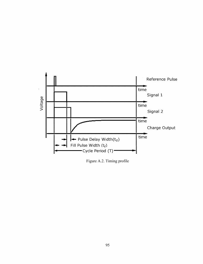
95
Figure A.2. Timing profile
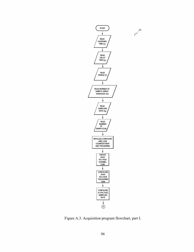
96
Figure A.3. Acquisition program flowchart, part I.

97
Figure A.4. Acquisition program flowchart, part II.

98
Figure A.5. Acquisition program flowchart, part III.

99
Figure A.6. Q-DLTS filtering flowchart, part I.

100
Figure A.7. Q-DLTS filtering flowchart, part II.

101
Figure A.8. Q-DLTS filtering flowchart, part III.

Figure A.9. Characteristic I
102
haracteristic I-V curve of the unstressed GaN/SiC blue LEDV curve of the unstressed GaN/SiC blue LED

Figure A.10. Q-DLTS spectra of
Figure A.11. Q-DLTS spectra of GaN/SiC blue LED, leakage compensated. Inset: Arrhenius plot..
103
DLTS spectra of GaN/SiC blue LED, non-compensated for leakage.
DLTS spectra of GaN/SiC blue LED, leakage compensated. Inset:
compensated for leakage.
DLTS spectra of GaN/SiC blue LED, leakage compensated. Inset:

104
GRANT STATEMENT
[0001] This invention was made with Government support under Grant No. NRC-
38-08-959 awarded by the Nuclear Regulatory Commission, Grant No. DE-FG07-
07ID14892 awarded by the Department of Education, and Grant No. W911SR-07-C-
0004 awarded by the Defense Threat Reduction Agency. The Government has certain
rights in the invention.
FIELD OF INVENTION
[0002] The present invention relates to a Deep Level Transient Spectrometer,
more specifically, to a Charge-based Deep Level Transient Spectrometer that is a
combination of a relatively simplified circuit structure and software-based signal
processing algorithms to achieve quantitative spectrum analysis.
BACKGROUND OF INVENTION
[0003] One of the most widely utilized methods for characterization of the deep-
level centers in semiconductors is Deep-Level Transient Spectroscopy or DLTS, first
proposed by D.V. Lang [2]. This technique is based on the measurement of junction
capacitance transients due to thermal emission during a return to equilibrium conditions;
however, conventional DLTS suffers from inherent setbacks. For example, if the series
resistance of the Device Under Test (DUT) is large, the capacitance transient may vary
with the measurement frequency. If the resistivity is large enough, the capacitance
transient might approximate the geometric capacitance for all measurement frequencies
[51]. For heavily doped materials, capacitance spectroscopy suffers from poor

105
sensitivity[52]. Furthermore, systems using a capacitance bridge for measurement are
inherently slow, which limits its usable range to traps above an activation energy of 0.1
eV [53]. Improvements have been made in the U.S. Patent No. 5,521,839 to Doolittle, et
al., which described a DLTS system that employs a pseudo-logarithmic data storage
scheme to digitize and analyze capacitance transients acquired from a test material [49].
[0004] Alternative measurement schemes have been proposed over the years.
These methods rely on the direct measurement of thermally stimulated current transients
[22], or the integration of these currents to yield charge transients (Q-DLTS) [6, 23, 24].
Most of these systems rely on hardware-based timing mechanisms to perform the
required DLTS signal processing. Computer systems that perform such functions have
been proposed but they are generally cumbersome or difficult to build [49].
[0005] Therefore, there is a need to provide a new, improved and straightforward
charge-based deep-level transient spectroscopy system with simplified circuit structure
and software-based signal processing algorithms to achieve quantitative spectrum
analysis in a timely fashion.
SUMMARY OF INVENTION
[0006] The invention provides a new and improved Charge-based Deep Level
Transient Spectrometer (Q-DLTS) with simplified circuit structure and software-based
signal processing algorithms. The inventive system comprises a detection means for
detecting charge transients of a semiconductor sample emitted under non-equilibrium
conditions, a modified ultra-fast switching circuit, an amplifier circuit, a modified
integration circuit based on said solid-state electronics, a data acquisition means for

106
digitizing the charge transients and in electronic communication with said detection
means, switching circuit, amplifier circuit, and integration circuit, and a software-based
controlling means in electronic communication with said data acquisition means, whereas
said controlling means further comprises a data analysis software for filtering and
smoothing the digitized charge transients and constructing a Q-DLTS spectrum of the
digitized charge transients.
DESCRIPTION OF DRAWINGS
[0007] Fig. 1 is an exemplary overall diagram for the inventive spectroscopy
system.
[0008] Fig. 2 is a timing waveform diagram showing the three counter/timer
signals and a characteristic exponential charge output during a single measuring cycle.
The top three waveforms are the voltage signals that control the switching, and Q0 is the
integrator output. On the abscissa, tf is the width of the forward bias pulse, td is the
signal delay width, and T is the period of a single measurement cycle.
[0009] Figs. A.3 to A.5 are the exemplary flowcharts of the sampling and timing
algorithm (process-command software).
[0010] Figs. A.6 to A.8 are the flowcharts of the Q-DLTS data analysis program.
[0011] Fig. A.9 is a graft illustrating I-V characteristics in a semi-logarithmic
scale of the as-received commercial GaN/SiC blue LED structure showing a typical diode
behavior.
[0012] Fig. A.10 is an uncompensated spectrum showing typical artifacts caused
by leakage currents and parasitic capacitance.

107
[0013] Fig. A.11 is a compensated Q-DLTS spectra obtained from the as-received
sample using ∆VB = 3.5 V, VB = –1.0 V, tc = 20 ms, td = 0 µs, T = 200 ms, NI = 100, and fs
= 250 kHz. Inset shows the Arrhenius trap dependence indicating an activation energy Ea
= 0.381 eV, and capture cross-section σ = 1.69E-17 cm2.
DETAILED DESCRIPTION OF INVENTION
[0014] Unless otherwise defined, all technical and scientific terms used herein
have the same meaning as commonly understood by one of ordinary skill in the art to
which this invention belongs. All publications, patent applications, patents, and other
references mentioned herein are incorporated by reference in their entirety.
[0015] The invention provides a new and improved Charge-based Deep Level
Transient Spectrometer (Q-DLTS) with a simplified circuit system and software-based
signal analysis algorithm to characterize the surface and bulk deep states in
semiconductor materials. The inventive system comprises i) a detection means for
detecting charge transients of a sample, ii) a modified switching circuit, iii) an amplifier
circuit, iv) a modified integration circuit, v) a data acquisition means for digitizing the
charge transients and regulating said detection means, switching circuit, amplifier circuit,
and integration circuit, and vi) a controlling means for controlling and integrating the data
detection, acquisition, and analysis process, whereas said controlling means is in
electronic communication with said data acquisition means and further comprises a data
analysis software for analyzing the digitized charge transients. The inventive system
provides the desired modularity capabilities, high sensitivity and simplicity of
construction.

108
[0016] Theory: The inventive Q-DLTS is developed upon the existing DLTS and
Q-DLTS techniques. As in Lang’s original dual-gated signal averaging or DLTS method,
the Q-DLTS technique relies on cyclic bias pulses to momentarily excite the traps of p-n
junctions and Schottky barriers. The electron occupation of a level is monitored as it
returns to thermal equilibrium by measuring the associated charge transients. In this
scheme, a “rate window” is defined as a function of two measuring gate times (t1 and t2)
starting at the beginning of the trap discharge. The charge transient is measured at these
two times and the difference, Q(t2)–Q(t1), is plotted as a function of temperature.
According to Maxwell-Boltzmann statistics, the thermal emission rates are strongly
dependent upon temperature. At a particular temperature, a thermal scan will produce an
emission rate that matches the rate window. Therefore, a peak in the spectrum is
produced because Q(t2)–Q(t1) is maximized. If several emission rates are present, then
multiple peaks appear.
[0017] If the time (t) dependent trap distribution is assumed to be uniform then
the current can be described as7
T
TT
tAqWN
ti
2
exp
)(
(1)
where A is the junction area, q is the elementary charge, W is the junction depletion
width, NT is the trap density, and τT is the decay time constant. To obtain the charge
emitted, the previous equation must be integrated over time,
T
Tt
o TT
Tt tAqWN
dttAqWN
dttitQ
exp12
exp20
(2)
The prefactor in Eq. (2) is the total charge collected,

109
20
0TAqWN
dttiQ
(3)
Traditionally in typical DLTS, the rate window or τ–1 is kept constant while the
temperature is varied. A similar method is to maintain a constant temperature while the
rate window is varied [6]. This rate window can be described as a function of the ratio of
the gate times (i.e., t2/t1=α) as
112
121
1
ln/ln
ttt
tt
(4)
Similar to Lang’s algorithm, the gate timed charge difference emitted from the beginning
of discharge is simply,
21 tQtQQ (5)
For electrons, the previous equation can be also written as,
210 expexp teteQQ nn (6)
where en is the electron emission rate, which has the form10
kT
ETe a
nn exp2 (7)
where σ is the capture cross-section, T is the temperature, Ea is the activation energy, k is
the Boltzmann constant, and Γn is defined as,
nn mkh 22/32/232 (8)
in which h is Planck’s constant and mn is the effective mass of the electron. The equations
for holes are analogous. For a given temperature, a maximum in the spectrum will occur
when the rate window equals the emission rate of the trap. This can be easily verified by
differentiating Eq. (6), which yields,

110
11
ln
ten
(9)
Substituting for α = 2 into Eq. (9) (which corresponds to the present embodiment) we
have,
1/2ln ten (10)
Substituting this value back into Eq. (6) we obtain,
4/0max QQ (11)
Eq. (11) is significant because it allows a direct calculation of the total charge collected
from the Q-DLTS peak maxima. Finally, because of the Arrhenius dependence of the
emission rate, the values of σ and Ea can be calculated using Eq. (7). Although not
described herein, further averaging algorithms such as nth Order Filtering [39], Fourier-
based Multi-Exponential DLTS [59] and the Gardner transform [60] are possible, and
even desired.
[0018] Circuit design: Refer to Fig. A.1, which is an exemplary overall diagram
for the hardware portion of the inventive system. As shown in Fig. A.1, the detection
means 1 may be a sensor or a semiconductor as Device Under Test (DUT), which is
placed in a temperature-controlled chamber 2. The detection means 1 along with the
switching circuit 3, the amplifier 4, and the integration circuit 5 are regulated by the data
acquisition means 6. According to the circuit design, only a low-noise integration
amplifier circuit (an LMC6001 ultra-low current amplifier from National Semiconductor
may be utilized) is required with fast switching capabilities. The high-speed Data
Acquisition (DAQ) Module 6 is further controlled by the controlling means 7 (such as a
PC). The system may also include multiple counter/timers 8. Accurate control of the

111
switching timing is essential to minimize the sampling of spurious signals, and the loss of
relevant data. The dual-gated signal averaging or other data processing schemes, and the
compensation for non-ideal circuit behavior are performed post-sampling by the
software. High SNRs can be obtained by multiple averaging and low-pass filtering of the
digitized data. This does not translate into longer processing times because the time
spent by traditional DLTS hardware circuits in repetitive measurement cycles of
increasing length is entirely avoided. Instead, the software algorithm speedily obtains the
desired emission spectrum.
[0019] Also shown in Fig. A.1, the input bias current of the device can be
compensated with a simple voltage divider circuit 9. For proper circuit behavior, leakage
currents must be controlled; especially at low input currents. Shield and guard rings can
be utilized to reduce leakage; however, it is better to have none of the terminals
associated with the pre-amplified input signal in contact with the printed circuit board
(PCB). Using air wiring and enclosing the whole circuit in a shielded enclosure
minimizes leakage, electrostatic interference and airborne ions impinging on the
integrating capacitors 10 [29]. If care is taken with the hardware components and
correction algorithms are employed to overcome non-ideal circuit behavior (i.e., charge
injection, parasitic capacitive coupling, electronic noise, etc.) then the sensitivity range of
the system can be extended into the femto-coulomb (fC) region. The maximum gain of
the present embodiment is Av,max ≈ 274 dB, thus a charge input of Qin = 100 fC would
yield a voltage output Vout = 0.5 V. The high sensitivity capabilities of the system are
evident in the low ΔQ values of the spectra shown in Figs A.9 and A.10.

112
[0020] The switching mechanism has proved to be the most challenging part of
the circuit design. It needs to be fast enough that the fast thermal emptying transients can
be sampled without signal degradation. At the same time, fast transients associated with
the switching charge injection need to be minimized. Several experiments with reed
relays were unsuccessful due to the large commutation noise and slow operating times.
Solid state analog switches based on CMOS technologies with sub-picoamp leakage
current and low charge injection (e.g., MAX326 from MaximTM) have proved to be more
successful . This type of device has also been utilized as the integrator reset switch that
controls the sampling/integration cycle.
[0021] The low-noise amplifier of the second gain-stage, 4, provides additional
gain. The LM741 op-amp may be utilized for this purpose with a built-in offset nulling
capability. This feature can be utilized to zero-out the output during the integrator reset
stage and null any jump caused by the switching charge injection [29].
[0022] Furthermore, the DUT, 1, filling voltage (∆VB) is provided by a voltage
divider, 11,shown in Fig. A.1 at the front end of the circuit diagram. This Parallel Mode
configuration is designed to probe the surface states of semiconductor-based sensors with
symmetrical electrodes deposited on the sensing surface [53]. However, if the DUT 1 is
a p-n or a Schottky diode then a reverse bias voltage is required during the relaxation part
of the measurement cycle. In Series Mode, switch 12 is kept open, and ∆VB is generated
from one of the DAQ analog outputs 14. This analog waveform can be externally
triggered by the Reference Signal (REF in Fig. A.2), and offset by the reverse bias or
quiescent voltage (VB) during the relaxation part of the measurement cycle.

113
[0023] Referring to Fig. A.2, the analog bias pulse width (tc) is configured to have
the same length as the delayed switching signal (i.e., tc = tf +td). As in Lang’s DLTS
method, two types of momentary filling or bias pulses are possible: a saturating injection
or forward bias pulse, which injects minority carriers into the depletion region, and a
majority carrier or reverse bias pulse, which introduces majority carriers into the
depletion region.
[0024] Timing Signals: Three counters/timers are needed to produce the timing
signals. The Reference Signal controls the period of the excitation/discharge cycle. The
period T needs be long enough for all the long-lived trapped charge transients to decay
away, which may be done by visually checking—with an oscilloscope 15 or a recurrent
voltage vs. time plot—for a flattening or plateauing of the total charge collected, and
ensuring that the next cycle starts at some point in this region.
[0025] In the present embodiment the Reference Pulse is obtained via a
counter/timer 8 (i.e., USB-4301 from Measurement ComputingTM [34]). This device is
based on the 9513 counter/timer chip, which has five independent 16-bit counters (i.e.,
65,536 maximum counts). All the counters are dependent on a single configurable
internal clock generator; thus, they cannot be used to output time events that are orders of
magnitude different. For example, the reference signal period can be as long as a few
seconds but the forward bias pulse width (tf) is often in the microsecond range. For this
reason, another separate counter/timer chip is required. Incidentally, the DAQ module 6
(USB-6221 from National Instruments™ [46]) used for the data acquisition has two 32-
bit independent counters that can be utilized for this purpose. These were used to
generate the Undelayed and Delayed Switching Signals using the Reference Pulse as a

114
trigger source. The adjustable delay (td) seen in the Delayed Signal is added to avoid the
integration of the aforementioned switching transients. This delay value must be chosen
carefully because the associated error (φ) is a function of the fastest charge transient
present in the DUT (τT).
[0026] The value of td must be chosen carefully because its associated error (φd) is
a function of the fastest charge transient present in the DUT (τT). Experiments with
several resistor/capacitor (RC) networks of various time constants yields the following
error formula,
971.0762.0exp1 Tdd t (12)
Experimentally, without a priori knowledge of τT, a delay of 3.0 µs was usually effective
to cancel out both the switching transients and parasitic coupling effects, while causing a
delay error of less than 5.0% for traps emission rates of time constants slower than 50 µs.
[0027] Analog to Digital (A/D) Conversion: The analog-to-digital (A/D)
conversion and timing program 20 is illustrated in the flowcharts shown in Figs. A.3 to
A.5.
[0028] The analog input (AI) task is set up by first creating an analog input
channel to measure voltage. Then, the user-defined sampling rate is configured by
setting the source of the sample clock. Finally, the triggering for the task is configured
using the delayed switching signal (SIG 2) as the trigger source. The start, read, and stop
parameters of the task are located inside a loop. Similar steps are performed for the
analog output (AO) task. Each filling pulse is associated with a particular transient decay
curve that is averaged after each cycle. The resulting data is stored in an array that is
carried from one iteration to the next via shift registers. The Signal-to-Noise Ratio

115
(SNR) can be significantly improved by increasing the number of iterations (NI). After
the preset number of iterations is reached, the averaged data array is saved in the PC
memory and a plot is generated.
[0029] The software communicates with the DAQ card via a single Universal
Serial Bus (USB) port. This data transfer protocol was chosen so the system would
maintain its portability by allowing the use of a laptop PC. Traditionally however,
external buses such as USB have suffered from poor latency and low bandwidth. To
ensure high-speed bidirectional analog data transfer over USB, the chosen DAQ device
features several advanced technologies. The data acquisition is hardware-timed and
buffered; that is, the data is transferred from the DAQ’s 12-bit First In/First Out (FIFO)
buffer to a data buffer in the PC memory. The DAQ device has two dedicated
Input/Output (I/O) onboard Data Memory Access (DMA) channels—among six that are
incorporated into the card’s Advanced Timing Controller. DMA data transfers free the
computer processor’s resources to execute other data operations. USB latency is greatly
improved with NI Signal Streaming technology. During the initial data request, the host
computer sends a single high-level message that is interpreted and converted by the DAQ
device processor itself, into the appropriate register-level commands to configure the
system and timing controller.
[0030] Q-DLTS Algorithm: The program illustrated in Figs. A.6 to A.8
essentially executes the algorithm described in the theory section. The first notable
addition is the calculation of the points on the abscissa or τ-axis; which, following the
convention in the literature, has units of log(μs). The parameter input sequence is inside

116
a loop structure to ensure that the sample rate constraints are met. If this is not achieved,
the program prompts the user to reenter all or some of these values.
[0031] The sampling rate of the de-excitation transient must be fast enough so
even the fastest thermal emissions can be processed by the Q-DLTS algorithm 31. This
can only be accomplished if the sampling rate (fs) 34, and the rate window initial (τ0) and
final (τf) values 32 obey two constraint equations. The first equation 35 is,
001 log^10log^10ln If s (13)
where I is the logarithmic rate window interval defined by
n
I f loglog 0 (14)
and n is the desired number of points on the abscissa of the Q-DLTS spectrum. It is easy
to verify that the subtraction terms in Eq. 13 correspond to τ1 and τ0, respectively.
Because the software is dealing with discrete values, the inverse of the sampling rate
cannot be lesser than the difference of the first two user selected values of t1.
[0032] Refer to Figs. A.6 to A.8, which illustrate the exemplary flowcharts for the
data acquisition process. For simplicity, the right side of Eq. 13 is called D 33. The
second constraint equation 36 is
N
f fs
ln1 (15)
where N is the total number of sampled points 33. The numerator of Eq. 15 corresponds
to the largest value of t2, thus the equation forces this value not to exceed the last sampled
data point. Since extrapolation is unfeasible in these ranges, the highest rate window and
its associated t2 value are the main reason for unused data. For simplicity, the right side

117
of Eq. 15 is called E 34. In the present embodiment, the maximum sampling rate fs,max=
250 kHz; therefore, the values of τ0, τf and n must be chosen accordingly.
[0033] The amplitude or charge output array is first smoothed by the mean
displaced ratio (MDR) method [65] and then digitally filtered via a Butterworth low-pass
filter 37. This filter was chosen due to its small frequency response characteristics;
however, other types of filters are possible. Knowing I, n and τ0 allows the program to
calculate each pair of t1 and t2 values by linear interpolation from the time array 40. The
corresponding charge values are then linearly interpolated from the amplitude array 41,
which was previously converted to units of charge (pC). Finally, the spectrum is plotted
and the data is stored in the PC’s memory. The Q-DLTS peaks are calculated by
grouping sequential data points in arrays of equal user-defined length. Each group of
data points are fit into quadratic polynomials and then differentiated twice to obtain each
peak’s amplitude, location and sharpness.
[0034] Compensation Methods for Non-Ideal Behavior: A typical Q-DLTS
uncompensated spectrum will show the presence of several non-ideal spectral features.
Most notably, the junction’s temperature-dependent leakage current under reverse bias is
unavoidably integrated alongside the charge output of the DUT, and appears as an
exponentially increasing charge at the tail end of the spectrum. This behavior can be
partially hardware-compensated with a bias resistor as shown in Fig.A.1; in addition, two
software leakage suppression methods are possible. If the leakage is integrated and
digitized from the diode under reverse bias, then this data set can then be subtracted to
the total charge output. An alternative algorithm is to calculate the slope of the curve of
the leakage vs. time after all transients attributed to carrier emission have decayed away

118
38. Since the leakage is constant, the slope is then used to artificially create an integrated
leakage current array that is subtracted from the total charge output array 39.
[0035] Another non-ideal spectral feature accentuated at low trap concentrations
are peaks associated with coupled parasitic capacitance (i.e., from coaxial cabling,
circuitry, etc.) and charge injection. These usually appear as fast time-independent
narrow peaks. For a given peak, the Q-DLTS spectrum yields information of both the
total charge output (Eq. 11) and the transient time constant (Eq. 9). These parameters can
be used to artificially generate the corresponding charge data array and subtract it from
the total DUT charge output. Another option is to use the delay time feature following
Eq.12; however, this option is only valid for capacitive coupling whenever its time
constant is faster than the fastest trap emission time constant.
[0036] EXAMPLE
[0037] Study of the acceptor levels present in commercial low brightness
GaN/SiC blue LED structures: Kingbright type KP-1608MBC blue LEDs were used.
Group-III nitrides LEDs have been extensively studied in the past in terms of failure
modes, degradation and aging mechanisms.[67-69]The photoluminescence in the blue
spectral range is obtained by the incorporation of Mg acceptor impurities, which results
in p-type doping. Nitrogen vacancies (VN) are also formed during the GaN growth with
similar concentrations of that of the Mg acceptor. The LED structures were of the form of
square dices (0.0136 × 0.0136 mm2) mounted p-side up on ceramic stems and
encapsulated in epoxy resin. For the present study, four LED junctions were placed in
parallel to increase the deep centers’ charge output [68]. Q-DLTS measurements were
carried out using the following parameter settings: ∆VB = 3.5 V, VB = –1.0 V, tc = 20 ms,

119
td = 0 µs, T= 200 ms, NI =100, Av = 226 dB, and fs = 250 kHz. This particular saturating
injection pulse voltage, which matches the GaN bandgap, was chosen to reveal the
minority-carrier traps (i.e., donor levels) present in the structure. The temperature range
is from 256 – 296 K measured in increments of ~7 K.
[0038] The characteristic I-V curve of the unstressed sample at room temperature
(Fig. A.9) confirms the presence of a p-n junction. Fig. A.10 shows the uncompensated
Q-DLTS spectrum of the as-received LED device. The graph shows the presence of a
typical isothermal capacitance peak at τ ≈50 μs; however, its small amplitude does not
interfere with the measurement of the main peak under test. Leakage effects, on the other
hand, are significant, and must be compensated for the peak-finding algorithm to function
properly. Fig. A.11 shows the compensated spectrum.
[0039] The filling pulse is long enough to assure that a quasisteady state and full
trap charge saturation are reached. This procedure is performed during the setup stage
and at low temperatures by increasing tc until no further long-lived peaks appear in the
spectrum. In samples with strong leakage currents, however, any long-lived peaks will
be buried by the integration process regardless of the correction algorithm employed. As
expected, the position of the visible single dominant peak shifts to shorter time constants
as the temperature is increased. From the Q-DLTS spectra, an Arrhenius plots was used
(inset of Fig.11) to calculate the values of the trap apparent activation energy Ea = 0.381
eV, and capture cross-section σ = 1.69E-17 cm2. These values closely match those found
in the literature for similar LED structures [67-69]. In particular, a state of similar
activation energy has previously been associated to a deep Mg-VN donor center. This
complex is formed when a Mg acceptor associates with an oppositely charged nearest-

120
neighbor nitrogen vacancy at high Mg doping levels. This complex, together with a Mg
shallow acceptor, participate in a donor-acceptor pair (DAP) transition that has been
shown to be responsible for the well-documented 2.8 eV blue photoluminescence band at
room temperature.
[0040] While the invention has been described in connection with specific
embodiments thereof, it will be understood that the inventive device is capable of further
modifications. This patent application is intended to cover any variations, uses, or
adaptations of the invention following, in general, the principles of the invention and
including such departures from the present disclosure as come within known or
customary practice within the art to which the invention pertains and as may be applied to
the essential features herein before set forth.
CLAIMS
What claimed is
1. A device for detecting surface and bulk deep states in semiconductor materials
comprising
i) a detection means for detecting charge transients of a sample or a device under ,
ii) a modified switching circuit,
iii) an amplifier circuit,
iv) a modified integration circuit,
v) a data acquisition means for acquiring and digitizing the charge transients, whereas
said data digitizing means is in electronic communication with said detection means,
switching circuit, amplifier circuit and integration circuit and

121
vi) a controlling means in electronic communication with said data acquisition means for
controlling the detection, acquisition, and digitization of the charge transients and
analyzing the digitized data.
2. The device of Claim 1, wherein said controlling means further comprising
i) a process-command software for regulating the detection, acquisition, and digitization
of the charge transients, and
ii) a data analysis software for analyzing the digitized charge transients and obtaining a
Q-DLTS spectrum based on Lang’s Dual-gated signal averaging or other filtering
method.
3. The device of Claim 1, wherein said detection means may be a sensor or a
semiconductor devise under test (DUT).
4. The device of Claim 1, wherein said data acquisition means may be a smart data
acquisition module with ultra-high data throughput capabilities.

122
BIBLIOGRAPHY
[1] Ippommatsu, M., et al., Sensing Mechanism of SnO2 Gas Sensors. J. Mater. Sci., 1990. 25: pp. 259-262.
[2] Lang, D. V., Deep-level transient spectroscopy: A new method to characterize traps in semiconductors J. Appl. Phys., 1974. 45: p. 3023.
[3] LabVIEW ( Laboratory Virtual Instrumentation Engineering Workbench) is a platform and development environment from National Instruments Corporation, 11500 N Mopac Expwy., Austin, TX 78759-3504.
[4] Smith, M. R., et al., Decomposition of Multicomponent Exponential Decays by Spectral Analytic Techniques. Technometrics, 1976. 18(467-482).
[5] Rothenberger, J. B., Construction of a Test Chamber for Ultra-Low Gas Concentrations and Its Use for Testing Novel Aluminum Nitride Sensors by Q-DLTS, in Nuclear Science and Engineering Institute. 2011, University of Missouri: Columbia.
[6] Arora, B. M., et al., Deep-level transient charge spectroscopy of Sn donors in AlxGa1-xAs. J. Appl. Phys., 1993. 73(4): pp. 1802-1806.
[7] Balland, J. C., et al., Investigation of deep levels in high-resistivity bulk materials by photo-induced current transient spectroscopy: II. Evaluation of various signal processing methods. J. Phys. D: Appl. Phys., 1986. 19: pp. 71-87.
[8] Sque, S. J., et al., Structure, electronics, and interaction of hydrogen and oxygen on diamond surfaces. Phys. Rev. B, 2006. 73(085313): pp. 1-15.
[9] Loh, K. P., et al., Surface Oxygenation Studies on (1 0 0)-Oriented Diamond Using an Atom Beam Source and Local Anodic Oxidation. Surface Science, 2002. 505: pp. 93-114.
[10] Maier, F., et al., Origin of surface conductivity in diamond. Phys. Rev. Lett., 2000. 85(16): pp. 3472-3475.
[11] Helwig, A., et al., On the Low-Temperature Response of Semiconductor Gas Sensors. J. Sens., 2009. 2009: pp. 1-17.
[12] Helwig, A., et al., Gas sensing properties of hydrogen-terminated diamond.Sensors and Actuators B, 2008. 133: pp. 156-165.
[13] Ristein, J., et al., The Role of Adsorbates and Defects on Diamond Surfaces. New Diamond and Frontier Carbon Technology, 2000. 10(6): pp. 363-382.
[14] Robertson, J. and Rutter, M. J., Band Diagram of Diamond and Diamond-like Carbon Surfaces. Diam. Rel. Mater., 1998. 7: pp. 620-625.

123
[15] Koslowski, B., et al., Comment on "Origin of Surface Conductivity in Diamond".Phys. Rev. Lett., 2001. 87(20): pp. 209705-209701.
[16] Szameitat, M., et al., Influence of Adsorbates on the Surface Conductivity of Chemical Vapor Deposition Diamond. Appl. Phys. Lett., 2000. 77(10): pp. 1554-1556.
[17] Liu, F. B., et al., Electronic Properties of Hydrogen- and Oxygen-Terminated Diamond Surfaces Exposed to Air. Chinese Phys. B, 2009. 18(5): pp. 2041-2047.
[18] Lang, D. V., Recalling the origins of DLTS. Physica B, 2007. 401-402: pp. 7-9.
[19] Mahmood, Z. H., et al., Charge Deep Level Transient Spectroscopy of Electron Traps in MOVPE Grown n-GaN on Sapphire. Physica Status Solidi b, 2008. 245(11): pp. 2567-2571.
[20] Tokuda, Y., et al., Deep-level transient spectroscopy using low-frequency capacitance measurements in XIII International Conference on Semiconducting and Insulating Materials. 2004: Beijing, China. p. 222-225.
[21] Borsuk, J. A. and Swanson, R. M., Current Transient Spectroscopy: A High-Sensitivity DLTS System. IEEE Trans. Electron Devices, 1980. 27(12): pp. 2217 -2225.
[22] Wessels, B. W., Determination of deep levels in Cu-doped GaP using transient-current spectroscopy J. Appl. Phys., 1976. 47(3): pp. 1131-1133.
[23] Kirov, K. I. and Radev, K. B., A Simple Charge-Based DLTS Technique. Phys. Status Solidi A, 1981. 63: pp. 711-716.
[24] Farmer, J. W., et al., Charge transient spectroscopy Appl. Phys. Lett., 1982. 41: pp. 1063-1065.
[25] Clayton, G. B., Operational Amplifiers. 1979, Boston: Newnes-Butterworths.
[26] Polyakov, V. I., et al., Effects of post-growth treatment and coating with ultrathin metal layers on the band bending and field electron emission of diamond films.Journal of Applied Physics, 1998. 84(5): pp. 2882-2889.
[27] National Semiconductor Corporation, Worldwide Headquarters, 2900 Semiconductor Drive, Santa Clara, California.
[28] LMC6001 Ultra Ultra-Low Input Current Amplifier, N.S. Corporation, Editor. 2009, National Semiconductor Corporation.
[29] Rako, P., Measuring Nanoamperes. EDN, 2007: p. 42.
[30] Texas Instruments Incorporated, 12500 TI Boulevard, Dallas, Texas 75243.
[31] MAX326 CMOS analog switch, available from Maxim Integrated Products Inc., 120 San Gabriel Drive, Sunnyvale, CA 94086.

124
[32] Seidel, D. L., Sample-and-Hold Switch with Low On Resistance and Reduced Charge Injection, U.S. Patent, Editor. 1992, NCR Corporation: US.
[33] WEB RED Catalog 2006 Rev. 5-5-08, in 9800 Series/Surface Mount Reed Relays. 2006, Coto Technology: USA.
[34] Measurement Computing Corporation, 10 Commerce Way, Norton, MA 02766.
[35] USB-4301 9513-Based Counter/Timer User's Guide. 2008, Measurement Computing Corporation.
[36] InstaCal is distributed free of charge by Measurement Computing Corporation, 10 Commerce Way, Norton, MA 02766.
[37] Thurzo, I. and Grendel, M., On the Relationship Between the Feedback Charge Method, Charge Transient Spectroscopy and C-V Measurements of Semiconductors and Insulators. Meas. Sci. Tech., 1992. 3: pp. 726-731.
[38] Thurzo, I. and Gmucova, K., Switching Between Deep-Level Transient Spectroscopy and Feedback Charge Capacitance Modes in a Versatile Time-Domain Spectrometer. Rev. Sci. Instrum., 1993. 67(7): pp. 2244-2248.
[39] Crowell, C. R. and Alipanahi, S., Transient Distortion and nth Order Filtering in Deep Level Transient Spectroscopy (DnLTS). Solid-State Electronics, 1981. 24(1): pp. 25-36.
[40] Hanak, T. R., et al., A new method to analyze multiexponential transients for deep-level transient spectroscopy. J. Appl. Phys., 1990. 67(9): pp. 4126-4132.
[41] Henini, M., et al., A microcomputer-based deep level transient spectroscopy (DLTS) system. J. Phys. E, 1985. 18: pp. 926-929.
[42] Morimoto, J., et al., Multi-exponential analysis of DLTS. Applied Physics A: Materials Science & Processing, 1986. 39(3): pp. 197-202.
[43] Morimoto, J., et al., Spectral Analysis of Deep Level Transient Spectroscopy (SADLTS). Jpn. J. Appl. Phys., 1987. 26(10): pp. 1634-1640.
[44] Okuyama, M., et al., Fourier-transformation analysis of deep level transient signals in semiconductors. Solid-State Electronics, 1982. 26(7): pp. 689-694.
[45] Weiss, S. and Kassing, R., Deep Level Transient Fourier Spectroscopy (DLTFS)-A technique for the analysis of deep level properties. Solid-State Electron., 1988. 31(12): pp. 1733-1742.
[46] National Instruments Corporation, 11500 N Mopac Expwy, Austin, TX 78759-3504.
[47] InOmTech is a Registered Trademark of InterOmni Technologies LLC., 681 Mountain Rd, West Hardford, CT 06117.

125
[48] (2006) ASMEC-06 Automatic System of Material Electro-Physical CHaracterization Basic Unit User Manual.
[49] Doolittle, W. A. and Rohatgi, A., A novel computer based pseudo-logarithmic capacitance/conductance DLTS system specifically designed for transient analysis.Rev. Sci. Instrum., 1992. 63(12): pp. 5733-5742.
[50] Radioshack Corporation, Riverfront Campus World Headquarters, 300 RadioShack Circle, Fort Worth, TX 76102-1964.
[51] Mahmood, Z. H., et al., Charge deep level transient spectroscopy of electron traps in MOVPE grown n-GaN on sapphire. Phys. Status Solidi B, 2008. 245(11): pp. 2567-2571.
[52] Miller, G. L., et al., Capacitance Transient Spectroscopy. Annu. Rev. Mater. Sci., 1977. 7: pp. 377-448.
[53] Kachwalla, Z. and Miller, D. J., Transient spectroscopy using the Hall effect Appl. Phys. Lett., 1986. 50: pp. 1438-1440.
[54] Kirov, K. I. and Radev, K. B., A simple charge-based DLTS technique. Phys. Status Solidi A, 1981. 63(2): pp. 711-716.
[55] Arora, B. M., et al., Deep-level transient charge spectroscopy of Sn donors in AlxGa1−xAs. J. Appl. Phys., 1993. 73: pp. 1802-1807.
[56] Doolittle, W. A. and Rohatgi, A., A novel computer based pseudo-logarithmic capacitance/conductance DLTS system specifically designed for transient analysis.Rev. Sci. Instrum., 1992. 63: pp. 5733-5741.
[57] Polyakov, V. I., et al., Effects of post-growth treatment and coating with ultrathin metal layers on the band bending and field electron emission of diamond films J. Appl. Phys., 1998. 84: pp. 2882-2889.
[58] Crowell, C. R. and Alipanahi, S., Transient Distortion and nth Order Filtering in Deep Level Transient Spectroscopy (DnLTS). Solid-State Electron., 1981. 24: pp. 25-36.
[59] Morimoto, J., et al., Multi-Exponential Analysis of DLTS. Appl. Phys. A, 1986. 39: pp. 197-202.
[60] Gardner, D. G., et al., Method for the Analysis of Multi-Components Exponential Decays. J. Chem. Phys., 1959. 31(4): pp. 978-986.
[61] LM741 operational amplifier, available from National Semiconductor Corporation, 1152 Kifer Road, Sunnyvale, CA 94086.
[62] Tapiero, M., et al., Photoinduced current transient spectroscopy in high-resistivity bulk materials: Instrumentation and methodology. J. Appl. Phys., 1998. 64(8): pp. 4006-1012.

126
[63] The Technologies Powering NI M Series DAQ, available at: http://zone.ni.com/devzone/cda/tut/p/id/2849.
[64] NI Signal Streaming: Sustaining High-Speed Data Streams on External PC Buses, available at: http://zone.ni.com/devzone/cda/tut/p/id/4636.
[65] Dyson, R. D. and Isenberg, I., Analysis of exponential curves by a method of moments, with special attention to sedimentation equilibrium and fluorescence decay. Biochemistry, 1971. 10(17): pp. 3233-3241.
[66] KP-1608MBC blue LED, available from Kingbright Corporation, 225 Brea Canyon Road, City of Industry, CA 91789, USA.
[67] Meneghesso, G., et al., Failure Modes and Mechanisms of DC-Aged GaN LEDs.Phys. Status Solidi A, 2002. 194(2): pp. 389-392.
[68] Zdansky, K., et al., Degradation of commercial high-brightness GaP:N green light emitting diodes. J. Appl. Phys., 1998. 83(12): pp. 7678-7684.
[69] Arslan, E., et al., The persistent photoconductivity effect in AlGaN/GaN heterostructures grown on sapphire and SiC substrates. J. Appl. Phys., 2008. 103: p. 103701.
[70] Meneghesso, G., et al., Degradation mechanisms of GaN-based LEDs after accelerated DG current aging. IEDM 2002: pp. 103-106.
[71] Smith, M., et al., Mechanisms of band-edge emission in Mg-doped p-type GaN.Appl. Phys. Lett., 1996. 68(14): pp. 1883-1885.
[72] Kaufman, U., et al., Nature of the 2.8 eV photoluminescence bancd in Mg doped GaN. Appl. Phys. Lett., 1998. 72(11): pp. 1326-1328.
[73] Qu, B. Z., et al., Photoluminescence of Mg-doped GaN grown by metalorganic chemical vapor deposition. J. Vac. Sci. Technol. A, 2003. 21(4): pp. 838-841.
[74] Bestaev, M. V., et al., Study of the Surface Structure of Tin Dioxide Layers for Gas Sensors by Atomic-Force Microscopy. Semiconductors, 1998. 32(6): pp. 587-589.
[75] Polyakov, V. I., et al., Effect of Various Adsorbates on Electronic States of the Thin Diamond-Like Carbon Films. Diamond Relat. Mater., 2006. 15(11): pp. 1926-1929.
[76] Gi, R. S., et al., Possibility of realizing a gas sensor using surface conductive layer.Jpn. J. Appl. Phys., 1997. 36: pp. 2057-2060.
[77] Gaudin, O., et al., Deep level transient spectroscopy of CVD diamond: the observation of defect states in hydrogenated films. Diamond Relat. Mater., 2001. 10: pp. 610-614.
[78] Ristein, J., et al., Band diagrams of intrinsic and p-type diamond with hydrogenated surfaces. Phys. Status Solidi A, 2003. 199(1): pp. 64-70.

127
[79] Available from Element Six, 35 West 45th St., New York, NY 10036, USA.
[80] Monch, W., Adsorbate-induced suface states and Fermi-level pinning at semiconductor surfaces. J. Vac. Sci. Technol. B, 1989. 7(5): pp. 1216-1225.
[81] Looi, H. J., et al., High carrier mobility in polycristaline thin film diamond. Appl. Phys. Lett., 1998. 73(3): pp. 353-355.
[82] Denisenko, A., et al., Hypothesis on the conductivity mechanism in hydrogen terminated diamond films. Diamond Relat. Mater., 2000. 9: pp. 1138-1142.
[83] Wolkenstein, F. F., Electronic processes at the surface of semiconductor during chemisorption. Sov. Phys. Usp., 1967. 9(5): pp. 743-751.
[84] Nebel, C. E., et al., Electrochemical properties of undoped hydrogen terminated CVD diamond. Diamond Relat. Mater., 2006. 15: pp. 264-268.
[85] Deferme, W., et al., Electrical transport measurements and emission properties of freestanding single crystalline CVD diamond samples. Phys. Status Solidi A, 2007. 9: pp. 3017-3022.
[86] Ristein, J., et al., Surface doping: a special feature of diamond. J. Phys.: Condens. Matter, 2001. 13: pp. 8979-8987.
[87] Prelas, M. A., et al., Electrostatic Thin Film Chemical and Biological Sensor. US Patent No 20080007267A1, 2008.
[88] Blood, P. and Orton, J. W., The electrical characterization of semiconductors: majority carriers and electron states. Techniques in Physics, ed. N.H. March. Vol. 1. 1992, Oxford, England: Academic Press.
[89] Thurzo, I., et al., Experimental evidence for complementary spatial sensitivities of capacitance and charge deep-level transient spectroscopies. Semicond. Sci. Technol., 2000. 15: pp. 378-385.
[90] Tipton, A., An Exploration of Chemical Agents Detection Using the Quantum Fingerprint Technology, in Nuclear Science and Enginerring Institute. 2009, University of Missouri: Columbia.
[91] Tanimura, Y., et al., High-temperature operation of a radiation detector made of a type IIa diamond single crystal synthesized by a HP/HT method. Nuc. Instrum. Methods A, 2000. 443(325-330).
[92] Zheng, J. C., et al., Oxygen-induced surface state on diamond (100). Diam. Rel. Mater., 2001. 10: pp. 500-505.
[93] Gerbi, J. E., et al., Electrical contacts to ultrananocrystalline diamond. Appl. Phys. Lett., 2003. 83(10): pp. 2001-2003.

128
[94] Galbiati, A., et al., Performance of Monocrystalline Diamond Radiation Detectors Fabricated Using TiW, Cr/Au and a Novel Ohmic DLC/Pt/Au Electrical Contact.IEEE Trans. Nuc. Sci., 2009. 56: pp. 1863-1874.

129
VITA
Daniel E. Montenegro was born in Montevideo, Uruguay on September 11, 1974. He
attended Brigham Young University-Idaho in Rexburg, Idaho where he received an
Associate of Science degree in Electrical Engineering in April 2002. Later, he attended
Idaho State University in Pocatello, Idaho, where he received a Bachelor of Science
degree in Electrical Engineering in December 2004 and a Master of Science degree in
Nuclear Engineering in July 2009. He continued his education at the Nuclear Science of
Engineering Institute of the University of Missouri where he received a Doctor of
Philosophy degree in Nuclear Engineering in July 2011. He is married to Rebecca W.
Montenegro. During the preparation of this dissertation, his family was increased by the
birth of two daughters, Eva Grace and Maria Elizabeth.


![Fabrication of (111)-Faced Single-Crystal Diamond Plates ... · type-IIa, CVD single-crystal diamond from Element6 [43]. 2. The edge and face orientations of these samples are shown](https://img.pdfslide.us/doc/110x75/5f56855f8b04ce4bee2a1452/fabrication-of-111-faced-single-crystal-diamond-plates-type-iia-cvd-single-crystal.jpg)