Embed Size (px)
DESCRIPTION
Single point diamond turning
Citation preview
Investigation on Diamond Turning of Silicon Crystal -
Generation Mechanism of Surface Cut with Worn Tool
Renato G. Jasinevicius, Jaime G. Duduch, Arthur J. V. Porto, Universidade de São Paulo-
EESC, Department of Mechanical Engineering Caixa Postal 359, 13560-970. São Carlos, S.P.
Brazil, [email protected]
This paper discusses the effect of tool wear on surface finish in single-point diamond turning of
single crystal silicon. The morphology and topography of the machined surface clearly show the
type of cutting edge wear reproduced onto the cutting grooves. Scanning electron microscopy is
used in order to correlate the cutting edge damage and microtopography features observed
through atomic force microscopy. The possible wear mechanisms affecting tool performance and
surface generation during cutting are also discussed. The zero degree rake angle single point
diamond tool presented small nicks on the cutting edge. The negative rake angle tools presented
more a type of crater wear on the rake face. No wear was detected on flank face of the diamond
tools.
Keywords: Wear, diamond machining, silicon crystal, topography, scanning electron microscopy,
atomic force microscopy
Introduction
Brittle materials are used for their superior properties and ability to take a polish. In the machining
of normally brittle crystals, when extremely sharp tools are used, plastic behavior may take place
prior to the onset of fracture when the cut is restricted below critical cutting depth value (Puttick
and Franks, 1990, Duduch et al. 1996). In single point diamond turning, the surface roughness is
extremely low as a result of the high fidelity reproduction of the cutting edge profile. Because of
this, the cutting edge sharpness of diamond tools used in the machining of brittle materials is of
extreme relevance in achieving optical quality surface finish and low subsurface damage.
The feasibility of using this process as a finishing operation for optical components from
semiconductor crystals has increased significantly. The anomalous plasticity observed in diamond
turning of silicon at room temperature may be attributed to a phase transformation induced by
pressure/stress generated by the tool edge/tip contact (Morris et al. 1995). Evidences reported on
high pressure (Minomura and Drickamer, 1962, Jameison, 1963) and indentation (Gridneva et al.
1972, Clarke et al. 1988) experiments have demonstrated that diamond-cubic silicon transforms to
the denser metallic -tin structure under hydrostatic pressure at room temperature and; upon
release of the pressure, a reversion to another form, i.e., an amorphous semiconductor phase, with
a cubic structure has been reported (Hu et al.1986). The critical pressure observed to cause a
transformation to a metallic -tin structure is in the range of 11.3-12.5 GPa, under pure hydrostatic
conditions (Clarke et al. 1988). However, this is reduced to values as low as 8 GPa when shear
stresses are present (Gilman, 1992). Material removal will then be ductile, resultant from the
metallic thin layer which is plastically removed.
However, silicon crystal may impose some constrain in terms of changing cutting edge geometry.
This can be translated into rapid wear and cutting edge damage. The tool edge bluntness extent
can be considered a relevant aspect of influence in respect of the critical cutting dimensions in this
machining process. It is worth mentioning that for the brittle-to-ductile transition, the critical
thickness of cut and/or critical cutting depth, have been found to be in the range of 50-250 nm for
Si (Blake and Scattergood, 1990, Blackley and Scattergood, 1991) using commercially available
diamond tools with edge radii larger than 100 nm. Furthermore, a less sharp tool implies in higher
contact pressure and higher cutting forces and stresses in the tool’s active zone. When a blunt or
worn tool is used, the cutting depth required will be higher in order to generate sufficient amount
of stress to drive the phase transformation. Moreover, when larger depth of cut are used, worn
tools will probably tend to cause brittle failure before metallization occurance. The control and/or
attenuation of wear in diamond tools is a fundamental factor to improve the performance of
micromachining in terms of the applicability and economy of the process.
This paper presents an investigation on the surface generation mechanism involved in single-point
diamond turning of single crystal silicon with a worn tool. Possible wear mechanisms affecting
tool performance during cutting will be discussed. Scanning electron microscopy (SEM) analysis
of tool wear features are presented. The wear pattern of single point diamond tools used to machine
single crystal silicon and the effect of this wear on the surface generated are presented. Atomic
Force Microscopy (AFM) will be used to characterize the morphology and topography of the
machined the machined formed with a damaged tool.
Experimentals
Test Procedure, Experimental Apparatus and Geometry of the Diamond Turning Process
Single-point diamond turning tests were carried out on a commercially available ultraprecision
diamond turning machine, the Aspheric Surface Generator Rank Pneumo ASG 2500. Facing cuts
were performed on monocrystalline silicon samples (10 x 10 mm2). Single crystal p-type Si was
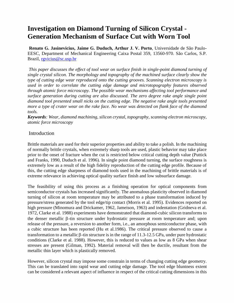
used in this study. Silicon having (100) surface orientation was used. Table I gives the properties
of single crystal silicon.
In this work, round nose single crystal diamond tools (Contour Fine Tooling®) were used. Only
new diamond tools were used in the cutting tests. The schematic diagram of the profile of the
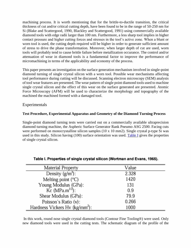
tool/material interaction where brittle-to-ductile transition occurs is depicted in Fig. 1. The chip
thickness (t) varies from zero at the tool center up to a maximum tmax at the top of the uncut
shoulder. There is a gradual decrease in the severity of the damage along the shoulder. The
transition from ductile mode to brittle mode is represented by the parameter yc , which is the critical
depth, and by the critical chip thickness tc. The position of the transition moves downward along
the tool nose as the feed rate increases. This cutting model was first proposed by Blake and
Scattergood (1990). The severity of microfracture damage will be higher close to the top of the
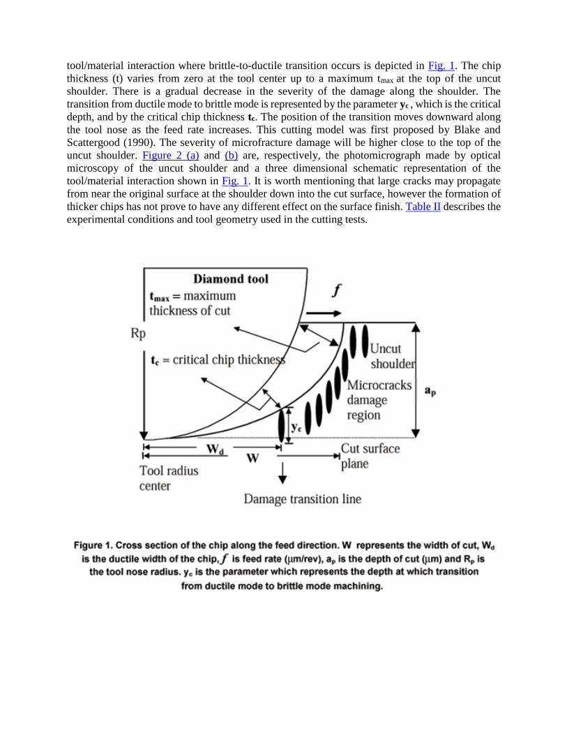
uncut shoulder. Figure 2 (a) and (b) are, respectively, the photomicrograph made by optical
microscopy of the uncut shoulder and a three dimensional schematic representation of the
tool/material interaction shown in Fig. 1. It is worth mentioning that large cracks may propagate
from near the original surface at the shoulder down into the cut surface, however the formation of
thicker chips has not prove to have any different effect on the surface finish. Table II describes the
experimental conditions and tool geometry used in the cutting tests.
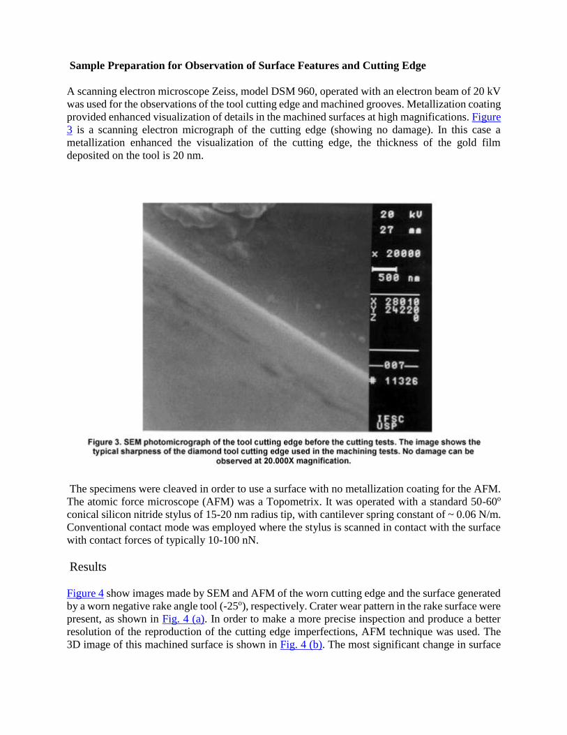
Sample Preparation for Observation of Surface Features and Cutting Edge
A scanning electron microscope Zeiss, model DSM 960, operated with an electron beam of 20 kV
was used for the observations of the tool cutting edge and machined grooves. Metallization coating
provided enhanced visualization of details in the machined surfaces at high magnifications. Figure
3 is a scanning electron micrograph of the cutting edge (showing no damage). In this case a
metallization enhanced the visualization of the cutting edge, the thickness of the gold film
deposited on the tool is 20 nm.
The specimens were cleaved in order to use a surface with no metallization coating for the AFM.
The atomic force microscope (AFM) was a Topometrix. It was operated with a standard 50-60o
conical silicon nitride stylus of 15-20 nm radius tip, with cantilever spring constant of ~ 0.06 N/m.
Conventional contact mode was employed where the stylus is scanned in contact with the surface
with contact forces of typically 10-100 nN.
Results
Figure 4 show images made by SEM and AFM of the worn cutting edge and the surface generated
by a worn negative rake angle tool (-25o), respectively. Crater wear pattern in the rake surface were
present, as shown in Fig. 4 (a). In order to make a more precise inspection and produce a better
resolution of the reproduction of the cutting edge imperfections, AFM technique was used. The
3D image of this machined surface is shown in Fig. 4 (b). The most significant change in surface
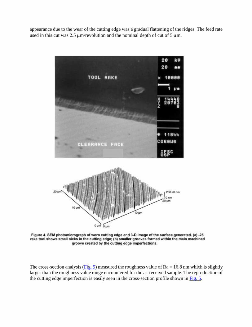
appearance due to the wear of the cutting edge was a gradual flattening of the ridges. The feed rate
used in this cut was 2.5 m/revolution and the nominal depth of cut of 5 m.
The cross-section analysis (Fig. 5) measured the roughness value of Ra = 16.8 nm which is slightly
larger than the roughness value range encountered for the as-received sample. The reproduction of
the cutting edge imperfection is easily seen in the cross-section profile shown in Fig. 5.
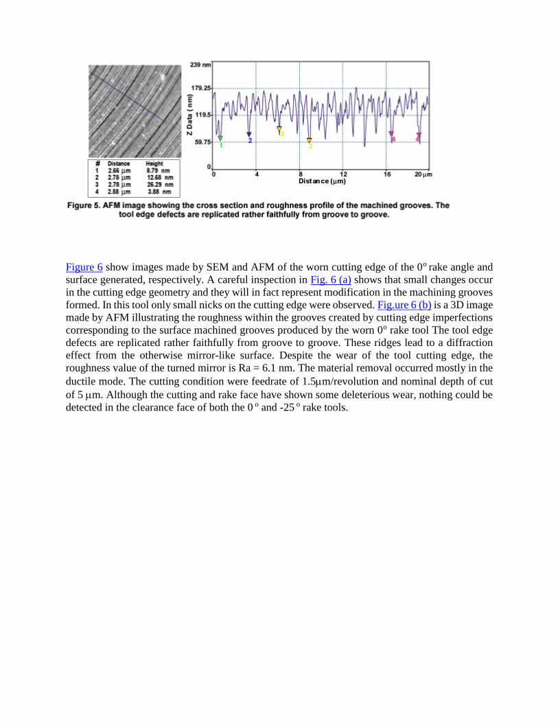
Figure 6 show images made by SEM and AFM of the worn cutting edge of the 0o rake angle and
surface generated, respectively. A careful inspection in Fig. 6 (a) shows that small changes occur
in the cutting edge geometry and they will in fact represent modification in the machining grooves
formed. In this tool only small nicks on the cutting edge were observed. Fig.ure 6 (b) is a 3D image
made by AFM illustrating the roughness within the grooves created by cutting edge imperfections
corresponding to the surface machined grooves produced by the worn 0o rake tool The tool edge
defects are replicated rather faithfully from groove to groove. These ridges lead to a diffraction
effect from the otherwise mirror-like surface. Despite the wear of the tool cutting edge, the
roughness value of the turned mirror is Ra = 6.1 nm. The material removal occurred mostly in the
ductile mode. The cutting condition were feedrate of 1.5m/revolution and nominal depth of cut
of 5 m. Although the cutting and rake face have shown some deleterious wear, nothing could be
detected in the clearance face of both the 0 o and -25 o rake tools.

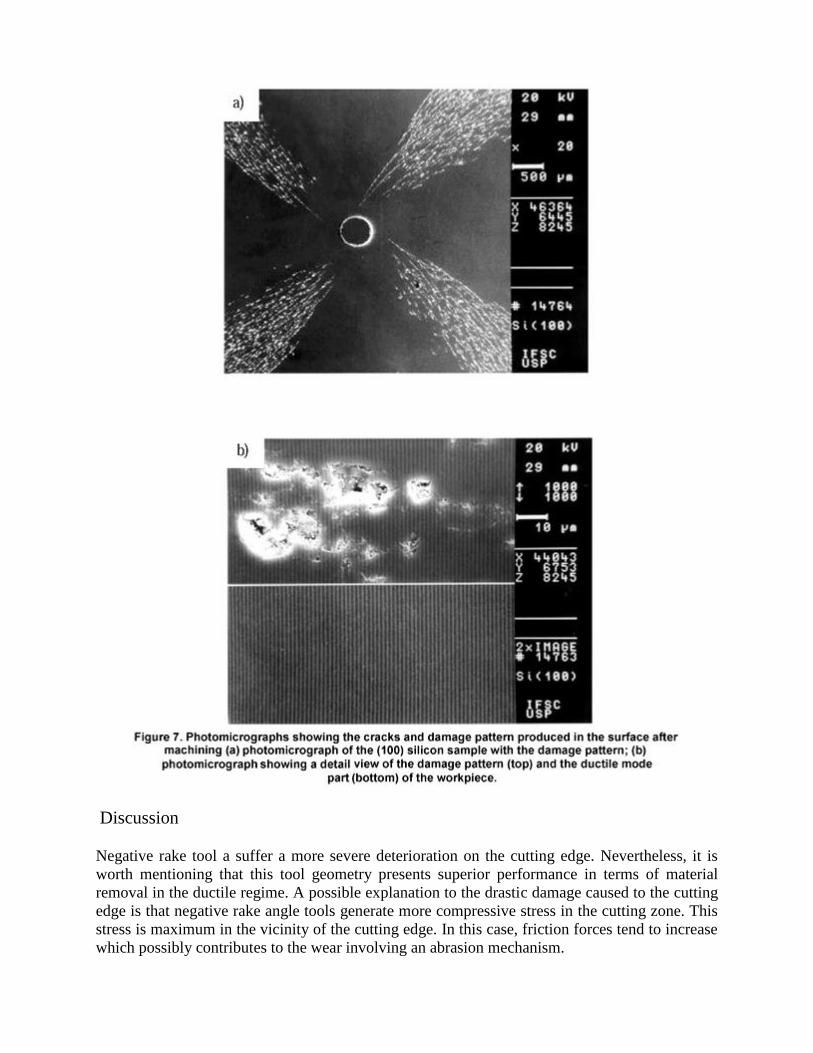
During machining with worn tool an interesting damage pattern was observed. Certain areas of the
sample had a ductile response and others brittle responses as shown in Fig. 7. Figure 7 (a) illustrates
the cracks and damage pattern formed. Figure 7 (b) show detailed view of both regimes, i.e., brittle
and ductile. The top image revealed cracks running perpendicular to the cutting direction. The
bottom image shows the surface finish in the ductile mode. The cutting condition were feedrate of
1.25 m/revolution and nominal depth of cut of 0.1 m using negative rake angle tool.
Discussion
Negative rake tool a suffer a more severe deterioration on the cutting edge. Nevertheless, it is
worth mentioning that this tool geometry presents superior performance in terms of material
removal in the ductile regime. A possible explanation to the drastic damage caused to the cutting
edge is that negative rake angle tools generate more compressive stress in the cutting zone. This
stress is maximum in the vicinity of the cutting edge. In this case, friction forces tend to increase
which possibly contributes to the wear involving an abrasion mechanism.
It is well established that silicon and germanium can be diamond machined, however silicon
presents a more aggressive edge wear (Blake and Scattergood, 1990) when compared with
germanium. The estimate of wear rates for the pair diamond/silicon is of great relevance for the
machining of this material under feasible production rates. Specific wear rates for diamond tips
and silicon were determined in sliding tests (Khurshudov et al. 1997) performed in Atomic Force
Microscope. The estimated values of the wear rate of diamond in contact with silicon were 1.4 x
10 -9 mm3 N-1 m-1 and 4.5 x 10⁻⁴ mm3 N-1 m-1, respectively.
The relationship between the material hardness and wear can be considered a factor of particular
relevance to the analysis of the performance of a single point diamond tool and the development
of wear (Hurt and Decker, 1984). The reported wear rate for diamond/silicon interaction is
comparable with the rate reported for the wear of diamond in contact with hard steel (Thornton
and Wilks, 1978) (2.0 x 10⁻⁹ mm3 N-1 m--1). The high wear rate with hard steel is due to the large
chemical affinity of the iron with the carbon of the diamond. Ferrous metals in contact with
diamond tools can rapidly wear the cutting edge. Diamond shows a considerable weight loss by
oxidation or graphitization when exposed to high temperatures (Davies and Evans, 1972). These
particular observations give support to the thermomechanical process which is an important
mechanism of wear of a diamond cutting edge. According to Hurt & Decker (1984), temperatures
during diamond machining can easily reach 427 oC (or 700 oK). This only causes a moderate
reduction in diamond strength (Brookes, 1979). During single point diamond turning of non-
ferrous metals the temperature on the cutting edge and rake face is not sufficiently high to
thermally reduce diamond strength. Furthermore, the maximum temperature found on the rake
face of a diamond tool was approximately 190 C for aluminum and 220 C for copper at cutting
speed of 620 m/min (Ueda et al. 1998). A successfully attempt has been made by Abdel-Aal et al.
(1997) to calculate the temperature development during the simulated machining of silicon and
germanium wafers. The results indicated that the workpiece surface temperature rise is well bellow
the thermal softening temperatures for these materials under the conditions applied in the tests.
Particularly the temperature rise was of about 80 oC for Ge and less than 400 oC for Si. These can
be considered of moderate magnitude and are proportional to the loads and speeds used in the tests
(idem).
The exact mechanism responsible for the wear of single point diamond tools used in the
micromachining of silicon has not yet been completely explained. Paul and collaborators (1996)
have not found any strong evidence of chemical wear caused by silicon/diamond tool interaction.
According to them, because silicon contains no d electrons, no chemical wear is predicted by
electron complex mechanism. Hence, processes that result in scratches or gouges are signs of non
chemical wear (idem). It is believed that hard particle may be formed during micromachining
process. Consequently, this is likely to promote the polishing of the cutting edge. Recently, it was
reported (Puttick et al. 1995) the detection of thin superficial film of oxide residues on the virgin
surface of as-received polished silicon wafers and nanoturned surfaces (0.5 nm and 1.5 nm thick
of SiO2, respectively). In the case of the nanoturned specimen a significant amount of carbon was
also found, possibly transferred from the diamond tool. Molecular dynamics simulation
techniques, applied to the understanding of the mechanisms involved in the nanomachining
process of silicon, have detected the presence of SiC particles as well as the graphitization of the
diamond tool cutting edge (Boercker et al. 1992). On the other hand, no evidence of the formation
of this abrasive material (SiC) was detected through XPS technique on single point diamond turned
monocrystalline silicon surfaces (Kunz et al. 1996). The presence of small particles formed by
silicon debris found in the tool edge/material interface can aid the promotion of abrasive wear of
diamond.
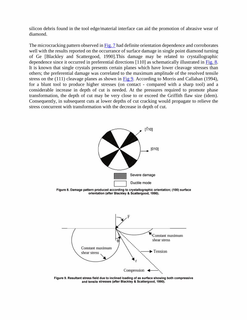
The microcracking pattern observed in Fig. 7 had definite orientation dependence and corroborates
well with the results reported on the occurrance of surface damage in single point diamond turning
of Ge [Blackley and Scattergood, 1990].This damage may be related to crystallographic
dependence since it occurred in preferential directions [110] as schematically illustrated in Fig. 8.
It is known that single crystals presents certain planes which have lower cleavage stresses than
others; the preferential damage was correlated to the maximum amplitude of the resolved tensile
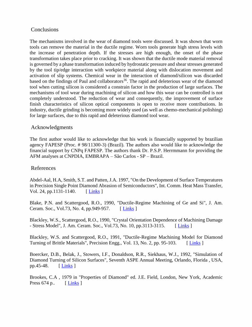
stress on the (111) cleavage planes as shown in Fig 9. According to Morris and Callahan (1994),
for a blunt tool to produce higher stresses (on contact - compared with a sharp tool) and a
considerable increase in depth of cut is needed. At the pressures required to promote phase
transformation, the depth of cut may be very close to or exceed the Griffith flaw size (idem).
Consequently, in subsequent cuts at lower depths of cut cracking would propagate to relieve the
stress concurrent with transformation with the decrease in depth of cut.
Conclusions
The mechanisms involved in the wear of diamond tools were discussed. It was shown that worn
tools can remove the material in the ductile regime. Worn tools generate high stress levels with
the increase of penetration depth. If the stresses are high enough, the onset of the phase
transformation takes place prior to cracking. It was shown that the ductile mode material removal
is governed by a phase transformation induced by hydrostatic pressure and shear stresses generated
by the tool tip/edge interaction with workpiece material along with dislocation movement and
activation of slip systems. Chemical wear in the interaction of diamond/silicon was discarded
based on the findings of Paul and collaborators36. The rapid and deleterious wear of the diamond
tool when cutting silicon is considered a constrain factor in the production of large surfaces. The
mechanisms of tool wear during machining of silicon and how this wear can be controlled is not
completely understood. The reduction of wear and consequently, the improvement of surface
finish characteristics of silicon optical components is open to receive more contributions. In
industry, ductile grinding is becoming more widely used (as well as chemo-mechanical polishing)
for large surfaces, due to this rapid and deleterious diamond tool wear.
Acknowledgments
The first author would like to acknowledge that his work is financially supported by brazilian
agency FAPESP (Proc. # 98/11300-3) (Brazil). The authors also would like to acknowledge the
financial support by CNPq FAPESP. The authors thank Dr. P.S.P. Herrmmann for providing the
AFM analyses at CNPDIA, EMBRAPA – São Carlos - SP – Brazil.
References
Abdel-Aal, H.A, Smith, S.T. and Patten, J.A. 1997, "On the Development of Surface Temperatures
in Precision Single Point Diamond Abrasion of Semiconductors", Int. Comm. Heat Mass Transfer,
Vol. 24, pp.1131-1140. [ Links ]
Blake, P.N. and Scattergood, R.O., 1990, "Ductile-Regime Machining of Ge and Si", J. Am.
Ceram. Soc., Vol.73, No. 4, pp.949-957. [ Links ]
Blackley, W.S., Scattergood, R.O., 1990, "Crystal Orientation Dependence of Machining Damage
- Stress Model", J. Am. Ceram. Soc., Vol.73, No. 10, pp.3113-3115. [ Links ]
Blackley, W.S. and Scattergood, R.O., 1991, "Ductile-Regime Machining Model for Diamond
Turning of Brittle Materials", Precision Engg., Vol. 13, No. 2, pp. 95-103. [ Links ]
Boercker, D.B., Belak, J., Stowers, I.F., Donaldson, R.R., Siekhaus, W.J., 1992, "Simulation of
Diamond Turning of Silicon Surfaces", Seventh ASPE Annual Meeting, Orlando, Florida , USA,
pp.45-48. [ Links ]
Brookes, C.A , 1979 in "Properties of Diamond" ed. J.E. Field, London, New York, Academic
Press 674 p.. [ Links ]
Clarke, D.R., Kroll, M.C., Kirchner, Cook, R.F. and Hockey, 1988, "Amorphization and
Conductivity of Si and Ge During Indentation", Phys. Rev. Lett., Vol. 60, No. 21, pp.2156-
2159. [ Links ]
Crompton, D., Hirst, W., Howse, M.G.W., 1973 "The Wear of Diamond". Proc. Royal Soc.
(London). Vol. A.333, pp.435-454. [ Links ]
Davies, G. and Evans, T., 1972, "Graphitization of Diamond at Zero Pressure and at High
Pressure", Proc. R. Soc. (London), Vol. A. 328, pp.413-427. [ Links ]
Duduch, J.G., Gee, A E., Porto, A J. V., Jasincevicius, R.G., Carpinetti, L.C.R., 1996 "Model of
Brittle Materials Single Point Machining with Removal Rates". Revista Brasileira de Ciências
Mecânicas (Journal of the Brazilian Society of Mechanical Sciences), Vol. 18, No. 1, pp.33-
39. [ Links ]
Gerk, A. P., Tabor, D., 1978 "Indentation Hardness and Semiconductor-Metal Transition of
Germanium and Silicon", NATURE, Vol.271, p.732-733. [ Links ]
Gilman, J.J., 1992, "Insulator-Metal Transitions at Microindentations", J. Mater. Res. Vol. 7, No.
3, pp.535-538. [ Links ]
Gridneva, I.V., Milman, Y.V., Trefilov, M., 1972 "Phase Transformation in Diamond-Structure
Crystals During Hardness Measurements", Phys. Status Solidi A, Vol. 14, pp. 177-
182. [ Links ]
Hiatt, G.D. and Strenkowski, J.S., 1991, "Fracture Mechanics Applied to the Ductile Machining
of Brittle Materials", Proc. 7th ASPE Annual Meeting, Greenleaf, FLA, USA, pp.29-
32. [ Links ]
Hu, J.Z., Markle, L.D., Menoni, C.S., Spain, I. L., 1986, "Crystal Data for High-Pressure Phases
of Silicon", Phys. Rev. B., Vol. 34, No. 7, pp. 4679-4684. [ Links ]
Hurt,H.H., Decker, D.L., 1984 "Tribological Considerations of the Diamond Single Point Tool",
Proc. of the SPIE, Production aspects of single point machined optics, Vol. 508, pp.126-
131. [ Links ]
Jameison, J.C., 1963, "Crystal Structures at High Pressures of Metallic Modifications of Si and
Ge", Science, Vol.139, pp.762-764. [ Links ]
Jasinevicius, R.G., Duduch, J.G., Porto, A J.V. 1998 "Two Fracture Modes Observed Through
SEM in Brittle-to-Ductile Regime Diamond Turning Of Monocrystalline Silicon", ACTA
MICROSCOPICA, Vol. 7 (Suppl. A), pp. 417-420. [ Links ]
Kunz, R.R., Clark, H.R., Nitishin, P.M., Rothschild, M., Ahern, B.S., 1996 "High Resolution
Studies of Crystalline Damage Induced by Lapping and Single-Point Diamond Machining of
Si(100)", J. of Mater. Res., Vol. 11, No. 5, pp.1228-1237. [ Links ]
Khurshudov, A.G., Kato, K., Koide, H., 1997, "Wear of the AFM Diamond Tip Sliding Against
Silicon", WEAR, Vol.203-204, pp.22-27. [ Links ]
Minomura, S., Drickamer, H.G., 1962 "Pressure-Induced Phase Transformations in Si, Ge, and
Some III-V Compounds", J. Phys. Chem. Solids, Vol. 23, pp.451-456. [ Links ]
Morris, J.C., Callaham, D.L., 1994 "Origins of the Ductile Regime in Low Load Scratching in Si",
J. Mater. Res.,Vol.9, No. 11, pp.2907-2913. [ Links ]
Morris, J.C., Callaham, D.L.,Kulik, J., Patten, J. A. and Scattergood, R.O., 1995, "Origins of the
Ductile Regime in Single Point Diamond Turning of Semiconductors", J. Am. Ceram. Soc., Vol.
78, No. 8, pp.2015-2020. [ Links ]
Nakasuji, T., Kodera, S., Hara, S., Matsunaga, H., Ikawa, N. and Shimada, S., 1990, "Diamond
Turning of Brittle Materials for Optical Components", Annals of the CIRP, Vol.39, No. 1, pp.89-
92. [ Links ]
Paul, E., Evans, C.J., Manganmelli, A, McGlauflin, M. L., Polvani, R. S., 1996 "Chemical Aspects
of Tool Wear in Single Point Diamond Turning", Precision Engg., Vol. 18, pp.4-19. [ Links ]
Pizani, P. S., Jasinevicius, R.G., Duduch, J.G. and Porto, A J.V. 1999, "Ductile and Brittle Damage
in Single Point Diamond Turned Silicon Probed by Raman Scattering", Journal of Materials
Science Letters, Vol. 18, pp. 1185-1187. [ Links ]
Puttick, K.E., Franks, A., 1990, "The Physics of Ductile-Brittle Machining Transitions: Single
Point Theory and Experiment", Jap. Soc. Prec. Engg., Vol. 56 , No. 5, pp.12-16. [ Links ]
Puttick, K.E., Whitmore, L. C., Gee, A.E., Chao, C.L., 1995 "Energy Scaling Transitions in
Machining of Silicon by Diamond". Trybology International, Vol. 28, No. 6, pp.349-
355. [ Links ]
Suzuki, T., Ohmura, T, 1996, "Ultramicroindentation of Silicon at Elevated Temperatures", Phil.
Mag. A, Vol. 74, No. 5, pp.1073-1084. [ Links ]
Thornton, A.G., Wilks, J., 1978, "Clean Surface Reactions Between Diamond and Steel". Nature,
Vol.274, No. 24, pp.792-793. [ Links ]
Ueda, K., Sugita, T, Hiraga, H., 1991 "A J-Integral Approch to Material Removal Mechanism in
Microcutting of Ceramics", Annals of the CIRP, Vol. 40, No. 1, pp.61-64. [ Links ]
Wortman, J.J. and Evans, R.A, 1965, "Young’s Modulus, Shear Modulus, and Poissons’s Ratio in
Silicon and Germanium", J. Appl. Phys., Vol. 36, No. 1, pp.153-156. [ Links ]
Ueda, T., Sato, M. and Nakayama, K., 1998, "The Temperature of a Single Crystal Diamond Tool
in Turning" Annals of the CIRP, Vol. 47 , No. 1, pp.41-44. [ Links ]