Embed Size (px)
Citation preview

M. Angelone, D. Lattanzi, M. Pillon, M. Marinelli, E. Milani, A. Tucciarone,G. Verona-Rinati, S. Popovichev, R.M. Montereali, M.A. Vincenti, A.Murari
and JET EFDA contributors
EFDA–JET–PR(07)56
Development of Single CrystalDiamond Neutron Detectors
and Test on the JET Tokamak

“This document is intended for publication in the open literature. It is made available on theunderstanding that it may not be further circulated and extracts or references may not be publishedprior to publication of the original when applicable, or without the consent of the Publications Officer,EFDA, Culham Science Centre, Abingdon, Oxon, OX14 3DB, UK.”
“Enquiries about Copyright and reproduction should be addressed to the Publications Officer, EFDA,Culham Science Centre, Abingdon, Oxon, OX14 3DB, UK.”

Development of Single CrystalDiamond Neutron Detectorsand Test on the JET Tokamak
1Associazione EURATOM-ENEA sulla Fusione, C.R. Frascati, C.P. 65, I-00044 Frascati (Roma) Italy2Associazione EURATOM -Università di Roma “Tor Vergata”, Dipartimento di Ingegneria Meccanica,
Via del Politecnico 1, I-00133 Roma, Italy3EURATOM-UKAEA Fusion Association, Culham Science Centre, OX14 3DB, Abingdon, OXON, UK
4ENEA, Physical Technologies and New Materials Dep., C.R. Frascati, C.P. 65, I-00044 Frascati (Roma) Italy5Consorzio RFX - Associazione EURATOM-ENEA sulla Fusione, Corso Stati Uniti 4, 35127 Padova, Italy
* See annex of M.L. Watkins et al, “Overview of JET Results ”, (Proc. 21 st IAEA Fusion Energy Conference, Chengdu, China (2006)).
Preprint of Paper to be submitted for publication inNuclear Instruments and Methods in Physics Research Section A
JET-EFDA, Culham Science Centre, OX14 3DB, Abingdon, UK

.

1
ABSTRACT.
During the 2005-2007 JET experimental campaigns a Single Crystal Diamond detector (SCD)
covered with a 2µm thick LiF film 95% enriched in 6Li, was installed at JET and operated
continuously during the whole experimental campaign with the goal to measure both the total and
the time dependent neutron emission from plasmas. After reviewing the history of diamond as
neutron detector for tokamak application, this paper reports on the experimental measurements
performed during that time window. The obtained results are compared with those obtained with
detectors routinely working at JET (fission chambers and silicon diodes). In particular it was
demonstrated that using a SCD detector covered with a 6LiF film it has been possible to discriminate
between the total and the 14MeV neutrons coming from triton burn-up. This allowed, for the first
time using a single detector, the contemporary measurement of the total and 14MeV neutron yields
as well as their time dependency with very good reliability and stability.
1. INTRODUCTION
The fusion community is presently involved in the construction of the International Tokamak
Experimental Reactor (ITER) [1]. This project is supported by seven partners (EU, USA, RF, Japan,
China, South Korea and India) and the tokamak is going to be built in France (at Cadarache). The
ITER project is very challenging and many are the scientific and technological problems to be
faced and solved. Among them, the detection of neutrons emitted from ITER plasmas represents a
challenge due to the expected large neutron and gamma fluence. Some of the presently used
techniques, for example at JET (e.g. silicon and scintillators detectors), cannot be used or will
suffer serious radiation damage problems. Another problem to be considered for the proper
functioning of the detector is the working temperature which in ITER is well above the ambient
temperature. The development of neutron and radiation sensors capable to withstand ITER working
conditions is one of the key issues of fusion neutronic activities. Since many years several attempts
were made to use both natural and artificial diamond as detecting medium. In principle, all kind of
radiation (from charge particles to UV and neutrons) are detectable by diamond. Many application
have been proposed and tested, they span from fundamental and high energy physics to dosimetry,
from UV and X and gamma-rays to neutrons. Just as an example see [2, 3, 4, 5].
The choice of diamond as detecting material is related to the many outstanding properties of this
material [6], such as radiation hardness [7], low sensitivity to gamma rays, fast response and high
energy resolution. Due to these particular properties and its very fast response it is considered as
one of most promising detecting materials [8] despite the many problems encountered in its
production, among them the difficulty to produce films with standard and reproducible properties.
This problem is intrinsically due to the used CVD technique which is based upon plasma deposition.
The future of CVD diamonds is the production of electronic grade single crystals which up to now
has been reported by a few groups [9, 10, 11, 12]. A single crystal has 100% collection efficiency,
energy resolution comparable to that of silicon detectors (values up to 0.3% were reported [13]), no

2
polarization effects and do not need priming, i.e. irradiation with electromagnetic or beta radiation
prior to the use so as to passivate internal traps.
In the field of neutron detectors ENEA C.R. Frascati and Rome “Tor Vergata” University are
cooperating since many years to develop electronic grade artificial diamond films grown by Chemical
Vapour Deposition (CVD) and to be used as neutron detectors in ITER. A systematic study of the
diamond properties and behaviour is being conducted.
The development of CVD diamond detectors by our group started with the production of
polycrystalline films at the end of the 1990’s and after several attempts led to the production of
monocrystalline films which promise to fulfil the requests for ITER neutron detectors. Since many
fundamental improvements of diamond films have so far been obtained, it is perhaps time to briefly
review the story of diamond neutron detectors pursued by our group in order to set the achieved
points and to discuss what needs to be further investigated. In the next section the development of
CVD diamond neutron detectors is shortly reviewed before discussing their construction (sect. 3)
and the result of their test at JET tokamak during the 2005-2007 experimental campaigns (Sect.4).
Foreseen developments are also highlighted in section 4.
2. A SHORT STORY OF CVD DIAMOND NEUTRON DETECTORS
The development of nuclear detectors based upon artificial diamond films started about ten years
ago with the first radiation detectors produced with the goal to study the physical properties of the
CVD films. The basic idea was to use charged particles as probes. Since efficient particle detectors
require high drift lengths of the carriers produced by the ionizing radiation, the presence of defects
severely limits the performances of the device. From the study of the response of artificial diamond
detectors irradiated with charged particles (alphas and betas) it is thus possible to get information
about the different kind of defects formed inside the film and affecting the detector response. The
analysis of the response of CVD diamond-based detectors was used to extract both qualitative and
quantitative information on the properties of the various defects limiting the free movement of
electrons and holes carriers produced by the radiation in the detector (e.g. type of defects, activation
energy, geometrical distribution etc.). In the early days of our work only very simple sandwiched
detectors were realized made of CVD polycrystalline film with gold or aluminium contacts deposited
by evaporation processes. Despite the simplicity of the system many and fundamental improvements
were obtained by studying the response of these devices when irradiated with 5.5MeV alphas
produced by 241Am source and/or betas from 90Sr. The results concerning these studies are reported
in [14] and references therein. Here it is stressed the importance that the study of the priming
procedure and the identification of defects had on the development and improvement of
polycrystalline CVD detectors performances.
Owing to the well known (n, α) reactions of carbon with fast neutrons that led in the past to use
natural diamonds as fast neutron detectors [2], it was almost natural to extend the study of these
devices to irradiation with 14MeV neutrons produced by the 14MeV Frascati Neutron Generator

3
(FNG) [15]. The first positive test with 14MeV neutrons dates on fall 2002. A 500µm thick
polycrystalline film sandwiched with gold contacts of 2 mm diameter was irradiated at FNG for
about 15000 sec showing good stability and negligible polarization effects [16].
The first successful application of a polycrystalline CVD diamond as 14MeV neutron detector
in a tokamak dates on November 2003 during the JET Trace Tritium Experiment (TTE) and
represents a milestone for artificial diamond films studies [17]. In this first attempt 14MeV neutrons
emitted from JET operating with DT plasmas were detected. Total and time dependent 14MeV
neutron emission during each shot were measured with the diamond detector and the results
correlated very well with the same data recorded by the conventional silicon diodes. Since this
date many relevant improvements were obtained, among them the production of Single Crystal
Diamond (SCD) with excellent spectrometric performance (energy resolution lower than 1%)
and good stability [18] which did not require the priming procedure to work properly.
A further step was represented by the fabrication of diamond layered detectors with a boron
doped conductive layer [19] grown on the substrate (Fig.1) prior to intrinsic diamond layer (active
region) deposition. The layered SCD detectors proved to be both well reproducible in the detector
performances (e.g. resolution within 1-2% for all the produced samples) and unaffected by
polarization effects as well. This layered structure enabled to realize diamond detectors without
the need to remove the growing substrate that usually is made of a commercial low grade HTHP
single crystal diamond and which is not suitable as a detector medium. The substrate removal
procedure is expensive and dangerous since there is the possibility to break or damage the high
quality diamond film.
Last, but not least, the production of layered SCD detectors covered with Lithium Fluoride (LiF)
films 95% enriched in 6Li was achieved soon after [19]. The latter detectors, through the 6Li(n, α)T
reaction in 6Li and the direct detection of α, T and fast neutrons in the diamond bulk, allow for
contemporary detection of thermal and 14MeV neutrons [19]. It was also demonstrated that these
detectors can withstand high neutron fluxes [20], up to 2E+9 ncm-2 sec-1. Work is in progress to
demonstrate that this detector can be used as an active tritium production monitor as well.
To conclude this short review about diamond neutron detectors, it ought to be mentioned that
SCD films are also applied for X-ray and UV detection [21] and this seems to be very promising
for ITER.
The continuous improvement of the diamond film quality and thus of the detector performances
has been possible tanks to their test at JET under very challenging tokamak working conditions.
In the recent 2005-2007 experimental campaigns two artificial diamonds detectors both covered
with 6LiF films were installed at JET. The first detector was of polycrystalline type with traditional
sandwiched structure while the second was a SCD diamond with layered structure. Both detectors
operated continuously during the whole experimental campaigns. Since polycrystalline films are
no longer of interest to us as neutron detectors and, also, accounting for the fact that results obtained
with detectors based on them were already published [22], this paper reports about the results
4
obtained for the Single Crystal Diamond (SCD) detector during the whole JET experimental 2005-
2007 campaigns and addresses some future work.
3. EXPERIMENTAL
3.1 DETECTOR FABRICATION
A layered SCD detector was grown on top of a commercial high pressure high temperature HPHT
Ib single crystal diamond used as growing substrate. The substrate was 3mm × 4mm in surface and
about 400µm thick. The layered detector was produced by means of a two steps CVD homoepitaxial
process. In the first step a boron-doped (conducting) diamond buffer layer of about 15µm thickness
and resistivity of about 5Ω is deposited on top of the HPHT substrate. In the second step, performed
in a separated CVD reactor to avoid unwanted boron contamination, an intrinsic diamond film
deposition is performed. This deposition thickness is in the range 5-200µm depending upon the
detector’s use. In our case, since the main goal was to test the performances of new layered detectors,
the bulk of the intrinsic deposit was 35µm. The backing contact was thus realized by using the B-
doped layer while on the growing surface a 2.5mm diameter and 100nm thick Al contact was
thermally evaporated. This multilayered structure (Fig.1) allows separating the response of the
high quality intrinsic bulk diamond from that originated inside the thick HPHT diamond substrate,
if any. The electrical signal to be processed arises only inside the high quality CVD layer avoiding
the need for mechanical removal of the HPHT substrate. Usually at this stage a test of the film
quality is performed by a multi-peaks alpha source (241Am+240Pu+244Cm) whose energy ranges in
between 5.5 and 5.8MeV. This test allows verifying: a) stability during long lasting irradiations to
check whether or not the detectors are affected by polarization effects; b) charge collection efficiency,
c) the energy resolution (Fig.2).
Up to now this test was very positive since all the grown layered detectors (almost one hundred)
shown high time stability, 100% efficiency and resolution lower than 2% regardless of detector
thickness. The best detector, with an intrinsic CVD layer of 100µm, showed a resolution as low as
0.5%. The above data demonstrate that production of CVD films with homogeneous response is no
longer a dream.
Last, but not least, a 2µm thick 6LiF film was directly grown on top of the Al contact by thermal
evaporation [23] at ambient temperature and at vacuum pressure lower than 5×10⁻⁶ mbar. The
deposition was performed at the Solid State Lasers Laboratory of ENEA C.R. Frascati. 6LiF tablets
(3mm × 3mm × 0.9mm) enriched to 95.62% in 6Li were used as starting material for the deposit.
The tablets were heated at about 800oC in a tantalum crucible placed below the CVD substrate. The
sample was clamped on a rotating holder. The evaporation rate was fixed to a value of 1nm/s and
controlled by an INFICON quartz oscillator. The thickness of the 6LiF film was also directly measured
by means of a Tencor P10 profilometer on 6LiF films grown on a glass and silicon substrates during
the same evaporation run. After production, the SCD detector was tested again with 5.5MeV alpha
particles from 241Am source in order to check its stability and collection efficiency.

5
The 6LiF layer deposited on top of the SCD detector acts as converting medium by taking advantage
of the well known 6Li + n → 3H + 4He nuclear reaction, which converts slow energy neutrons into
two charge particles (3H with energy of 2.73MeV and 4He with energy of 2.06MeV, respectively)
which are emitted in opposite directions and directly absorbed into the high purity diamond layer
producing two peaks which are clearly resolved by the detector. At the same time diamond is
sensitive to high energy neutrons which produce the (n, α) reactions in Carbon [2]. In particular the
so called (n, α) reaction with a threshold at about 5.7MeV produces a well isolated peak which is
easily resolved by the detector. The performances of the detector can be easily described by looking
at Fig.3, where a typical Pulse Height Spectrum (PHS) recorded at FNG by means of MCA is
reported. The detector was inside a 5cm thick polyethylene phantom in order to slow down some of
the 14MeV neutrons produced by FNG and to enhance the interaction with 6Li. The spectrometric
performances are clearly pointed out by the wide separation among the various peaks.
It is important to point out that, due to the adopted layered structure, only (n, α) reactions produced
inside the high quality SCD film are recorded in the spectrum while those produced, if any, in the
HTHP substrate are grounded by the boron layer. The SCD detector with 6LiF layer thus allows for
the contemporary detection of slow energy and 14MeV neutrons. In the following it will be labelled
LiDia detector (Lithium Diamond detector).
The contemporary detection of slow energy and 14MeV neutrons is particularly relevant to
fusion neutronics since in DD and/or DT plasmas both 2.5MeV and 14MeV neutrons are produced.
Presently they are measured with different detectors (e.g. fission chambers and silicon diodes).
It ought to be stressed that when operating with DD plasmas the 14MeV neutrons are only
produced by the triton burn-up i.e. the tritons slowing-down in the plasma before reacting with
Deuterium. The 14MeV neutron emission is then delayed by about 300-400ms with respect to the
2.5MeV neutrons produced by DD reaction. This delay time is the typical slow down time of tritons
born with about 1MeV energy in the JET tokamak. Furthermore, the intensity of the delayed neutron
emission is about 1% of that due to DD neutrons. For a detector to work properly one must expect
it to be able to separate the two components also from a temporal point of view.
3.2 DETECTOR INSTALLATION AT JET
The LiDia detector was installed at JET in June 2006 inside the Torus Hall near the main vertical
port in Octant 1, at about 4m apart from the plasma centre. Its data acquisition began from JET
Pulse No: 66654. The detector worked with a bias of +3 V/µm for the whole duration of the JET
experimental campaigns, which ended in April 2007.
The LiDia detector was directly connected to a charge preamplifier ORTEC Mod. 142A and
both detector and preamplifier were located inside a metallic box (Fig.4). The connection to shaping
amplifier and threshold discriminators, located outside the torus hall in the diagnostic area, was
obtained by means of long 50Ω coaxial cables (about 100m). The shaping amplifier was working
with shaping time of 1µsec. The logic signals produced by the discriminators were acquired in

6
terms of count rate versus time by the JET acquisition system CODAS. Two discrimination thresholds
were set. The lowest (THR-1) was able to detect all the signals produced by the neutrons regardless
of their energy (total neutron yield), the second threshold (THR-2) was set well above the first one
in order to detect only the signals due to 14 MeV neutrons and produced by the (n, α) reaction. To
set this threshold the standard three-peaks alpha source was used to calibrate the voltage output
signal versus radiation energy.
4. RESULTS AND DISCUSSION
Since the LiDia detector was not absolutely calibrated, the results reported in the following are
compared with respect to the standard detectors in use at JET, that are the 235U fission chambers
(KN1 diagnostic) for total neutron emission and silicon diodes (KM7 diagnostic) for 14MeV neutron
emission. Both integral and time dependent emission data will be considered.
It ought to be stressed that during the whole experimental campaign JET operated with DD plasmas
so the 14MeV emission was due to triton burn-up, that is about 1% of the total neutron emission. This,
together with the low reaction cross section (about 70mb) and the very small detector volume is the
reason for the poor counting statistics obtained for 14MeV neutrons with the SCD detector.
In Fig.5 the correlation between LiDia detector and the KN1 diagnostic versus the total neutron
yield is reported. Data refer to more than 800 JET pulses and cover the whole 2005-2007 experimental
campaigns during which some high current and high neutron yields pulses were produced. As can
be seen from Fig.5 the correlation is very strong both at the lowest and highest neutron yields.
In Fig.6 the ratio between LiDia and KN1 counts is plotted versus the JET pulse number, e.g. as
function of time. Again an excellent stability is observed and most of the data lie within one standard
deviation which is lower than -3%. A further proof of the capability of the LiDia detector to properly
operate in a tokamak is given in Fig.7, where the distribution function (histogram) of the above
mentioned ratio is plotted. It is fitted by a Gaussian function demonstrating that the observed
variations are due to counting statistics.
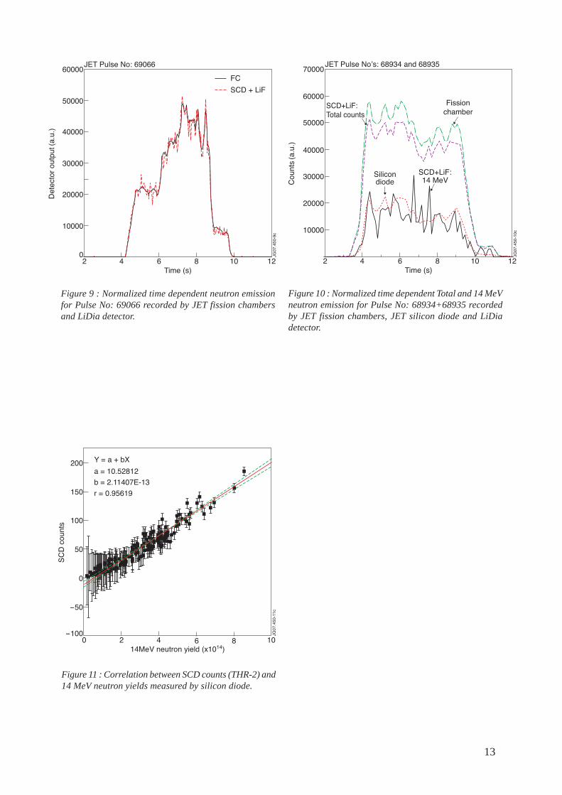
Figures 8 and 9 report just an example of how the LiDia detector can reproduce the time dependent
total neutron emission by comparison with KN1 data. The reported figures point out that even
sudden variation in the neutron production are perfectly reproduced by the SCD detector (Fig.9). It
ought to be stressed that this comparison was made for all JET pulses over the whole experimental
campaign and the results again confirmed the capability of the SCD diamond detector to properly
work. When considering Fig.9 another point to be considered is that fission chambers at JET work
in current mode while our detector operates in pulse mode. Furthermore, while the fission chambers
are embedded in a thick polyethylene shield to slow down neutrons, our detector was naked so
there was an huge difference in the counting efficiency. Despite this the results are very good.
The most important feature of the LiDia detector is the already mentioned capability to contemporary
detect total and 14MeV neutron emission. This is proven by Fig.10, where both neutron emissions
as recorded by LiDia, KN1 (for the total emission) and Silicon diode (for 14MeV neutrons emission)

7
are compared for Pulse No’s: 68934 and 68935. The sum of at least two pulses is necessary for
14MeV neutrons only due to the low counting statistics. It ought to be stressed that since JET
operated in DD and the volume of the SCD was very small the comparison is meaningful only for the
highest neutron yields. Despite this limitation the analysis clearly points out that the time dependent
14MeV neutron emission is well reproduced by the LiDia detector. Also the time delay due to triton
slow down is well reproduced as it is evidenced by comparing with silicon diode output.
Last, but not least, also the total 14 MeV neutron yield was recorded but only for pulses showing
acceptable statistics (e.g. fusion yield > 5.0E+16). The correlation between LiDia and one of the
silicon diodes operating at JET is reported in Fig. 11. Despite the very large statistical errors for
SCD (never lower than -10%) the correlation is good, within the uncertainties.
The results so far obtained at JET clearly indicate that SCD detectors are suitable to operate in a
tokamak environment. Despite their small volume a SCD diamond detector covered with LiF film
95% enriched in 6Li is suitable to contemporary detect and discriminate total and 14 MeV neutron
emission. One more task is to demonstrate the spectrometric performances of SCD detectors. This
is already feasible when working with a monochromatic beam of 14 MeV neutrons, but needs
dedicated experiments using DT plasma for a full demonstration in a tokamak environment.
However, the electronic chain adopted at JET, consisting of detector plus charge preamplifier
located in the same box inside the torus hall, cannot be proposed for ITER where neutron and gamma
fluences are orders of magnitude higher than in JET and these fluences cannot be withstood by charge
preamplifier even considering the very high counting rate. To overcome these problems, a new and
more advanced configuration is under study by the authors. The idea is to locate the whole electronics
far away from the detector. One problem arises from the fact that the signal produced by the diamond
is very fast, of the order of tens of pico-seconds. This requires low capacitance, superscreened coaxial
cables with low attenuation per unit length. Instead of charge preamplifier, a fast broad band (GHz)
preamplifier will be used at the cable end to boost the signal prior its sending to the threshold
discriminator and data acquisition. Such new scheme is going to be tested at JET during next
experimental campaigns in 2008. Preliminary tests performed at FNG are encouraging.
As far as the detector volume is concerned, SCD detectors as thick as 200µm are now available.
Indeed this is a problem in JET but it will be of less importance in ITER. In any case, apart from a
higher thickness, another studied solution is the increase of the active surface by connecting a
matrix of at least four SCD detectors. Prototypes of such a detector were already produced and
successfully tested.
CONCLUSIONS
Single crystal diamond detectors with excellent detection properties are fabricated at Rome “Tor
Vergata” University and used as neutron monitors at JET in collaboration with ENEA Frascati and
JET team. The SCD detector installed during the 2005-2007 experimental campaigns demonstrated
to be stable and reliable. The use of a SCD detector covered with a LiF layer enriched in 6Li

8
allowed the contemporary detection of the total and 14MeV neutron emissions from JET plasmas.
For both quantities, the time dependent neutron emission was also recorded. This result was achieved
making use, for the first time in a tokamak, of a single detector.
The excellent results so far obtained call for further work, with emphasis on development of fast
electronics and neutron spectrometry.
REFERENCES
[1]. The ITER project: http//:www.ITER.org
[2]. M. Pillon, M. Angelone, A.V. Krasilnikov, 14MeV neutron spectra measurement with 4%
energy resolution using type IIa diamond detector, Nucl. Instrum. Meth. In Phys. Res. B101
(1995) 473
[3]. J. Hassard. Nucl. Instrum. Methods Phys. Res. A 368, 217 (1995)
[4] . C. Bauer et al. Nucl. Instrum. Methods Phys. Res. A 367, 207 (1995)
[5]. Alison Mainwood. Semicond. Sci. Technology. 15, R55 (2000)
[6]. J.Field (Ed.): The properties of Diamond, Academic, London 1979
[7]. M. Angelone, M. Pillon, A. Balducci, M. Marinelli, E. Milani, M.E. Morgada, G. Pucella, A.
Tucciarone, G. Verona-Rinati, Kantaro Ochiai, Takeo Nishitani. Rev. Sci. Instr. 77, 023505
(2006) [8] R.J. Trapper, Diamond detectors in particle physics, Rep. Prog. Phys. 63 (200)
1273
[9]. J. Isberg, J. Hammersberg, E. Johansson, T. Wikstrom, D.J. Twitchen, A.J. Whitehead, S.E.
Coe, G.A. Scarsbrook. Science 297, 1670 (2002)
[10]. J.H. Kaneko, T. Tanaka, T. Imai, Y. Tanimura, M. Katagiri, T. Nishitani, H. Takeuchi, T.
Sawamura, T. Iida, Nucl. Instrum. Methods A 505, 187 (2003)
[11]. G.J. Schmid, J.A. Koch, R.A. Lerche, M.J. Moran, Nucl. Instrum. Methods A 527, 554 (2004)
[12] A. Balducci, M. Marinelli, E. Milani, M.E. Morgada, G. Pucella, A. Tucciarone, G. Verona-
Rinati, M. Angelone, M. Pillon, Synthesis and characterization of a single crystal chemical
vapour deposition diamond particle detector. Appl. Phys. Lett. 86(2005)213507
[13]. M. Pomorski, E. Bederman, A. Caragheorgheopol, M. Ciobanu, M. Kis, A. Martemiyanov,
C. Nebel, P. Moritz, Phys. Status Solidi A 203 (2006) 3152
[14]. M. Marinelli, E. Milani, A. Tucciarone, G. Verona-Rinati, Defects in CVD diamond films
from their response as nuclear detectors, Topics in Applied Physics, Vol. 100, G. Messina and
S. Santangelo Editors, Carbon: The Future Material for Advanced Technology Application,
pp.107-135, Springer- Berlin 2006
[15]. M. Martone, M. Angelone, M. Pillon, The 14 MeV Frascati Neutron Generator, J. Nucl.
Mater. 212-215 (1994) 1661
[16]. M. Angelone, M. Pillon, M. Marinelli, E. Milani, A. Paletti, A. Tucciarone, G. Pucella, G.
Verona-Rinati, Development and application of CVD diamond detector to 14 MeV neutron
flux monitoring, Rad. Prot. Dosim. 110 (2004) 233
9
[17]. M. Angelone, M. Pillon, M. Marinelli, E. Milani, A. Paoletti, G. Pucella, A. Tucciarone, G.
Verona-Rinati, L. Bertalot, F. Orsitto, S. Popovichev, A. Murari, Time dependent 14MeV
neutron measurement using polycrystalline CVD diamond detector at JET tokamak, Rev.
Sci. Instrum. 76 (2005) 013506
[18]. A. Balducci, M. Marinelli, E. Milani, M.E. Morgada, G. Pucella, A. Tucciarone, G. Verona-
Rinati, M. Angelone, M. Pillon, Synthesis and characterization of a single crystal chemical
vapour deposition diamond particle detector. Appl. Phys. Lett. 86(2005)213507
[19]. M. Marinelli, E. Milani, G. Prestopino, M. Scoccia, A. Tucciarone, G. Verona-Rinati, M.
Angelone, M. Pillon, D. Lattanzi, High performance 6LiF-diamond thermal neutron detectors,
Appl. Phys. Let. 89 (1) (2006)
[20]. M. Marinelli, E. Milani, G. Prestopino, A. Tucciarone, G. Verona-Rinati, M. Angelone, M.
Pillon, D. Lattanzi, R. Rosa, E. Santoro, Synthetic single-crystal diamond as a fission reactor
neutron flux monitor, App. Phys. Lett.90 (2007) 183509
[21]. A. Balducci, M. Marinelli, E. Milani, M.E. Morgada, A. Tucciarone, G. Verona-Rinati, M.
Angelone, M. Pillon, Extreme UV single crystal diamond detectors by chemical vapour
deposition, Appl. Phys. Lett. 86 (2005) 19350
[22]. M. Angelone, M. Pillon, D. Lattanzi, M. Marinelli, E. Milani, G. Prestopino, M. Scoccia, A.
Tucciarone, G. Verona-Rinati,R. M. Montereali, M.A.Vincenti, Neutron detection at JET using
artificial diamond detectors, Submitted to 24-th SOFT Conference, Warsaw, Sept. 11-15,
2006 and accepted for publication in Fus. Eng. Des.
[23]. R.M. Montereali, in H.S. Nalwa (Ed.) Handbook of Thin Films Materials, vol. 3, Academic
Press, San Diego, San Francisco, New York, Boston, London, Sidney, Tokyo, 2002, pp. 399-
431, Chap. 7, and references therein.

10
Figure 1: Scheme of the detector configuration, from bottom to top : HPHT substrate, boron doped layer,high purity SCD layer, Al contact, 6LiF layer.
Figure 2: 241Am+240Pu+244Cm alpha source: PHA spectrum recorded before 6LiF film depositionwith a layered SCD detector.
LiF layer
Intrinsic CVDdiamond
HTHP diamond substrate
Boron-dopedCVD diamond
Alluminum contact
Ag contactAg contact
JG07
.450
-1c
2000
1500
1000
500
0
2500
5000 5500 6000
Cou
nts
Energy (keV)
JG07
.450
-2c

11
Figure 3: Typical PHS spectrum for a SCD covered with a 6LiF layer containing both α, T and(n, α) peaks as recorded at FNG.
10000
100000
1000
100
10
25000
20000
15000
10000
5000
0
1
50 60
1000 200 300 400 500
70 8040
Cou
nts
Cou
nts
Cou
nts
Channels
AlphaTritium
(n,α0) peak
200
150
100
50
200 250225175
Channels
Channel
JG07
.450
-3c
JG07
.450
-4c
Charge pre-amplifier
SCD detector
Figure 4 : Picture showing the SCD and the charge preamplifier inside the shielding metallic box used at JET.

12
Figure 8 : Normalized time dependent neutron emissionfor Pulse No: 68193 recorded by JET fission chamberand LiDia detector.
Figure 5 : Correlation between total counts recorded byLiDia detector and Fission chamber (KN3) total neutronyield. Data fitted by a linear regression. r is the correlationcoefficient.
Figure 6 : Normalized Ratio between SCD total countsand Fission Chamber total neutron yield as function ofJET Pulse No: (e.g. time).
Figure 7 : Distribution of the normalized ratio for datareported in Fig. 5. The Gaussian fit is also shown.
60000
50000
40000
30000
20000
10000
02 4 6 80 10
SC
D c
ount
s
Total neutron yield F.C. (x1016)
y = a + bxr = 0.99957
a = -131.2744b = 6.8193E-13
JG07
.450
-5c
1.3
1.2
1.1
1.0
0.9
0.8
1.4
7020070000 70400 70600 70800
Nor
mal
ized
SC
D/F
C r
atio
JET Pulse Number
RatioMediaSt.Dev
JG07
.450
-6c
140
120
100
80
60
40
20
0
160
1.00 1.04 1.08 1.12 1.16
Fre
quen
cy
Normalized SCD/FC ratio
JG07
.450
-7c
30000
25000
20000
15000
10000
5000
0
35000
15 2010 25
Det
ecto
r ou
tput
(a.u
.)
Time (s)
JET Pulse No: 68193
Fission chamber
SCD+LiF
JG07
.450
-8c
13
Figure 11 : Correlation between SCD counts (THR-2) and14 MeV neutron yields measured by silicon diode.
Figure 9 : Normalized time dependent neutron emissionfor Pulse No: 69066 recorded by JET fission chambersand LiDia detector.
Figure 10 : Normalized time dependent Total and 14 MeVneutron emission for Pulse No: 68934+68935 recordedby JET fission chambers, JET silicon diode and LiDiadetector.
50000
40000
30000
20000
10000
0
60000
4 6 8 102 12
Det
ecto
r ou
tput
(a.u
.)
Time (s)
JET Pulse No: 69066
FC
SCD + LiF
JG07
.450
-9c
60000
50000
40000
30000
20000
10000
70000
4 6 8 102 12
Cou
nts
(a.u
.)
Time (s)
JET Pulse No’s: 68934 and 68935
SCD+LiF:Total counts
SCD+LiF:14 MeV
Silicondiode
Fissionchamber
JG07
.450
-10c
150
100
50
0
-50
200
-1002 4 6 80 10
SC
D c
ount
s
14MeV neutron yield (x1014)
Y = a + bX
a = 10.52812
b = 2.11407E-13
r = 0.95619
JG07
.450
-11c