Embed Size (px)
Citation preview
Abstract— Patterning cells on a substrate is useful for cell assay and characterization. In this paper, a microchip employing negative dielectrophoresis was designed for efficient cell pattering. This chip consists of a 4-by-4 dot electrode array and the cell patterns are formed on a substrate lying on the microchip. To facilitate the microchip design, electric fields generated from the microchip were first simulated using software, and experiments were conducted to validate the performance of the microchip. Yeast cells suspending in the 6-aminohexanoic acid (AHA) solution were used in this study, and the effects of the cell medium, the voltage input and the voltage frequency were analyzed. The results confirm that cell patterns are successfully created with the microchip and this microchip offers an easy method to fabricate cell patterns on a substrate for characterization.
I. INTRODUCTION
Biological cells are the most fundamental unit of living
organisms [1]. It is well known that culturing cells is challenging
as they are very sensitive to different chemicals and the
surrounding environment. In order to better understand their
behaviors, laboratory technicians are required to carry out a
large number of tests to study the cell behaviors and the testing
process often involves lying cells uniformly on a plane substrate
for easier assay and characterization. With advances in
technology, robotics and automation can bring convenience to
the tedious process.
To date, a number of techniques have been proposed for
arranging and organizing cells on a plane substrate [2-5]. In
general, these techniques can be cataloged into the contact
micromanipulation and the non-contact micromanipulation [6].
For the contact manipulation system, a physical force would be
generated only if the system reaches the object. For instance,
Nagai et al. [7] proposed a traditional pick-and-place
mechanism to manipulate cells with a robotic system. The
micro-pipette was attached to an electrode to measure the
electrical current in real time to avoid applying excessive
suction pressure during cell handling. For those non-contact
micromanipulation techniques, a field is always produced to
remotely drive the particle. Hu et al. [8] employed a robotic
The work was supported in part by the Research Grant Council of the Hong
Kong Special Administrative Region, China, under Grant 25204016.
K. Huang, H. K. Chu*, B. Lu and L. Cheng are with the department of
Mechanical Engineering, The Hong Kong Polytechnic University, Hong Kong.
(*Corresponding Author, email: henry.chu@ polyu.edu.hk)
optical tweezers system to arrange floating cells into a defined
pattern. The optical beam was split into multiple beams to
manipulate cells simultaneously. Okochi et al. [9] employed
magnetic field for cell patterning. A pin holder consisting of
multiple pillars were placed underneath of a plate to attract
magnetically labeled cells. Collins et al. [10] employed acoustic
wave to guide cell patterning in a microfluidic chip. Surface
acoustic waves were applied at different frequencies to facilitate
cell positioning on a piezoelectric substrate. Dura et al. [11]
developed a microfluidic chip device to trap cells with respect to
the fluid flow direction. Cell containing fluid can be injected at
two sides of the traps to enable cell pairing for characterization.
Although these techniques work well for their respective
application, they also have several limitations, such as the
limited throughput and the size of the cell pattern.
In recent years, dielectrophoresis has been studied
extensively in various fields, including environmental research,
chemistry, materials science, and biomedical research [12-15].
Dielectrophoresis is the use of non-uniform electric fields to
induce motions on particles. Depending on the dielectric
properties, particles are either attracted or repelled along the
field gradients, and such phenomenon is also known as positive
(p-DEP) or negative (n-DEP) dielectrophoresis. Since this
technique does not require direct contact with the particles and
the required hardware is relatively simple, its applications have
been used for filtering, sorting and separation, characterization
and diagnosis. For cell patterning, Hsiung et al. [16] employed
electrode pairs for a uniform pattern of cells on an Indium Tin
Oxide (ITO) coated glass slide. Albrecht et al. [17, 18]
encapsulated cells patterned on the electrode via
dielectrophoresis in a photosensitive material. Tsutsui et al. [19]
and Lin et al. [20] employed the photosensitive material to
define the mold for dielectrophoretic cell patterning. Among all
these researches, p-DEP is widely employed because a higher
DEP force could be generated for patterning. Nevertheless, cells
are required to group and pattern onto the surface of the
electrodes which have high electric field strengths, posing
potential threats to the cell viability. Hence, there is a growing
interest in cell patterning via n-DEP [14, 15], but many
challenges exist to the development and characterization of an
easy-to-fabricate device for cell patterning.
In this study, a microchip device employing the principle of
negative dielectrophoresis is designed and fabricated. One key
Characterization of a Microchip Device for Cell Patterning via Negative Dielectrophoresis
Kaicheng Huang, Henry K. Chu*, Member, IEEE, Bo Lu and Li Cheng
978-1-7281-0377-8/18/$31.00 © 2018 IEEE 1521
Proceedings of the 2018 IEEEInternational Conference on Robotics and Biomimetics
December 12-15, 2018, Kuala Lumpur, Malaysia
Authorized licensed use limited to: Hong Kong Polytechnic University. Downloaded on May 06,2020 at 09:34:56 UTC from IEEE Xplore. Restrictions apply.
advantage of this microchip is that it can separate the cell pattern
and the substrate on two different planes, offering higher
flexibility in the patterning process. In order to generate
sufficient DEP force for patterning, electric fields generated
from the microchip were simulated and experiments were
conducted to validate the performance of the microchip. A series
of tests were conducted to examine the effects of different
experimental parameters on the patterning efficiency.
This paper is outlined as follows: the design and the working
principle of the microchip are given in Section II; the
experimental setup is described in Section III; the results and
discussions are provided in Section IV; and Section V
summarizes the findings in this paper.
II. DESIGN OF THE MICROCHIP
A. Working Principle The microchip employs negative dielectrophoresis to create a
cell pattern on a substrate. The working principle is to utilize an
electrode pair to generate non-uniform electric fields in the
microenvironment between the microchip and the substrate. As
described in Pohl [21], dielectric particles exposing in an
alternating electric field are polarized. As the induced charge is
not uniformly distributed over the particle surface, a
macroscopic dipole is thus created. If the fields are not uniform,
a net DEP force, FDEP , acting on two sides of the particles, can
be evaluated as:
FDEP r3mRe[K( )] E2 (1)
where r is the particle radius, m is the permittivity of the
suspending medium, is the Del vector operator, E is the root
mean square of electric field and Re[K( ] is the real part of the
Clausius-Mossotti (CM) factor. For viable cells, the particle can
be modeled as a single-shell. By neglecting the conductance of
the membrane, the CM factor is derived as [22]:
K( )=2
m c*- c m
* -1+j m* - m- c
*
2- 2(2 m c*+ c m
* )+j ( m* +2 m+ c
*)(2)
where c*= Cmr
c, c= c
c, m
* = Cmr
m, m= m
m, are time constants, Cm is
the specific cell membrane capacitance, is the conductivity,
and is the permittivity. The subscripts c and m stand for the
cell and the medium. The sign of the CM factor is controlled by
the dielectric properties of the cell and the medium, which are
dependent on the frequency of the applied voltage, . A positive
real part of the CM factor indicates the phenomenon of p-DEP
while a negative real part indicates the phenomenon of n-DEP.
In this work, experimental parameters were chosen to keep the
real part in a negative value so that cells can be patterned onto
the substrate.
B. Design and Fabrication of the Microchip Within the microchip, an electrode pair is utilized to generate
electric fields for cell patterning. In general, two electrode
configurations are commonly employed in the field and they are
the top-and-bottom [17-20], and the side-by-side fashion [13, 15,
23]. In this work, the microchip adopts the side-by-side
electrode configuration, leaving the opposite side of the
microchannel for substrate placement. When the electrode pair
is connected to an AC voltage, circular electric field lines are
formed, as shown in Fig 1. During the experiments, cells are
injected from one side of the microchannel sandwiched between
the microchip and the substrate. Due to the gravitational force
(Fg), cells will gradually sink to the bottom of the substrate.
Meanwhile, the energized electrode pair induce n-DEP force to
drive the cells towards the center and underneath of the
electrode, which has the lowest electric field.
In order to create a uniform cell dot pattern, multiple electrode
pairs, consisting of a circle electrode and a surrounding
electrode, are incorporated in the microchip design. In order to
minimize the design space and the connection, the surrounding
electrodes are grouped into a common electrode. Based on the
microchip layout, a 4-by-4 electrode array is proposed. In order
to establish non-uniform electric fields in the microchannel,
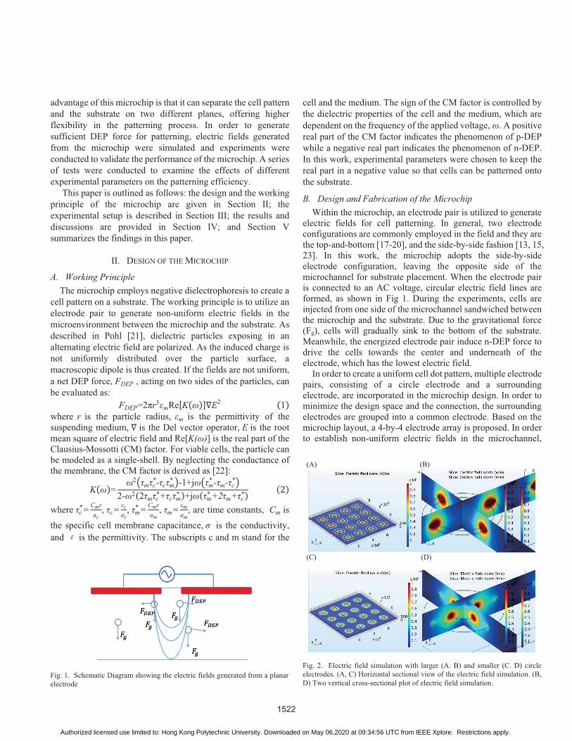
(A) (B)
(C) (D)
Fig. 2. Electric field simulation with larger (A. B) and smaller (C. D) circle
electrodes. (A, C) Horizontal sectional view of the electric field simulation. (B,
D) Two vertical cross-sectional plot of electric field simulation.
Fig. 1. Schematic Diagram showing the electric fields generated from a planar
electrode
1522
Authorized licensed use limited to: Hong Kong Polytechnic University. Downloaded on May 06,2020 at 09:34:56 UTC from IEEE Xplore. Restrictions apply.
Multiphysics software, COMSOL, was used to simulate the
results for analysis. In the simulation model, the circle
electrodes were modeled as a circular disk while the surrounding
electrode was modeled as a rectangular plane. The microchannel
was set with a height of 100 m that was filled with the medium.
Figure 2 shows the simulation of the electric field formed by the
microchip when a voltage was applied to the electrodes. The
high electric field is represented by the regions in red, which is
located at the gaps between the opposite electrodes. In contrast,
the low electric field is represented by the regions in blue, which
is located at the center of the circle electrode. The figures show
that the non-uniform electric field is successfully established
through the proposed electrode layout design. To explore the
effect of the electrode size, a simulation was performed with
larger and smaller circle electrodes. Comparing the results, the
field strength generated from smaller electrodes is weaker. Also,
the field distribution near the surrounding electrode is relatively
uniform, and cells may not experience the DEP effect. Hence,
reducing the electrode size will reduce the regions for cell
manipulation.
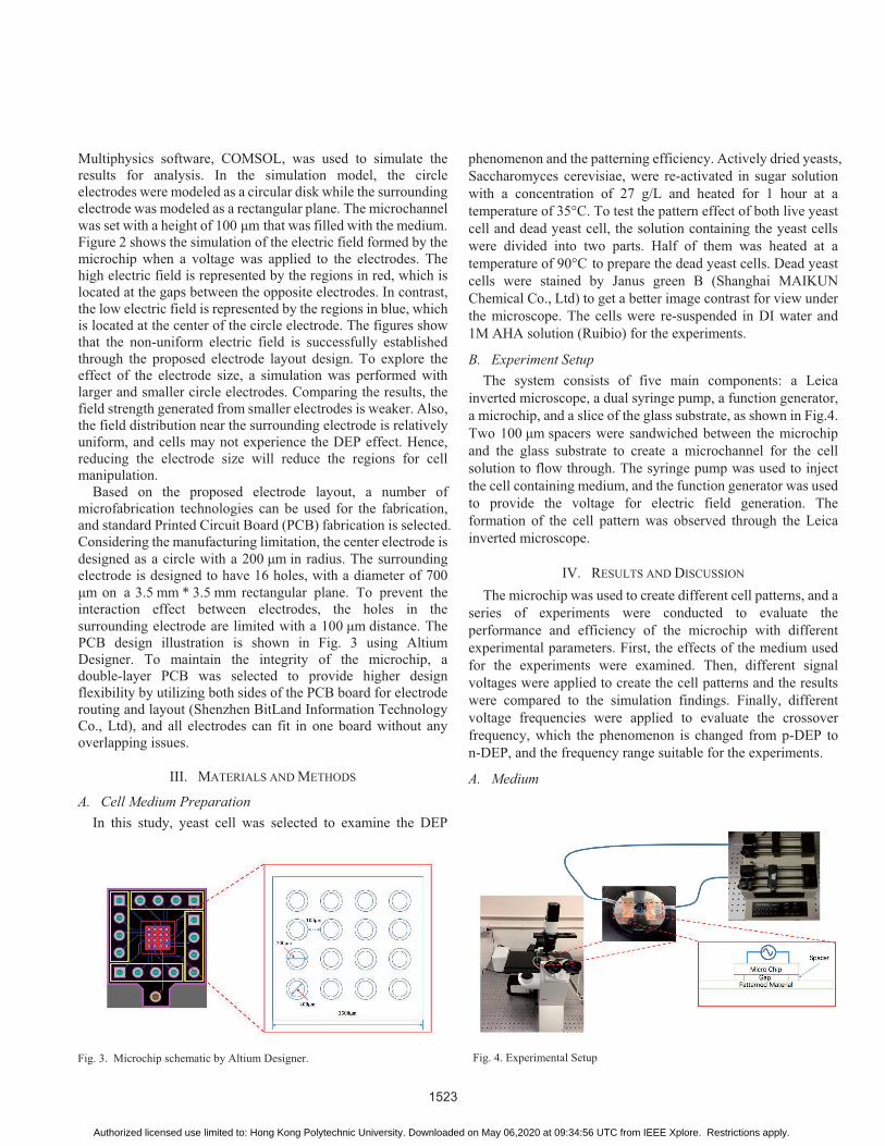
Based on the proposed electrode layout, a number of
microfabrication technologies can be used for the fabrication,
and standard Printed Circuit Board (PCB) fabrication is selected.
Considering the manufacturing limitation, the center electrode is
designed as a circle with a 200 m in radius. The surrounding
electrode is designed to have 16 holes, with a diameter of 700
m on a 3.5 mm * 3.5 mm rectangular plane. To prevent the
interaction effect between electrodes, the holes in the
surrounding electrode are limited with a 100 m distance. The
PCB design illustration is shown in Fig. 3 using Altium
Designer. To maintain the integrity of the microchip, a
double-layer PCB was selected to provide higher design
flexibility by utilizing both sides of the PCB board for electrode
routing and layout (Shenzhen BitLand Information Technology
Co., Ltd), and all electrodes can fit in one board without any
overlapping issues.
III. MATERIALS AND METHODS
A. Cell Medium Preparation In this study, yeast cell was selected to examine the DEP
phenomenon and the patterning efficiency. Actively dried yeasts,
Saccharomyces cerevisiae, were re-activated in sugar solution
with a concentration of 27 g/L and heated for 1 hour at a
temperature of 35°C. To test the pattern effect of both live yeast
cell and dead yeast cell, the solution containing the yeast cells
were divided into two parts. Half of them was heated at a
temperature of 90°C to prepare the dead yeast cells. Dead yeast
cells were stained by Janus green B (Shanghai MAIKUN
Chemical Co., Ltd) to get a better image contrast for view under
the microscope. The cells were re-suspended in DI water and
1M AHA solution (Ruibio) for the experiments.
B. Experiment Setup The system consists of five main components: a Leica
inverted microscope, a dual syringe pump, a function generator,
a microchip, and a slice of the glass substrate, as shown in Fig.4.
Two 100 m spacers were sandwiched between the microchip
and the glass substrate to create a microchannel for the cell
solution to flow through. The syringe pump was used to inject
the cell containing medium, and the function generator was used
to provide the voltage for electric field generation. The
formation of the cell pattern was observed through the Leica
inverted microscope.
IV. RESULTS AND DISCUSSION
The microchip was used to create different cell patterns, and a
series of experiments were conducted to evaluate the
performance and efficiency of the microchip with different
experimental parameters. First, the effects of the medium used
for the experiments were examined. Then, different signal
voltages were applied to create the cell patterns and the results
were compared to the simulation findings. Finally, different
voltage frequencies were applied to evaluate the crossover
frequency, which the phenomenon is changed from p-DEP to
n-DEP, and the frequency range suitable for the experiments.
A. Medium
Fig. 3. Microchip schematic by Altium Designer.
Fig. 4. Experimental Setup
1523
Authorized licensed use limited to: Hong Kong Polytechnic University. Downloaded on May 06,2020 at 09:34:56 UTC from IEEE Xplore. Restrictions apply.
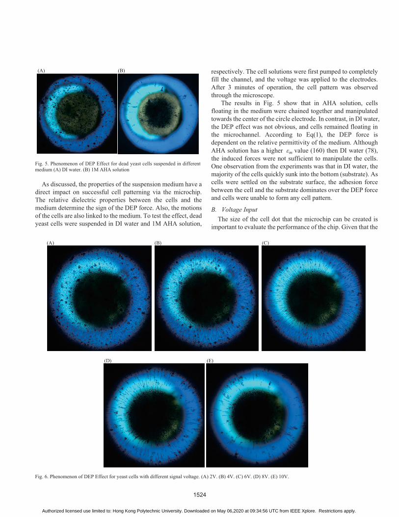
As discussed, the properties of the suspension medium have a
direct impact on successful cell patterning via the microchip.
The relative dielectric properties between the cells and the
medium determine the sign of the DEP force. Also, the motions
of the cells are also linked to the medium. To test the effect, dead
yeast cells were suspended in DI water and 1M AHA solution,
respectively. The cell solutions were first pumped to completely
fill the channel, and the voltage was applied to the electrodes.
After 3 minutes of operation, the cell pattern was observed
through the microscope.
The results in Fig. 5 show that in AHA solution, cells
floating in the medium were chained together and manipulated
towards the center of the circle electrode. In contrast, in DI water,
the DEP effect was not obvious, and cells remained floating in
the microchannel. According to Eq(1), the DEP force is
dependent on the relative permittivity of the medium. Although
AHA solution has a higher m value (160) then DI water (78),
the induced forces were not sufficient to manipulate the cells.
One observation from the experiments was that in DI water, the
majority of the cells quickly sunk into the bottom (substrate). As
cells were settled on the substrate surface, the adhesion force
between the cell and the substrate dominates over the DEP force
and cells were unable to form any cell pattern.
B. Voltage Input The size of the cell dot that the microchip can be created is
important to evaluate the performance of the chip. Given that the
(A) (B) (C)
(D) (E)
Fig. 6. Phenomenon of DEP Effect for yeast cells with different signal voltage. (A) 2V. (B) 4V. (C) 6V. (D) 8V. (E) 10V.
(A) (B)
Fig. 5. Phenomenon of DEP Effect for dead yeast cells suspended in different
medium (A) DI water. (B) 1M AHA solution
1524
Authorized licensed use limited to: Hong Kong Polytechnic University. Downloaded on May 06,2020 at 09:34:56 UTC from IEEE Xplore. Restrictions apply.
number of cells in the medium is fixed, a larger cell dot indicates
that the microchip is more effective to utilize the surrounding
cells to form the pattern at the center of the electrode. According
to Eq (1), the strength of the force is proportional to the gradient
of the square of the electric field. To explicitly examine the
effect of this parameter, voltage inputs of 2V, 4V, 6V, 8V, and
10V were applied to the microchip. The signal frequency was set
at 6MHz and the effects on dead yeast cells in 1M AHA solution
were shown in Fig. 6. As expected, when the voltage input is
low, cells that are far away from electric fields cannot be
manipulated due to the generation of a weaker DEP force. As the
voltage continues to increase, cell chains are formed along the
radial direction and the size of the cell dot is growing, as shown
in the figure. At a higher voltage, cells clustering at the center of
the electrode become more obvious. It can be noticed that most
of the cells suspending at the gap between the circle electrode
and the surrounding electrode are manipulated to form the cell
pattern, leaving a clear (cell-free) medium at the gap.
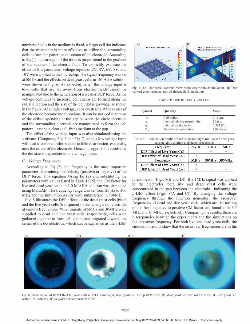
The effect of the voltage input was also simulated using the
software. Comparing Fig. 3 and Fig. 7, using a low voltage input
will lead to a more uniform electric field distribution, especially
near the center of the electrode. Hence, it supports the result that
the dot size is dependent on the voltage input.
C. Voltage Frequency According to Eq (2), the frequency is the most important
parameter determining the polarity (positive or negative) of the
DEP force. This equation Using Eq (2) and substituting the
parameters with values listed in Table I [15], the CM factor for
live and dead yeast cells in 1.0 M AHA solution was simulated
using MatLAB. The frequency range was set from 20 Hz to 300
MHz and the simulation results were summarized in Table II.
Fig. 8 illustrates the DEP effects of the dead yeast cells (blue)
and the live yeast cells (transparent) under a single dot electrode
at various frequencies. When signals of 5MHz and 30MHz were
supplied to dead and live yeast cells, respectively, cells were
gathered together to form cell chains and migrated towards the
center of the dot electrode, which can be explained as the n-DEP
phenomenon (Figs. 8(B and D)). If a 1MHz signal was applied
to the electrodes, both live and dead yeast cells were
concentrated in the gap between the electrodes, indicating the
p-DEP effect (Figs. 8(A and C)). By changing the voltage
frequency through the function generator, the crossover
frequencies of dead and live yeast cells, which are the turning
points from negative to positive CM factor, are found to be 3.5
MHz and 16 MHz, respectively. Comparing the results, there are
discrepancies between the experiments and the simulations on
the crossover frequency. For both live and dead yeast cells, the
simulation results show that the crossover frequencies are in the
(A) (B)
Fig. 7. (A) Horizontal sectional view of the electric field simulation. (B) Two
vertical cross-sectional plot of electric field simulation.
TABLE I: PROPERTIES OF YEAST CELL
Symbol Quantity Value
R Cell radius m
c Internal relative permittivity 50.6
c Internal conductivity 0.515 S/m
Cm Membrane capacitance 7.03 F/cm2
(A) (B) (C) (D)
Fig. 8. Phenomenon of DEP Effect for yeast cells in AHA solution (A) dead yeast cell with p-DEP effect. (B) dead yeast cell with n-DEP effect. (C) live yeast cell
with p-DEP effect. (D) live yeast cell with n-DEP effect.
TABLE II: Simulation results of the CM factor (sign) for live and dead yeast
cells in AHA solution at different frequencies
1525
Authorized licensed use limited to: Hong Kong Polytechnic University. Downloaded on May 06,2020 at 09:34:56 UTC from IEEE Xplore. Restrictions apply.
region of 100MHz, higher by an order of magnitude. The
simulation values are comparable to the one (108 Hz) reported in
[24] and [25], suggesting the single-shell model may not be
appropriate to describe yeast cells in AHA solution. Other cell
models, such as two-shell [26] or multi-shell model [27], should
also be considered to evaluate the optimal cell model to best
describe yeast cells. Despite the discrepancy, the crossover
frequency can be obtained through experiments and cell
patterning via n-DEP can be performed with a usable frequency.
It is known that the crossover frequency is unique to each cell
type and the medium, but similar tests can be performed on
different cell types to obtain the suitable frequency range for the
experiments.
V. CONCLUSION
In this study, a microchip consisting of a 4-by-4 dot electrode
array was designed and fabricated for cell patterning. This
microchip employed n-DEP and cell patterns were created on a
substrate lying on the microchip surface. The microchip was
fabricated using the PCB technique, and its performance was
examined through experiments using yeast cells. Results show
that the AHA solution is effective to minimize the amount of
cells sunk to the bottom. When a higher voltage is used, a larger
cell dot can be created. Also, the usable frequency from a
function generator can induce p-DEP and n-DEP force on live
and dead yeast cells, and a suitable frequency for the
experiments can be selected accordingly. This microchip
provides an easy and simple method to create cell patterns on a
substrate to facilitate cell assay and characterization.
REFERENCES
[1] . C. A. Vacanti, "History of tissue engineering and a glimpse into its future,"
Tissue engineering, vol. 12(5), pp. 1137-1142, 2006.
[2] . T. Yasukawa et al., "Electrophoretic cell manipulation and electrochemical
gene-function analysis based on a yeast two-hybrid system in a microfluidic
device," Analytical chemistry, vol. 80(10), pp. 3722-3727, 2008.
[3] . K. Ino, A. Ito, and H. Honda, "Cell patterning using magnetite nanoparticles
and magnetic force," Biotechnology and Bioengineering, vol. 97(5), pp.
1309-1317, 2007.
[4] . J. El-Ali, P. K. Sorger, and K. F. Jensen, "Cells on chips," (in eng), Nature, vol. 442(7101), pp. 403-11, Jul 27 2006.
[5] . H. Chu, Z. Huan, J. Mills, J. Yang, and D. Sun, "Three-dimensional cell
manipulation and patterning using dielectrophoresis via a multi-layer scaffold
structure," Lab on a Chip, vol. 15(3), pp. 920-930, 2015.
[6] . R. Amit, A. Abadi, and G. Kosa, "Characterization of steady streaming for a
particle manipulation system," Biomedical microdevices, vol. 18(2), p. 39, 2016.
[7] . M. Nagai, K. Kato, K. Oohara, and T. Shibata, "Pick-and-Place Operation of
Single Cell Using Optical and Electrical Measurements for Robust
Manipulation," Micromachines, vol. 8(12), p. 350, 2017.
[8] . S. Hu and D. Sun, "Automatic transportation of biological cells with a
robot-tweezer manipulation system," The International Journal of Robotics Research, vol. 30(14), pp. 1681-1694, 2011.
[9] . M. Okochi, S. Takano, Y. Isaji, T. Senga, M. Hamaguchi, and H. Honda,
"Three-dimensional cell culture array using magnetic force-based cell patterning
for analysis of invasive capacity of BALB/3T3/v-src," Lab on a chip, vol. 9(23),
pp. 3378-3384, 2009.
[10]. D. J. Collins, B. Morahan, J. Garcia-Bustos, C. Doerig, M. Plebanski, and
A. Neild, "Two-dimensional single-cell patterning with one cell per well driven
by surface acoustic waves," Nature communications, vol. 6, p. 8686, 2015.
[11]. B. Dura et al., "Profiling lymphocyte interactions at the single-cell level
by microfluidic cell pairing," Nature communications, vol. 6, p. 5940, 2015.
[12]. Z. R. Gagnon, "Cellular dielectrophoresis: applications to the
characterization, manipulation, separation and patterning of cells,"
Electrophoresis, vol. 32(18), pp. 2466-2487, 2011.
[13]. B. Yafouz, N. A. Kadri, and F. Ibrahim, "The design and simulation of a
planar microarray dot electrode for a dielectrophoretic lab-on-chip device,"
International Journal of Electrochemical Science, vol. 7(12), pp. 12054-12063,
2012.
[14]. M. Suzuki, T. Yasukawa, H. Shiku, and T. Matsue, "Negative
dielectrophoretic patterning with colloidal particles and encapsulation into a
hydrogel," Langmuir, vol. 23(7), pp. 4088-4094, 2007.
[15]. K. Ino, H. Shiku, F. Ozawa, T. Yasukawa, and T. Matsue, "Manipulation
of microparticles for construction of array patterns by negative dielectrophoresis
using multilayered array and grid electrodes," Biotechnology and bioengineering, vol. 104(4), pp. 709-718, 2009.
[16]. L.-C. Hsiung et al., "A planar interdigitated ring electrode array via
dielectrophoresis for uniform patterning of cells," Biosensors and Bioelectronics, vol. 24(4), pp. 869-875, 2008.
[17]. D. R. Albrecht, R. L. Sah, and S. N. Bhatia, "Geometric and material
determinants of patterning efficiency by dielectrophoresis," Biophysical Journal, vol. 87(4), pp. 2131-2147, 2004.
[18]. D. R. Albrecht, V. L. Tsang, R. L. Sah, and S. N. Bhatia, "Photo-and
electropatterning of hydrogel-encapsulated living cell arrays," Lab on a Chip, vol. 5(1), pp. 111-118, 2005.
[19]. H. Tsutsui et al., "Efficient dielectrophoretic patterning of embryonic
stem cells in energy landscapes defined by hydrogel geometries," Annals of biomedical engineering, vol. 38(12), pp. 3777-3788, 2010.
[20]. R. Z. Lin, C. T. Ho, C. H. Liu, and H. Y. Chang, "Dielectrophoresis
based cell patterning for tissue engineering," Biotechnology Journal: Healthcare Nutrition Technology, vol. 1(9), pp. 949-957, 2006.
[21]. H. A. Pohl, "Dielectrophoresis," The behavior of neutral matter in nonuniform electric fields, 1978.
[22]. T. Jones, "Electromechanics of ParticlesCambridge Univ," Press, Cambridge, 1995.
[23]. B. Yafouz, N. A. Kadri, and F. Ibrahim, "Dielectrophoretic manipulation
and separation of microparticles using microarray dot electrodes," Sensors, vol.
14(4), pp. 6356-6369, 2014.
[24]. G. Mernier, N. Piacentini, R. Tornay, N. Buffi, and P. Renaud, "Cell
viability assessment by flow cytometry using yeast as cell model," Sensors and Actuators B: Chemical, vol. 154(2), pp. 160-163, 2011.
[25]. S.-Y. Tang, W. Zhang, S. Baratchi, M. Nasabi, K. Kalantar-zadeh, and K.
Khoshmanesh, "Modifying dielectrophoretic response of nonviable yeast cells
by ionic surfactant treatment," Analytical chemistry, vol. 85(13), pp. 6364-6371,
2013.
[26]. Z. Gagnon, J. Mazur, and H.-C. Chang, "Integrated AC electrokinetic cell
separation in a closed-loop device," Lab on a Chip, vol. 10(6), pp. 718-726,
2010.
[27]. S. Gupta, R. G. Alargova, P. K. Kilpatrick, and O. D. Velev, "On-chip
electric field driven assembly of biocomposites from live cells and
functionalized particles," Soft Matter, vol. 4(4), pp. 726-730, 2008.
1526
Authorized licensed use limited to: Hong Kong Polytechnic University. Downloaded on May 06,2020 at 09:34:56 UTC from IEEE Xplore. Restrictions apply.