Embed Size (px)
Citation preview
Leif Halbo and Per Ohlckers: Electronic Components, Packaging and Production
6. 1
CHAPTER 6
PRINTED CIRCUIT BOARD DESIGN 6.1 INTRODUCTION The designers are key personnel in the development of a new electronic product but
they are not the only ones. A successful product depends on an intimate co-operation between specialists from many fields. Their common goal is to make a product with the right quality at the right price.
General circuit design is outside the scope of this book. However, we shall discuss
those aspects of the design connected to choice of technology, components, PWB layout and production on PCB/hybrid circuit level. (For hybrid circuit design, including polymer thick film circuits, see also Chapter 8.)
The design is generally performed on a CAD system. After entering the netlist and the
components, the circuit diagram is worked out. Information and symbols for each component are stored in the CAD system component library. Instead of experimenting with hardware models more and more is done by computer simulations, as the circuit complexity and speed of operation increases.
The layout or PWB design is simplified by more or less automatic routing performed
by the CAD system. Still, critical information about placement of certain components, electromagnetic compatibility (EMC), thermal limitations, etc., is manually entered by the designer.
From the CAD system we get the schematic, assembly drawings and other
documentation, data for photo- or laser plotter to manufacture photographic films for the PWB production, data for the printing mask for solder resist and solder paste printing, data for numeric drilling and milling machines, placement information for pick and place machines, data for test fixtures and the testing machine, etc. (Please refer to. Section 5.3).
6.2 GENERAL GUIDELINES 6.2.1 Right quality It is essential to design for right quality. This implies that the product must satisfy all
specifications regarding electrical performance, reliability and product operating lifetime, ergonometry, etc. but the product should not be over-specified and thus unnecessarily costly. To achieve this it is important to: - Choose the best suitable technology or combination of technologies, and
an optimal partitioning - Choose components with the right reliability and suitable packaging - Design for manufacture - Design for testability - Design for ease of repair, etc.

Leif Halbo and Per Ohlckers: Electronic Components, Packaging and Production
6. 2
The contact between the designers, testing people and the production department is formalised in "design review", after which the test specialists have accepted the design concerning testability, the production people have taken part in planning how the product will be produced and accepted the design concerning manufacturability in the available production line, etc. If the PWBs or printed circuit boards are to be produced by subcontractors, they must also participate in the planning, to insure that the product is fit for their production equipment. Otherwise, modifications or a re-design may be needed later, resulting in delays and extra cost.
Fig. 6.1: Proper component placement for hole- and surface mounted components
[6.1, 6.2].

Leif Halbo and Per Ohlckers: Electronic Components, Packaging and Production
6. 3
6.2.2 Design for manufacture By "manufacturability" we also mean that it is fit for robot mounting if it is planned,
that components and materials can withstand the solder processes to be used, etc. High yield, low cost production requires, for example:
- As few conductor layers as possible in the PWB. - As coarse conductor pattern as possible (no fine line). - As few component types as possible (standardisation). - Robust electrical design (no tight tolerances).
Standardisation of the PWB sizes is of importance, to make them fit into standard
cabinets, and to utilise the panel sizes effectively. The components should be placed orderly, polarised components (diodes, electrolytic
capacitors, ICs, etc.) oriented the same way when possible, see Figure 6.1. This gives the highest component density and most efficient assembly process, and it makes visual inspection easier.
6.2.3 Electromagnetic compatibility (EMC) Wires and current loops on the PCB and in the electric system will act as antennas,
emitting electromagnetic radiation that may interfer with radio communication and other electronic equipment. Likewise, the same elements of a system will act as receiver antennas for radiation, and incoming radiation may disturb the functioning of the system. It is essential that electronics are designed for low electromagnetic emission and high immunity. Besides radiation, the equipment must also be designed for low emission of noise on the power grid as well as high immunity for incoming noise. These factors are called ElectroMagnetic Compatibility (EMC), and disturbances called ElectroMagnetic Interference (EMI).
There are a number of international EMC standards that must be met by electronic
equipment [6.0]. The emission is often caused by [6.0]:
- A conductor loop on a PCB, acting as a magnetic antenna, generating a field proportional to the current and the area of the loop.
- A conductor with a voltage drop, acting as a rod antenna.
Good EMC design is a large field and the reader should consult the specialised literature. However, some basic rules should be considered: - Use a ground plane. - Use compact component technology (SMT) and compact layout to
reduce current loop areas. - Do not use fast component technology (short rise-/fall times) and high
clock frequency unless necessary. - Use decoupling capacitors where appropriate.
Modifications of existing equipment to fulfil EMC standards are a lot more expensive
and time consuming than making a good EMC design from the start.

Leif Halbo and Per Ohlckers: Electronic Components, Packaging and Production
6. 4
6.3 HOLE AND SURFACE MOUNTED PCBs 6.3.1 Minimum dimensions The conductors cross sectional area determines the maximum current in a conductor
without excessive heating of the conductor and the PCB. Figure 6.2 shows the temperature increase as a function of current and conductor cross section. The data is based on convection heat transfer to the surrounding air, and lateral heat conduction primarily in the Cu foil.
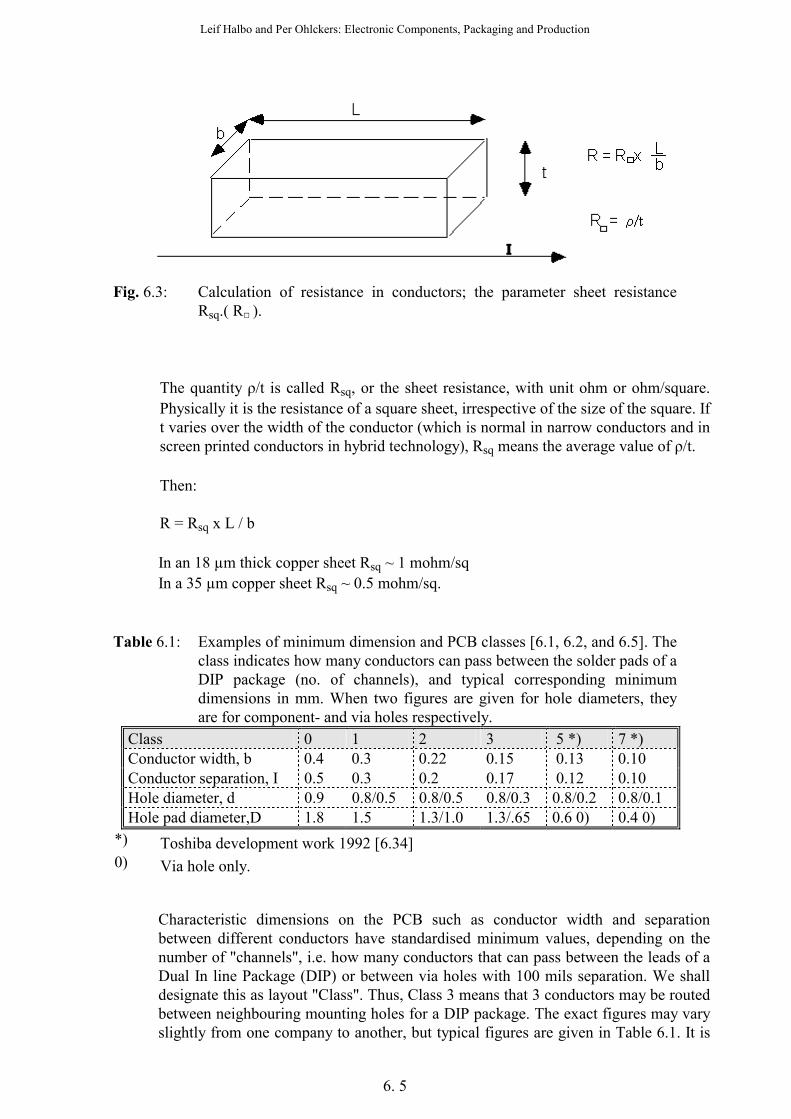
The voltage drop in a long narrow conductor may also be of importance. It is given by
(Figure 6.3): R = ρ x L/(t x b) where ρ is the resistivity in the copper layer, approximately 2.0 x 10 -8 ohm m for
rolled copper at room temperature.
Fig. 6.2: Current capacity and temperature increase in conductors on PCBs [6.1,
6.3]. The lower figure shows the conductor cross-section (along the x-axis) as a function of the conductor width for different Cu-layer thicknesses. The upper figure shows the temperature increase (labels on each curve) at different combinations of cross-sections and currents).
Leif Halbo and Per Ohlckers: Electronic Components, Packaging and Production
6. 5
Fig. 6.3: Calculation of resistance in conductors; the parameter sheet resistance
Rsq.( R□ ). The quantity ρ/t is called Rsq, or the sheet resistance, with unit ohm or ohm/square.
Physically it is the resistance of a square sheet, irrespective of the size of the square. If t varies over the width of the conductor (which is normal in narrow conductors and in screen printed conductors in hybrid technology), Rsq means the average value of ρ/t.
Then: R = Rsq x L / b In an 18 µm thick copper sheet Rsq ~ 1 mohm/sq In a 35 µm copper sheet Rsq ~ 0.5 mohm/sq. Table 6.1: Examples of minimum dimension and PCB classes [6.1, 6.2, and 6.5]. The
class indicates how many conductors can pass between the solder pads of a DIP package (no. of channels), and typical corresponding minimum dimensions in mm. When two figures are given for hole diameters, they are for component- and via holes respectively.
Class 0 1 2 3 5 *) 7 *) Conductor width, b 0.4 0.3 0.22 0.15 0.13 0.10 Conductor separation, I 0.5 0.3 0.2 0.17 0.12 0.10 Hole diameter, d 0.9 0.8/0.5 0.8/0.5 0.8/0.3 0.8/0.2 0.8/0.1 Hole pad diameter,D 1.8 1.5 1.3/1.0 1.3/.65 0.6 0) 0.4 0)
*) Toshiba development work 1992 [6.34] 0) Via hole only.
Characteristic dimensions on the PCB such as conductor width and separation
between different conductors have standardised minimum values, depending on the number of "channels", i.e. how many conductors that can pass between the leads of a Dual In line Package (DIP) or between via holes with 100 mils separation. We shall designate this as layout "Class". Thus, Class 3 means that 3 conductors may be routed between neighbouring mounting holes for a DIP package. The exact figures may vary slightly from one company to another, but typical figures are given in Table 6.1. It is

Leif Halbo and Per Ohlckers: Electronic Components, Packaging and Production
6. 6
important to make a distinction between the dimensions defined in the CAD station and the dimensions on the PCB. This is due to underetching (see Section 5.8).
Larger dimensions than the minimum values should be used whenever possible in
order to raise the production yield. Figure 6.4 shows the separations between solder area and solder resist. The solder
resist is usually screen-printed for layout in Classes 0 and 1. Therefore, it is necessary to have a relatively large separation due to the limitations in the screen printing process. In class 2 or higher, a photo-processed solder resist is used (see Section 5.6). Photo-processed solder resist must be used if conductors are to pass between the terminals of a surface mount component. If a dry film is used it may be advantageous to cover the vias, ("tenting", see Figure 5.6 b) in order to prevent the solder from entering the vias [6.1].
Fig. 6.4: a): Parameters in layout dimensions used in Table 6.1. b): Minimum
dimensions for solder mask for surface mount PWBs. Left: Dimensions for screen printed solder mask, with one common opening for all solder lands of an IC package, right: photoprocessible solder mask with a "pocket" for each terminal, permitting conductors between the solder lands [6.2].
6.3.2 Different PCBs and limitations on components and solder process's The most common combinations of components on the two sides of hole- and surface
mounted PCBs are shown in Figure 6.5. The components are soldered by a combination of reflow- and wave solder processes. Wave soldering may be done on the secondary side only.

Leif Halbo and Per Ohlckers: Electronic Components, Packaging and Production
6. 7
Fig. 6.5: Common types of SMD- and mixed SMD-/hole mount PCBs. Not all surface mount components can withstand the thermal shock represented by a
solder wave. Furthermore, solder bridges between the leads may be encountered due to the lead shape, component body shape or small lead pitch. It is therefore recommended that all SMD ICs are reflow soldered, or at least LLCCs and the other packages with terminals on all four sides. Special types of wave soldering equipment may enable wave soldering on different types of SMD ICs, such as SO packages (please refer to Section 7.3).
Through hole mounted components normally cannot withstand the temperature of
wave soldering. They are therefore mounted on the primary side only, or they are manually mounted and manually soldered after machine soldering is completed. Neither can they withstand the reflow soldering process, and therefore the wave soldering must be done after the reflow soldering.
These constraints must be considered during the design process. Some of the
production process details for the different PCB configurations will be discussed in Sections 7.3 and 7.5.
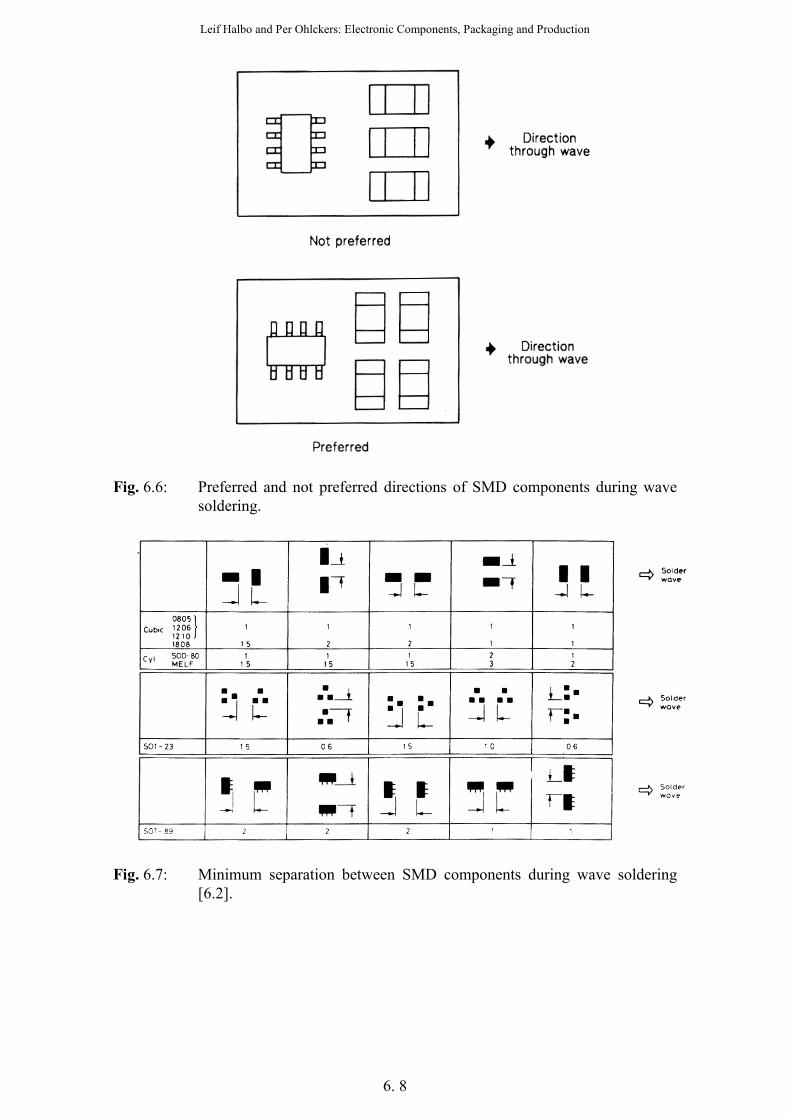
SMD components that are wave soldered have a preferred orientation with respect to
the solder wave, see Figure 6.6. Solder bridges, non-wetted areas and the effect of "shadowing" are reduced in this way (see Section 7.3). The shadowing effect is more pronounced for tall packages. There should be a minimum distance between components, see Figure 6.7. The reasons are: - Reducing solder bridging - Take care of tolerances in component size - Necessary space for the mounting head of the pick and place equipment - Tolerances in the placement accuracy - Ease of repair, visual inspection, space for de-soldering equipment, etc.
Leif Halbo and Per Ohlckers: Electronic Components, Packaging and Production
6. 8
Fig. 6.6: Preferred and not preferred directions of SMD components during wave
soldering.
Fig. 6.7: Minimum separation between SMD components during wave soldering
[6.2].

Leif Halbo and Per Ohlckers: Electronic Components, Packaging and Production
6. 9
6.3.3 Some general rules The PWB should include 2 - 3 guiding holes and registration marks for accurate
positioning in the production equipment. Solder lands should be thermally isolated from large Cu-foil areas by limiting their
extension as shown in Figure 6.8. The solder mask should cover all area except the solder lands (and hole pads), to prevent the solder from spreading during reflow. Tracks should approach the solder lands symmetrically and perpendicularly (90o angles).
Fig. 6.8: Solder lands for SMD components should be separated from heavy copper
areas by narrow constrictions. Conductors should preferably leave the solder lands of one component symmetrically.
Fig. 6.9: Via holes should be separated from solder lands.
Leif Halbo and Per Ohlckers: Electronic Components, Packaging and Production
6. 10
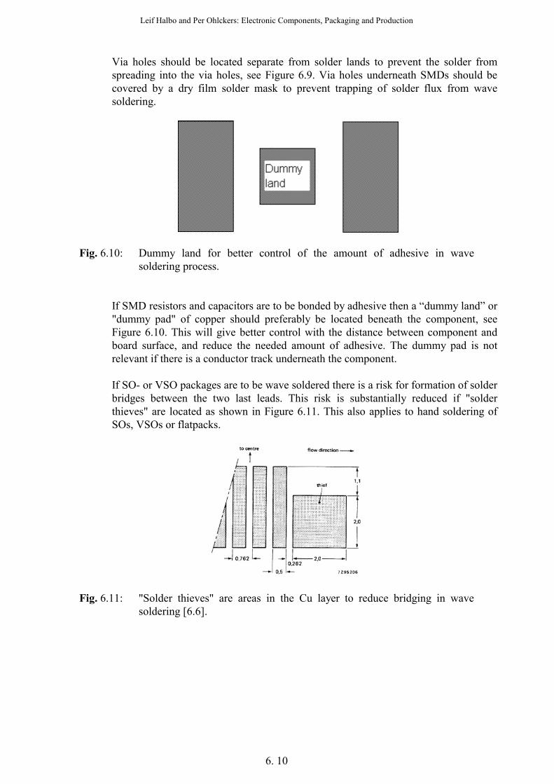
Via holes should be located separate from solder lands to prevent the solder from
spreading into the via holes, see Figure 6.9. Via holes underneath SMDs should be covered by a dry film solder mask to prevent trapping of solder flux from wave soldering.
Fig. 6.10: Dummy land for better control of the amount of adhesive in wave
soldering process. If SMD resistors and capacitors are to be bonded by adhesive then a “dummy land” or
"dummy pad" of copper should preferably be located beneath the component, see Figure 6.10. This will give better control with the distance between component and board surface, and reduce the needed amount of adhesive. The dummy pad is not relevant if there is a conductor track underneath the component.
If SO- or VSO packages are to be wave soldered there is a risk for formation of solder
bridges between the two last leads. This risk is substantially reduced if "solder thieves" are located as shown in Figure 6.11. This also applies to hand soldering of SOs, VSOs or flatpacks.
Fig. 6.11: "Solder thieves" are areas in the Cu layer to reduce bridging in wave
soldering [6.6].

Leif Halbo and Per Ohlckers: Electronic Components, Packaging and Production
6. 11
6.3.4 Dimensions of solder lands It is important to use optimal dimensions and positions for the solder lands to
minimise solder defects and optimise strength and reliability in the solder joints. The optimal choice depends on a number of parameters, such as: - Adhesive- and solder process and equipment, dimensions of the
components and their tolerances (typically +/- 0.1 - 0.2 mm). - Dimension tolerances in PWB (0.05 - 0.15 mm), and in the solder
printing process. - Conductor line widths and tolerances (0.1 - 0.2 mm). - Pick and place equipment and placement tolerances (0.05 - 0.2 mm). - Visual inspection. - Density of components. - Repair procedures. - CAD equipment, standardisation, etc.
The importance of some of these tolerances is reduced if electronic pattern recognition is used. Many of these parameters are different for different manufacturers and even between different products and production lines for the same manufacturer. The dimensions for a specific component may vary considerably between different manufacturers.
One may therefore frequently encounter different recommended design rules for each
specific component, (see, e.g. [6.2, 6.4-6.9]). Rectangular solder lands or rectangular lands with rounded corners are used for
SMDs. Rounded corners are preferred for photo plotting because a larger aperture may be used. In the wave solder process larger solder lands are used than for reflow soldering, to improve wetting and prevent the shadow effect (Section 7.3). It is common practice, in wave soldering, to use solder lands slightly wider than the component itself for narrow components. Some manufacturers use solder lands considerably narrower than the component, however. This gives a smaller solder fillet with less mechanical stress and improved reliability, but it requires more accurate component placement. For wide components narrow solder lands should always be used to avoid excessively big solder fillets.
Fig. 6.12: Parameters defining solder land dimensions for SMD resistors and
capacitors, please refer to Table 6.2.

Leif Halbo and Per Ohlckers: Electronic Components, Packaging and Production
6. 12
Figures 6.12 and 6.13 show some different parameters describing the PWB layout for passive components and Table 6.2 shows recommended dimensions. These and the following recommendations are based on [6.2, 6.4 - 6.5] and the experience from ABB plants. In the case of components with known dimensions, not shown in the table, the following empirical expressions may be employed, see Figure 6.13 [6.4, 6.8]:
Fig. 6.13: Additional dimensions of SMD component and solder lands.
Table 6.2: Solder land dimensions for SMD resistors and capacitors (mm), please
refer to Figure 6.12. Wave soldering Reflow soldering Type Size a b B a b B 0603 0.9 0.8 2.3 *) Chip 0805 1.45 1.2 3.65 1.45 0.8 2.65 resistors 1206 1.7 1.4 4.85 1.7 1.0 3.65 and 1210 2.75 1.4 4.85 2.75 1.0 3.6 capacitors 1808 2.25 1.5 6.45 2.25 1.1 5.2 1812 3.25 1.5 6.45 3.25 1.1 5.2 2220 5.3 1.6 7.6 5.3 1.2 6.2 Al electrolytic 1a 2.5 2.0 10.0 2.5 3.0 9.0 capacitors (Philips) 1 2.5 2.0 14.0 2.5 3.0 12.0 Tantalum a 1.5 2.0 5.0 1.5 1.1 3.2 electrolytic b 1.5 2.0 6.3 1.5 1.1 4.5 capacitors c 1.5 2.0 7.55 1.5 1.1 5.75 (Philips) d 2.75 2.0 6.3 2.75 1.1 4.5 e 2.75 2.0 7.55 2.75 1.1 5.75 f 3.65 2.2 8.45 3.65 1.3 6.65 g 3.0 2.5 9.15 3.0 1.6 7.35 h 4.0 2.5 9.65 4.0 1.6 7.85
*) Solder land dimensions of 0603 components are discussed in [6.35] Width of solder land: a = Wmax+ K Length of solder land: - Reflow soldering: b = Hmax + 2Tmax + K - Wave soldering: b = Hmax + 2Tmax + 2K Total length: B = Lmax + 2Hmax + 2Tmax + K,

Leif Halbo and Per Ohlckers: Electronic Components, Packaging and Production
6. 13
Where the subscript maximum means the maximum component dimension inside the
tolerance and K = 0.25 mm. Recommended layout for diodes and transistors is shown in Figure 6.14.
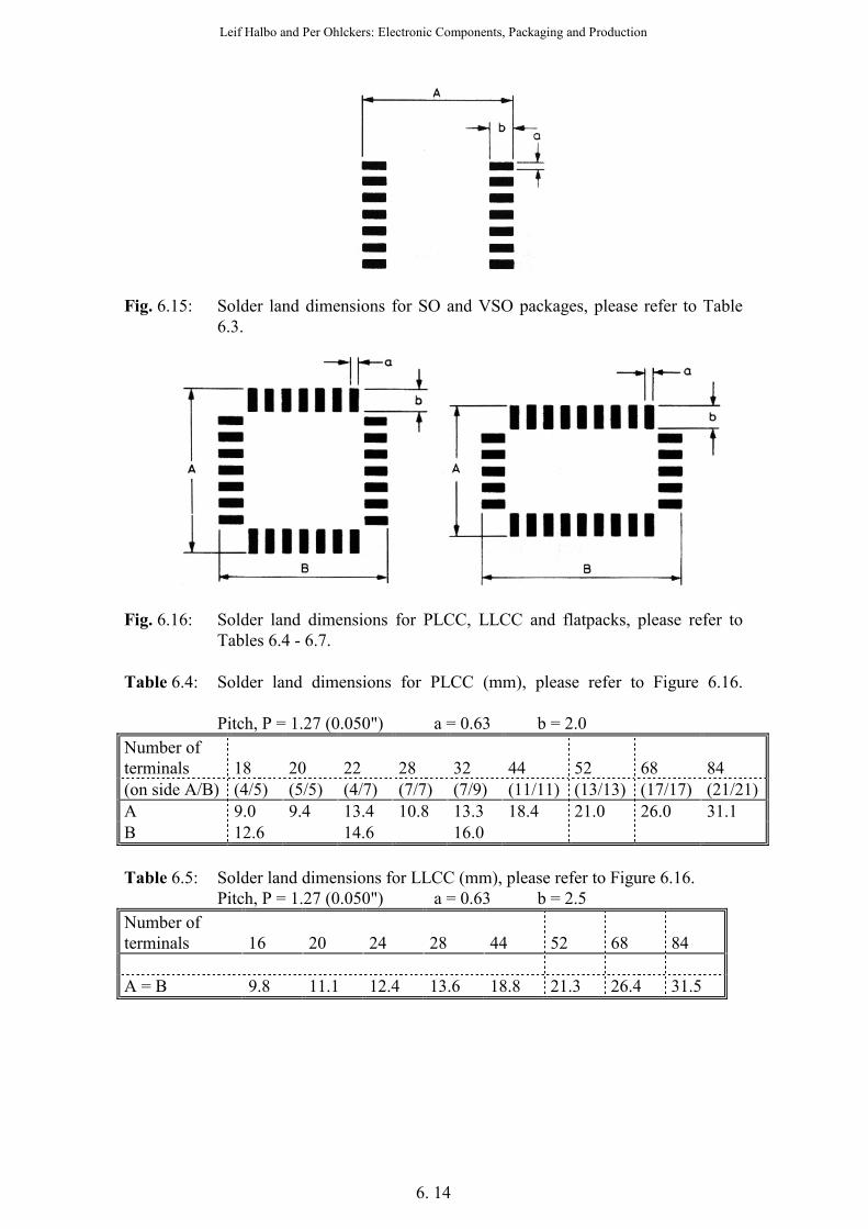
Fig. 6.14: Solder land dimensions for SMD transistors and diodes [6.2]. Table 6.3: Solder land dimensions for SO or VSO components (mm), please refer to
Figure 6.15. Package Pitch, P a b A SO-8 to -16 1.27 0.63 1.5 7.2 SO-16L to -28 1.27 0.63 1.8 11.6 VSO -40 0.76 0.4 2.7 13.6
Leif Halbo and Per Ohlckers: Electronic Components, Packaging and Production
6. 14
Fig. 6.15: Solder land dimensions for SO and VSO packages, please refer to Table
6.3.
Fig. 6.16: Solder land dimensions for PLCC, LLCC and flatpacks, please refer to
Tables 6.4 - 6.7. Table 6.4: Solder land dimensions for PLCC (mm), please refer to Figure 6.16.
Pitch, P = 1.27 (0.050") a = 0.63 b = 2.0 Number of terminals
18
20
22
28
32
44
52
68
84
(on side A/B) (4/5) (5/5) (4/7) (7/7) (7/9) (11/11) (13/13) (17/17) (21/21) A 9.0 9.4 13.4 10.8 13.3 18.4 21.0 26.0 31.1 B 12.6 14.6 16.0
Table 6.5: Solder land dimensions for LLCC (mm), please refer to Figure 6.16. Pitch, P = 1.27 (0.050") a = 0.63 b = 2.5 Number of terminals
16
20
24
28
44
52
68
84
A = B 9.8 11.1 12.4 13.6 18.8 21.3 26.4 31.5
Leif Halbo and Per Ohlckers: Electronic Components, Packaging and Production
6. 15
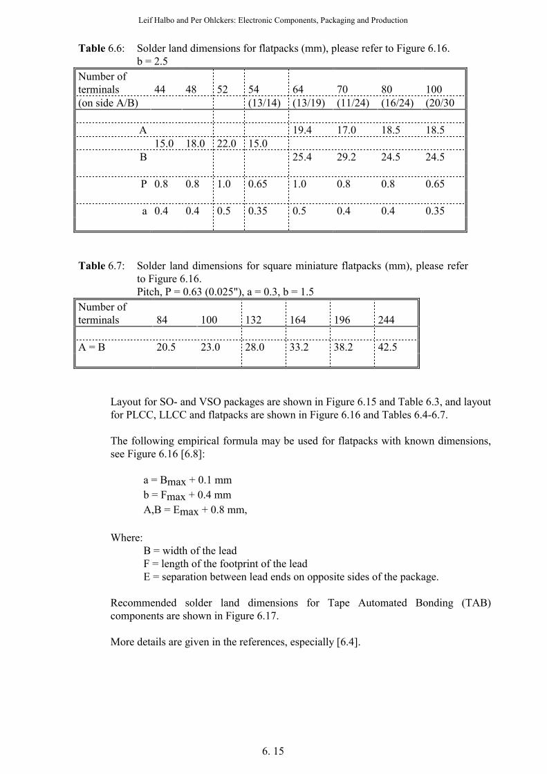
Table 6.6: Solder land dimensions for flatpacks (mm), please refer to Figure 6.16. b = 2.5 Number of terminals
44
48
52
54
64
70
80
100
(on side A/B) (13/14) (13/19) (11/24) (16/24) (20/30
A 19.4 17.0 18.5 18.5 15.0 18.0 22.0 15.0
B 25.4 29.2 24.5 24.5
P 0.8 0.8 1.0 0.65 1.0 0.8 0.8 0.65
a 0.4 0.4 0.5 0.35 0.5 0.4 0.4 0.35
Table 6.7: Solder land dimensions for square miniature flatpacks (mm), please refer to Figure 6.16.
Pitch, P = 0.63 (0.025"), a = 0.3, b = 1.5 Number of terminals
84
100
132
164
196
244
A = B 20.5 23.0 28.0 33.2 38.2 42.5 Layout for SO- and VSO packages are shown in Figure 6.15 and Table 6.3, and layout
for PLCC, LLCC and flatpacks are shown in Figure 6.16 and Tables 6.4-6.7. The following empirical formula may be used for flatpacks with known dimensions,
see Figure 6.16 [6.8]:
a = Bmax + 0.1 mm b = Fmax + 0.4 mm A,B = Emax + 0.8 mm,
Where:
B = width of the lead F = length of the footprint of the lead E = separation between lead ends on opposite sides of the package.
Recommended solder land dimensions for Tape Automated Bonding (TAB) components are shown in Figure 6.17.
More details are given in the references, especially [6.4].

Leif Halbo and Per Ohlckers: Electronic Components, Packaging and Production
6. 16
Fig. 6.17: Solder land dimensions for TAB [6.10]. 6.3.5 Design of printing screens for solder paste The correct amount of solder paste is important for strength and reliability of the
solder joints. A suitable amount of solder paste for discrete components and IC's with 50 mil pitch is obtained by depositing a 175-200 µm high layer of solder paste over the whole solder land area. It may be an advantage to use a thicker layer over a reduced area, if a thick dry film solder mask is used.
A smaller amount of solder paste should be used on ICs with finer pitch to avoid
solder bridges [6.11]. Either a reduced area of the screen opening may be used, or a thinner screen. See also Section 7.3. In the thermode soldering process (Section 7.3) less solder should be used than in the normal reflow soldering process.
If TAB circuits are used, the solder is normally applied by electroplating [6.10, 6.11]. 6.4 DESIGN FOR TESTABILITY Careful production testing is important to avoid sending faulty products onto the
market, which may lead to great expenses and loss of reputation and market share. For complex products the testing may be time consuming and cost nearly as much as the rest of the production. Still it may not be practical to have a test that will detect all possible faults. The test effectiveness is described by: DL (ppm) = 1 - Y(1-T) x 106

Leif Halbo and Per Ohlckers: Electronic Components, Packaging and Production
6. 17
where : DL = Defect level: the fraction of delivered products that contains faults. Y = Yield = 1 - (Probability of producing a faulty product). T = Fault coverage: The probability that an existing fault is detected in
the testing. Thus, to minimise the defect level it is important to have a high production yield
(few faults produced), and a test procedure giving a high fault coverage. Designers and test specialists should co-operate intimately during product design to develop a good test strategy.
There are two main test principles: Functional test and in-circuit test. 6.4.1 Functional test In this test method electrical signals typical of the operation of the circuit are applied
to the connectors on the PCB. The responses to these signals are recorded and compared to the correct response.
Advantages of functional test:
- The components are tested in their operating environment. - Design faults may be found. - Timing problems may be found.
Disadvantages of functional testing:
- Necessary software development is time consuming. - Requires highly skilled personnel. - Will normally not localise the fault. - Long testing time. - New faults may be generated in the test. - Limited fault coverage.
6.4.2 In-circuit test In this test method each component is tested individually with test probes.
Neighbouring components must be isolated by guarding techniques in analogue circuits or latching in digital circuits [6.3].
Advantages of in-circuit testing:
- Short testing time: The test localises the fault. - Many faults may be found simultaneously. - Less time consuming software development. - The PCB does not need to be powered up, and the danger of generating
faults by the test is reduced.
Disadvantages: - Time consuming test. - The interactions between components are not tested. - Require expensive test fixture. - Access to all nodes in the circuit is necessary.
Leif Halbo and Per Ohlckers: Electronic Components, Packaging and Production
6. 18
The circuit complexity and production volume are important factors in the decision of test method. Therefore the typical extra board area needed for the test points for in circuit testing is less than 5 %, and the cost of area is rarely an important argument against in-circuit test. A combination of the two methods is also common: Smaller functional blocks may be functionally tested, and critical components may be in-circuit tested.
6.4.3 Design for improved testability The testing time may be reduced and the fault coverage increased by designing in
additional electronic functions on the board, explicitly for optimising the testing. Among the methods are "Level sensitive scan design", "Scan path", "Boundary scan", "Built-in self test" [6.12, 6.14].
6.4.4 Guidelines Some guidelines for test strategy:
- Use single sided testing if at all possible. Double sided test fixtures (see Section 7.6) are expensive and less robust.
- The testing should be made on separate test points, not on the component leads or solder lands, please refer to Figure 6.18.
- The test points should preferably be located on a 0.1" grid, please refer to Figure 6.19. They ought to be 0.9 mm or more in diameter. Test probes for 0.05" pitch test points are easily damaged during the testing. False faults will be recorded, and the test fixture must be frequently repaired. If it is necessary to use 0.05 "pitch testing, it should be limited to the minimum necessary test points.
- The test points should be covered by solder to obtain reliable contact, and not be covered by solder mask.
- The height of high components on the testing side of the board must be considered when the test fixture is designed.
The testing is a major cost in complex products and it is good practice to plan test procedures early in the product development phase. Production volumes, expected type of faults, test software and hardware development costs and board time in the test equipment are important issues to consider. A computer integrated interface between test development and other design activities will lead to cost reduction and fewer errors in information exchange between different design and development activities. This is a part of computer integrated manufacturing (CIM).

Leif Halbo and Per Ohlckers: Electronic Components, Packaging and Production
6. 19
Fig. 6.18: a): Correct position of test point, separated from solder land. b): Test
points on solder lands are not recommended. c): Testing on components or component leads should be avoided.
Fig. 6.19: Examples of test point placement on a grid with 0.1” spacing, for testing
of SMD components with 0.05” pitch [6.4]. In addition to the product test described, a new design will be stress tested for
verification of the reliability of the design. This will be described in Chapter 9.

Leif Halbo and Per Ohlckers: Electronic Components, Packaging and Production
6. 20
6.5 MATERIALS CONSIDERATIONS FOR THERMAL COMPATIBILITY Combinations of materials with different TCEs may give rise to strain and mechanical
stress. The problem increases with the size of the components, the magnitude of the difference in the TCEs, and the temperature variations, Figure 6.20.
SMD resistors and many capacitors have bodies of ceramic. Due to their small size
they may normally be soldered onto organic substrates (PWBs) without thermal mismatch problems. Leadless ceramic ICs (LLCCs) with sides less than approximately 10 mm (28 terminals or less), may be soldered onto organic boards in less demanding environments. For larger LLCCs we have the following alternatives: - Socket mounting - Soldering of leads onto the components (provided it is suitable for it,
please refer to Section 4.5) - Use of PWB with a compliant organic surface layer (marginal
improvement only) - Use of PWB with low TCE metal core (please refer to Section 5.9) - Use of ceramic substrate (daughter board/thick film hybrid circuit).
Fig. 6.20: Mechanical strain is caused by difference in coefficient of thermal
expansion (TCE), and changes in temperature. The magnitude of the corresponding stress depends on dimensions, temperature difference/change, and the elastic moduli of the materials.
In many cases it is possible to use leaded IC packages as an alternative to LLCCs (Section 4.5).

Leif Halbo and Per Ohlckers: Electronic Components, Packaging and Production
6. 21
6.6 THERMAL DESIGN 6.6.1 Why thermal design? Miniaturisation is a major trend in current electronic design. In most cases this results
in higher heat dissipation per volume and higher temperatures in the components unless thermal design is emphasised.
The essence of thermal design is to assure, during the design phase, that all
components operate within specified temperature limits. Selection of components, packages, component layout, PWB materials, cooling fins, fans, etc. is part of the thermal design.
An important reason for doing thermal design is the fact that increasing operating
temperature results in shorter expected operating life. Typically for electronic products, a 10°C temperature increase reduces the life
length by 50%. This is often discussed in terms of Arrhenius equation [6.16 - 6.18]. For materials with thermal mismatch the time to failure will often decrease when
cyclic temperature variations increase. The main purpose of thermal design is to obtain a sufficiently high reliability at the
lowest possible cost. 6.6.2 Heat transport Heat generated in the components must be transported away to the ambient
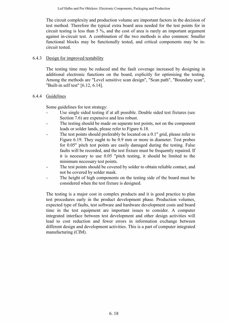
environment. There are three fundamental modes of heat transportation: conduction, convection and radiation, Figure 6.21. The two first modes are most important, and for SMDs the heat conduction dominates (unless forced air circulation is used).
Leif Halbo and Per Ohlckers: Electronic Components, Packaging and Production
6. 22
Fig. 6.21: a): Heat flow from hole mounted and surface mounted components on a
PCB. b): Relative amount of heat removed by conduction, convection and radiation, from DIP hole mounted components and SMD LLCC components - typical values.
Leif Halbo and Per Ohlckers: Electronic Components, Packaging and Production
6. 23
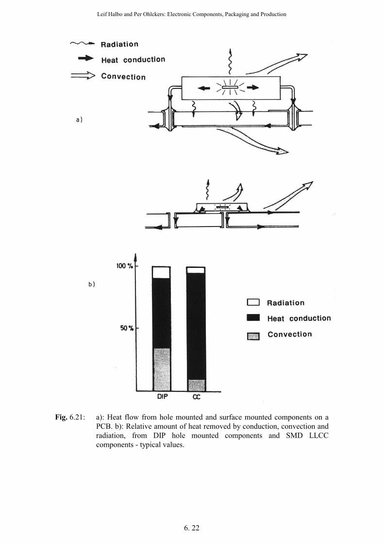
Fig. 6.22: a): Heat flow due to conduction - Fourier´s equation. b): Heat flow due to
convection. Fourier´s law describes heat conduction, see Figure 6.22: Q = ∆T/RT
Where: RT = 1/K x L/A , and: Q = Heat flow (W) ∆T = Temperature difference (°C) RT = Thermal resistance (°C/W) K = Thermal conductivity (W/m°C) L, A = Length and cross-sectional area of the thermal conductor Fourier´s law is equivalent to Ohm's law for electrical conduction: I = ∆U/Rel Where: Rel = 1/σ x L/A Heat transport by convection is described by: Q = h x A x ∆T Where: h = convection coefficient (W/m2 x oC).

Leif Halbo and Per Ohlckers: Electronic Components, Packaging and Production
6. 24
6.6.3 Thermal modelling and material properties Thermal design is often simplified by considering the analogy between thermal and
electrical conduction. The different paths for heat transport in a component may be represented by a small number of "thermal resistors". Figure 6.23 shows the thermal resistance's from junction to case Rjc, from junction to lead Rjl and from junction to ambient Rja. The model is inaccurate and the parameters are interrelated.
Fig. 6.23: Thermal model of an IC and package. If the ambient temperature Ta and Rja are known, then the junction temperature is
found by: Tj = Ta + P x Rja . The thermal resistance of a specific component depends on the material and the
geometry of the lead frame, material and geometry of the package, the number of terminals and the size of the silicon chip. Some typical figures are shown in Table 6.8, but manufacturers' data should be used in specific cases. It is also important to check that the measurement conditions under which the manufacturer's data have been obtained are similar to the conditions of interest for the user.
The effective thermal resistance for intermittent or cyclically varying power
dissipation needs special methods of calculation [6.18]. Most of the heat flows from the chip to the leads and into the PCB or substrate.
Furthermore, the heat flows laterally in the PCB and into the surrounding air by convection. The thermal conductivity of the PCB is therefore an important parameter.
Polymer materials commonly used in PCBs have a low thermal conductivity of
approximately 0.2 W/m°C, Table 6.9. However, the high thermal conductivity of the copper conductors, typically 350 W/°Cm, increases the effective thermal conductivity above this figure. Because a PCB is a layered structure the thermal conductivity will be different in the directions perpendicular and parallel to the surface (lateral).

Leif Halbo and Per Ohlckers: Electronic Components, Packaging and Production
6. 25
Table 6.8: Typical thermal resistances for various package types (oC/W). (Data from manufacturers` data books and [6.36].) Package type RJC RJA SOT - 23 50 - 300 300 - 500 89 30 - 60 50 - 300 SO - 8 30 - 50 150 - 250 16,16L 25 - 40 80 - 180 28 15 - 30 60 - 100 PLCC- 20 25 - 40 70 - 100 44 15 - 25 40 - 70 84 10 - 25 30 - 40 LLCC- 20 15 - 25 44 10 - 20 84 10 - 20 DIP - 8 30 - 50 80 - 150 16 30 - 40 70 - 100 28 15 - 30 40 - 80 64 15 - 20 30 - 50 Table 6.9: Typical values for the effective thermal conductivity of different types of
PCBs. Type Effective thermal conductivity
(W/m °C) FR-4 without Cu 0.2 1 Cu conductor layer, 35 µm 1.7 2 layers, 35 µm 3.1 4 layers, 2 x 35 µm, 2 x 70 µm 15 - 25 Metal base board, 0.5 mm core 50 - 100 The effective thermal conductivity in the lateral directions is given by a "parallel
connection" of all the layers: Keff = SUM (kiti)/ttot where: ki = thermal conductivity of layer i. ti = thickness of layer i. ttot = total PCB thickness. If only a fraction bi of the surface of layer i is covered by conductors then: ki = biKi where: Ki = thermal conductivity of the conductor material (copper). bi = fraction of the PCB surface covered by conductors, "fill fraction".
Leif Halbo and Per Ohlckers: Electronic Components, Packaging and Production
6. 26
As the thermal conductivity of copper is so much higher than that of the polymers, the thermal conductivity is primarily determined by the conductor layers, their thickness and fill fractions. PCBs with four or more layers have ground and power planes with very high fill fraction and the thermal conductivity of these PCBs are enhanced. Thick metal cores used for thermal expansion control also increase the thermal conductivity greatly. Some figures are shown in Table 6.9.
The thermal conduction vertically through the board can be calculated as a series
connection of all layers. However, with many metallised via holes through the board the thermal conduction is normally so high that we can assume the same temperature on both sides of the board.
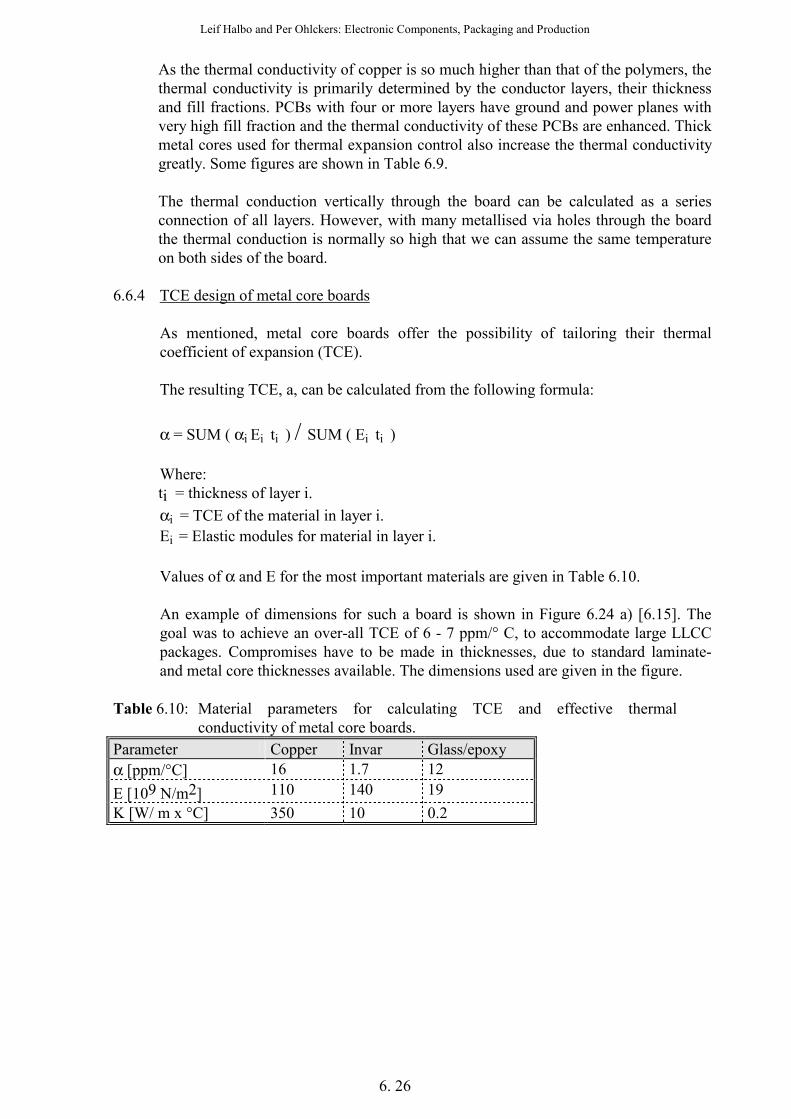
6.6.4 TCE design of metal core boards As mentioned, metal core boards offer the possibility of tailoring their thermal
coefficient of expansion (TCE). The resulting TCE, a, can be calculated from the following formula: α = SUM ( αi Ei ti ) / SUM ( Ei ti ) Where: ti = thickness of layer i. αi = TCE of the material in layer i. Ei = Elastic modules for material in layer i. Values of α and E for the most important materials are given in Table 6.10. An example of dimensions for such a board is shown in Figure 6.24 a) [6.15]. The
goal was to achieve an over-all TCE of 6 - 7 ppm/° C, to accommodate large LLCC packages. Compromises have to be made in thicknesses, due to standard laminate- and metal core thicknesses available. The dimensions used are given in the figure.
Table 6.10: Material parameters for calculating TCE and effective thermal
conductivity of metal core boards. Parameter Copper Invar Glass/epoxy α [ppm/°C] 16 1.7 12 E [109 N/m2] 110 140 19 K [W/ m x °C] 350 10 0.2
Leif Halbo and Per Ohlckers: Electronic Components, Packaging and Production
6. 27
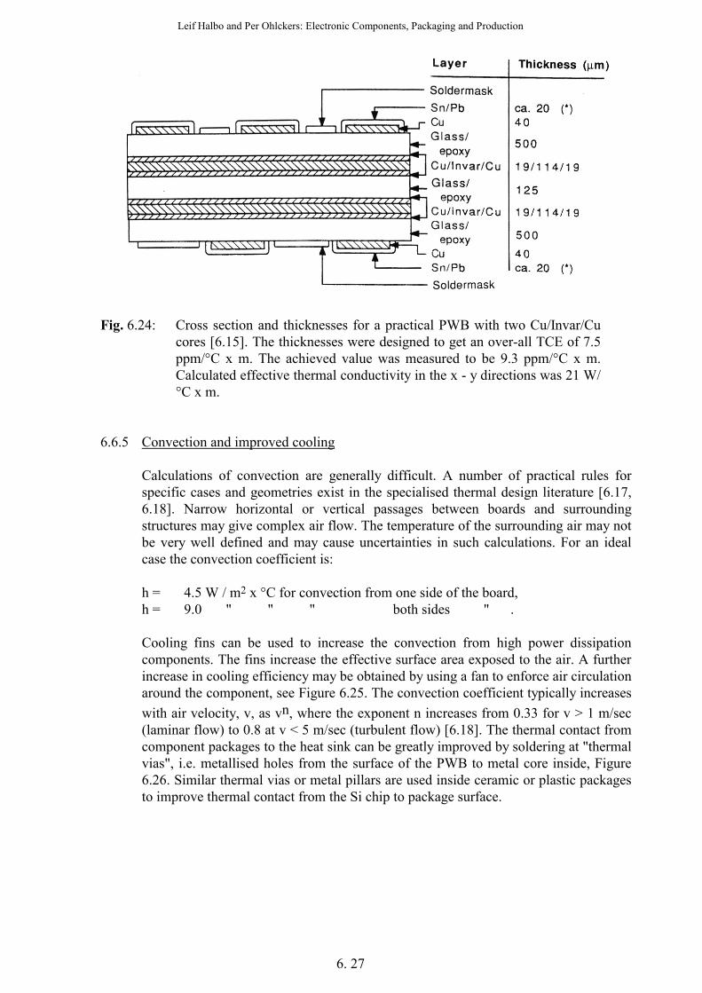
Fig. 6.24: Cross section and thicknesses for a practical PWB with two Cu/Invar/Cu
cores [6.15]. The thicknesses were designed to get an over-all TCE of 7.5 ppm/°C x m. The achieved value was measured to be 9.3 ppm/°C x m. Calculated effective thermal conductivity in the x - y directions was 21 W/ °C x m.
6.6.5 Convection and improved cooling Calculations of convection are generally difficult. A number of practical rules for
specific cases and geometries exist in the specialised thermal design literature [6.17, 6.18]. Narrow horizontal or vertical passages between boards and surrounding structures may give complex air flow. The temperature of the surrounding air may not be very well defined and may cause uncertainties in such calculations. For an ideal case the convection coefficient is:
h = 4.5 W / m2 x °C for convection from one side of the board, h = 9.0 " " " both sides " . Cooling fins can be used to increase the convection from high power dissipation
components. The fins increase the effective surface area exposed to the air. A further increase in cooling efficiency may be obtained by using a fan to enforce air circulation around the component, see Figure 6.25. The convection coefficient typically increases with air velocity, v, as vn, where the exponent n increases from 0.33 for v > 1 m/sec (laminar flow) to 0.8 at v < 5 m/sec (turbulent flow) [6.18]. The thermal contact from component packages to the heat sink can be greatly improved by soldering at "thermal vias", i.e. metallised holes from the surface of the PWB to metal core inside, Figure 6.26. Similar thermal vias or metal pillars are used inside ceramic or plastic packages to improve thermal contact from the Si chip to package surface.

Leif Halbo and Per Ohlckers: Electronic Components, Packaging and Production
6. 28
Fig. 6.25: a): Pin-grid package with cooling fins. b): Measured thermal resistance in
the component with forced air cooling [6.15].

Leif Halbo and Per Ohlckers: Electronic Components, Packaging and Production
6. 29
Fig. 6.26: LLCC package with thermal solder lands and thermal vias connected to a
metal core in the PCB. In power electronic applications the component packages are often attached directly to
a massive metal cooling fin. A layer of thermal grease or other terminally conducting layer is used between the component and the cooling fins to improve the thermal conduction. See also Section 8.6 on power electronic modules.
More sophisticated cooling technologies utilise other media than air. Helium or
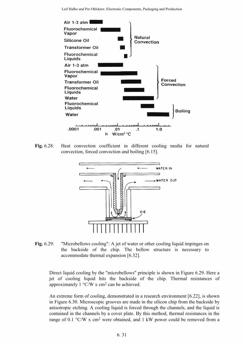
fluorocarbon vapour are gases with better cooling properties than air. Liquids such as water, fluorocarbons and oils are used for cooling the backside or edges of the PCB, see Figure 6.27. Evaporation cooling (boiling) with fluorocarbon liquids is the ultimate cooling technology used in some high end computer applications. The convection coefficient obtained is 3 orders of magnitude larger than for air convection, see Figure 6.28. Fluorocarbon liquids with different boiling temperatures are available. The fluorocarbon may either cool the substrate or be in direct contact with the chip surface. Some issues in this technology such as the effect of contaminations in the liquid and corrosion effects are not fully investigated [6.15- 6.21].

Leif Halbo and Per Ohlckers: Electronic Components, Packaging and Production
6. 30
Fig. 6.27: a): Forced air convection in a channel between two PCBs (Texas
Instruments), b): water-cooled heat exchanger for edge cooling of PCBs and temperature
distribution (qualitative) [6.18].
Leif Halbo and Per Ohlckers: Electronic Components, Packaging and Production
6. 31
Fig. 6.28: Heat convection coefficient in different cooling media for natural convection, forced convection and boiling [6.15].
Fig. 6.29: "Microbellows cooling": A jet of water or other cooling liquid impinges on
the backside of the chip. The bellow structure is necessary to accommodate thermal expansion [6.32].
Direct liquid cooling by the "microbellows" principle is shown in Figure 6.29. Here a
jet of cooling liquid hits the backside of the chip. Thermal resistances of approximately 1 °C/W x cm2 can be achieved.
An extreme form of cooling, demonstrated in a research environment [6.22], is shown
in Figure 6.30. Microscopic grooves are made in the silicon chip from the backside by anisotropic etching. A cooling liquid is forced through the channels, and the liquid is contained in the channels by a cover plate. By this method, thermal resistances in the range of 0.1 °C/W x cm2 were obtained, and 1 kW power could be removed from a

Leif Halbo and Per Ohlckers: Electronic Components, Packaging and Production
6. 32
chip of area 1cm2. Etching the grooves in a passive Si chip and replacing the cover plate with the active chip only gave a slight reduction in the cooling efficiency.
Fig. 6.30: Cooling by forcing liquid through microscopic, etched channels in the
semiconductor chip [6.32]. The channels are approximately 400 µm deep and 100 µm wide.
6.6.6 Thermal simulation and measurement There are many software packages available for numerical simulation of the thermal
behaviour of electronic systems. Some of these programs are general thermal simulation programs, others are specialised for electronics [6.15,6.18]. The general programs usually require more effort from the designer during the input of geometry data and material properties than the specialised programs. However, a general program may offer more design freedom and possibilities for special analysis.
The input data to thermal simulation programs may be divided into three groups:
Geometry data, boundary conditions and material properties. Geometry data are generated by defining points, curves, surfaces and volumes in a thermal CAD system. The geometrical model has to be divided into nodes and elements. This is usually done automatically in modern programs and is otherwise very time consuming.
Boundary conditions are convection coefficients and heat sink/ambient temperatures. Material properties are often contained in a material library in the program. A common source of error in thermal simulation is the use of erroneous input parameters such as an effective convection coefficient or material property. The latter is often due to the fact that bulk material properties are different from the thermal properties of the specially processed materials encountered in electronic packages and substrates. In addition, the interfaces between different materials are difficult to model properly in these programs. Some experimental data and experience are usually required in order to obtain satisfactory results when material interfaces make a significant contribution to the thermal resistance.
Leif Halbo and Per Ohlckers: Electronic Components, Packaging and Production
6. 33
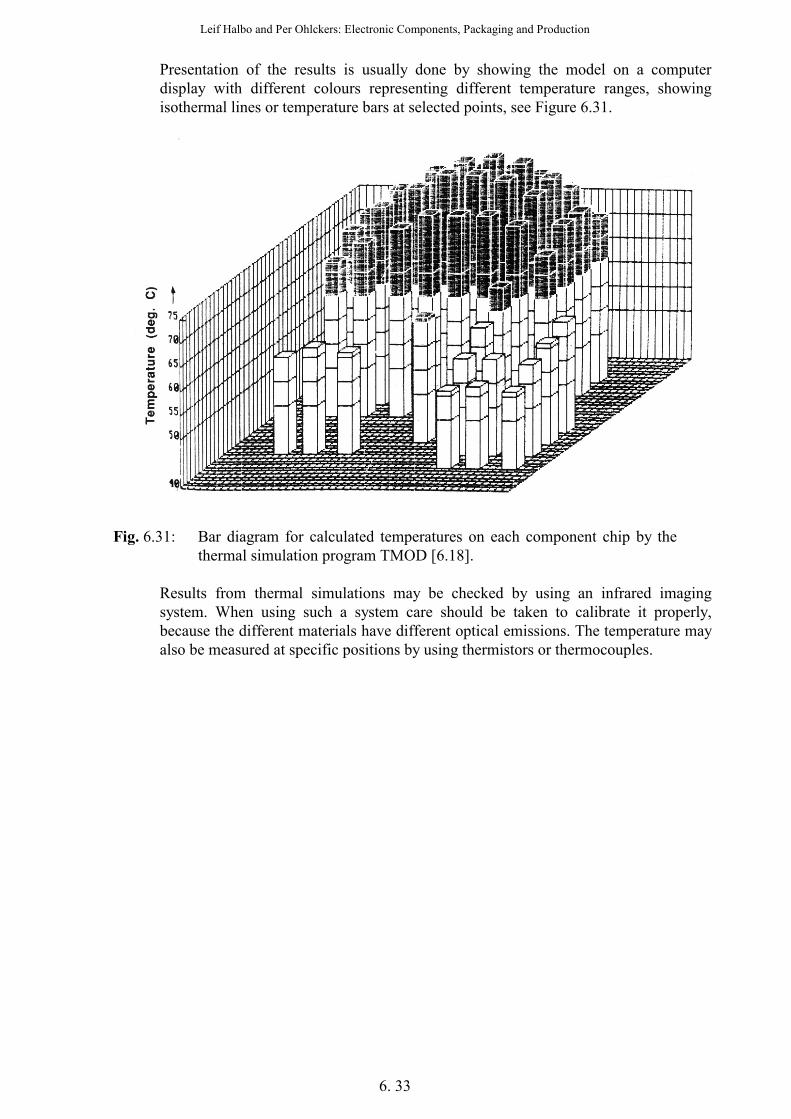
Presentation of the results is usually done by showing the model on a computer display with different colours representing different temperature ranges, showing isothermal lines or temperature bars at selected points, see Figure 6.31.
Fig. 6.31: Bar diagram for calculated temperatures on each component chip by the
thermal simulation program TMOD [6.18]. Results from thermal simulations may be checked by using an infrared imaging
system. When using such a system care should be taken to calibrate it properly, because the different materials have different optical emissions. The temperature may also be measured at specific positions by using thermistors or thermocouples.

Leif Halbo and Per Ohlckers: Electronic Components, Packaging and Production
6. 34
6.6.7 Selection of cooling methods Insufficient cooling of electronic systems leads to problems with low reliability and
reduced lifetime. On the other hand a complicated cooling systems may be very costly. Some cooling methods arranged according to increasing cost and complexity are:
- Use of low power components (CMOS) and design methods. - Optimal placement of high heat dissipating components. - Cooling fins on single components. - Improved thermal properties of the substrate: Metal core board, heat
sinks along edges, change to alumina/thick film module. - Forced air cooling with fan. - Indirect liquid cooling. - Direct liquid cooling with components immersed in the liquid.
More details of thermal design are given in [6.15-6.18]. 6.7 HIGH FREQUENCY DESIGN Transmission line- and other high frequency design principles are gaining increasing
importance due to the increasing speed of integrated circuits. Only a brief summary of the basic principles will be given here due to the size and complexity of this field. Thorough treatments can be found in [6.16, 6.22, and 6.32].
High frequency design should be employed if the cycle time of analogue signals, or
rise time of digital signals, tr, is comparable to tf. Where tf is the time-of-flight delay of a signal over the length l of the critical paths on the board/circuit. As a rule of thumb transmission line phenomena become significant when [6.32]:
tr < 2.5 tf. Eq. 6.1 where tr = 10 - 90 % rise time, and tf = l/v and v is the propagation speed for the signal. The high frequency design methods are based on calculation of the electromagnetic
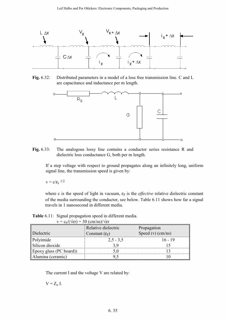
field in the vicinity of the electrical conductors, solving the "Telegrapher's equation" [6.32]. The conductors are modelled by distributed electrical inductance, capacitance and resistance, see Figures. 6.32 - 6.33. The distributed electrical parameters depend on the geometry of the conductor and its position relative to ground and power planes, besides the materials used.
Leif Halbo and Per Ohlckers: Electronic Components, Packaging and Production
6. 35
Fig. 6.32: Distributed parameters in a model of a loss free transmission line. C and L
are capacitance and inductance per m length.
Fig. 6.33: The analogous lossy line contains a conductor series resistance R and
dielectric loss conductance G, both per m length. If a step voltage with respect to ground propagates along an infinitely long, uniform
signal line, the transmission speed is given by: v = c/εr 1/2 where c is the speed of light in vacuum, εr is the effective relative dielectric constant
of the media surrounding the conductor, see below. Table 6.11 shows how far a signal travels in 1 nanosecond in different media.
Table 6.11: Signal propagation speed in different media. v = c0/(√εr) = 30 (cm/ns)/√εr Dielectric
Relative dielectric Constant (εr)
Propagation Speed (v) (cm/ns)
Polyimide 2,5 - 3,5 16 - 19 Silicon dioxide 3,9 15 Epoxy glass (PC board)) 5,0 13 Alumina (ceramic) 9,5 10 The current I and the voltage V are related by: V = Zo I.
Leif Halbo and Per Ohlckers: Electronic Components, Packaging and Production
6. 36
The fundamental quantity Zo is the characteristic impedance: Zo = ((R + jωL)/(G + jωC))1/2 where: ω = angular frequency R = resistance of the conductor per unit length L = inductance per unit length C = capacitance per unit length G = loss conductance in dielectric per unit length. In a loss free medium: Zo = L/C . An electrical signal travelling through a discontinuity between media 1 and 2 is
reflected with a coefficient of reflection given as: R = (Z1 - Z2)/(Z1 + Z2) where Z1 and Z2 are the characteristic impedances in the two media. When the
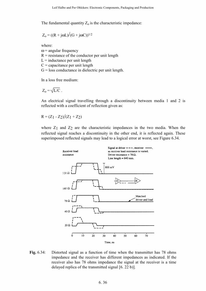
reflected signal reaches a discontinuity in the other end, it is reflected again. These superimposed reflected signals may lead to a logical error at worst, see Figure 6.34.
Fig. 6.34: Distorted signal as a function of time when the transmitter has 78 ohms
impedance and the receiver has different impedances as indicated. If the receiver also has 78 ohms impedance the signal at the receiver is a time delayed replica of the transmitted signal [6. 22 b)].

Leif Halbo and Per Ohlckers: Electronic Components, Packaging and Production
6. 37
An electrical conductor should be treated as a transmission line if the condition of Eq.
6.1 applies. On PCBs this is typically the case for clock frequencies above 50-100 MHz. It also depends on conductor lengths and materials. The effects may have to be considered in circuits operating at lower clock frequencies for fast ICs with steep pulse flanks. At even higher frequencies also sharp bends on cables, and via holes, may affect the transmission of signals.
An un-terminated conductor should normally be terminated by a resistor with the
same resistance as the characteristic impedance and as close as possible to the end of the conductor.
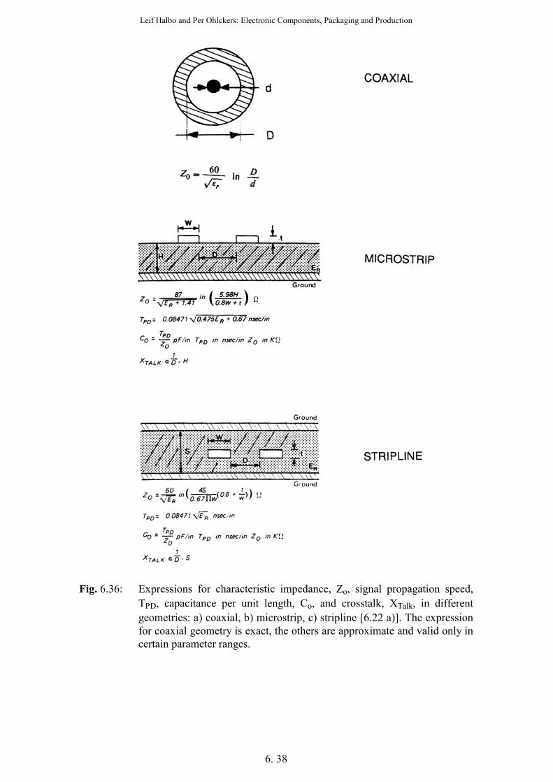
Common geometries for transmission lines are cylindrical and rectangular coaxial
structures, coplanar, microstrip, stripline, and derived structures, see Figure 6.35. In all the geometries, one or two ground plane(s) will be located close to the signal conductor in order to confine the electrical field. Capacitance and inductance are related to geometrical dimensions and material properties in a complex manner for most geometries. The effective relative dielectric constant is determined by the dielectric underneath the conductor as well as the air, in case of microstrip geometry. Usually numerical calculations are necessary to calculate the Zo but some approximate analytical results are available, see Figure 6.36 and [6.22 - 6.23]. The relationship between Zo and other parameters is shown in Figure 6.37. Zo may also be frequency- and temperature dependent due to temperature dependence of the dielectric properties, please refer to Figure 5.14. In a production environment tolerances in Zo must be considered, due to limited standard values in thicknesses, and tolerances in linewidths, thicknesses, dielectric constant, etc.
Fig. 6.35: Geometries for obtaining a controlled characteristic impedance. The typical configuration in a multilayer PCB or hybrid module is microstrip outer
signal layer and buried microstrip or stripline inner layers with possibilities of using two signal layers between a set of ground planes. Standard values, most often used for characteristic impedance, are 50, 75 and 95 ohms.
Leif Halbo and Per Ohlckers: Electronic Components, Packaging and Production
6. 38
Fig. 6.36: Expressions for characteristic impedance, Zo, signal propagation speed,
TPD, capacitance per unit length, Co, and crosstalk, XTalk, in different geometries: a) coaxial, b) microstrip, c) stripline [6.22 a)]. The expression for coaxial geometry is exact, the others are approximate and valid only in certain parameter ranges.

Leif Halbo and Per Ohlckers: Electronic Components, Packaging and Production
6. 39
Fig. 6.37: Dependence of the characteristic impedance on geometric dimensions, for
a) stripline and b) microstrip. w is the signal conductor width, S is the distance between ground planes for stripline, and H the distance between signal conductor and ground plane for microstrip (please refer to Figure 6.35). Curves are shown for different signal conductor thicknesses, t [6.9].

Leif Halbo and Per Ohlckers: Electronic Components, Packaging and Production
6. 40
Fig. 6.38: Cross talk: A signal from A to C is transmitted to the B - D line and gives
noise in B (backward or near end cross talk) and in D (forward or far end cross talk).
Small spatial separation between conductors results in capacitive and inductive coupling between the conductors and potential problems with cross talk, see Figure 6.38. Cross talk is the main consideration when defining minimal line separation for high frequency circuits. Forward cross talk is propagated in the same direction as the source signal and backward cross talk in the opposite direction, Figure 6.39 [6.16, 6.22 b]. Cross talk and reflections are different types of noise.
Fig. 6.39: Backward cross talk as a function of conductor separation in stripline
geometry in different dielectrics. The effect increases with increasing εr and decreases with increasing conductor separation [6.24].

Leif Halbo and Per Ohlckers: Electronic Components, Packaging and Production
6. 41
A third kind is switching noise. If the electrical current in a component is suddenly
changed there will appear a transient signal on the power supply line due to the inductance in it. This type of noise may also lead to logical errors or delays [6.16]. It is important to ensure a high electrical conductivity in ground planes and power supply conductors [6.16, 6.33]. Decoupling capacitors between ground and power supply close to critical components are also important, to absorb current spikes without corresponding voltage spikes.
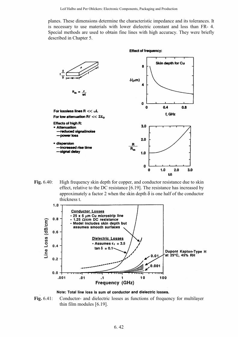
Losses also have to be considered. The losses may be described by the attenuation of
the signals [6.16]. The signal attenuation between points a and b, separated by a distance l of the conductor, is given as:
Vb = Va exp(-αl) where α is the attenuation coefficient. The attenuation is related to ohmic-, skin- and dielectric losses (with attenuation
coefficients αr, αs, αd respectively). α = (αr, αs ) + αd . In the parenthesis αr dominates at low frequencies. αs dominates at very high
frequencies (GHz) where the skin depth ds is much smaller than the conductor cross section. Simplified expressions for each parameter are [6.32]:
αr = R / (2Zo) αs = (π µo f ρ)1/2 / (w Zo) for δs = (ρ / π f µo)1/2 << t αd = π (εoε)1/2 f tan δ / c where: R = ohmic resistance per unit length, ρ = electrical DC resistivity in the conductor, tan δ = dielectric loss tangent (please refer to Section 3.2.3), w =conductor width, and t = conductor thickness. c = speed of light (3·108 m/s) An increased rise time for a step signal is also among the consequences of lossy lines,
because the high frequency signal components are attenuated more than the low frequency components, as shown in the expressions for αd and αs. Figure 6.40 shows the skin effect in copper conductors and Figure 6.41 shows a comparison between conductor- and dielectric losses in multilayer thin film multichip modules (MCMs).
High frequency design of PCBs and hybrid modules presents new demands on
designers and manufacturers. The layout of the PWB must be properly controlled. CAD software for high frequency design is still in its infancy. Materials and dimensions must be selected and controlled in close co-operation with the manufacturer.
Manufacturing of high frequency PCBs gives tough demands on tolerances for
conductor width and thickness of dielectric layers between conductors and ground
Leif Halbo and Per Ohlckers: Electronic Components, Packaging and Production
6. 42
planes. These dimensions determine the characteristic impedance and its tolerances. It is necessary to use materials with lower dielectric constant and loss than FR- 4. Special methods are used to obtain fine lines with high accuracy. They were briefly described in Chapter 5.
Fig. 6.40: High frequency skin depth for copper, and conductor resistance due to skin
effect, relative to the DC resistance [6.19]. The resistance has increased by approximately a factor 2 when the skin depth δ is one half of the conductor thickness t.
Fig. 6.41: Conductor- and dielectric losses as functions of frequency for multilayer
thin film modules [6.19].

Leif Halbo and Per Ohlckers: Electronic Components, Packaging and Production
6. 43
6.8 DESIGN OF FLEXIBLE PRINTED CIRCUITS As mentioned in Section 5.12 the primary applications of flexible printed circuits are
compact packaging in 3 dimensions, interconnection to moving parts, advanced flat cables, membrane switch panels. Design of regular flex boards is discussed below, membrane switch panels are described in Section 6.9.
The base material for flex boards is normally polyimide. Polyester may also be used if
soldering can be avoided. These materials were briefly discussed in Section 3.3, and some data for the base materials were shown in Table 5.4.
Direct conversion of rigid PCBs to flex boards is usually not an optimal design
procedure. The 3-dimensional aspect should be considered from the beginning of the design. Simple models cut from a piece of paper may be helpful for visualisation of the shape.
The flexible materials will typically shrink 0.2 % during processing compared to 0.05
% for FR-4. This has to be considered during the design work. Determination of minimum dimensions of conductors with large current loads was
shown in Figure 6.2 for ordinary PWBs and is also valid for flexible PCBs (flex prints). The adhesion between copper foil and base material is not so good as than for rigid PCBs and is further reduced for conductor widths below 0.5 mm. Generally, as wide conductors as possible should be used in order to ensure the best possible stability and production yield.
Sharp bends will reduce the reliability due to fatigue in the copper, Figure 6.42. The
minimum bending radius depends on whether the flex print will be bent only once during installation (e.g. electronics of a compact camera) or if the bends are dynamic (such as the writing head of a typewriter or in a computer printer. If possible, only one conductor layer should be used in the bending zone and the copper layer should be in the middle of the flex print. In a multilayer flex print the copper layers should not be directly on top of each other in the bending zone [6.25-6.26]. Conductors should be oriented perpendicularly to the bend.
The flex print is shaped by cutting with a numerically controlled knife or with
excising, depending on production volumes. Sharp corners on the copper foil or base material may lead to tearing of the foil and should be avoided, Figure 6.43.
If through hole mounted components are attached to flex prints then a rigid material
should be used beneath the component to increase strength and solderability. Such rigid sections are also used for other purposes. They may simply be pieces of rigid plastic sheets or single- or multilayer boards. The flexible parts may be simple interconnection parts or they may be complete wiring boards. Components should not be attached to the moving parts of a flex print.

Leif Halbo and Per Ohlckers: Electronic Components, Packaging and Production
6. 44
Fig. 6.42: Bending of double layer flexible print with different conductor layout. The
Figure shows the number of cycles before failure with 5, 10 and 20 mm bending radius and 180° angel of bending. (Data: Schoeller Elektronik). If the copper layer in the bending zone is strained 16 % or more it is likely to fail during the first cycle.
Fig. 6.43: a): Solder lands on flexible prints should be rounded in order to reduce the
possibility for failures, b): The contour of the board should be rounded in order to reduce possibilities for tearing (dimensions in inches). The "rabbit ears" on the ends of the metal foil is for obtaining better adhesion to the polyimide. c): Plastic rivets should be used to avoid sharp bends in the interface between the flexible and the rigid parts of the PCB.

Leif Halbo and Per Ohlckers: Electronic Components, Packaging and Production
6. 45
The polyimide flex prints can be soldered by wave-, reflow- or hand soldering.
Soldering and positioning of components usually require special tooling that must be considered during the design work.
Interconnection of flex prints is done by spring loaded mechanical connectors,
soldering or use of conductive adhesives. Vibration testing is often important because the flex prints are usually free to move
during operation. Flex prints typically have a 2 - 3 times higher cost than comparable rigid PCBs. More details regarding applications, design and fabrication are given in [6.3 and 6.25 -
6.28]. 6.9 DESIGN OF MEMBRANE SWITCH PANELS [6.31] A printed keyboard or membrane switch panel (please refer to Section 5.12) is a part
of the interface between the electronic equipment and the user. The main electrical function is switching, but it may also include an LCD display or light emitting diodes (LED's) for information to the user. Design and production of these panels is a speciality and there should be a close co-operation between the designer and the manufacturer.
It is important to define user specifications such as: indoor/outdoor use, minimum and
maximum operating temperatures, reliability requirement, atmospheric conditions, etc. These specifications influence the selection of materials and design rules. If displays, back lighting (Figures 6.44, 6.45), windows, etc. are needed then this should be considered from the beginning of the design.
The standard parts of a membrane switch panel were shown in Figure 5.21, and a
more complex type is shown in Figure 6.44. The panel is attached to the front panel of the equipment with an adhesive bottom foil. The top layer includes informative text and graphical information made by screen printing. The two electrically active layers are made by screen printing of electrical conductors and contact pads with a silver based polymer thick film technique (see Section 8.3). The electrical layers are separated with spacers. Normally, such a switch panel will endure some 5 million activation's of any switch. If metal domes are used for the switches the expected lifetime will typically be 1-2 million activation's [6.31].

Leif Halbo and Per Ohlckers: Electronic Components, Packaging and Production
6. 46
Fig. 6.44: Detail of a membrane switch panel. The tail with interconnections to the
panel is protected with a laminated foil. Light emitting diodes may be attached with conductive adhesive. Screen printed polymer thick film series resistors may be used [6.31].
Fig. 6.45: Contact areas of membrane switch panel with back lighting and window.
Examples of lighted text on a dark background and the opposite combination. If a metal dome is used the information has to be next to the key and not underneath it [6.31].

Leif Halbo and Per Ohlckers: Electronic Components, Packaging and Production
6. 47
If necessary, several layers of electrical conductors may be printed on top of each other with electrical insulation in between (Section 8.3).
The most common cause of failure is mishandling. Short circuits due to silver
migration [6.31] may also occur if humidity is penetrating into the switch panel. The panel itself is well protected by many protective layers outside the electrically active layers. However, the "tail" or connector between the panel and the outside world, see Figure 6.44, is a weak point.
LED's may be included in the keys for information purposes. The LED's are attached
with conductive adhesive because the polyester material will not withstand the temperatures of a soldering process.
Further details of membranes with panel technology and design are given in [6.31]. 6.10 SYSTEM LEVEL MODELLING In the early phase of the development of a complex electronic product the emphasis is
on over-all specifications and performance of the system, division into suitable subsystems and choice of packaging technology for each subsystem. Computer models have been developed to simulate the whole system, with the freedom to test out various technologies for each subsystem and change the content in each subsystem. We shall only briefly mention one such model, SUSPENS [6.32]. Each IC technology is defined by parameters describing delay, minimum dimensions, line resistance and capacitance, power per gate, etc. Chip architecture is also characterised. Based on the number of logic gates per chip the no. of I/Os and the average interconnection length are calculated via Rent's rule. The chip size can be calculated, as well as maximum clock frequency, power consumption, etc. Module- and board technologies, likewise, are defined by their characteristic parameters.
In this way a hierarchical model is built. "What if "- questions can be tested by
changing an important technology parameter (e.g. CMOS minimum line width) changing technology for a block in the model (e.g. replace thick film hybrid technology by thin film MCM technology), etc. The consequence for the over-all system performance can be analysed by comparing for various conditions such parameters as maximum system clock frequency, computational capacity, packing density, power dissipation density and over-all power dissipation, cost indicators, etc. Figure 6.46 shows the SUSPENS model schematically. This kind of system simulation is expected to gain increasing importance.

Leif Halbo and Per Ohlckers: Electronic Components, Packaging and Production
6. 48
Fig. 6.46: The SUSPENS model for the different levels in an electronic system. The
symbols are parameters characterising the system and different technologies of the system. They are quantified and used to compare or optimise different possible versions of the system in computer calculations [6.32].
REFERENCES [6.0] Among the large number of EMC standards we shall just mention: a) CISCR, Publication 22: "Limits and methods of measurements of radio
interference characteristics of information technology equipment". The European norm EN 55022 is based on this standard. They cover emission.
b) IEC Publication 801 - 1 to - 5, as well as EN 55020: "Immunity from radio interference of broadcast receivers and associated equipment" cover immunity.
c) EEC Directive KOM (87) 527 and KOM (88) 548 final (2) cover both emission as immunity.
d) CENELEC TC 110 is responsible for further standards. e) Some principles of EMC design are described in P. Krebs and H. G. Nissen:
"EMC handbook part 3: EMC considerations in PWB layout". Technical report, ElectronikCentralen ECR-224, 1989 (in Danish).
[6.1] G. Leonida: "Handbook of printed circuit design, manufacture, components and
assembly". (Electrochemical Publications, 1981.)

Leif Halbo and Per Ohlckers: Electronic Components, Packaging and Production
6. 49
[6.2] C. Lea: "A scientific guide to surface mount technology". (Electrochemical Publications, 1988.)
[6.3] C. F. Coombs: "Printed circuits handbook". (3rd Ed., McGraw Hill, 1988.) [6.4] ANSI/IPC-SM-782: "Surface Mount Land Patterns". (IPC, March 1987.) [6.5] L. Halbo m. fl.: "Handbook for design and production of surface mounted
PCBs". (ABB Handbook, 1986, in Norwegian.) [6.6] "SMD-Technology: Guidelines for Footprint Design". (Philips Components,
1989.) [6.7] "An Introduction to Surface Mounting", and "PCB Layout Recommendations".
(Siemens, 1986.) [6.8] S. Hinch: "Handbook of Surface Mount Technology". (Longman, 1988.) [6.9] C. G. Bergendahl og H. Svard: "SMT Handbook, Chapter 3: Design". (IVF-
report 87606, Sveriges Mekanforbund 1987, in Swedish.) [6.10] "Tape Automated Bonding at EM Marin". Design rules, 1987. [6.11] L. Halbo m. fl.: "Second Generation SMT". EPF-report R 29, 1989. (In
Norwegian.) [6.12] A. Gabrielsen m. fl.: "In-circuit test of SMT PCBs". EKF-report R 60, December
1987. (In Norwegian.) [6.13] J. Wangensteen: "SMT testing". EKF-report R 43, March 1986. (In Norwegian.) [6.14] a): G. Stensjø: "SMT Handbook Chapter 5: Control and testing." (IVF-report
87620, 1987. In Swedish.) b): COMETT INSIGHT course: "Modern Trends in Digital Testing". J.
McClean, Heriot-Watt University 1993. [6.15] L. Halbo et al.: a): "Termal design of PCBs". EKF-report R 42, 1986. b):
"Environmental tests on surface mount PCBs of different structures". EPF-report R 19, 1987. (In Norwegian.)
[6.16] R. Tummala and E. J. Rymaszewski: "Microelectronics Packaging Handbook".
(Van Nostrand, 1989.) [6.17] a): G. Ellison: "Thermal computations for Electronic Equipment". (van
Nostrand, 1984.) b): A. D. Krauss and A. Bar-Cohen: "Thermal analysis and Control of Electronic
Equipment". (McGraw-Hill, 1983.) c): D. J. Dean: "Thermal Design of Electronic Circuit Boards and Packages".
(Electrochemical Publications, 1985.) d): F. Rasmussen et al.: "Thermal design", EKF-report R 69, 1989. (In
Norwegian.)

Leif Halbo and Per Ohlckers: Electronic Components, Packaging and Production
6. 50
e): L. Jensen et al.: "Thermal conduction in electronics". EKF-report R 55, 1988. (In Norwegian.)
[6.18] a): G. Floodman and A. Sihlbom: "Handbook for thermal design". IVF-report
88822, 1989. (In Swedish.) b): A. Sihlbom og H. Svard: "Mätteknik for measuremen of temperature in
electronics". IVF-report 87615, 1987. (In Swedish.) [6.19] R. Jensen: "Materials and Processes for Thin Film Multilayer Multichip
Packaging". Presented in CEI-Europe Elsevier "Course on Advanced Semiconductor Packaging", Garmish, November 1988.
[6.20] T. Dewey: "Developments in Liquid immersion Cooling". Electronics Packaging
and Production, April 1988, p. 59. [6.21] P. Øhlckers: "Thermal design". Technical report, 1989. (In Norwegian.) [6.22] a): G. Ginsberg: "Surface Mount and Related Technologies". (Marcel Dekker,
1989.) b): D. R. Seraphim et al.: "Principles of Electronic Packaging". (McGraw-Hill,
1989.) c): T. Gleditsch et al.: "Design of high frequency PCBs, a handbook." EPF-
report R-38, March 1990. (In Norwegian.) [6.23] H. Svärd and A. Sihlbom: "High frequency electrical design". IVF-report 88622,
1988. (In Swedish.) [6.24] D. J. Arthur: "Electrical and Mechanical Characteristics of Low Dielectric Constant PCBs". Proc. IPC Conference, Boston 1986, 0179-027-1.0C. [6.25] S. Gurley: "Flexible Circuits". (Marcel Dekker, 1984.) [6.26] J. J. Miniet: "End User´s Guide to Innovative Flexible Circuit Packaging". (Marcel Dekker, 1986.) [6.27] W. S. Rigling: "Rigid-Flex Printed Wiring Design for Production Readyness".
(Marcel Dekker, 1988.) [6.28] ANSI/IPC-D-249: "Design Standard for Flexible Single- and Double-Sided
Printed Boards". (January 1987.) [6.29] Mil. Std. 2118: "Flexible and Rigid-Flex Printed Wiring for Electronic
Equipment". [6.30] J. C. Fjelstad: "Design guidelines for Flexible Circuits". Electronic Packaging &
Production August 1988, p.32. [6.31] L. Halbo (Ed.): "Polymer Thick-Film Technology (PTF) - Design Guidelines
and Applications". (Lobo 1990.)

Leif Halbo and Per Ohlckers: Electronic Components, Packaging and Production
6. 51
[6.32] H. B. Bakoglu: "Circuits, Interconnections and Packaging for VLSI". (Addison Wesley 1990.)
[6.33] O. Pedersen et al.: "Modelling of Power and Ground Planes". Circuit World,
Vol. 18, no.3, 1992, p. 30. [6.34] H. Hamano, Toshiba, private communication. [6.35] R. J. Klein Wassink: "Foot prints of fine-pitch SMDs". Philips report SAQ-
p238, May 1991. [6.36] P. Melville: "Thermal resistance of SO and PLCC packages". Electronic
Components and Applications, vol. 7, no. 4, 1986.