Embed Size (px)
Citation preview
102
CHAPTER 5
DESIGN PROCEDURE AND ANALYSIS OF EMI FILTER
EMI filter is a significant part of SPC to minimize the CM and DM
Conducted emissions in terms of size and cost. This chapter proposes an
advanced and easiest method of EMI filter design for SPC. The practical
approach of measuring the power converter noise spectrum to calculate the
maximum and minimum magnitude of the DM and CM noise source
impedances is proposed. The design of EMI filter is based on the noise source
impedance values. The practical filters like DM choke with X capacitor on
EUT side filter, DM choke with X capacitor on LISN side filter, filter,
complete EMI filter and X2Y filters are investigated.
5.1 INTRODUCTION
The power converters are unable to meet the FCC standards for
Conducted EMI. Accordingly, EMI filters for both CM and DM are added at
the input of the power converters so as to filter out the switching noise and
reduce EMI of other equipments. Mismatch between the EMI source
impedance and the EMI filter output impedance causes poor noise attenuation.
Hence, an easy and efficient EMI filter design technique is essential. In
addition, as the existing EMI filter design techniques do not take into account
the noise source impedance of the SPC, the optimum levels of filtering could
not be achieved.
103
The considered method is simple to understand and does not require
the phase information of the noise source impedance. Hardware results show
that the proposed method is an efficient technique to design EMI filters for
AC-DC half-bridge converter. Passive filters have several significant benefits
in certain applications, because they use no active elements. Passive filters
range is enhanced to large signals where active devices are frequently
impossible.
The EMI filter topology and elements are decided under the
maximum or minimum value of the CM and DM noise source impedances
which provide the smallest attenuation. The input filter on a SPC has two
major purposes: (i) to prevent EMI produced in SPC and its effect on the other
equipment, (ii) to avoid high frequency voltage from power line passing
through the output of the SPC.
5.2 DESIGN OF CM FILTER
The following are required to know the purpose of designing the CM
filter: (i) the attenuation needed to construct the CM noise range above the
EMI standards at the required frequency range and (ii) the minimum noise
source impedance or maximum noise source impedance for the frequency
range of interest.
A passive LC filter result attains both the filtering requirements. The
objective of the input filter design is to achieve the best balance between filter
performance against size and cost. The input filter does not adjust the
converter loop gain, if the output impedance is below the input impedance of
the converter. To avoid oscillation, it is essential to keep the peak output
impedance of the filter must be lower than the input impedance of the
converter.
104
5.2.1 Design Procedure of CM Filter
Procedure for designing CM filter is given below:
STEP 1: CM and DM noise separation using a noise separator.
STEP 2: Using a simple test CM filter, measure the CM noise spectrum
with and without filter.
STEP 3: Calculate the required attenuation along with definite regulations.
STEP 4: Calculate the maximum and minimum values of CM noise source
impedances for the frequency range of interest.
STEP 5: Design the CM filter using maximum or minimum value of the
noise source impedance which provides the least attenuation.
STEP 6: Calculate the spot frequency of the designed CM filter.
STEP 7: Calculate the attenuation of the designed CM filter and if it is
satisfactory, CM filter design is completed.
STEP 8: If spot frequency of the designed CM filter is lesser, go to step 6.
STEP 9: If the designed filter does not meet the required attenuation, then a
suitable filter topology is to be chosen and proceed from step 5.
STEP 10: Test the completed CM filter.
5.2.2 CM Filter Topology
CM filter consists of CM inductor and CY or X capacitor. Regarding
filter topology two cases are considered. When the CM inductor faces the
105
input side of SPC, ZsCM max is used to find CM filter parameters. If X capacitor
faces the input side of SPC, then ZsCM min should be used to select the filter
components.
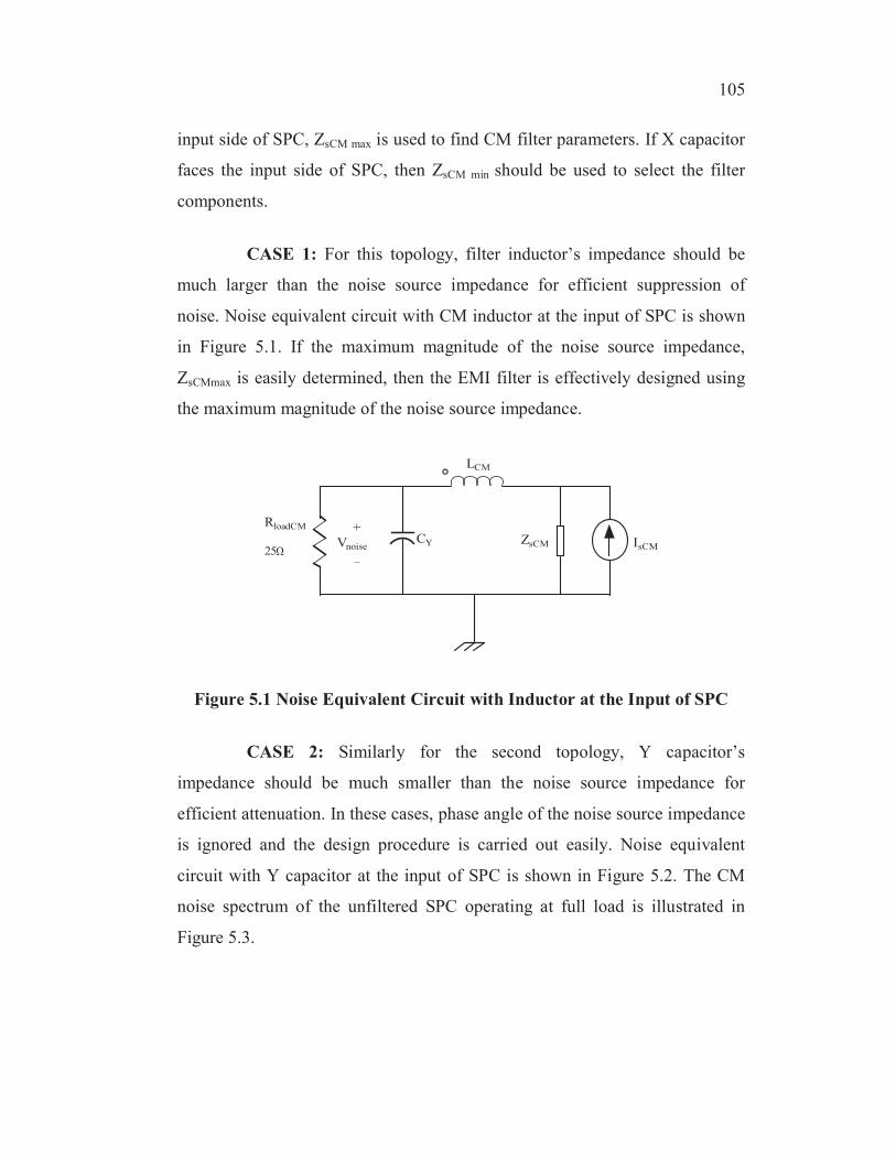
CASE 1: For this topology, filter inductor’s impedance should be
much larger than the noise source impedance for efficient suppression of
noise. Noise equivalent circuit with CM inductor at the input of SPC is shown
in Figure 5.1. If the maximum magnitude of the noise source impedance,
ZsCMmax is easily determined, then the EMI filter is effectively designed using
the maximum magnitude of the noise source impedance.
RloadCM
25CY
+
Vnoise
_
°LCM
ZsCM IsCM
Figure 5.1 Noise Equivalent Circuit with Inductor at the Input of SPC
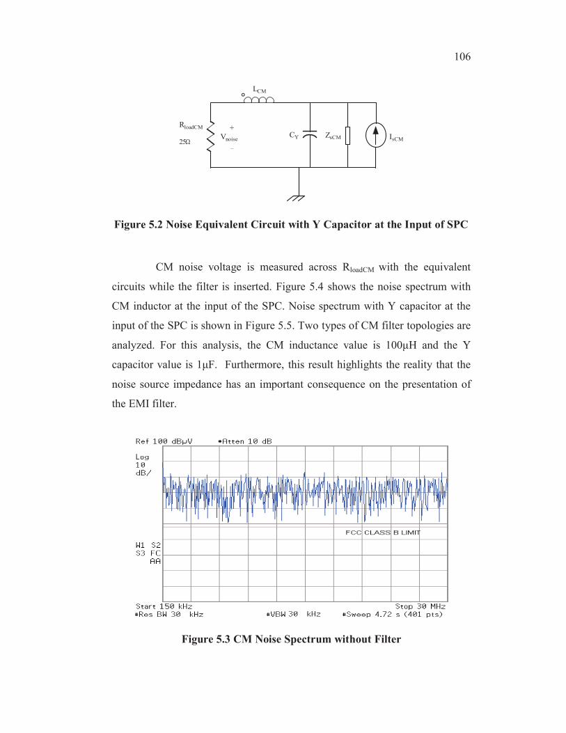
CASE 2: Similarly for the second topology, Y capacitor’s
impedance should be much smaller than the noise source impedance for
efficient attenuation. In these cases, phase angle of the noise source impedance
is ignored and the design procedure is carried out easily. Noise equivalent
circuit with Y capacitor at the input of SPC is shown in Figure 5.2. The CM
noise spectrum of the unfiltered SPC operating at full load is illustrated in
Figure 5.3.
106
RloadCM
25CY
+
Vnoise
_
°LCM
ZsCM IsCM
Figure 5.2 Noise Equivalent Circuit with Y Capacitor at the Input of SPC
CM noise voltage is measured across RloadCM with the equivalent
circuits while the filter is inserted. Figure 5.4 shows the noise spectrum with
CM inductor at the input of the SPC. Noise spectrum with Y capacitor at the
input of the SPC is shown in Figure 5.5. Two types of CM filter topologies are
analyzed. For this analysis, the CM inductance value is 100 H and the Y
capacitor value is 1 F. Furthermore, this result highlights the reality that the
noise source impedance has an important consequence on the presentation of
the EMI filter.
Figure 5.3 CM Noise Spectrum without Filter

107
Figure 5.4 Noise Spectrum of CM Inductor at the Input of the SPC
Figure 5.5 Noise Spectrum of Y Capacitor at the Input of the SPC

108
Table 5.1 CM Noise Voltages
Topology Noise Voltage
Without CM filter 54 dBµV
With CM inductor at the input of the SPC 30 dBµV
With Y capacitor at the input of the SPC 34 dBµV
With the experimental setup, the noise voltage values obtained at 0.5
MHz are tabulated in Table 5.1. From the results, it is concluded that the CM
inductor at the input of the SPC topology should be used because it provides
more attenuation at high frequencies than the X capacitor at the input of the
SPC topology.
5.2.3 SELECTION OF CM FILTER COMPONENTS
The required lowest spot frequency for CM filter is determined
using Equation (5.1).
os
TCMreq
Ff
A (5.1)
fs is the spot frequency of the CM filter and ATCMreq is the required
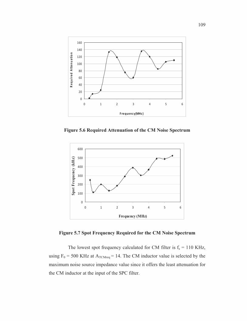
attenuation at frequency F0. The CM attenuation required for the SPC to pass
the FCC Class B standards is plotted as shown in Figure 5.6. Spot frequency
value is calculated at each point for the value obtained from Figure 5.6 using
Equation (5.1). The spot frequency required for the CM noise spectrum to pass
FCC Class B standards is shown in Figure 5.7.
109
0
20
40
60
80
100
120
140
160
0 1 2 3 4 5 6
F re quenc y(MHz )
Re
qu
ire
d A
tte
nu
ati
on
Figure 5.6 Required Attenuation of the CM Noise Spectrum
0
100
200
300
400
500
600
0 1 2 3 4 5 6
Frequency (MHz)
Sp
ot
Fr
equ
en
cy
(k
Hz
)
Figure 5.7 Spot Frequency Required for the CM Noise Spectrum
The lowest spot frequency calculated for CM filter is fs = 110 KHz,
using F0 = 500 KHz at ATCMreq = 14. The CM inductor value is selected by the
maximum noise source impedance value since it offers the least attenuation for
the CM inductor at the input of the SPC filter.
110
The noise voltage without CM filter at 0.5 MHz is measured to be 54
dBµV as shown in Figure 5.3 and with CM test filter is 30 dBµV as shown in
Figure 5.4. With these values, attenuation is found to be 15.85. From Equation
(4.16), the maximum value of ZsCM is found to be 168 by series insertion
method. With the experimental setup, the noise source impedance values
obtained at 0.5MHz are tabulated in Table 5.2.
Table 5.2 CM Noise Source Impedance Value
Attenuation CM Noise Source Impedance
Maximum value
15.85 168
CM inductor impedance ZLCM must be twice the maximum CM noise
source voltage.
ZLCM >> 2 × |ZsCM|Max
>> 2 × 168
>> 336
CM inductor impedance value must be greater than 336 . From
this value LCM is calculated as 106.9 µH. The inductance selected is any
practical value above 106.9 µH. In order to leave some margin, a 110 µH
inductor is selected. The impedance of this CM inductor at 500 KHz is 346
which is greater than two times the maximum value of the CM noise source
impedance.
111
Considering the CM noise source impedance as purely resistive, the
attenuation of the topology in Figure 5.1 is stated by Equation (5.2) where V1
and V2 are known by Equations (5.3) and (5.4), respectively. Factors Z1 and Z2
are provided by Equations (5.5) and (5.6), respectively
2TCM
1
VA =
V (5.2)
where,
1 21 sCM
LCM 1
Z ZV = I
(Z + Z ) (5.3)
load sCM2 sCM
load sCM
R ZV = I
R + Z (5.4)
load CY1
load C Y
R ZZ =
R + Z (5.5)
sCM2 LCM 1
sCM 1 LCM
ZZ = (Z + Z )
Z + Z + Z (5.6)
ZLCM is the impedance of the CM inductor. ZCY is the impedance of
the Y capacitor. V2 is the voltage across the LISN equivalent resistor shown in
Figure 5.1 and V1 is the noise voltage across the LISN resistor without the CM
filter. The final step in the filter design is to select the capacitance. A
capacitance of 94 nF is selected using two CY capacitors of 47nF each in
parallel. Using this capacitance and Equation (5.2), the calculated attenuation
of the filter at 500 KHz is 15.45 which is greater than the required attenuation
14. Experimental waveform obtained after placing the designed CM filter is
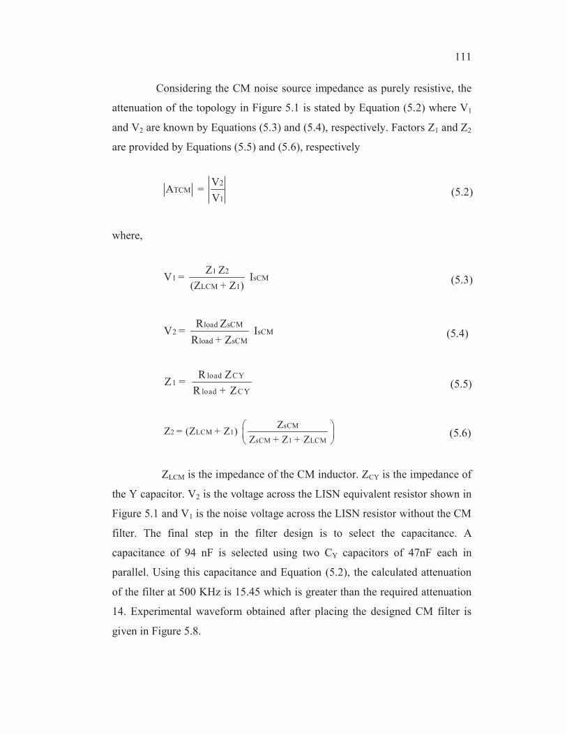
given in Figure 5.8.
112
Figure 5.8 CM Noise Spectrum after the Designed CM Filter
The SPC with CM filter passed the FCC 15 Class B requirements
over the required frequency range and the attenuation achieved is greater than
the 3-dB margin over most of the frequency range.
If the capacitance is selected based on an ideal LC filter design, the
calculated capacitance required would be 21nF using Equation (5.7). The
closest available capacitance is 22 nF.
0C
CM Y
Ff =
2 L C (5.7)
Using Equation (5.2) with the parameters CY = 22nF, RloadCM = 25 ,
LCM = 100µH, and ZSCM = 132 , the calculated attenuation is 7.9 at 500 KHz
which is less than the required attenuation, ATreqCM = 14. It is obvious that this
filter does not meet the FCC Class B requirements at approximately 500 KHz.
From the above analysis, it is clear that neglecting the noise source
impedance directs a designer to design a filter that will not meet the

113
requirements. Neglecting the noise source impedance, the selected Y
capacitance is 22 nF, but when the noise source impedance is taken into
account, the selected capacitance of 94 nF is four times larger. The experiment
results also verified this conclusion.
5.3 DESIGN OF DM FILTER
The following are required to know for the purpose of designing the
DM filter: 1) the attenuation needed to construct the DM noise spectrum
passes the EMI standards at the interested frequency range and 2) the
maximum value and minimum value of the noise source impedance for the
frequencies of interest.
5.3.1 Design Procedure of DM Filter
STEP 1: CM and DM noise separation using a noise separator.
STEP 2: Using a simple test DM filter, measure the DM noise spectrum
with and without filter.
STEP 3: Calculate the required attenuation along with definite
regulations.
STEP 4: Calculate the maximum and minimum values of DM noise
source impedances for the frequency range of interest.
STEP 5: Design the DM filter using maximum or minimum value of the
noise source impedance which has the least attenuation.
STEP 6: Calculate spot frequency of the designed DM filter.

114
STEP 7: Calculate attenuation of the designed DM filter and if it is
satisfactory, DM filter design is completed.
STEP 8: If spot frequency of the designed DM filter is lesser, go to step 6.
STEP 9: If still the design does not meet the required attenuation then a
suitable filter topology is to be chosen and proceed from step 5.
STEP 10: Test the completed DM filter.
5.3.2 DM Filter Topology
For DM filter, topology is selected. filter is a combination of
capacitive and inductive filters which effectively reduces the high frequency
noise currents where the low-frequency AC is bypassed. The DM filter
topology is shown in Figure 5.9. Experimental result of DM noise spectrum
without DM filter is shown in Figure 5.10.
RloadCM
100
CX
12nF
ZsDM IsDM
LDM
CX
12nF
33 F
Figure 5.9 Filter Topology
115
Figure 5.10 Noise Spectrum without DM Filter
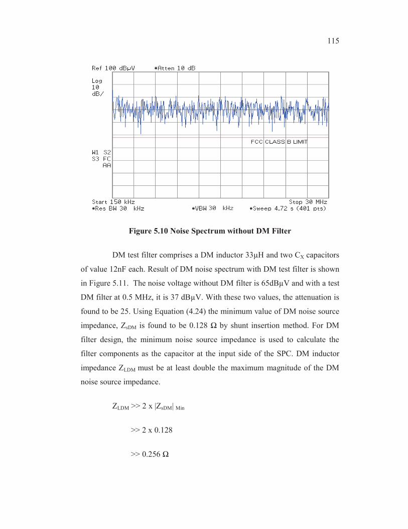
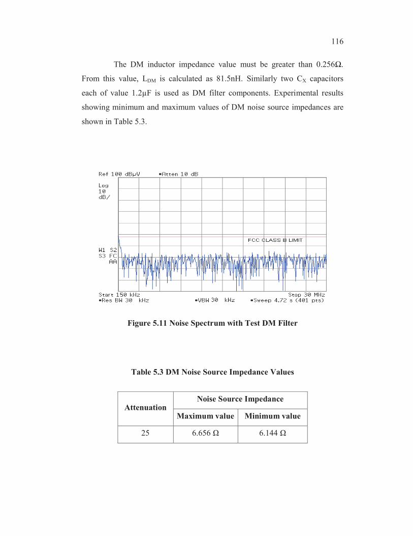
DM test filter comprises a DM inductor 33µH and two CX capacitors
of value 12nF each. Result of DM noise spectrum with DM test filter is shown
in Figure 5.11. The noise voltage without DM filter is 65dBµV and with a test
DM filter at 0.5 MHz, it is 37 dBµV. With these two values, the attenuation is
found to be 25. Using Equation (4.24) the minimum value of DM noise source
impedance, ZsDM is found to be 0.128 by shunt insertion method. For DM
filter design, the minimum noise source impedance is used to calculate the
filter components as the capacitor at the input side of the SPC. DM inductor
impedance ZLDM must be at least double the maximum magnitude of the DM
noise source impedance.
ZLDM >> 2 x |ZsDM| Min
>> 2 x 0.128
>> 0.256
116
The DM inductor impedance value must be greater than 0.256 .
From this value, LDM is calculated as 81.5nH. Similarly two CX capacitors
each of value 1.2µF is used as DM filter components. Experimental results
showing minimum and maximum values of DM noise source impedances are
shown in Table 5.3.
Figure 5.11 Noise Spectrum with Test DM Filter
Table 5.3 DM Noise Source Impedance Values
AttenuationNoise Source Impedance
Maximum value Minimum value
25 6.656 6.144
117
5.3.3 Selection of DM Filter Components
The minimum DM noise source impedance is used for the filter
design because an X capacitor is used at the input of the SPC. The attenuation
of this DM filter topology is expressed using Equation (5.8), where ZC1 and
ZCs are given by Equations (5.9) and (5.10), respectively. In Equations (5.9)
and (5.10), ZCX is the X capacitor impedance and in Equation (5.8), ZLDM is the
DM inductance impedance. In Equations (5.8) and (5.9), RloadDM is the
equivalent load resistance of LISN which is 100 .
loadDM sDM C1 LDM CsTDM
loadCM sDM Cs C1
R Z (Z + Z + Z )A =
(R + Z ) Z Z (5.8)
loadCM CXC1
loadCM CX
R ZZ =
R + Z (5.9)
CX sDMCs
CX sDM
Z ZZ =
Z + Z (5.10)
With the results obtained, the lowest spot frequency needed is
F0 = 500 KHz. The attenuation needed at this frequency is 7.9. The DM
inductance is used as leakage inductance of the CM inductor; hence single
inductor is needed to meet the required attenuation for the CM and the DM
noise. Equation (5.8) together with LDM = 33µH, ZsDMmin = 0.128 , and CX =
22nF, the estimated attenuation ATDM is 9.8 at F0 = 500 KHz, bigger than the
required attenuation which is 7.5. The test result of the noise spectrum after the
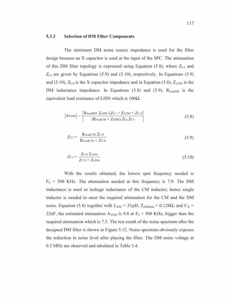
designed DM filter is shown in Figure 5.12. Noise spectrum obviously exposes
the reduction in noise level after placing the filter. The DM noise voltage at
0.5 MHz are observed and tabulated in Table 5.4.
118
Figure 5.12 Noise Spectrum with DM Filter
Table 5.4 DM Noise Voltages
Topology Noise Voltage
Without DM filter 65 dBµV
With test DM filter 37 dBµV
With DM filter 26 dBµV
5.4 DESIGN OF EMI FILTER
CM and DM filters are designed separately in the previous
procedures. Now, both the filters are assembled together to get a complete
EMI filter. The procedure to design EMI filter is summarized as follows.
STEP 1: Separate the CM and DM noise spectrum of the SPC.
STEP 2: Determine the noise voltage, Vnoise, without and with a single
filter (example, a capacitor).
119
STEP 3: Calculate the maximum CM and DM noise source impedances
for the frequency range of interest (0.15–30 MHz for the FCC
class B).
STEP 4: Design the EMI filter with maximum or minimum value of the
noise source impedance which contains the least attenuation.
STEP 5: The completed EMI filter is analyzed.
This procedure agrees that the CM and DM noises that arise from
different sources are effectively suppressed. The final EMI filter is illustrated
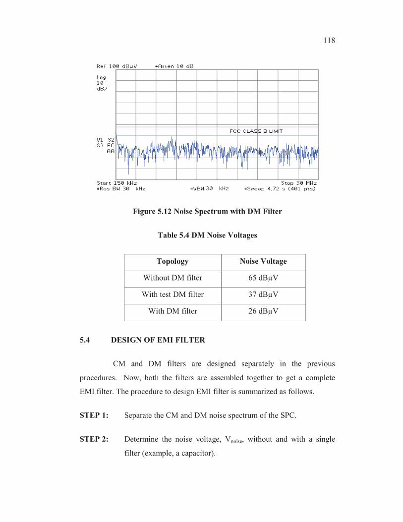
in Figure 5.13.
18µH
110V AC
InputCx1
22µF
LDM
33µH
Leakage
Inductance
LCM1 LCM2
33 H 33 H
CY
CY
47nF
47nF
Cx2
22µF
Output
º º
º º
Figure 5.13 Complete EMI Filter
A 220-µF electrolytic capacitor is connected at the output of the
filter. This makes that the EMI filter strengthens the feedback loop of the SPC.
It does not concern the filter design because the resonant frequency of this
electrolytic capacitor is comparatively small. This filter is arranged by ceramic
capacitors and CM inductors. The relevant value of capacitors CY is 47nF and
CX is 22µF.
The inductor used in EMI filter has a value of 33µH and current
rating of 3A. The number of windings is 79. Similarly capacitance has a
voltage rating of 400V and the ESR requirements are 1.2 . Noise spectrum
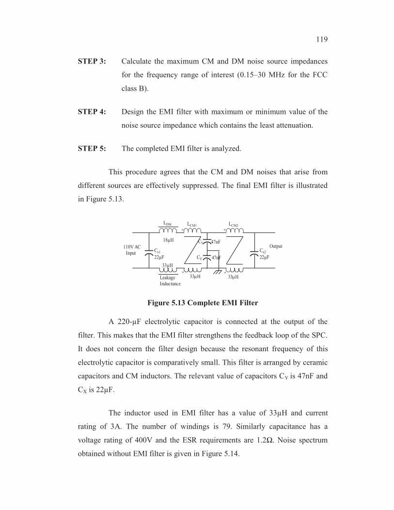
obtained without EMI filter is given in Figure 5.14.
120
Figure 5.14 Noise Spectrum without EMI Filter
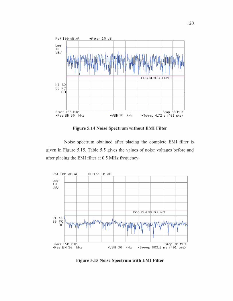
Noise spectrum obtained after placing the complete EMI filter is
given in Figure 5.15. Table 5.5 gives the values of noise voltages before and
after placing the EMI filter at 0.5 MHz frequency.
Figure 5.15 Noise Spectrum with EMI Filter

121
Table 5.5 EMI Noise Voltages
Topology Noise Voltage
Without EMI filter 72 dBµV
With EMI filter 28 dBµV
FCC class B standards recommend the Conducted noise emission
limit as 48 dBµV. Conducted noise emission without EMI filter is 72 dBµV
and with EMI filter is 28 dBµV which is very much below the limit of the
FCC class A and class B standards. So the standard regulation is well satisfied.
Thus by matching the filter parameters with noise source impedance an
efficient EMI filter is designed.
5.5 X2Y FILTER
The complete EMI filter using X2Y is illustrated in Figure 5.16.
X2Y replaces five to seven standard passive elements used for the purpose of
noise cancellation. Standard two termination capacitors are made of two
opposing electrodes that are screened onto layers of dielectric material in an
alternating fashion during the fabrication process. X2Y capacitor circuit
configurations and physical structure are shown in Figure 5.17. The X2Y filter
used is the Johnson Dielectrics catalogue no. 501H47W102KF4T-AC.
POWER
RETURN
GND
Figure 5.16 X2Y Circuit
122
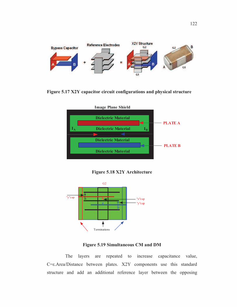
Figure 5.17 X2Y capacitor circuit configurations and physical structure
dielc
Dielectric Material
Dielectric Material
Dielectric Material
Dielectric Material
Image Plane Shield
IA IB
PLATE B
PLATE A
Figure 5.18 X2Y Architecture
Terminations
"x"cap
"y"cap
"y"cap
G2
Figure 5.19 Simultaneous CM and DM
The layers are repeated to increase capacitance value,
C= .Area/Distance between plates. X2Y components use this standard
structure and add an additional reference layer between the opposing
123
electrodes. A single X2Y component can provide the needed filtering to meet
less stringent FCC EMC compliance at a lower cost than conventional EMI
filter measures.
The X2Y architecture as shown in Figure 5.18 uses image planes
(shields), which create rectangular current loops that share a common image
plane. The X2Y plates A and B charge the image plane with opposing skin
currents. When the currents are common on the image plane or 180º out of
phase, they are oppositely charged and get cancelled.
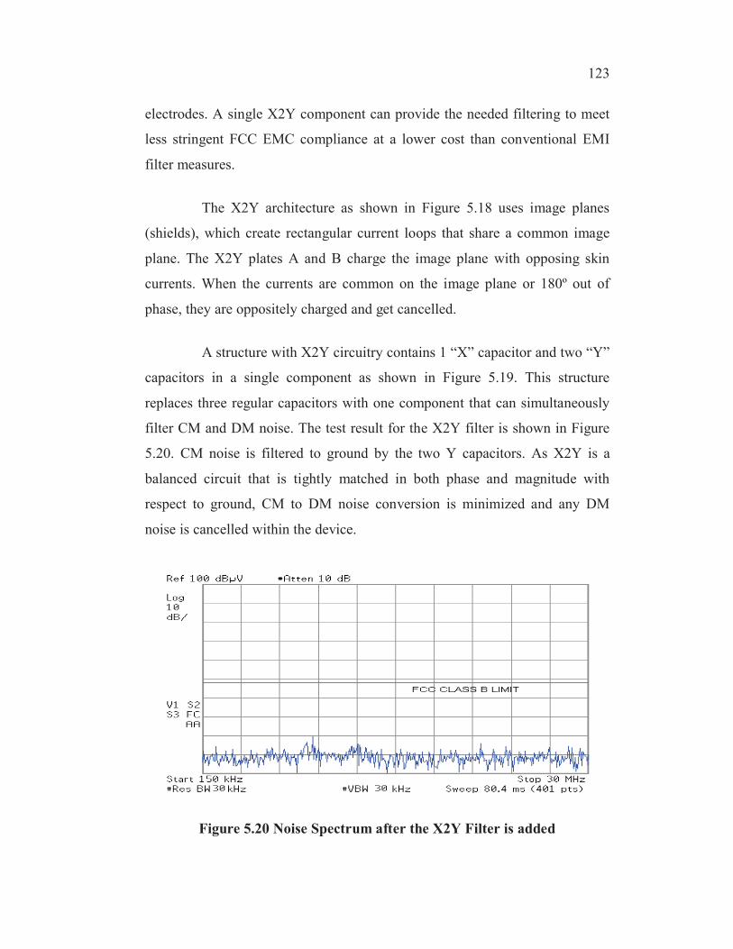
A structure with X2Y circuitry contains 1 “X” capacitor and two “Y”
capacitors in a single component as shown in Figure 5.19. This structure
replaces three regular capacitors with one component that can simultaneously
filter CM and DM noise. The test result for the X2Y filter is shown in Figure
5.20. CM noise is filtered to ground by the two Y capacitors. As X2Y is a
balanced circuit that is tightly matched in both phase and magnitude with
respect to ground, CM to DM noise conversion is minimized and any DM
noise is cancelled within the device.
Figure 5.20 Noise Spectrum after the X2Y Filter is added
124
5.5.1 High Frequency Decoupling Capacitor Requirements
The power distribution system on a PC board must provide a low
impedance source over a very wide frequency range. Various size decoupling
capacitors are typically mounted on the PC board for frequencies up to a few
hundred MHz. At frequencies above a few hundred MHz, the parallel plate
capacitance of the PC board power planes take over and provide the low
impedance source.
Small capacitors are used to cover the high frequency range just
below the point that requires internal PCB plane capacitance. The most
important characteristic of a high frequency decoupling capacitor is the ESL
(Equivalent Series Inductance). The ESL of interest is the effective
inductance of the capacitor including the surface footprint and via necessary
to connect to the internal power planes of the PCB. With lower ESL, fewer
decoupling capacitors (in parallel) are required to provide the low impedance
at high frequencies.
Depending on currents and voltages there are many different forms
of decoupling. The major application driving the need for improved
decoupling in the past decade has been the decoupling of the power supply
for high-speed microprocessors in electronic data processing applications.
Power Systems for modern CMOS technology are becoming harder to design.
The design methodology is to identify a target impedance to be
met across a broad frequency range and specify components to meet that
impedance. Given the voltage and power consumed, the current is calculated
from Ohm’s Law. Assuming that only a small percentage of the power supply
voltage (e.g. 5%) is allowed as ripple voltage (noise), target impedance for
the PDS is calculated. The target impedance is falling at an alarming rate, 5X
per computer generation and has now reached mOhm and sub mOhm levels.
125
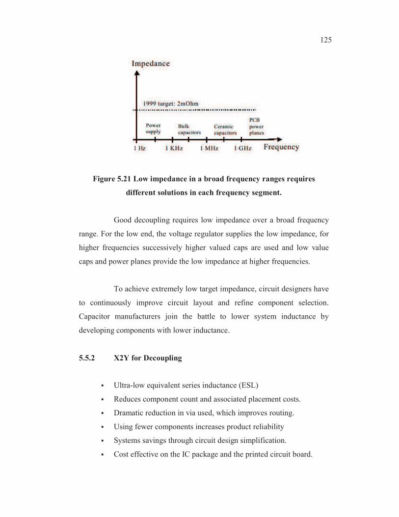
Figure 5.21 Low impedance in a broad frequency ranges requires
different solutions in each frequency segment.
Good decoupling requires low impedance over a broad frequency
range. For the low end, the voltage regulator supplies the low impedance, for
higher frequencies successively higher valued caps are used and low value
caps and power planes provide the low impedance at higher frequencies.
To achieve extremely low target impedance, circuit designers have
to continuously improve circuit layout and refine component selection.
Capacitor manufacturers join the battle to lower system inductance by
developing components with lower inductance.
5.5.2 X2Y for Decoupling
Ultra-low equivalent series inductance (ESL)
Reduces component count and associated placement costs.
Dramatic reduction in via used, which improves routing.
Using fewer components increases product reliability
Systems savings through circuit design simplification.
Cost effective on the IC package and the printed circuit board.
126
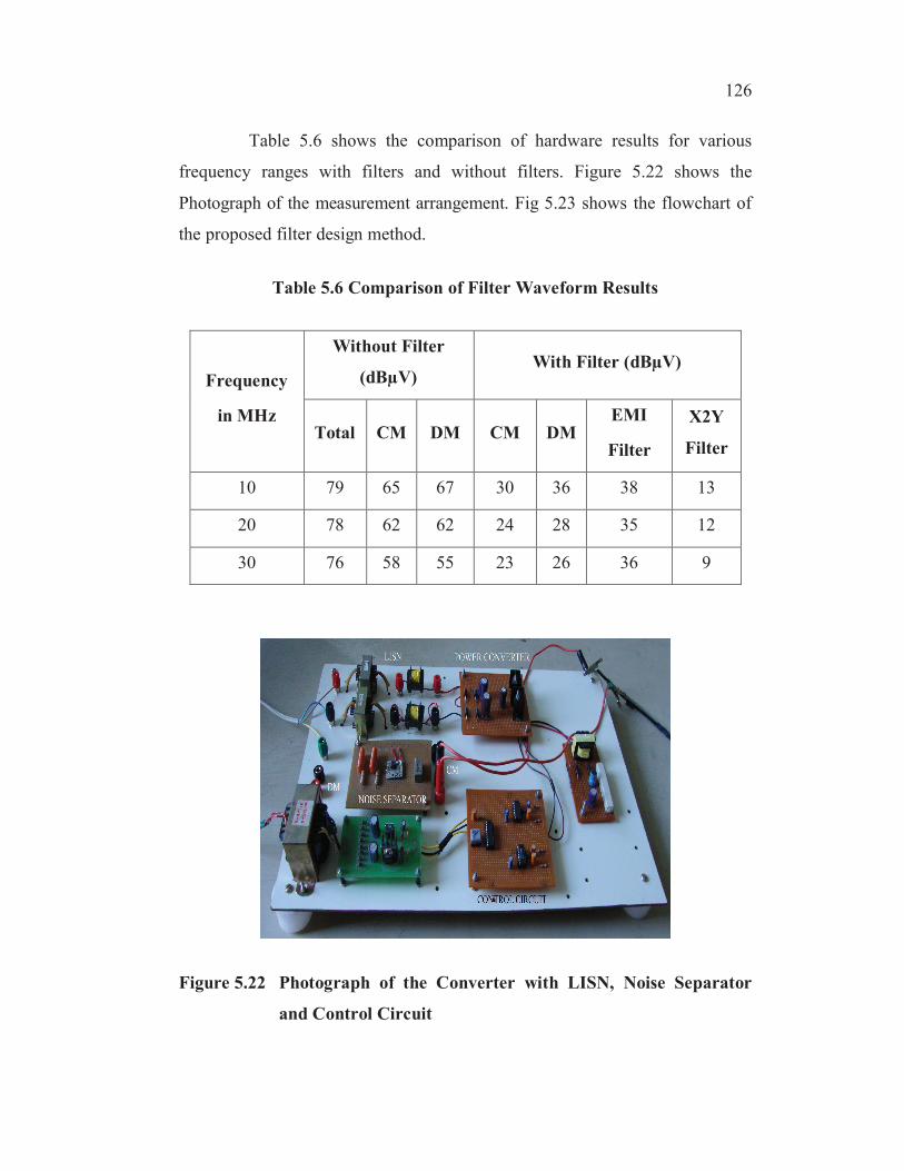
Table 5.6 shows the comparison of hardware results for various
frequency ranges with filters and without filters. Figure 5.22 shows the
Photograph of the measurement arrangement. Fig 5.23 shows the flowchart of
the proposed filter design method.
Table 5.6 Comparison of Filter Waveform Results
Frequency
in MHz
Without Filter
(dBµV)With Filter (dBµV)
Total CM DM CM DMEMI
Filter
X2Y
Filter
10 79 65 67 30 36 38 13
20 78 62 62 24 28 35 12
30 76 58 55 23 26 36 9
Figure 5.22 Photograph of the Converter with LISN, Noise Separator
and Control Circuit

127
Separate the DM and
CM noise spectra
Determine the requiredattenuation for DM and
CM noise
Calculate the Max and
Min DM and CM noise
impedances
Select CM and DM
filter topologies
Calculate the CM and
DM filter corner
frequencies
Use the worst case
noise impedance to
calculate the requiredattenuation for the CM
and DM topologies
Select components
and test CM filter
Assemble DM
and CM filters
Test the
complete filter
Results
acceptable?
Select components
and test DM filter
Results
acceptable?
Results
acceptable?
Select
lower
corner
frequency
or another
topology
Select
another
topology
End
Step 1
Step 2
Step 3
Step 4
Step 5
Step 6
Step 7
Step 8
Step 9
Step 10
Low freq
spec not
met?
CM DM
YesYes
Yes
Yes
No No
No
No
Figure 5.23 Flowchart of the Proposed Filter Design Method

128
Design methods ensure complete decoupling of the characteristics of
the CM and DM filters that are combined to produce the X2Y design. The
transfer functions of the combined filter ensure that the frequency responses
expected of the individual sub filters are retained.
The parametric study on the combined X2Y filter discovers capacitor
variations have biggest effects to degrade the performance of the filter. The
X2Y filter affects the steady-state waveforms, Input-output characteristics
and the dynamic response of the Switching Power Converters.
5.6 CONCLUSION
The procedure of designing an enhanced and simple method of EMI
filter depends on the noise spectrum and with the measured data to determine
the maximum and minimum magnitude of the noise source impedance used in
the EMI filter design. The CM and DM filters are designed individually. For
the CM part of the EMI filter, two types of filters are considered. In the first
type, the CM inductor appears at the input side of SPC. In the second type, the
X capacitor appears at the input side of SPC. A type filter is used to restrain
the DM noise, since this type presents improved performance than other types
for example, LC type. At last, the CM and DM filters are collected together to
get the total EMI filter. The X2Y filter provides considerable perfection in
reducing the Conducted emissions while compared to four mica filter
arrangements. From these results X2Y filter is found to be better than other
filters taken for analysis in this thesis.