Embed Size (px)
Citation preview
8/7/2019 Reduction of Conducted EMI in SMPS Using EMI Filter
http://slidepdf.com/reader/full/reduction-of-conducted-emi-in-smps-using-emi-filter 1/6
Abstract almost every electronic device requires some level
of power conversion in which the required operational voltagesare generated from the input power. Using switched mode
power supply (SMPS) for this purpose generates higher level of conducted EMI in the high frequency range and it negatively
affects the performance of other near by electronics. Soprediction of conducted EMI is necessary. Time domain
simulation plus Fast Fourier Transform (FFT) is a good methodto predict the conducted EMI. In this paper the Boost PFCcircuit is modeled considering parasitic parameters for all the
components. This circuit is simulated using PSPICE and theconducted EMI is predicted. The EMI filter is one of the
techniques to reduce the conducted EMI. The combined CMand DM mode filter configuration is discussed. For different
filter component values the circuit is simulated using PSPICE.A better configuration is suggested from the simulated models.
Index TermsCommon mode (CM), differential mode (DM),
electromagnetic interference (EMI), PFC converter
I. INTRODUCTION
An electromagnetic disturbance is any electromagneticphenomenon which may degrade the performance of a deviceor equipment or a system. The electromagnetic disturbancecan be in nature of the electromagnetic noise, or an unwantedsignal, or a change in the propagation medium itself.Electromagnetic interference is the degradation in theperformance of a device or equipment or a system caused byan electromagnetic disturbance. So improve the performanceof a device or equipment or a system the EMI has to bereduced.In [1] the conducted EMI of the CCM PFC circuit ispredicted using a simulation circuit also DM and CM loopmodels of the PFC EMI are proposed for describing the noisegeneration and propagation mechanisms. It also describes theeffects of PFC inductor and the parasitic capacitances at theMOSFET drain node.The EMI spectrum of a discontinuous conduction mode PFCconverter is predicted using a simulation circuit in saber in[2]. It also gives the design guide lines on circuit layout andpackaging for EMI noise minimization. In [3] the frequencydomain analysis of the boost PFC is explained. In that paper
the noise sources and all other circuit componexpressed as functions in the frequency domain and thepredicted EMI spectrum is calculated by solving the matrixesformed by these functions.
The common mode and differential mode switching noisetogether with the input filter design and lot of designconsiderations such as printed circuit board layout, the effectof gate snubber, the shield inserted between the device and
the heat sink and also the heat sink grounding connectionsare described in [4]. It also reports the conducted EMImeasurements for different filter capacitor values andplacements, for different power switch drive circuits whichturned out to be decisive factors in the reduction of thegenerated EMI.
In [5] PFC noise source characteristics and its effect on EMInoise, impedance mismatch and filter parasitic parametersare discussed. PFC DM and CM noise source models andtheir characteristics are analyzed. A filter is built and theanalysis is verified.
The basics of conducted EMI measurement, supprestechniques and discussed in [6].it also explains how to designfilter theoretically and making modifications using practicalapproach to get a fast and accurate filter solution. In [7] a very practical EMI filter design according to militarystandard MIL-STD 461 is discussed. In [8] design procedurefor ac line EMI filters are discussed. This procedure is basedon the analysis of conducted EMI problems and the use of EMI diagnostic tool, noise separator.
EMC design aspects for high power ac/dc rectifier and somedesign guide lines are discussed in [9].other papers in thissubject includes[10],[11],[12] and so on.
An overview of boost PFC circuit, parasitic model of boostPFC components are described in section II. Prediction of conducted EMI using simulation circuit is explasection III. Section IV explains CM and Darrangement and different filter configurations. Section Vconcludes the work.
II. PARASITIC MODEL OF BOOST CONVERTER
Reduction of Conducted EMI in SMPS usingEMI Filter
Document By
SANTOSH BHARADWAJ REDDYEmail: [email protected] Papers and Presentations available on above site
1
8/7/2019 Reduction of Conducted EMI in SMPS Using EMI Filter
http://slidepdf.com/reader/full/reduction-of-conducted-emi-in-smps-using-emi-filter 2/6
COMPONENTS
Fig 1 shows the simulation circuit in PSPICE for BoostPFC. Diodes used here are MUR140; the input is ac 220V,50 Hz. The MOSFET used here is IRPF450.The gate drivingcircuit is 100 KHz, square pulse generator. In the On-state,i.e., MOSFET is turned ON, resulting in an increase in theinductor current; thereby energy is stored in the inductor.Inthe Off-state, i.e., MOSFET is turned OFF, and the only path
offered to the inductor current is fly back diode D5, thecapacitor C1 and the load R1. This result in transferring theenergy accumulated during the On-state into the capacitor.The Boost PFC can be operated in two modes. One iscontinuous conduction mode and another one isdiscontinuous conduction mode.
D 6
M U R 1 4 0
D 7
M U R 1 4 0
D 8
M U R 1 4 0
D 9
M U R 1 4 0
D 1 1
M U R 1 4 0
1 2
L 1
3 2 0 u
C
1V 1
F R E Q = 5 0
V A M P L = 2 2 0
V O F F = 0
V 2
T D = 0
T F = 0 . 0 1 u
P W = 5 u
P E R = 1 0 u
V 1 = 1 0
T R = 0 . 0 1 u
V 2 = 0
0
M 3
I R F P 4 5 0
V -
V +
V -
V +
Fig 1. Boost PFC circuit for simulation
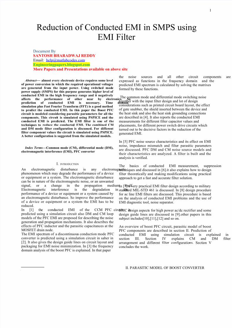
Fig 2. Output of the Boost PFC
The simulated output wave form is shown in fig 2.The output is about 475V dc. Thus the converter boosts theinput 220V ac to 475V dc with 2.15 percent of Boost factor.
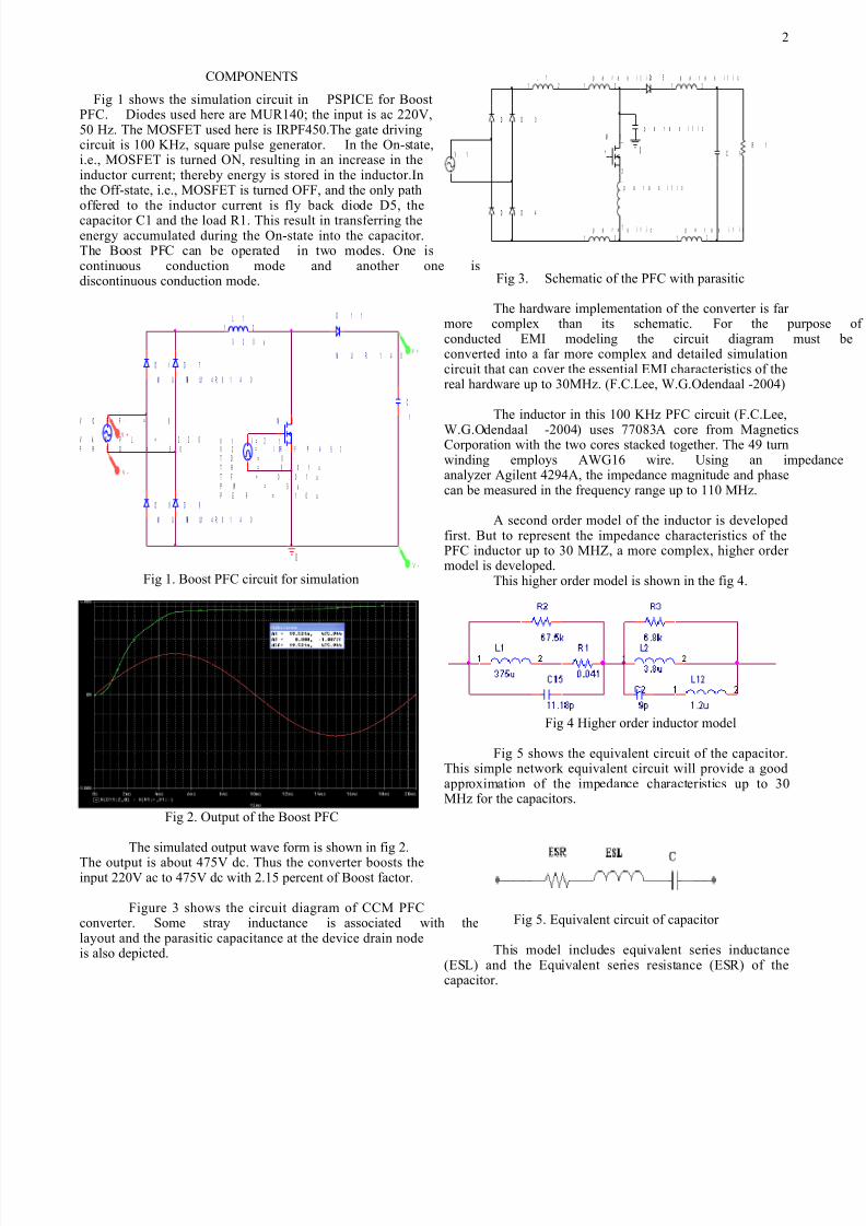
Figure 3 shows the circuit diagram of CCM PFCconverter. Some stray inductance is associated with thelayout and the parasitic capacitance at the device drain nodeis also depicted.
p a r a s i t i c1 2
D 2
M 1
1
2
3
p a r a s i t i c1 2
0
D 3
p a r a s i t i c1 2
D 5
p a r a s i t i c
1
2
p a r a s i t i c1 2
D 4
p a r a s i t i c
C 1V 1
R 1
L 11 2
D 1
Fig 3. Schematic of the PFC with parasitic
The hardware implementation of the converter is far more complex than its schematic. For the puconducted EMI modeling the circuit diagram mconverted into a far more complex and detailed simulationcircuit that can cover the essential EMI characteristics of thereal hardware up to 30MHz. (F.C.Lee, W.G.Odendaal -2004)
The inductor in this 100 KHz PFC circuit (F.C.Lee,W.G.Odendaal -2004) uses 77083A core from MagneticsCorporation with the two cores stacked together. The 49 turnwinding employs AWG16 wire. Using an impanalyzer Agilent 4294A, the impedance magnitude and phasecan be measured in the frequency range up to 110 MHz.
A second order model of the inductor is developedfirst. But to represent the impedance characteristics of thePFC inductor up to 30 MHZ, a more complex, higher order model is developed.
This higher order model is shown in the fig 4.
Fig 4 Higher order inductor model
Fig 5 shows the equivalent circuit of the capacitor.This simple network equivalent circuit will provide a goodapproximation of the impedance characteristics up to 30MHz for the capacitors.
Fig 5. Equivalent circuit of capacitor
This model includes equivalent series inductance(ESL) and the Equivalent series resistance (ESR) of thecapacitor.
2
8/7/2019 Reduction of Conducted EMI in SMPS Using EMI Filter
http://slidepdf.com/reader/full/reduction-of-conducted-emi-in-smps-using-emi-filter 3/6
The capacitance, ESR, ESL are 125.9nF, 26.2 milliohms, 7.0nH respectively as shown in fig 6. In the realhardware another ceramic capacitor is paralled with theoutput capacitor (F.C.Lee, W.G.Odendaal -2004).
Fig 6. Capacitor model
LISN presents defined standard impedance to the EUT power
input terminals at high frequencyAny incoming unwanted conducted EMI on the mains power supply is filtered out by the LISN and a clean input power supply is provided to the EUT
Figure 7 shows a LISN circuit used in thissimulation model.
Fig 7. LISN model
III PREDICTION OF CONDUCTED EMI IN BOOST PFCCIRCUIT
Figure 8 shows the detailed simulation circuit, consideringall the parasitic parameters.Input is 220V ac supply with a frequency of 50 Hz. Thediodes used in the simulation are MUR140.The inductor and
the capacitor is considered with parasitic models.The MOSFET circuit used in the simulation is IRPF450.thegate drain parasitic parameters also modeled. The gate drivecircuit used here is a square pulse generator with a frequencyof 100 KHz
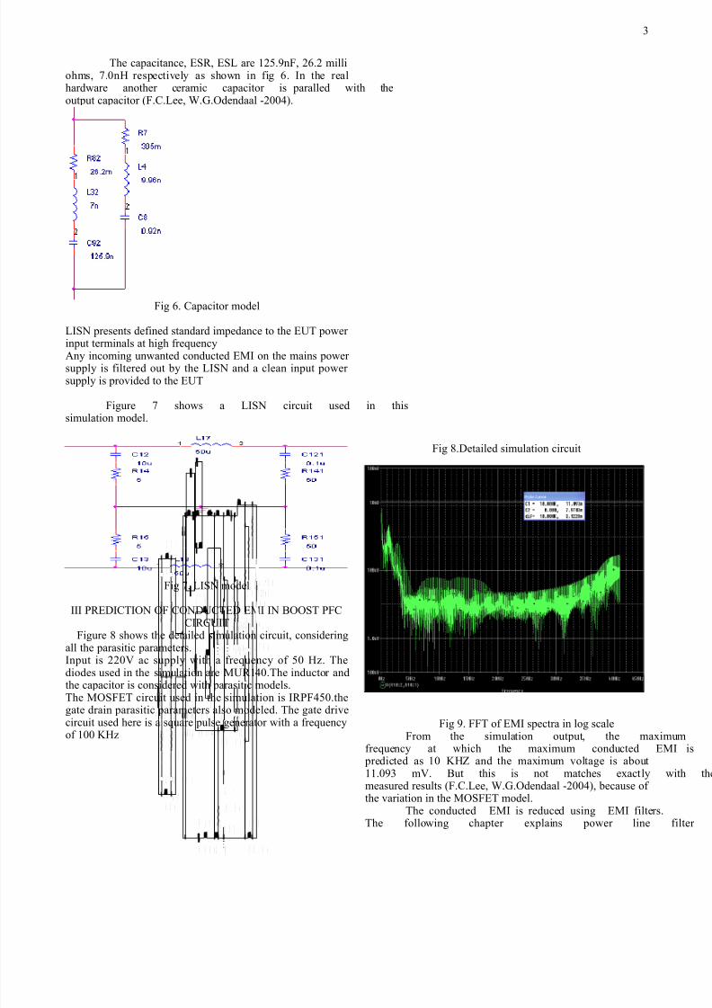
Fig 8.Detailed simulation circuit
Fig 9. FFT of EMI spectra in log scaleFrom the simulation output, the max
frequency at which the maximum conducted Epredicted as 10 KHZ and the maximum voltage is about11.093 mV. But this is not matches exactly measured results (F.C.Lee, W.G.Odendaal -2004), because of the variation in the MOSFET model.
The conducted EMI is reduced using EMI filtersThe following chapter explains power line
3
C 2
9 p
C 8
0 .9 2 n
C 9 21 2 5 . 9 n
C 1 4
2 7 9 u
C 1 5
1 1 .1 8 p
D 1
M U R 1 4 0
D 2
M U R 1 4 0
D 3
M U R 1 4 0
D 4
M U R 1 4 0
D 5
M U R 1 4 01 2
L 1
3 7 5 u1 2
L 2
3 .8 u
1
2
L 3 2
7 n
1
2
L 4
9 .9 6 n
1 2
L 6
1 9 n1 2
L 7
1 4 . 1 n1 2
L 8
4 9 .5 n
1
2
L 1 0
1 0 . 6 n
1 2L 1 2
1 . 2 u
R 1
0 .0 4 1
R 2
6 7 .5 k
R 3
6 . 8 k
R 6
1 5 0 mR 7
3 0 5 m
R 8 2
2 6 . 2 m
R 1 0
1 5 0
1
2
L 3 1
9 .9 6 n
C 9 1
0 .9 2 n
R 8 1
3 0 5 m
C 9
1 2 5 . 9 n
1
2
L 3
7 n
R 8
2 6 .2 m
1 2L 5
6 5 n
1
2
L 9
8 . 5 n
C 1 0
2 2 .7 p
C 1 1
2 2 . 7 p
1 2L 1 1
4 7 . 6 n
1 2L 1 3
3 9 . 5 n
1 2L 1 4
2 . 7 n
R 9
1 0 0 0 k
00
R 1 1
3
R 1 2
9
1 2L 1 5
2 6 n
1 2L 1 6
9 .9 n
R 1 3
0 . 1
V 1
F R E Q =5 0A M P L = 2 2 0O F F = 0
V 2
T D = 0
T F =0 .0 1 uP W = 5 uP E R =1 0 u
V 1 = 1 0
T R = 0 . 0 1 u
V 2 = 0
R 1 4
5
R 1 5
5
C 1 2
1 0 u
C 1 3
1 0 u
1 2L 1 7
5 0 u
1 2L 1 8
5 0 u
C 1 2 1
0 .1 u
R 1 4 1
5 0
R 1 5 1
5 0
C 1 3 1
0 .1 u
0
M 3
I R F P 4 5 0
M 4
I R F P 4 5 0
1 2L 1 9
1 0 . 9 n0
V -
V +
8/7/2019 Reduction of Conducted EMI in SMPS Using EMI Filter
http://slidepdf.com/reader/full/reduction-of-conducted-emi-in-smps-using-emi-filter 4/6
configuration and this filter configuration with various valuesof filter components are simulated.
IV REDUCTION OF CONDUCTED EMI USING EMIFILTERS
EMI filter is connected in between the LISN and the diodebridge rectifier of the Boost PFC. EMI filter configuration issimulated for various values of filter components. Five such
filter configurations are simulated in this section. For theclear depiction of the filters only the simulation circuit of thefilters is shown in all cases. The detailed simulation circuit of the Boost PFC and LISN is not shown in all cases.
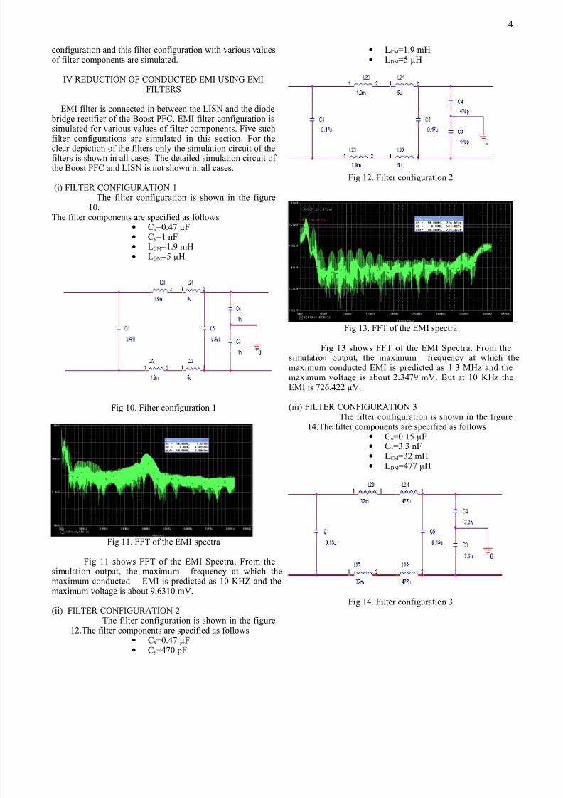
(i) FILTER CONFIGURATION 1The filter configuration is shown in the figure
10.The filter components are specified as follows
• Cx=0.47 µF• Cy=1 nF• LCM=1.9 mH• LDM=5 µH
Fig 10. Filter configuration 1
Fig 11. FFT of the EMI spectra
Fig 11 shows FFT of the EMI Spectra. From thesimulation output, the maximum frequency at which themaximum conducted EMI is predicted as 10 KHZ and themaximum voltage is about 9.6310 mV.
(ii) FILTER CONFIGURATION 2The filter configuration is shown in the figure
12.The filter components are specified as follows• Cx=0.47 µF• Cy=470 pF
• LCM=1.9 mH• LDM=5 µH
Fig 12. Filter configuration 2
Fig 13. FFT of the EMI spectra
Fig 13 shows FFT of the EMI Spectra. From thesimulation output, the maximum frequency at which themaximum conducted EMI is predicted as 1.3 MHz and themaximum voltage is about 2.3479 mV. But at 10 KHz theEMI is 726.422 µV.
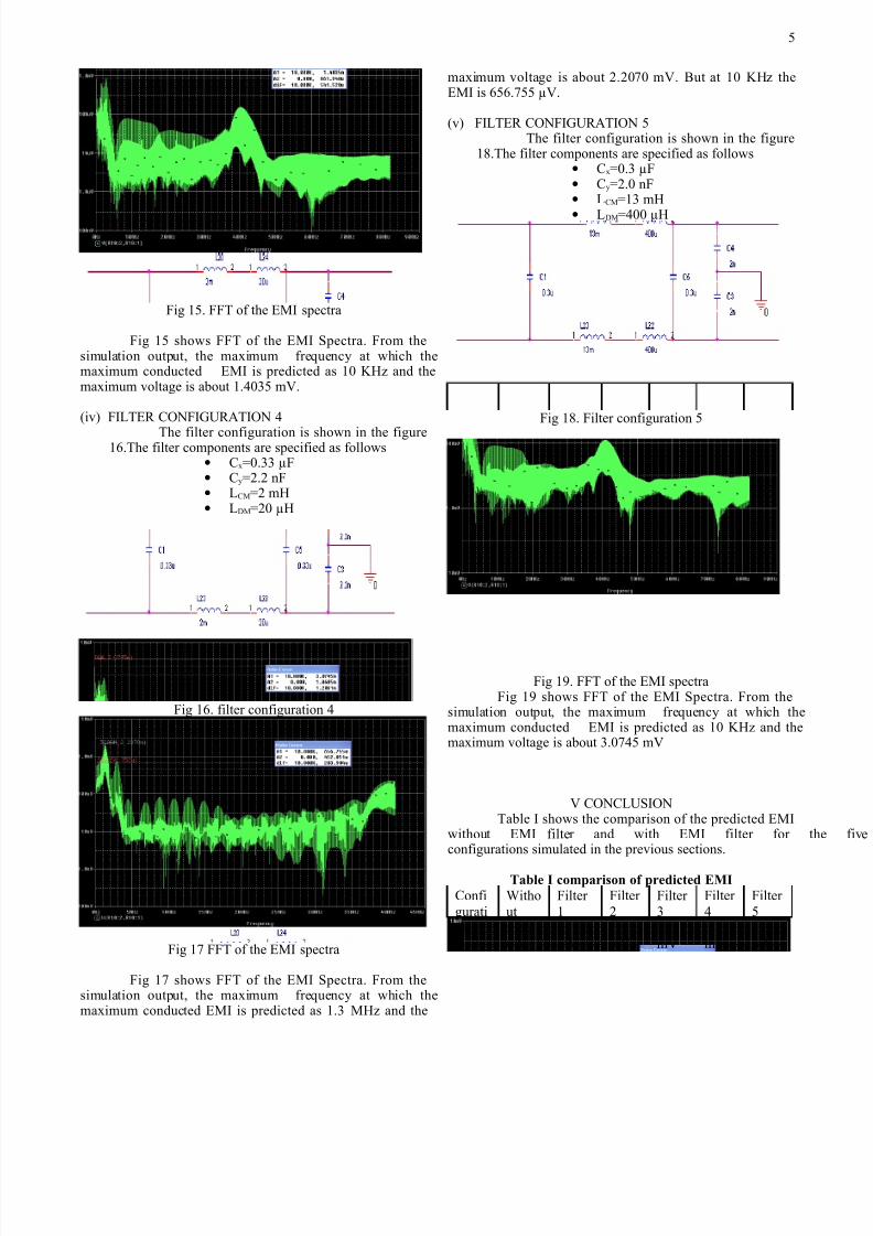
(iii) FILTER CONFIGURATION 3The filter configuration is shown in the figure
14.The filter components are specified as follows• Cx=0.15 µF• Cy=3.3 nF• LCM=32 mH• LDM=477 µH
Fig 14. Filter configuration 3
4
8/7/2019 Reduction of Conducted EMI in SMPS Using EMI Filter
http://slidepdf.com/reader/full/reduction-of-conducted-emi-in-smps-using-emi-filter 5/6
Fig 15. FFT of the EMI spectra
Fig 15 shows FFT of the EMI Spectra. From thesimulation output, the maximum frequency at which themaximum conducted EMI is predicted as 10 KHz and themaximum voltage is about 1.4035 mV.
(iv) FILTER CONFIGURATION 4The filter configuration is shown in the figure16.The filter components are specified as follows
• Cx=0.33 µF• Cy=2.2 nF• LCM=2 mH• LDM=20 µH
Fig 16. filter configuration 4
Fig 17 FFT of the EMI spectra
Fig 17 shows FFT of the EMI Spectra. From thesimulation output, the maximum frequency at which themaximum conducted EMI is predicted as 1.3 MHz and the
maximum voltage is about 2.2070 mV. But at 10 KHz theEMI is 656.755 µV.
(v) FILTER CONFIGURATION 5The filter configuration is shown in the figure
18.The filter components are specified as follows• Cx=0.3 µF• Cy=2.0 nF• LCM=13 mH• LDM=400 µH
Fig 18. Filter configuration 5
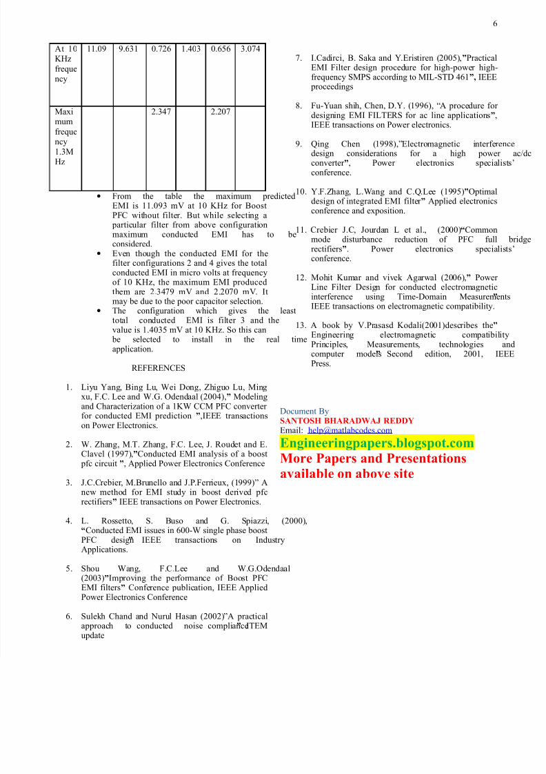
Fig 19. FFT of the EMI spectraFig 19 shows FFT of the EMI Spectra. From the
simulation output, the maximum frequency at which themaximum conducted EMI is predicted as 10 KHz and themaximum voltage is about 3.0745 mV
V CONCLUSIONTable I shows the comparison of the predicted EMI
without EMI filter and with EMI filter for configurations simulated in the previous sections.
Table I comparison of predicted EMI
Confi
gurati
on
Witho
ut
filter
mV
Filter
1
mV
Filter
2
mV
Filter
3
mV
Filter
4
mV
Filter
5
mV
5
8/7/2019 Reduction of Conducted EMI in SMPS Using EMI Filter
http://slidepdf.com/reader/full/reduction-of-conducted-emi-in-smps-using-emi-filter 6/6
At 10
KHz
freque
ncy
11.09 9.631 0.726 1.403 0.656 3.074
Maxi
mum
frequency
1.3M
Hz
2.347 2.207
• From the table the maximum predictedEMI is 11.093 mV at 10 KHz for BoostPFC without filter. But while selecting aparticular filter from above configurationmaximum conducted EMI has to beconsidered.
• Even though the conducted EMI for the
filter configurations 2 and 4 gives the totalconducted EMI in micro volts at frequencyof 10 KHz, the maximum EMI producedthem are 2.3479 mV and 2.2070 mV. Itmay be due to the poor capacitor selection.
• The configuration which gives the leasttotal conducted EMI is filter 3 and thevalue is 1.4035 mV at 10 KHz. So this canbe selected to install in the real timeapplication.
REFERENCES
1. Liyu Yang, Bing Lu, Wei Dong, Zhiguo Lu, Ming
xu, F.C. Lee and W.G. Odendaal (2004),” Modelingand Characterization of a 1KW CCM PFC converter for conducted EMI prediction ”,IEEE transactionson Power Electronics.
2. W. Zhang, M.T. Zhang, F.C. Lee, J. Roudet and E.Clavel (1997),”Conducted EMI analysis of a boostpfc circuit ”, Applied Power Electronics Conference
3. J.C.Crebier, M.Brunello and J.P.Ferrieux, (1999)” Anew method for EMI study in boost derived pfcrectifiers” IEEE transactions on Power Electronics.
4. L. Rossetto, S. Buso and G. Spiazzi, (2000),
“Conducted EMI issues in 600-W single phase boostPFC design” IEEE transactions on IndustryApplications.
5. Shou Wang, F.C.Lee and W.G.Odendaal(2003)”Improving the performance of Boost PFCEMI filters” Conference publication, IEEE AppliedPower Electronics Conference
6. Sulekh Chand and Nurul Hasan (2002)”A practicalapproach to conducted noise compliance” ITEMupdate
7. I.Cadirci, B. Saka and Y.Eristiren (2005),”PracticalEMI Filter design procedure for high-power high-frequency SMPS according to MIL-STD 461”, IEEEproceedings
8. Fu-Yuan shih, Chen, D.Y. (1996), “A procedure for designing EMI FILTERS for ac line applications”,IEEE transactions on Power electronics.
9. Qing Chen (1998),”Electromagnetic interferendesign considerations for a high power converter ”, Power electronics specialisconference.
10. Y.F.Zhang, L.Wang and C.Q.Lee (1995)”Optimaldesign of integrated EMI filter ” Applied electronicsconference and exposition.
11. Crebier J.C, Jourdan L et al., (2000)“Commonmode disturbance reduction of PFC full rectifiers”. Power electronics specialisconference.
12. Mohit Kumar and vivek Agarwal (2006),” Power Line Filter Design for conducted electromagneticinterference using Time-Domain Measuremen”IEEE transactions on electromagnetic compatibility.
13. A book by V.Prasasd Kodali(2001)describes the”Engineering electromagnetic compatibilitPrinciples, Measurements, technologies acomputer models” Second edition, 2001, IEEPress.
Document BySANTOSH BHARADWAJ REDDYEmail: [email protected]
Engineeringpapers.blogspot.comMore Papers and Presentationsavailable on above site
6