Embed Size (px)
Citation preview

Chapter 3 77
Chapter 3
PEBB SYSTEM INTEGRATION ISSUES
3.1 Introduction
Stability and interaction problems are a major concern in a DC DPS because of the
distributed filter interaction on the bus [3],[4]. Modeling and control of PEBB based power
converters has been discussed in the previous chapter. After designing the subsystems they are
integrated to form the DC DPS. Even though the sub-systems may be well designed for stand-
alone operation, potential interaction problems are present when integrating the system.
This chapter presents the issues in integrating the PEBB based converters to form the
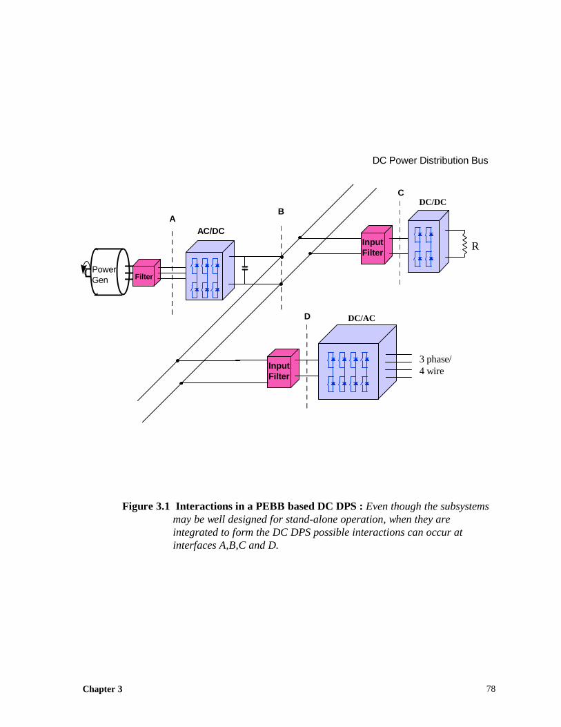
sample DC DPS shown in Figure 3.1. Each subsystem is designed to be stable and provide
Chapter 3 78
DC Power Distribution Bus
InputFilter
DC/AC
Power Gen Filter
AC/DC
3 phase/4 wire
R
DC/DC
InputFilter
AB
C
D
Figure 3.1 Interactions in a PEBB based DC DPS : Even though the subsystems may be well designed for stand-alone operation, when they are integrated to form the DC DPS possible interactions can occur at interfaces A,B,C and D.

Chapter 3 79
satisfactory transient response. The interaction between sub-systems and its effect on system
performance and stability is discussed. Section 3.2 presents an analysis of the effects of
impedance overlap. Ratio of impedances at the interface between subsystems is used to
determine system stability.
Referring to Fig. 3.1, interface A (EMI filter - Boost Rectifier), B (Output DC link -
load) , C (Input filter - DC/DC converter) and D (Input filter - Inverter) can be a cause of
instability and can cause large ringing and voltage transient on the bus. Interface A, B and D
are checked for stability by impedance comparison method as described in [3]. The interface C
has been discussed in great detail in the literature [14],[15] and is not discussed in this thesis.
The main limitation of the conventional DC DPS is its inability to deal with these
interaction problems. If large ringing and voltage overshoot occur on the DC bus due to sub-
system interaction, the fault protection scheme shuts down the entire system. The system has
to be dismantled and each subsystem is redesigned. This is a costly and time consuming
process. Whereas, a PEBB based DC DPS offers advantages like system re-configuration,
hierarchical control and control intelligence. A PEBB based system allows flexibility in system
operation and system configuration.
This chapter presents the ability of a PEBB based system in dealing with system
interaction issues. The potential stability problems in the sample DC DPS are presented. And,
the effect of changing PEBB system parameters like switching frequency, subsystem
bandwidth on the system performance and stability is investigated.
Chapter 3 80
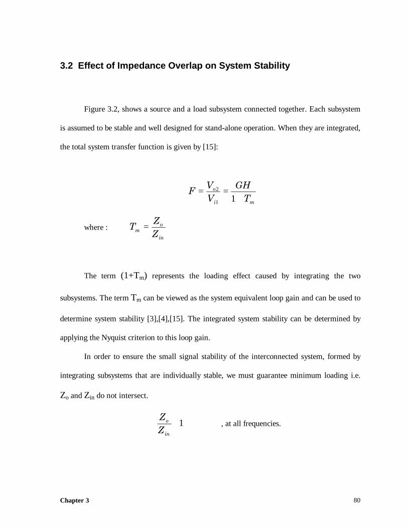
3.2 Effect of Impedance Overlap on System Stability
Figure 3.2, shows a source and a load subsystem connected together. Each subsystem
is assumed to be stable and well designed for stand-alone operation. When they are integrated,
the total system transfer function is given by [15]:
F VV
GHT
o
i m
= =+
2
1 1
where : T ZZm
o
in
=
The term (1+Tm) represents the loading effect caused by integrating the two
subsystems. The term Tm can be viewed as the system equivalent loop gain and can be used to
determine system stability [3],[4],[15]. The integrated system stability can be determined by
applying the Nyquist criterion to this loop gain.
In order to ensure the small signal stability of the interconnected system, formed by
integrating subsystems that are individually stable, we must guarantee minimum loading i.e.
Zo and Zin do not intersect.
ZZ
o
in
⟨⟨1 , at all frequencies.
Chapter 3 81
Subsystem 1 Subsystem 2
Zo Zin
Vo1 Vi2 Vo2Vi1 H VV
o2
i2
=G VV
o1
i1
=
F VV
GH
1 ZZ
o2
i1 o
in
= =+
Figure 3.2 Two Cascaded Subsystems : The integrated transfer function F depends on the ratio of output impedance of system1 (Zo) to input impedance of system2 (Zin).

Chapter 3 82
However, in most practical circuits it is not possible to achieve non-minimal interaction. If Zo
and Zin intersect then the impedance overlap must be analyzed for stability. The characteristic
equation of the overall system is :
1 0+ =Tm
A polar plot of the loop gain, Tm can be used to check system stability i.e. check if the plot
encircles (-1,0) point.
System interaction is a major concern in all power electronics systems as most load
converters behaves like a negative impedance (-R) below the loop gain crossover frequency
[15]. The phase characteristic of the active load (-R) is always -1800, and this can result in
system interaction.
Figure 3.3 shows an example where the input impedance of the load subsystem
interacts with the output impedance of the source subsystem. It is seen that |Zin| < |Zo| at
some frequencies. The loop gain Tm is used to check the system stability. The magnitude of
Tm is 0 dB at two frequencies and thus two phase margins can be defined and used to check
relative stability. These phase margins are defined at high-frequency and low-frequency
crossovers of impedance overlap.
In addition to stability, the loop gain Tm also gives information regarding the amount
of voltage overshoot on the bus and the settling time needed to recover from a change in
operating conditions [3]. If the loop gain Tm has a small relative stability margin, then there
will be significant voltage overshoot on the bus during transient conditions.

Chapter 3 83
|Tm|
Tm
Figure 3.3 Loop Gain Tm used to check System Stability : The loop gain Tm has two crossover frequencies. Low-frequency crossover at 140 Hz (Phase Margin = 300 ) and High-frequency crossover at 18 kHz (Phase Margin = 300 ).

Chapter 3 84
3.3 Input Filter - Subsystem Interaction
To meet the stringent requirements placed on EMI emission, most of the present days
power converters require an input EMI filter. Due to the complexity in modeling the converter
and input EMI filter together, they are usually designed separately. And, when integrated
together very often they may have interactions [3],[4].
In this section, the effect filter interaction has on the individual subsystems will be
examined and the ability of a PEBB based system in dealing with these interactions is studied.
As shown in Figure 3.1, the interfaces A,C and D can have potential interaction problems.
Interface C has been discussed in detail in the literature [14],[15] and is not discussed in this
thesis. This section investigates potential interaction problems at interfaces A and D, shown
in Figure 3.1.
3.3.1 Input EMI Filter and Front End Boost Rectifier Interface
The interface between input EMI filter and Boost Rectifier is tested for potential
interaction problems. Figure 3.4 shows the EMI filter and Boost Rectifier subsystem. The
system analysis technique described in the previous section concerns dc-dc converters and
cannot be applied directly in this case. A reduced model of three phase rectifiers, as shown in
Figure 3.5 has been discussed in the literature [16]. This new model converts a three phase

Chapter 3 85
Vo
LOAD
FILTER
3φ
CONTROLLER
Zo
Zin
(a) Zin and Zo at EMI filter and Boost Rectifier Interface
50 u
0.35 u 0.9 u 2
4.8 u5.7 u3.4 u
18 u17 u 20 u
Ω
(b) Input EMI filter
Figure 3.4 EMI filter and Boost Rectifier Interface : The impedance analysis technique for dc-dc converters , described in the previous section cannot be applied directly in this case.

Chapter 3 86
Vo
LOAD
C
Leq = 1.5 LPWM Cell
Veq = 2.06 Vph
(a) Reduced Order Model of the Boost Rectifier
ConverterReduced Order Model
EMI Filter
EMI Filter
EMI Filter
Zo Zin
(b) Impedance Comparison
Figure 3.5 Impedance Comparison using Reduced Order Model : The reduced order model converts the three phase rectifier into an equivalent dc-dc converter.
Chapter 3 87
rectifier into an equivalent second order dc-dc converter and this enables the use of impedance
comparison technique to determine system stability. Figure 3.5 shows the input impedance of
the reduced order model of Boost Rectifier (Zin) and the output impedance of EMI filter
(Zo).
Figure 3.6 shows the impedance overlap between the output impedance of the filter
and the input impedance of the rectifier. The input impedance Zin behaves like a negative
impedance at low frequency ( i.e. Phase is -180 degrees). It acts like a constant power load
due to closed loop regulation of the Boost Rectifier. After the loop crossover frequency, it
follows the open loop Zin plot. The Zo of the EMI filter is resistive at low frequency and then
it shows inductive characteristics. After that, there is resonance and then it behaves like a
capacitive impedance. For an optimally damped filter the resonant frequency of the filter
should be such that Zin and Zo do not interact. But, in most practical filter design it is not
possible and there is an impedance overlap.
As discussed in the previous section, the Nyquist criteria is checked for stability.
Figure 3.7 (a) shows the instability by applying the Nyquist criterion i.e. the plot encircles the
-1 point. Figure 3.7 (b) shows the time domain simulation results and large transients can be
seen in the input phase current waveforms.
The PEBB based system is able to avoid the instability by changing the controller
parameters. The instability is sensed by the controller and the switching frequency is doubled
from 20 kHz to 40 kHz. As the switching frequency is increased, it is possible to

Chapter 3 88
|Zin|
|Zout|
Mag
Phase
Zout
Zin
Figure 3.6 Impedance Overlap between Zo and Zin for Reduced Order Model: The input EMI filter has insufficient damping and this results in impedance overlap.

Chapter 3 89
(a) Nyquist plot for Zo/Zin
(b) Input currents drawn by the rectifier
Figure 3.7 Input Filter Rectifier Interaction : The switching frequency of the converter is 20 kHz. The switching model simulation shows system instability.
Chapter 3 90
increase the inner control loop bandwidth by increasing the proportional compensator gain. As
discussed in the previous section, the PEBB based converter has the ability to actively change
the gain of the controller. Changing the inner loop bandwidth changes the phase characteristic
of the input impedance and thus system instability is avoided.
Figure 3.8 (a) shows the Nyquist plot of the system with changed controller
parameters. The impedance overlap still exists but phase characteristics have been changed
such that the plot does not encircle the (-1,0) point. The system is shown to be stable and this
is confirmed by the time domain simulation. Figure 3.8 (b) shows the input current drawn by
the rectifier in the steady state. Compared to the original case, the peak to peak ripple has
been reduced to half as the switching frequency has been doubled.
This scheme suffers from the disadvantage that increasing the switching frequency
increases the switching losses in the power devices. Thus, the power devices and the heat sink
design must take this into account. Boost Rectifier supplies power to the DC link and in
certain applications it may be necessary to maintain continuous power flow even if it means
extra losses in the rectifier. In a conventional system, filter subsystem interactions can be
solved only through shutting down the system and redesigning the input filter. Where as
PEBB based rectifier provides an option for an online system reconfiguration and can stabilize
the system at the cost of increased switching losses.

Chapter 3 91
(a) Nyquist plot for changed controller
(b) Input currents drawn by the rectifier
Figure 3.8 Filter Rectifier Interaction after Controller Reconfiguration : The switching frequency of the rectifier is increased to 40 kHz and inner current loop controller gain is increased.

Chapter 3 92
3.3.2 Input Filter and Three Phase Four Leg Inverter Interface
The interface between the input filter and three phase Four Leg Inverter is tested for
stability in this section. Figure 3.9 (a) shows the filter and Four Leg Inverter interface. The
modeling and control of the Four Leg Inverter has been discussed in the previous chapter. The
filter is shown in Figure 3.9 (b). It is a single-stage filter with a damping branch and is widely
used for medium and low current applications [14].
As shown in Figure 3.1, the filter serves as an intermediate filtering stage between the
Four Leg Inverter and the DC link. It is employed in order to prevent the pulsating input
current of the inverter from being reflected to the DC link. The filter sees a switching
regulator as a load subsystem (i.e. Inverter) and sees another switching regulator as a source
subsystem (i.e. Rectifier). The filter must be designed to provide required current attenuation
and must avoid interaction with converters at both side of the filter.
Figure 3.10 shows the filter parameters i.e. Input impedance ZiF , Output impedance
ZoF and current transfer function AiF . The design requirements for the filter can be classified
as :
(i) Large AiF to smooth out the pulsating input current of the inverter
(ii) Highest possible ZiF in order to minimize interaction with the Rectifier
(iii) Lowest possible ZoF in order to avoid interaction with the inverter.

Chapter 3 93
C
LVφ
FILTER
LN
CONTROLLER
Z
Zo
Zin
(a) Input Filter and Four Leg Inverter Interface
Rc
CB
C
L
(b) Single-Stage Filter with a Damping Branch
Figure 3.9 Input Filter - Three Phase Four Leg Inverter Interface : The switching frequency of the inverter is 20 kHz.

Chapter 3 94
Rc
CB
C
L
ZoF ZiF
AiF
(a) Filter Parameters
AiF
-2
1LC
ZoF
ZiF 1C RB C
Rc
(b) Transfer Functions
Figure 3.10 Single-Stage Filter with a Damping Branch : The RcCB branch provides loss less damping without compromising any filtering properties

Chapter 3 95
It can be seen from Figure 3.10 (b) that the design goals of large input impedance and
low output impedance are conflicting as both ZiF and ZoF are proportional to the damping
resistance Rc . Also, increasing the damping resistance results in increased power dissipation
The current attenuation AiF has a -40dB/decade slope. The switching frequency of the
Four Leg Inverter is 20 kHz. Thus, in order to obtain around 40 dB attenuation at the
switching frequency, the filter corner frequency must be chosen one decade below the
switching frequency i.e. 2 kHz. The filter parameters are calculated as :
L = 70 µ H , C = 10 µ F.
In practice, CB is chosen such that CB >> C. Choose CB = 100 µ F.
The Four Leg Inverter is assumed to have a 4 zero / 5 pole compensator, as described
in section 2.4.3. The Inverter parameters are given in Appendix A and it is supplying 10 kW
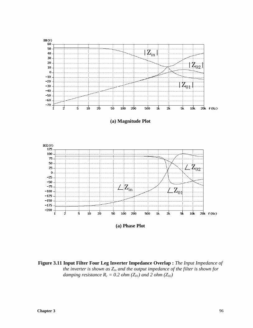
output power. The load is assumed to be resistive. Figure 3.11 shows the impedance overlap
between filter and inverter impedance’s. The plot shows filter input impedance for two values
of damping resistance i.e. Rc = 0.2 ohm & 2 ohm. It can be seen that the impedances do not
overlap and thus there is no interaction problems.
The simulation results are given in Figure 3.12. Figure 3.12 (a) shows the link voltage
after the filter for balanced load of 10 kW. It is maintained constant at 800 V. Figure 3.12 (b)
shows the link voltage for one phase loaded situation. The input current drawn from the DC
link has a 120 Hz component and it results in a 120 Hz ripple (~ 0.2V) on the link voltage as
the input filter is not designed to attenuate low frequency signals.
Chapter 3 96
|Zin|
|Z01|
|Z02|
(a) Magnitude Plot
Zin Z01
Z02
(a) Phase Plot
Figure 3.11 Input Filter Four Leg Inverter Impedance Overlap : The Input Impedance of the inverter is shown as Zin and the output impedance of the filter is shown for damping resistance Rc = 0.2 ohm (Z01) and 2 ohm (Z02)

Chapter 3 97
(a) Balanced Load
(a) Unbalanced Load
Figure 3.12 Link Voltage at the Output of Filter: The filter does not interact with Four Leg Inverter and inverter input voltage is constant in balanced case and has a 120 Hz ripple in unbalanced case.

Chapter 3 98
3.4 PEBB System Level Interaction
This section presents the design and control issues involved with cascading the
converters to form the DC DPS shown in Figure 3.1. Design of intermediate filters and the
effect of filter and subsystems interaction has been discussed in the previous section. When
these converters are cascaded together, possible interaction may occur due to distributed filter
interaction and/or parallel interaction between the load converters. This section investigates
potential interaction problems at interface B, shown in Figure 3.1.
3.4.1 Front End Rectifier and Four Leg Inverter Interface
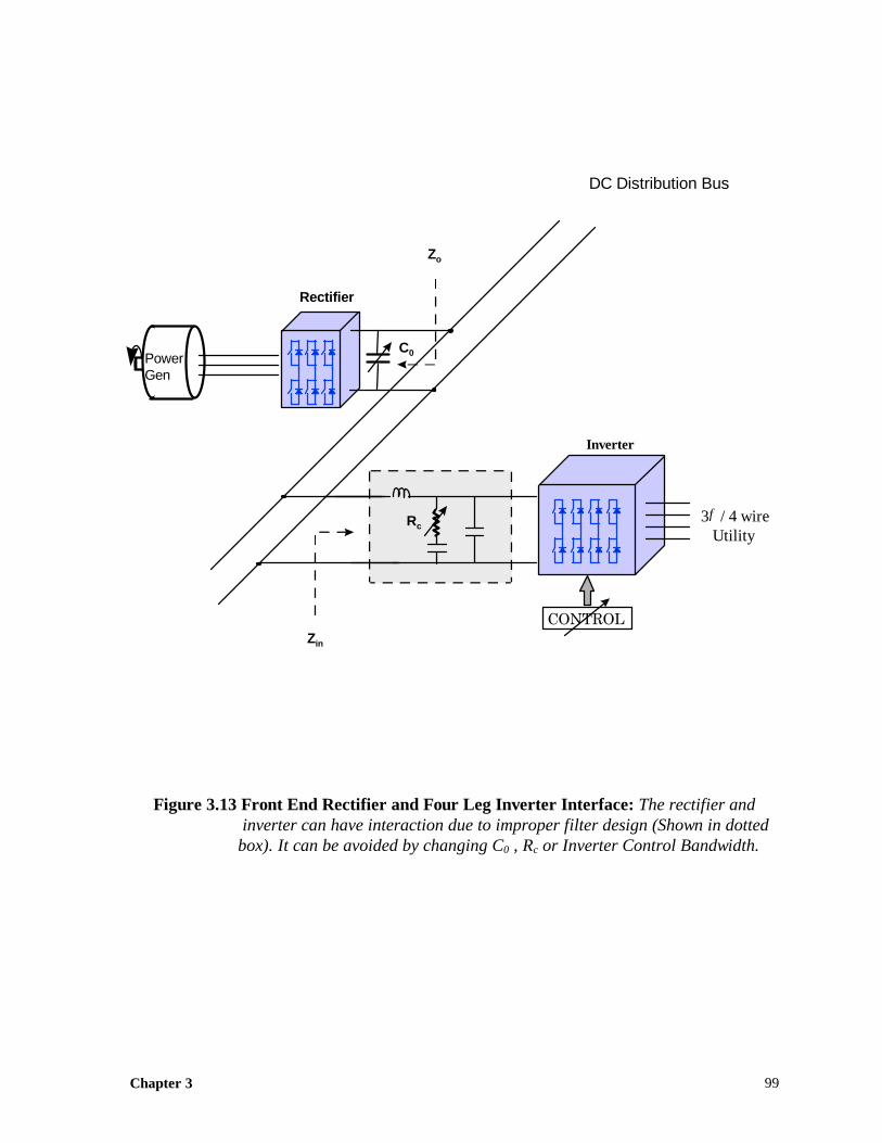
Figure 3.13 shows Boost Rectifier and Four leg Inverter cascaded to form a two
converter subsystem with intermediate filter. The Interface between front end rectifier and the
Four Leg Inverter is checked for system stability. Impedance overlap method is utilized to test
the system stability.
The parameters are given in Appendix A. The output DC link is chosen to be
C0=5 µ F. The damping in the intermediate filter is assumed to be Rc = 0.2 Ω . Figure 3.14
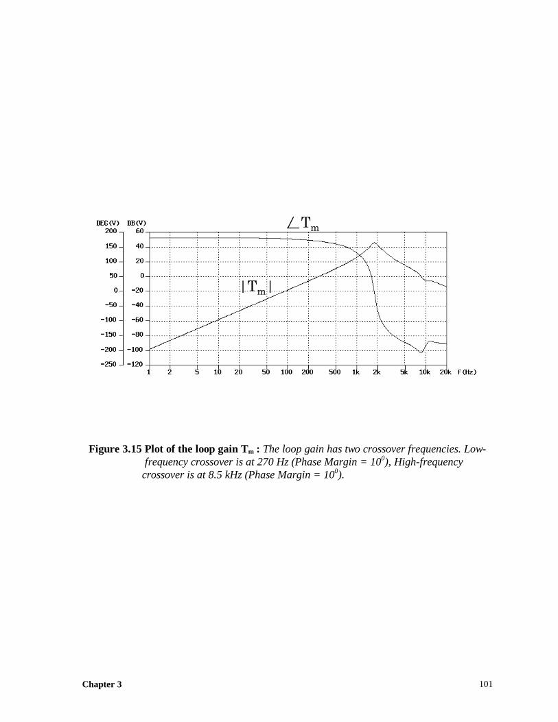
shows the comparison of Z0 and Zin . It is seen that the impedance’s overlap. Figure 3.15
shows the loop gain Tm , and it can be seen that the system has a low phase margin at the two
crossover frequencies ω1 and ω2 .
Chapter 3 99
DC Distribution Bus
Inverter
Power Gen
Rectifier
3 / 4 wire Utility
φ
C0
Zo
Rc
Zin
CONTROL
Figure 3.13 Front End Rectifier and Four Leg Inverter Interface: The rectifier and inverter can have interaction due to improper filter design (Shown in dotted box). It can be avoided by changing C0 , Rc or Inverter Control Bandwidth.

Chapter 3 100
|Zin| |Z0|
(a) Magnitude Plot
Zin
Z0
(b) Phase Plot
Figure 3.14 Rectifier and Inverter Impedance Overlap: When rectifier and inverter are integrated together, their impedance’s interact.
Chapter 3 101
|Tm|
Tm
Figure 3.15 Plot of the loop gain Tm : The loop gain has two crossover frequencies. Low- frequency crossover is at 270 Hz (Phase Margin = 100), High-frequency crossover is at 8.5 kHz (Phase Margin = 100).
Chapter 3 102
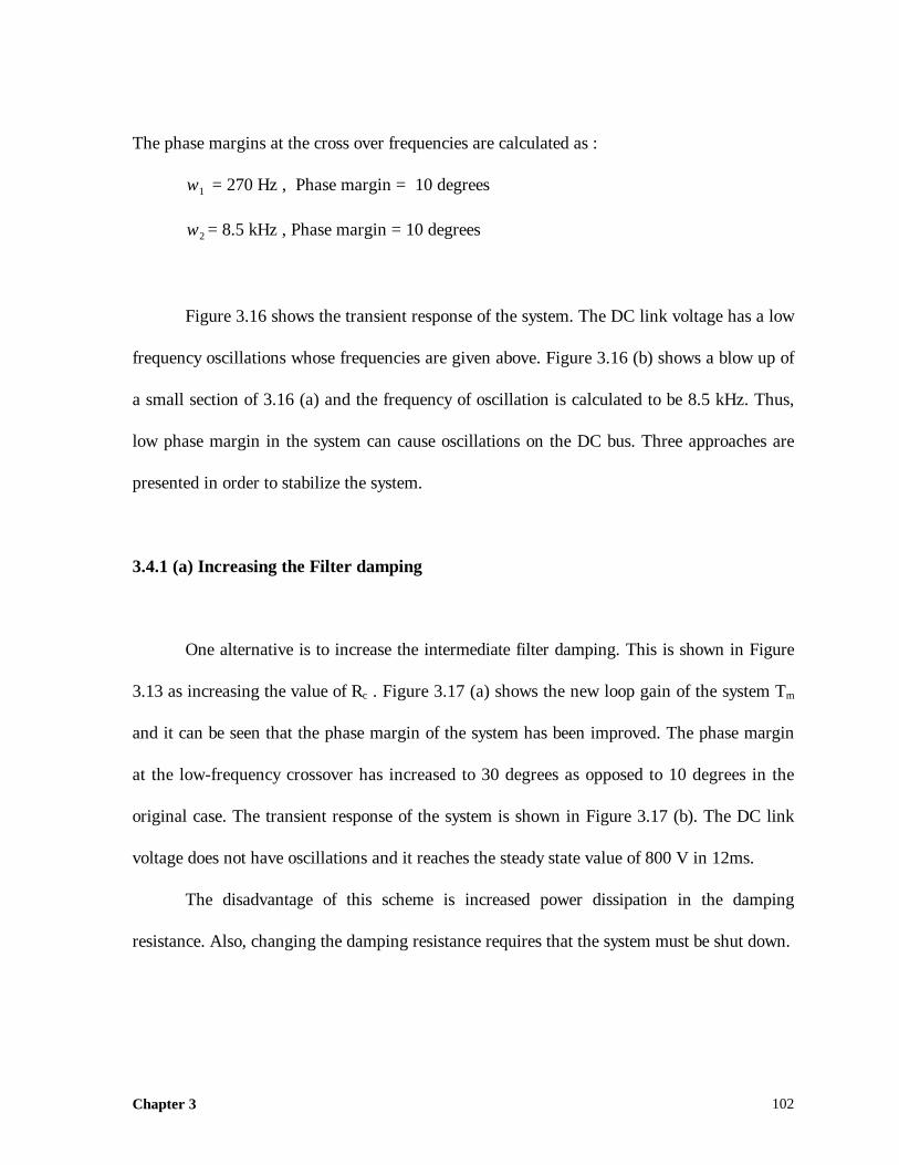
The phase margins at the cross over frequencies are calculated as :
ω1 = 270 Hz , Phase margin = 10 degrees
ω2 = 8.5 kHz , Phase margin = 10 degrees
Figure 3.16 shows the transient response of the system. The DC link voltage has a low
frequency oscillations whose frequencies are given above. Figure 3.16 (b) shows a blow up of
a small section of 3.16 (a) and the frequency of oscillation is calculated to be 8.5 kHz. Thus,
low phase margin in the system can cause oscillations on the DC bus. Three approaches are
presented in order to stabilize the system.
3.4.1 (a) Increasing the Filter damping
One alternative is to increase the intermediate filter damping. This is shown in Figure
3.13 as increasing the value of Rc . Figure 3.17 (a) shows the new loop gain of the system Tm
and it can be seen that the phase margin of the system has been improved. The phase margin
at the low-frequency crossover has increased to 30 degrees as opposed to 10 degrees in the
original case. The transient response of the system is shown in Figure 3.17 (b). The DC link
voltage does not have oscillations and it reaches the steady state value of 800 V in 12ms.
The disadvantage of this scheme is increased power dissipation in the damping
resistance. Also, changing the damping resistance requires that the system must be shut down.

Chapter 3 103
(a) DC Link Voltage
(b) DC link voltage on an expanded time scale
Figure 3.16 Transient Response of Rectifier Inverter Subsystem: The DC link is oscillatory due to low phase margin. It has frequency of oscillation at 270Hz and 8.5 kHz.

Chapter 3 104
(a) DC link transient response
(b) Loop Gain Tm
Figure 3.17 Increasing Damping Resistance : The system can be stabilized by increasing the resistance from 0.2 ohm to 2 ohm.

Chapter 3 105
3.4.1 (b) Increasing the DC link Capacitance
Another alternative is to increase the DC link capacitance. This is shown in Figure
3.13 as increasing the value of C0 . Figure 3.18 (a) shows the new loop gain of the system Tm
and it can be seen that the phase margin of the system has been improved. The transient
response of the system is shown in Figure 3.18 (b). The DC link voltage does not have
oscillations and it reaches the steady state value of 800 V in 50ms.
Thus a small value of output DC link capacitor can cause instability. The capacitor
should be chosen as a large value in order to electrically decouple front end from the load.
But, the drawback of such a approach is large inrush current and poor dynamic response of
the system. Also, as in previous case the system needs to be shut down before any changes
can be made in the DC link capacitance.
3.4.1 (c) Decreasing the Inverter Bandwidth
Another alternative is to decrease the inverter bandwidth. This is shown in Figure 3.13
as changing the inverter controller parameters . Figure 3.19 (b) shows the new loop gain of
the system Tm and it can be seen that the phase margin of the system has been improved. The
low-frequency crossover of the loop gain is 240 Hz and as seen from the Figure 3.19 (b) the
phase margin is 30 degrees.

Chapter 3 106
(a) DC link transient response
(b) Loop Gain Tm
Figure 3.18 Increasing DC link Capacitance : The system is stabilized when the capacitance is increased from 5 uF to 25 uF.

Chapter 3 107
(a) DC link transient response
(b) Loop Gain Tm
Figure 3.19 Reducing Inverter Bandwidth : The system can be stabilized by reducing inverter bandwidth from 2kHz to 10 Hz.

Chapter 3 108
The transient response of the system is shown in Figure 3.19 (a). The DC link voltage does
not have oscillations and it reaches the steady state value of 800 V in 18ms. Decreasing the
inverter bandwidth can be viewed as increasing the system inertia. But, the drawback of such
a approach poor dynamic response of the inverter system. As explained in section 2.4.5,
inverter with low bandwidth cannot take care of unbalanced and non-linear load. However,
this scheme offers the advantage of online control.
The PEBB based system can change the inverter controller parameters and the system
need not be shut down immediately at the cost of poor quality inverter output voltage. But, in
certain applications it may be needed that the system retains power for a short duration before
it is shut down. A PEBB based system offers this flexibility.

Chapter 3 109
3.4.2 DC DPS System Level Interaction
Figure 3.20 shows Boost Rectifier, Four leg Inverter and the DC-DC Converter
cascaded to form the sample DC DPS. Previous section dealt with issues in cascading the
rectifier and the inverter. The rectifier-inverter system is supposed to be stable with the filter
parameters as shown in the Figure 3.20. When the DC-DC converter is integrated with the
rectifier-inverter subsystem to form the DC DPS, possible interactions can occur at the DC
link due to parallel load interaction between the DC-DC converter and the Four Leg Inverter.
Thus, the DC link interface is checked for system stability. Impedance overlap method is
utilized to test the system stability.
The parameters are given in Appendix A. The output DC link is chosen to be
C0=10 µ F. The output power of the rectifier is 20 kW and that of the load converters is 10
kW each. The inverter is supposed to have a large bandwidth i.e. it has 4 zero/5 pole
compensator. The damping in the input filter to the DC-DC converter is assumed to be Rc =
0.2 Ω . Figure 3.21 (a) shows the loop gain Tm , and it can be seen that the system has a low
phase margin at the two crossover frequencies ω1 and ω2 . The phase margins at the cross
over frequencies are calculated as :
ω1 = 120 Hz , Phase margin = 10 degrees
ω2 = 15 kHz , Phase margin = 10 degrees

Chapter 3 110
DC/DC
Inverter
Rectifier
3 φ
C0
Zo
2Zin
CONTROL
Rc
Ω
100µ
µ70
µ22
µ10µ500
µ10
4Ω
VL=200V
VDC=800V
Figure 3.20 DC DPS Interface: The DC DPS may have interaction problems if the DC-DC converter and the inverter have parallel interaction.

Chapter 3 111
(a) Filter Damping Rc = 0.2 ohm
(b) Filter Damping Rc = 2 ohm
Figure 3.21 Loop Gain Tm for different Rc : The loop gain has a low-frequency crossover at 120 Hz (Phase Margin = 10 degrees) in (a) Whereas, has a low-frequency crossover at 140 Hz (Phase Margin = 30 degrees) in (b).

Chapter 3 112
Figure 3.21 (b) shows the loop gain of the system when the damping in the DC-DC
converter input filter is increased from 0.2 ohm to 2 ohm. The low-frequency crossover has
changed to 140 Hz and the phase margin has increased to 30 degrees. Thus the transient
performance is expected to improve.
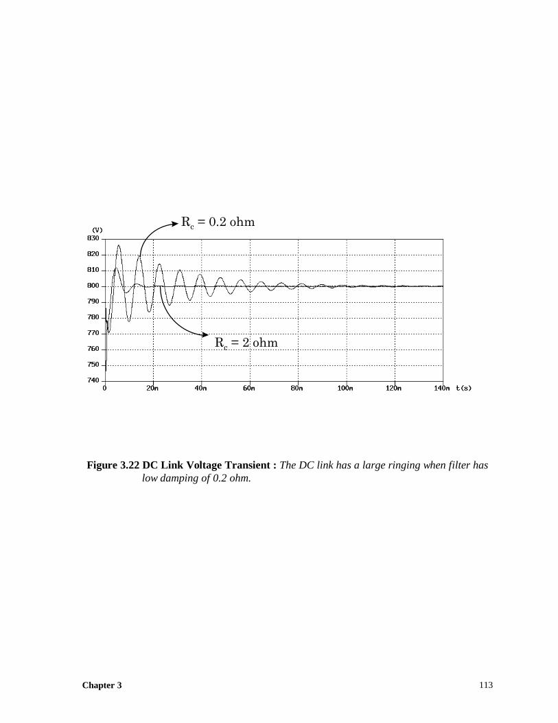
Figure 3.22 shows the transient response of the system. The DC link voltage takes
150ms to settle. The filter damping resistance is increased to Rc = 2 Ω , it is seen that the DC
link voltage reaches steady state in 15ms. Thus, changing the filter dynamics improves the
system response.
Figure 3.23 shows the system response when the inverter is feeding an unbalanced
load. As described in the previous chapter, unbalanced load results in 120Hz current being
drawn from the DC link. As the DC link is not an ideal dc source, as assumed in the previous
chapter, this results in low frequency ringing on the DC link. Figure 3.23 (a) shows the DC
link voltage which has a low frequency component of 120 Hz. The intermediate filter cannot
attenuate the low frequency component. Figure 3.23 (b) shows the d and q axis currents
drawn by the Boost Rectifier. It is seen that they also have a 120 Hz ripple. The d axis current
is responsible for supplying power to the DC bus, and thus it has a large 120 Hz ripple.
Comparing Figures 3.23 (a) and 3.12 (b), it is seen that the link voltage ripple has
increased from 0.2 V to 15 V for the same unbalanced load. This presents a situation when
placing a load in parallel with the inverter leads to parallel load interaction and this results in
increased voltage ripple.
Chapter 3 113
Rc = 0.2 ohm
Rc = 2 ohm
Figure 3.22 DC Link Voltage Transient : The DC link has a large ringing when filter has low damping of 0.2 ohm.

Chapter 3 114
(a) DC Link Voltage
(b) Id and Iq of Boost Rectifier
Figure 3.23 Transient Response of the DC DPS : The DC link voltage has a 120 Hz ripple when the inverter is supplying unbalanced load as shown in (a) and the d axis current in Boost Rectifier also has 120 Hz ripple shown in (b).

Chapter 3 115
3.5 Summary
In this chapter, PEBB system integration issues were discussed. Potential interaction
problems present when integrating the sample DC DPS were studied. The effect of impedance
overlap on the system and individual sub-systems was examined. The ratio of impedances at
the interface between sub-systems was used to determine system stability. Interfaces A,B and
D, as shown in Figure 3.1 were checked for subsystem interaction. It was found that a PEBB
based DC DPS system can assure reliable delivery of electric power to the load, maintain high
system efficiency and flexibility in system operation.
It was found that a lightly damped EMI filter can cause interaction between the filter
and Boost Rectifier. It was shown that a PEBB based rectifier can stabilize the system by
actively doubling the switching frequency and changing the controller parameters, which
resulted in an increase in rectifier bandwidth.
It was shown that problems can occur when separately designed rectifier and inverter
are connected togethar to form the DC DPS. The DC link voltage was found to be oscillatory.
Three methods of avoiding stability problems were outlined namely, increasing the DC link
capacitance, increasing the filter damping and decreasing the load inverter bandwidth. It was
seen that a PEBB based converter has the ability to stabilize the integrated system by actively
changing the inverter bandwidth.
It was shown that when a DC-DC buck converter is added to the DC DPS, possible
interactions can occur. A possible approach to stabilize the DC DPS by changing the damping

Chapter 3 116
in the buck converter input filter was presented. Finally, the PEBB based system was found to
be superior to the conventional system, in terms of performance and system stability.