Embed Size (px)
Citation preview
318
Chapter 13
Noise

319
The news that an Agilent Noise Meas-uring Equipment was to be provided at RAL 2001 in April this year was an opportunity too good to miss. Noise measurement was a thing I had not been involved in and, having by chance just completed a homebrew SLNA preamp for my 10GHz trans-verter, now seemed as good a time to start as any. A quick check of the info around soon revealed the excellent articles by Paul Wade (W1GHZ) previ-ously published in the Microwave Newsletter for November and Decem-ber 1997 but available online www.qsi.net/n1bwt/ noise99.pdf - (Ref. 1). It was decided to build three noise heads using the most likely devices avail-able in the UK and see how well they performed on the day.
Basics The noise head works by using the random noise produced by the ava-lanche breakdown region of a semi-conductor junction. In order to achieve this, a reverse voltage has to be applied to the junction. Clearly the current under these conditions needs to be limited or the junction will be destroyed, and this limiting is achieved by means a series resistor. However the precise current which gives the best noise output at any frequency or the flattest output across all frequencies has to be determined by experiment and there is usually a potentiometer provided for that pur-pose. In choosing a suitable device,
the base-emitter junction of a micro-wave npn device seems to work well although there are advantages in reli-ability and stability in using a specially designed diode such as those pro-duced by Noisecom. These latter de-vices have been designed to minimise flutter effects and instability over time. History With only two weeks to go to the RAL event and other priorities competing, it was decided to buy a selection of likely devices from Farnell and check these out prior to the proper tests at RAL. It was also decided to build a
skeleton assem-bly type source from Paul Wade’s article and also two samples of the later Teflon PCB type using some available Rogers
material. All of them worked but, as luck would have it, the skeleton type proved to have to flattest frequency response from 28MHz to 10GHz. The results are shown below. I must add at this point that these and many other measurements were taken with Ian (G3SEK) operating the controls for much of the day at RAL and it is to Ian and Dave Stockton of Agilent we owe our thanks for the operation and pro-vision of such a great piece of test gear. The noise head had an external 15dB SMA attenuator attached to it throughout the tests and I figured that it would best to keep that attenuator with it.
A Noise Source and its Calibration
David Wrigley, G6GXK
320
Construction: You will almost certainly require some sort of magnifier to assemble this head. I use a headband binocular type, which is “hands free” and doesn’t re-quire the watchmakers ability to screw up the eye to hold an eyeglass. You will need a fairly powerful soldering iron – I used a 40 Watt temperature controlled Weller with a pointed tip. The construction is based on a two hole, female SMA chassis mounting connector. The procedure is as follows: 1. Screw a male connector onto the female connector so that it can be gripped in a vice rear side up. 2. As close as possible to the Teflon form a pool of solder and then drop a 1pF SMD capacitor in it –end on. It will stay that way because of the way the solder surface pulls it. I then tilted the cap towards the central conductor of the connector, because I wanted to make sure that the transistor would fit. Take care only to try to move the ca-pacitor whilst the solder is molten oth-erwise it will fracture near the termina-tion. – (Been there – done that) 3. About a chip length back from the 1pF, mount a 1nF capacitor vertically in another pool of solder. This will be near the fixing hole of the connector – so make sure that it is to one side of it to keep the hole clear. 4. With tweezers carefully mount a 47R (marked 470) SMD resistor across the top of the two capacitors. 5. With tweezers carefully mount the base emitter junction of the BFS520 transistor between the top of the 1pF and the central conductor. If you have done that right , the markings of the transistor will be uppermost and with the collector away from you, the base (LHS) will be connected to the central conductor. 6. Solder a wire near the other side of the Teflon as a ground connection, but don’t thread it through the hole first – unless you are using Teflon insulated
wire. 7. Thread the ground wire through the hole and thread another wire for the supply current through both holes as shown in the photos. This wire can then be soldered to the top of the 1nF where it connects to the 47R. Thread-ing the wires in this way will minimise the possibility of the wire breaking off or worse, pulling off the termination of a component. And that’s it, apart from putting a wire ended 1K fixed resistor (limits the max current) and a 10K pot in series with the live lead, and also not forget-ting to add a BNC connector on the end of the wire, for the supply voltage. Supply voltage differences The supply voltage to the head when driven from the Agilent Equipment is 28 Volts. When I built my PANFI (Precision Automatic Noise Figure Indi-cator) I decided to use 15 Volts, be-cause this was the voltage used by the higher frequency heads manufactured by Noisecom – and one never knows I might be lucky enough to come across one. So I had a noise head calibrated at 28 Volts, with an external series resis-tor of 0.98K + 7.9K (total resistance 0.98K + 7.9K + 47R + 50 R = 8.977, near enough to 9K total) which now needed to have the series resistor changed to enable it to work on 15 Volts. In order to work this out I needed to check the Avalanche break-down voltage at the current at which it was calibrated. So I supplied 28 Volts and measured it – this turned out to be 5.28 Volts (measured across the di-ode), and a calculated current of 2.53mA. The total series resistance required for 15 Volts at 2.53mA is 3.84K. The 47R series resistor and the 50R attenuator input resistance need to be subtracted from this to give the required external resistor 3.74K. A combination of a 3.9K and a 180K in

321
parallel was used to replace the exter-nal resistor and potentiometer. This had the advantage of no potentiometer and therefore no accidental way of it changing.
Conclusions Well, some checks have been made using the head and a home made PANFI (based on ref.1) and now, for the first time, I can see the significant difference in noise figure between a straight FT290 and one with a Mutek front end. There was also found to be a slight benefit in using the Mutek front end in preference to the pre-amp in the 100W PA. I then decided to try the Noise head at 10GHz . Here unfortunately, it dem-onstrated that my attempts at design-ing my own SLNA for 10GHz was less successful than the original G3WDG transverter, which has a NF of be-tween 2 and 3dB. I did try tabbing the lines to improve the matching but try as I could, I could not bring it to the 1dB NF which I believed was possible. I therefore removed the preamp in order to carry out further tests and most probably I will rebuild it later this year.
This noise figure measuring system has certainly proved to be a most use-ful tool and has removed some of guesswork when tuning up receivers. At least I can be confident that I have got my rigs to the best they can do at the time and have revealed the weak-nesses which can be the focus of fu-ture improvement. -----------------------
Ref. 1 - Noise Measurement and gen-eration by Paul Wade (W1GHZ) previ-ously published in the Microwave Newsletter but now available online (www.qsi.net/n1bwt/noise99.pdf ). Ref. 2 - Simple PANFI design – “an Alignment aid” in the Microwave Hand-book, RSGB, 1993 reprint, Vol.2 page 10.37 to 10.42 . It should be noted that some modifications were made to this. 1. The Loudspeaker was omitted from the final build. The LS was found to be acting as a microphone and inputting sound into the system – this gave spurious readings. Therefore an 8 ohm resistor was used instead. 2. The 100uA meter was provided with 8 and 16dB scales and appropriate changes to the series resistors were made. 3. A mains powered +/-17V supply was used to give a regulated 15V for the Head and regulated +/- 12V for the rest of the circuit.
Frequency MHz
Noise Level dB
28 -7.2
50 -6.8
70 -6.7
144 -6.6
432 -6.6
1296 -6.5
2320 -4.0
3450 -9.0
10368 -6.1
322
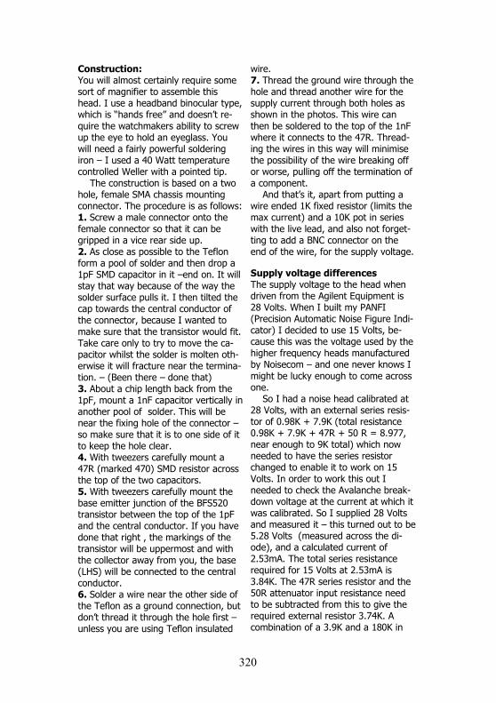
During Our November 2000 San Diego Microwave Group meeting we held a session on noise figure measurement. During problem solving activities in the following weeks, it became obvious that others in our group could make good use of a calibrated noise source. I began looking for an alternative to loaning out the noise source used with my Sanders noise figure meter. I did a quick scan of articles on home brew noise generators and studied in par-ticular Paul Wade's article "Noise: Measurement and Generation" which is available on his website as well as in the ARRL 2nd Microwave Projects Manual. In his excellent article, Paul de-scribes what he went through to build various homebrew noise generators, which included dismantling a commer-cial unit. As soon as I finished the article, an idea hit me that I felt might solve the problems of obtaining high frequency diodes and high quality microwave circuit board material as described in the article. My thought was to use a small section cut from a 14.5GHz upconverter mixer circuit
board used in the early Qualcomm Omnitraks units. This mixer is not useful at 10GHz and is not readily modified to do so but does contain two very good microwave diodes (good through 24GHz) mounted on 15 mil Teflon circuit board The idea was to see how well this mixer diode would perform as a broad-band noise source when operated at the breakdown point with reverse bias. I used Paul's circuit which has the anode of the diode connected directly to the 20dB attenuator. The cathode is RF bypassed to ground and receives bias through a series resistor. Follow-ing Paul's article I found that for the first unit 1.2 milliamps produced the maximum output at 10 GHz so a series resistor was selected (1.6K) to provide 1.2ma with a 12v power supply. Probably the most critical aspect of construction is having as short of paths to ground as possible for the RF bypassing and to the SMA output con-nector. The 0.5 pF capacitor needs to be a good quality microwave type and is removed from another part of the 14.5 GHz mixer board. I made the
Figure1. Circuit Diagram
Low Cost Noise Source for VHF to 10GHz
Based on Qualcomm surplus material
Kerry Banke, N6IZW

323
housing as small as possible to prevent unwanted resonances and also aid in good grounding. The quality of the output attenuator is also a big factor in flatness of frequency response. Half of the battle is building a good noise source & the other half is cali-brating it. The approach I decided to use for calibration over the 145 MHz -10 GHz Ham bands was to use enough broad band amplification ahead of a spectrum analyser (set for 1 dB/div) to provide a Y-Factor of about 3 dB with a source ENR of 5dB (about a 5 dB NF). My setup consisted of two, three stage MMIC amps built by removing the FETs from QC surplus "GOLD Board" LNAs and replacing them with HP MGA-86576 devices. I found that working with two broadband amps with considerable gain creates inter-modulation products from noise when used without a filter between the am-plifiers. For 145 MHz-3456 MHz I was able to use one amplifier without a filter and controlled the gain by vary-ing the power supply voltage. The gain was increased only as needed to get a Y-Factor in the order of at least 3dB. For 5.7 and 10 GHz, a filter was in-serted between the two amplifiers and
the gain again adjusted to the mini-mum capable of doing the job. A goal of 5dB ENR was set as this should be useful for measurement of most pre-amps in the 1- 10 dB NF range. It was found that a total of 23 dB of attenua-tion matched the output of the uncali-brated unit to the calibrated noise source at an arbitrary frequency of 2304 MHz. Other values could certainly be used to match the requirements of particular noise figure measuring units. My experience with the Sanders unit is that it is quite fussy about levels and such and may give erroneous readings unless careful attention is given to the measurement setup. For this reason I tend to use a spectrum analyser or power meter to measure the Y-Factor and calculate the Noise figure. This is not very convenient though when trying to make adjust-ments on the fly but allows measure-ment of most amplifiers and transverters. I generated an Excel spreadsheet (available from Martyn Kinder G0CZD)or http://www.ham-radio.com/sbms/sd/nfcalc2.zip) to aid in calibrating against a known
Figure2. Completed Unit
324
source. The Y-Factor was recorded for both a calibrated source (5 dB ENR) and the uncalibrated unit at each frequency of interest. The Y-Factor values along with the ENR of the calibrated source were entered into the sheet which calculated the ENR of the uncalibrated unit. Other approaches certainly could be used such as using a transverter with the noise sources and measuring the Y-factor at the IF or at the audio output of the IF radio. The results of the first units showed a variation of +/- 1.5 dB over the 50 MHz to 10 GHz range. I believe that with more work the out-put can be made even flatter across the range.
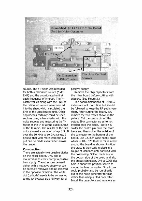
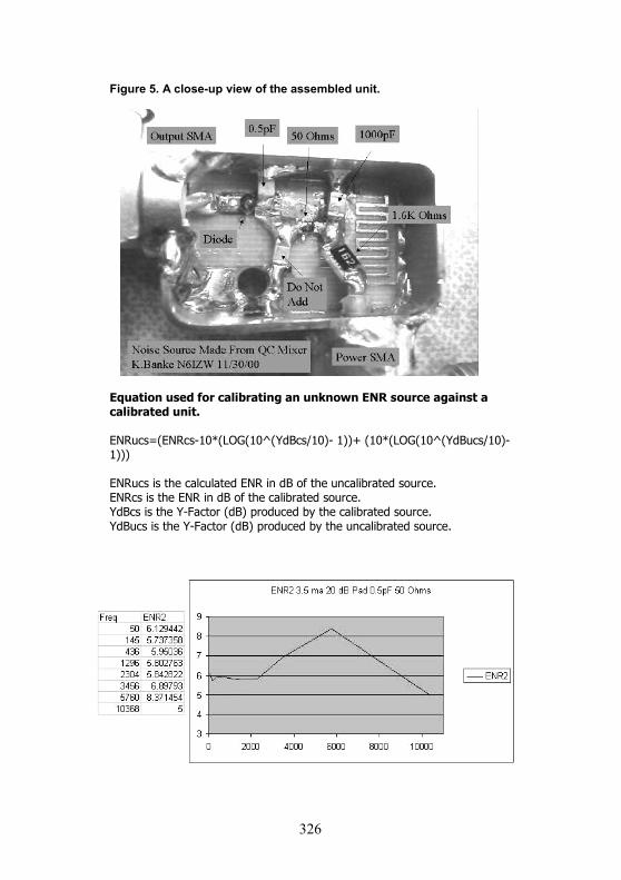
Construction: There are actually two useable diodes on the mixer board. Only one is mounted as to easily accept a positive bias supply. The other can be used either with a negative supply or can be carefully removed and re-soldered in the opposite direction. The white dot (cathode) needs to be connected to the RF bypass/ bias network for a
positive supply. Remove the Chip capacitors from the mixer board before cutting with scissors. (See Figure 3.) The board dimensions of 0.4X0.67 inches are not too critical but should be followed to keep the RF paths very short. After cutting the board, cut/remove the two traces shown in the picture. Cut the centre pin off the output SMA connector so as to not overlap onto the diode. Position & solder the centre pin onto the board trace and then solder the outside of the connector to the bottom of the board. Use 0.5 inch wide hobby brass which is .01-. 025 thick to make a box around the board as shown. Position the brass & then tack in place in a couple of locations until satisfied with the positioning. Solder the brass to the bottom side of the board and also the output connector. Drill a 0.065 dia hole in about the position shown to mount the bias connector. Small coax could probably also be run directly out of the noise generator for bias rather than using a SMA connector. Install the capacitors and resistors as
Figure 3. The Original Board
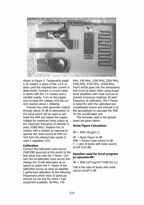
325
shown in Figure 5. Temporarily install a 1K resistor in place of the 1.6 K re-sistor until the required bias current is determined. Connect a current meter in series with the 1-k resistor and a variable supply. Turn on the supply and increase the voltage until the cur-rent reaches about 1 milliamp. Connect the noise generator output through about 25 dB of attenuation to the setup which will be used to cali-brate the ENR and adjust the supply voltage for maximum noise output at the maximum frequency of interest (I used 10368 MHz). Replace the 1k resistor with a resistor as required to operate the noise source at that cur-rent form the desired bias supply (I used a regulated 12V).
Calibration Connect the calibrated noise source (5dB ENR assumed at this point) to the test setup and note the Y-factor. Con-nect the uncalibrated noise source and change the 25-dB attenuator as re-quired to match the Y- Factor of the calibrated source as close as possible. I performed calibration at the following frequencies which were of particular interest for me and for which I had equipment available: 50 MHz, 145
MHz, 436 MHz, 1296 MHz, 2304 MHz, 3456 MHz, 5760 MHz, 10368 MHz. Paul's article goes into the precautions that must be taken when using broad band amplifiers with noise sources to prevent erroneous readings. At each frequency of calibration, the Y-Factor is noted for both the calibrated and uncalibrated source and entered in to the spreadsheet to calculate the ENR for the uncalibrated unit. The formulas used in the spread-sheet are given below:
Noise Figure Calculation NF = ENR-10Log(Y-1)
NF = Noise Figure in dB ENR = Excess noise source in dB Y = ratio of levels with noise source on/off (not dB) Equation used for Excel program to calculate NF:
NF = ENR-(10*Log(10^(YdB/10)-1))
YdB is the ratio of levels with noise source on/off in dB
Figure 4. The board after cutting
326
Equation used for calibrating an unknown ENR source against a calibrated unit. ENRucs=(ENRcs-10*(LOG(10^(YdBcs/10)- 1))+ (10*(LOG(10^(YdBucs/10)-1))) ENRucs is the calculated ENR in dB of the uncalibrated source. ENRcs is the ENR in dB of the calibrated source. YdBcs is the Y-Factor (dB) produced by the calibrated source. YdBucs is the Y-Factor (dB) produced by the uncalibrated source.
Figure 5. A close-up view of the assembled unit.

327
A noise power indicator can be a useful tool for judging the performance of microwave receivers using the Y factor method (cold sky vs. warm object). This relies on the fact that all bodies above absolute zero emit “black body” radiation which can be detected at the higher microwave frequencies. In practice this means that you can use the “cold” sky vs. a known “warm” reference. I find aiming the antenna at the house nearby is best and you can assume its temperature is about 293K. Measurement as opposed to indication can be accomplished by using a preci-sion attenuator in front of the indicator and using the same level at the detec-tor to avoid any non-linearity in the system. I also use my system to ensure that my EME antenna is tracking cor-rectly using moon noise of which I see about 2.5dB at 10GHz. Other uses of this tool can include antenna testing. It provides a more precise and easier to read system than an S-meter and can, in conjunction with a precision attenu-ator provide a means of making fairly precise measurements of the order of +/- 0.2dB. When using a warm source such as your house remember that it should fill the aperture of your antenna. This is why small antennas (more than about 0.5 degrees beam width) do not see the full potential sun or moon noise.
Circuit description (see Figure 1) The system consists of a high gain amplifier ( circa 70dBs) and a sensitive detector at the IF frequency (in this case 144MHz). The bandwidth needs to be as wide as possible but not exceed-ing that of the transverter front end. This is important as noise generated outside the desired pass band of the transverter is not relevant to the sys-
tem performance and could swamp the power indication and lead to mislead-ingly poor indication of receiver per-formance. The 3dB bandwidth of this indicator is about 1MHz. Relative meas-urements are made by using a switched attenuator in front of the noise power indicator. Such attenuators can be found at microwave flea markets. The main challenges to the circuit design and construction are:- 1) minimising the gain required to drive the detector. I.e. the detector must be as sensitive as possible and 2) keeping the gain stages stable at all frequencies including those outside the intended pass band. The first requirement is met by using forward bias on the schottky detector diode to move it into its linear and most sensitive region and by using a simple op-amp to amplify the DC differ-ence between the RF detector and another matched reference diode, simi-larly forward biased but decoupled to RF, in the same SM package. The second requirement is achieved by using MMIC gain stages with careful construction, grounding and shielding. With so much gain on one frequency, great care has to be taken in the layout and construction to avoid instability. The stage before the detector and second band pass filter uses a JFET as this is more tolerant of impedance mismatch. No originality is claimed for any part of the circuit but some time and effort has been spent in trying to ensure the repeatability of the layout and simplicity of the PCB. If good practice for RF construction is followed, it should be possible to build the circuit and get it to be stable quite easily. The input must
A Noise Power Indicator
Brian Coleman. G4NNS
328
however look substantially resistive and be correctly matched at all frequencies. This can be achieved by the use of some fixed attenuation at the input.
Construction (see Figure 2) A simple way to make the PCB is to cover the double sided copper laminate with sticky tape such as 3M Magic tape then stick a print of the track layout onto the tape and use a scalpel or sharp modelling knife to cut out and peel off the areas to be exposed to the etchant. The design uses as many straight lines as possible to simplify this. I found it helpful to use a straight edge under a 3D magnifier. After etching and cleaning the PCB, the screens should be cut to size. The long, side screens are best made using 1/16” laminate as used for the main PCB. The inter stage screens are best made from 1/32” copper laminate or from tin plate. I did not find end screens to be necessary but if you fit them they should be made from 1/16” laminate. Drill 2.5mm holes to recess the MAR8s, which should be the “drop in” type, to minimise lead lengths. Also drill 0.8mm holes for the Via pins. These pins are essential for stability and it is possible that more than the four shown may be needed. (see setting up). As with any PCB construction it is best to start with the smallest compo-nents first as the larger ones will otherwise get in the way (see figures 3 & 4). Whilst the screens should be fitted last you may find it easier to fit L1 and L2 after fitting the long side screen closest to these inductors as this will make it easier to solder the seam. L1 and L2 are separated by about 3mm and are 2-3mm above the ground plane. Note also that the long side screens extend below the main PCB and should match the height of the inter-stage screens on the compo-nent side. They should be soldered both to the top and bottom surfaces of
the main PCB. Make sure the side screens remain at 90 degrees to the PCB by “tack soldering” both sides and repositioning as necessary before sol-dering the entire length of the seams. When assembling the DC amplifier it is again best to fit the smallest compo-nents including the wire links and pins first. I find it best to make the track cuts after the components are in place and to use this process as a check for correct placement of the components. Start fitting the active components with the +5V regulator, and test this before fitting the voltage converter. Test that the + and – 10V rails are working before fitting the op-amp.
Setting up Terminate the input with a good 50 Ohm load. This is essential for stability. Adjust VR1 for zero reading on the meter. If this is not possible the ampli-fier may be oscillating. This should not be happening! If it is try touching dif-ferent gain stages to see if the meter reading changes. You may be able to identify which stage is oscillating by this method. You could try lifting one end of each one Ohm resistor in turn to identify the oscillating stage. Whatever you try, make sure it is reversible and restore it to the original condition be-fore trying something else. Here are some things to try if necessary: 1) Change the capacitor and inductor tuning to see if the oscillation stops. 2) Add additional via pins close to the MAR8s. Those indicated in the design have proved sufficient but in some cases more may be required to achieve stability. 3) Try adjusting the values for R1, R6 or R7 for the stage that is oscillating. Once the amplifier is stable and the meter set to zero, apply a small signal within the pass-band e.g. 144.50MHz from a 50 Ohm source through a switched attenuator. Tune VC1, VC2,
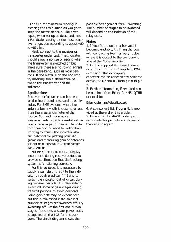
329
L3 and L4 for maximum reading in-creasing the attenuation as you go to keep the meter on scale. The proto-types, when set up as described, had a Full Scale reading on the most sensi-tive range, corresponding to about –80 to –85dBm. Next, connect to the receiver or transverter under test. The Indicator should show a non zero reading when the transverter is switched on but make sure there are no strong signals in the pass-band, such as local bea-cons. If the meter is on the end stop try inserting some attenuation be-tween the transverter and the indicator
Applications Receiver performance can be meas-ured using ground noise and quiet sky noise. For EME systems where the antenna beam width is close to or less than the angular diameter of the source, Sun and moon noise measurements provide a useful indica-tion of receive performance. The indi-cator can also be used for calibration tracking systems. The indicator also has potential for plotting polar dia-grams and measuring gain of antennas for 2m or bands where a transverter has a 2m IF. For EME, the indicator can display moon noise during receive periods to provide confirmation that the tracking system is functioning correctly. For this purpose, it is necessary to supply a sample of the IF to the indi-cator through a splitter ( T ) and to switch the indicator out of circuit dur-ing transmit periods. It is desirable to switch off some of gain stages during transmit periods, to avoid overload. Some gain drift may be experienced but this is minimised if the smallest number of stages are switched off. Try switching off just the first one or two stages if possible. A spare power track is supplied on the PCB for this pur-pose. The circuit diagram shows the
possible arrangement for RF switching. The number of stages to be switched will depend on the isolation of the relay used.
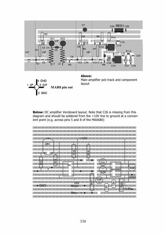
Notes 1. If you fit the unit in a box and it becomes unstable, try lining the box with conducting foam or lossy rubber where it is closest to the component side of the Noise amplifier. 2. On the supplied Veroboard compo-nent layout for the DC amplifier, C26 is missing. This decoupling capacitor can be conveniently soldered across the MX680 IC, from pin 8 to pin 5. 3. Further information, if required can be obtained from Brian, G4NNS, QTHR or email to:
4. A component list, figure 4, is pro-vided at the end of this article. 5. Except for the MAR8 modamps, semiconductor pin outs are shown on the circuit diagram.
330
MAR8 pin out
Below: DC amplifier Veroboard layout. Note that C26 is missing from this diagram and should be soldered from the +10V line to ground at a conven-ient point (e.g. across pins 5 and 8 of the MAX680)
Above: Main amplifier pcb track and component layout
331

332
G4NNS NOISE AMPLIFIER Component List R1 100R Ax C1 1nF SM R2 1R Ax C2 1nF SM R3 51R SMD C3 1nF SM R4 1R Ax C4 100nF SM R5 120R Ax C5 3.3pF Rad R6 1R Ax C6 1nF SM R7 82R Ax C7 10uf Tant R8 100K SM C8 1nF SM R9 2K2 SM C9 100nF SM R10 100R Ax C10 1nF SM R11 10K SM C11 1nF SM R12 10K SM C12 1nF SM R13 1M0 Ax C13 100nF SM R14 1M0 Ax C14 1nF SM VR1 1M C15 100nF SM R15 1M Ax C16 33pf Rad R16 100K Ax C17 2.2pF SM R17 SOT C18 1nF SM C19 33pF Rad VR1 1M0 C20 22pF SM C21 1nF SM
VC122pF C22 1nF SM VC2 22pF C23 1nF SM C24 100nF SM L1 6T 6mm id C25 100nF SM L2 6T 6mm id C26 100nF Rad L3 MC119 1.5T C27 100nF Rad L4 MC119 1.5T C28 100nF Rad C29 100nF Rad C30 4.7 uF C31 4.7 uF C32 4.7 uF C33 4.7 uF Q1 J310 IC4 741 IC5 MAX 680 Farnell 246_451 REG1 7810 REG2 7805 IC1 MAR8 IC2 MAR8 IC3 MAR8 D1-2 BAT 54C Farnell 302_284
333
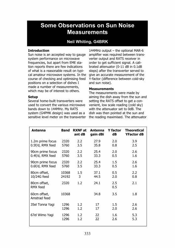
Introduction Sun noise is an accepted way to gauge system performance on microwave frequencies, but apart from EME sta-tion reports there are few indications of what is a reasonable result on typi-cal amateur microwave systems. In the course of checking and optimising feed positions on a selection of dishes I made a number of measurements, which may be of interest to others.
Setup Several home-built transverters were used to convert the various microwave bands down to 144MHz. My RATS system (G4PMK design) was used as a sensitive level meter on the transverter
144MHz output – the optional MAR-6 amplifier was required between trans-verter output and RATS receiver in order to get sufficient signal. A cali-brated attenuator (0-11 dB in 0.1dB steps) after the transverter served to give an accurate measurement of the Y-factor (difference between cold-sky and sun noise).
Measurements The measurements were made by aiming the dish away from the sun and setting the RATS offset to get a con-venient, low scale reading (cold sky) with the attenuator set to 0dB. The dish was then pointed at the sun and the reading maximised. The attenuator
Antenna Band RXNF at ant dB
Antenna gain dBi
Y factor dB
Theoretical YFactor dB
1.2m prime focus 0.5f/d, RMX feed
2320 5760
2.2 3.5
27.9 35.8
2.0 0.8
3.9 2.5
90cm prime focus 0.4f/d, RMX feed
2320 5760
2.2 3.5
25.4 33.3
2.0 0.5
2.6 1.6
90cm prime focus 0.6f/d, RMX feed
2320 5760
2.2 3.5
25.4 33.3
1.5 0.5
2.6 1.6
80cm offset, 10/24G feed
10368 24192
1.5 3
37.1 44.5
0.5 2.0
2.2 0.8
80cm offset, RMX feed
2320 1.2 24.1 2.5 0.5
2.1
60cm offset, Amstrad feed
10368 34.8 3.5 1.8
35el Tonna Yagi 1296 1296
1.2 1.2
17 17
1.5 2.0
2.6 2.6
67el Wimo Yagi 1296 1296
1.2 1.2
22 22
1.6 2.6
5.3 5.3
Some Observations on Sun Noise Measurements
Neil Whiting, G4BRK
334
was then adjusted to give the same reading as the cold sky. The attenua-tion used gives the Y-factor. Antenna gains for the dishes and theoretical Y-Factor come from the Ed Cole (AL7EB) spreadsheet available on the WWW. Dish efficiency of 55% is assumed. For the estimates of 23cm Yagi gains, the Tonna is based on simulation and the Wimo on manufac-turers claims. RX noise figures are estimates.
Conclusions I set out to confirm feed positions for my dishes, and this was successful. It was noted that the deeper dish was more critical on feed position – 10% movement in distance from the dish is quite noticeable in the measurements, though only fractions of a dB. This contrasts with results by others which suggest position needs to be correct to a few mm. I needed 4cm on the 1.2m dish before I could see the Y-factor drop by 0.1dB. The measurements also raise a number of questions, some of which I can attempt to answer: On 2320MHz – why is the 90cm,0.4f/d dish as good as the 1.2m? The WA3RMX feed is designed for deeper dishes, 0.3-0.4f/d, so over-illuminates the 1.2m dish. This adds ground noise from behind the dish to the cold-sky reading and less increase is therefore seen when aiming at the sun. On 5760MHz, why is the 1.2m dish showing an improvement? In this case I can only guess that the RMX feed gives a narrower pattern on 5760 and is relatively better on the shallower dishes. Why is the 60cm dish better than the 80cm dish on 10368MHz? The Amstrad feed on the 60cm is obvi-ously working very well. The 10/24GHz feed on the 80cm uses a piece of 24GHz waveguide let into the back wall of a G4DDK feed. The ‘DDK feed is designed for ~0.5f/d, so will be over-
illuminating the 80cm dish, reducing the Y-factor due to ground noise con-tribution. There may also be a reduc-tion is efficiency due to the 24GHz guide. The 24GHz figure, on the other hand, seems very good – it looks like this feed is accidentally working quite well! How come the 67el Yagi is not much better than the 35el? I don’t know. The difference in claimed gains is ~3dB and the 35el simulates as worse than claimed. There may be a matching difference causing a change in the effective noise figure – I seem to get a higher background noise on the 67el. Some more investigation is required. It is interesting that I see more Y-factor when the antennas are mounted horizontally and moved towards the setting sun. I would have expected less due to part of the beam including the ground and increasing the off-sun background noise. It may be that I am seeing the effect of ground-gain – something that is seen by 2m EME stations. Any other ideas? I learned something from making these meas-urements and can use them in the future to check the effect of improve-ments in each of the systems.