Embed Size (px)
Citation preview

+VS1
VIN
VOUT
–VS1
+VS2
Gnd 2
–VS2
Gnd 1
Product
Folder
Sample &Buy
Technical
Documents
Tools &
Software
Support &Community
ISO124SBOS074D –SEPTEMBER 1997–REVISED JANUARY 2015
ISO124 Precision Lowest-Cost Isolation Amplifier1 Features 3 Description
The ISO124 is a precision isolation amplifier1• 100% Tested for High-Voltage Breakdown
incorporating a novel duty cycle modulation-• Rated 1500 Vrms demodulation technique. The signal is transmitted• High IMR: 140 dB at 60 Hz digitally across a 2-pF differential capacitive barrier.
With digital modulation, the barrier characteristics do• 0.010% Maximum Nonlinearitynot affect signal integrity, thus resulting in excellent• Bipolar Operation: VO = ±10 V reliability and good high-frequency transient immunity
• DIP-16 and SO-28 across the barrier. Both barrier capacitors areimbedded in the plastic body of the package.• Ease of Use: Fixed Unity Gain Configuration
• ±4.5-V to ±18-V Supply Range The ISO124 is easy to use. No external componentsare required for operation. The key specifications are
2 Applications 0.010% maximum nonlinearity, 50-kHz signalbandwidth, and 200-µV/°C VOS drift. A power supply• Industrial Process Control: range of ±4.5 V to ±18 V and quiescent currents of ±5
– Transducer Isolator, Isolator for mA on VS1 and ±5.5 mA on VS2 make the ISO124Thermocouples, RTDs, Pressure Bridges, and ideal for a wide range of applications.Flow Meters, 4-mA to 20-mA Loop Isolation
The ISO124 is available in PDIP-16 and SOIC-28• Ground Loop Elimination plastic surface-mount packages.• Motor and SCR Control
Device Information(1)• Power Monitoring
PART NUMBER PACKAGE BODY SIZE (NOM)• PC-Based Data AcquisitionPDIP (16) 17.90 mm × 7.50 mm• Test Equipment ISO124SOIC (28) 20.01 mm × 6.61 mm
(1) For all available packages, see the orderable addendum atthe end of the data sheet.
4 Simplified Schematic
1
An IMPORTANT NOTICE at the end of this data sheet addresses availability, warranty, changes, use in safety-critical applications,intellectual property matters and other important disclaimers. PRODUCTION DATA.

ISO124SBOS074D –SEPTEMBER 1997–REVISED JANUARY 2015 www.ti.com
Table of Contents8.3 Feature Description................................................... 91 Features .................................................................. 18.4 Device Functional Modes.......................................... 92 Applications ........................................................... 1
9 Application and Implementation ........................ 103 Description ............................................................. 19.1 Application Information............................................ 104 Simplified Schematic............................................. 19.2 Typical Applications ................................................ 115 Revision History..................................................... 2
10 Power Supply Recommendations ..................... 196 Pin Configuration and Functions ......................... 310.1 Signal and Supply Connections ............................ 197 Specifications......................................................... 4
11 Layout................................................................... 207.1 Absolute Maximum Ratings ...................................... 411.1 Layout Guidelines ................................................. 207.2 ESD Ratings.............................................................. 411.2 Layout Example .................................................... 207.3 Recommended Operating Conditions ...................... 4
12 Device and Documentation Support ................. 217.4 Thermal Information .................................................. 412.1 Documentation Support ....................................... 217.5 Electrical Characteristics........................................... 512.2 Trademarks ........................................................... 217.6 Typical Characteristics .............................................. 612.3 Electrostatic Discharge Caution............................ 218 Detailed Description .............................................. 812.4 Glossary ................................................................ 218.1 Overview ................................................................... 8
13 Mechanical, Packaging, and Orderable8.2 Functional Block Diagram ......................................... 8Information ........................................................... 21
5 Revision History
Changes from Revision C (September 2005) to Revision D Page
• Added ESD Ratings table, Feature Description section, Device Functional Modes, Application and Implementationsection, Power Supply Recommendations section, Layout section, Device and Documentation Support section, andMechanical, Packaging, and Orderable Information section. ................................................................................................ 1
2 Submit Documentation Feedback Copyright © 1997–2015, Texas Instruments Incorporated
Product Folder Links: ISO124
1
2
16
15
10
9
7
8
+VS1
–VS1
VOUT
Gnd 2
Gnd 1
VIN
–VS2
+VS2
1
2
28
27
16
15
13
14
+VS1
–VS1
VOUT
Gnd 2
Gnd 1
VIN
–VS2
+VS2
ISO124www.ti.com SBOS074D –SEPTEMBER 1997–REVISED JANUARY 2015
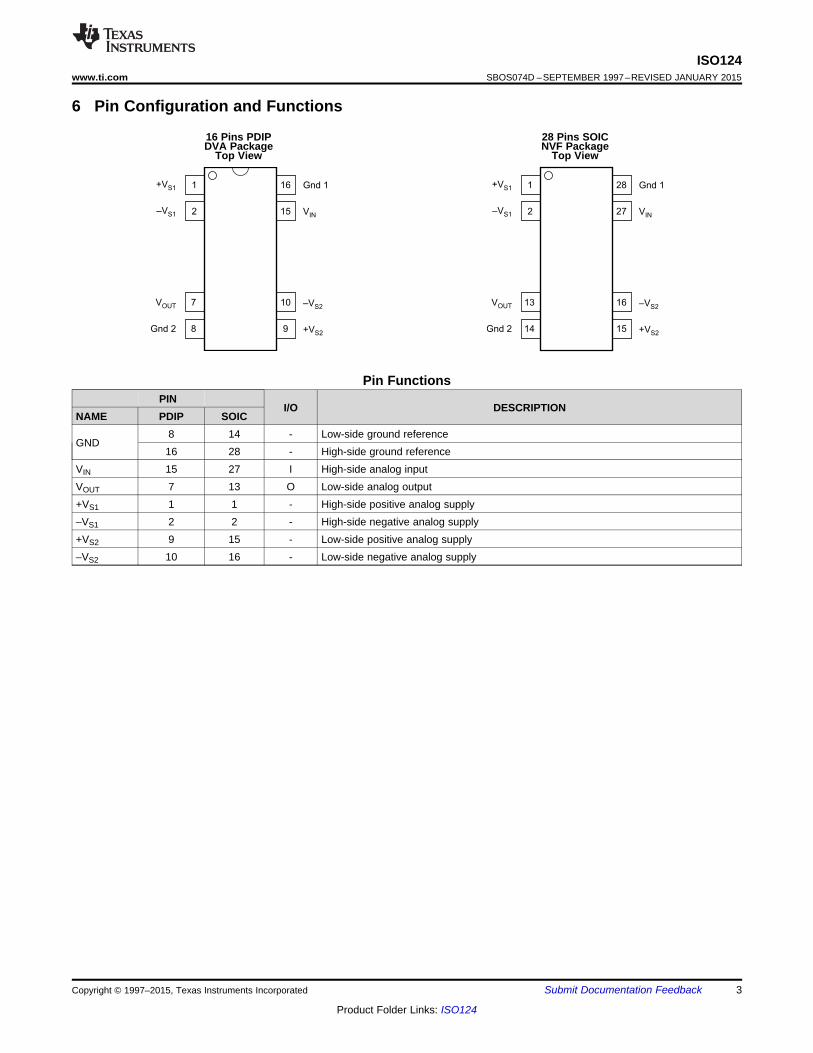
6 Pin Configuration and Functions
16 Pins PDIP 28 Pins SOICDVA Package NVF Package
Top View Top View
Pin FunctionsPIN
I/O DESCRIPTIONNAME PDIP SOIC
8 14 - Low-side ground referenceGND
16 28 - High-side ground referenceVIN 15 27 I High-side analog inputVOUT 7 13 O Low-side analog output+VS1 1 1 - High-side positive analog supply–VS1 2 2 - High-side negative analog supply+VS2 9 15 - Low-side positive analog supply–VS2 10 16 - Low-side negative analog supply
Copyright © 1997–2015, Texas Instruments Incorporated Submit Documentation Feedback 3
Product Folder Links: ISO124

ISO124SBOS074D –SEPTEMBER 1997–REVISED JANUARY 2015 www.ti.com
7 Specifications
7.1 Absolute Maximum Ratingsover operating free-air temperature range (unless otherwise noted) (1)
MIN MAX UNITSupply voltage ±18 VVIN 100 VContinuous isolation voltage 1500 VrmsJunction temperature 125 °COutput short to common ContinuousStorage temperature, Tstg –40 125 °C
(1) Stresses beyond those listed under Absolute Maximum Ratings may cause permanent damage to the device. These are stress ratingsonly, which do not imply functional operation of the device at these or any other conditions beyond those indicated under RecommendedOperating Conditions. Exposure to absolute-maximum-rated conditions for extended periods may affect device reliability.
7.2 ESD RatingsVALUE UNIT
Human body model (HBM), per ANSI/ESDA/JEDEC JS-001 (1) ±1000V(ESD) Electrostatic discharge VCharged-device model (CDM), per JEDEC specification JESD22- ±500
C101 (2)
(1) JEDEC document JEP155 states that 500-V HBM allows safe manufacturing with a standard ESD control process.(2) JEDEC document JEP157 states that 250-V CDM allows safe manufacturing with a standard ESD control process.
7.3 Recommended Operating Conditionsover operating free-air temperature range (unless otherwise noted)
MIN NOM MAX UNITTA –25 85 °CVS1 ±15 VVS2 ±15 VVIN ±10 V
7.4 Thermal InformationISO124
THERMAL METRIC (1) DVA (PDIP) NVF (SOIC) UNIT16 PINS 28 PINS
RθJA Junction-to-ambient thermal resistance 79.8 51.0RθJC(top) Junction-to-case (top) thermal resistance 32.9 32.4RθJB Junction-to-board thermal resistance 42.2 29.5 °C/WψJT Junction-to-top characterization parameter 6.6 10.4ψJB Junction-to-board characterization parameter 40.9 29.0
(1) For more information about traditional and new thermal metrics, see the IC Package Thermal Metrics application report, SPRA953.
4 Submit Documentation Feedback Copyright © 1997–2015, Texas Instruments Incorporated
Product Folder Links: ISO124
ISO124www.ti.com SBOS074D –SEPTEMBER 1997–REVISED JANUARY 2015
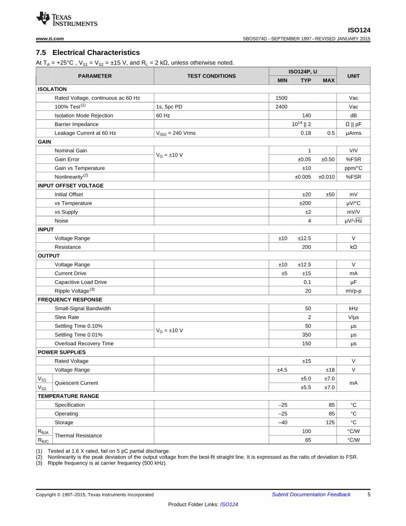
7.5 Electrical CharacteristicsAt TA = +25°C , VS1 = VS2 = ±15 V, and RL = 2 kΩ, unless otherwise noted.
ISO124P, UPARAMETER TEST CONDITIONS UNIT
MIN TYP MAXISOLATION
Rated Voltage, continuous ac 60 Hz 1500 Vac100% Test (1) 1s, 5pc PD 2400 VacIsolation Mode Rejection 60 Hz 140 dBBarrier Impedance 1014 || 2 Ω || pFLeakage Current at 60 Hz VISO = 240 Vrms 0.18 0.5 µArms
GAINNominal Gain 1 V/V
VO = ±10 VGain Error ±0.05 ±0.50 %FSRGain vs Temperature ±10 ppm/°CNonlinearity (2) ±0.005 ±0.010 %FSR
INPUT OFFSET VOLTAGEInitial Offset ±20 ±50 mVvs Temperature ±200 µV/°Cvs Supply ±2 mV/VNoise 4 µV/√Hz
INPUTVoltage Range ±10 ±12.5 VResistance 200 kΩ
OUTPUTVoltage Range ±10 ±12.5 VCurrent Drive ±5 ±15 mACapacitive Load Drive 0.1 µFRipple Voltage (3) 20 mVp-p
FREQUENCY RESPONSESmall-Signal Bandwidth 50 kHzSlew Rate 2 V/µsSettling Time 0.10% 50 µs
VO = ±10 VSettling Time 0.01% 350 µsOverload Recovery Time 150 µs
POWER SUPPLIESRated Voltage ±15 VVoltage Range ±4.5 ±18 V
VS1 ±5.0 ±7.0Quiescent Current mA
VS2 ±5.5 ±7.0TEMPERATURE RANGE
Specification –25 85 °COperating –25 85 °CStorage –40 125 °C
RθJA 100 °C/WThermal Resistance
RθJC 65 °C/W
(1) Tested at 1.6 X rated, fail on 5 pC partial discharge.(2) Nonlinearity is the peak deviation of the output voltage from the best-fit straight line. It is expressed as the ratio of deviation to FSR.(3) Ripple frequency is at carrier frequency (500 kHz).
Copyright © 1997–2015, Texas Instruments Incorporated Submit Documentation Feedback 5
Product Folder Links: ISO124

Frequency (Hz)
IMR
(d
B)
160
140
120
100
80
60
401 10 100 1k 10k 100k 1M
Frequency (Hz)
Peak Isola
tion V
oltage
100 1k 10k 100k 1M 10M 100M
1k
100
0
2.1k
Degraded
Performance
Typical
Performance
Max DC Rating
Time (µs)
+10
0
–10
0 10050
Outp
ut
Voltage
(V)
Time (µs)
+10
0
–10
0 500 1000
Outp
ut
Voltage
(V)
Time (µs)
+10
0
–10
0
Outp
ut
Voltage
(V)
1000500
Time (µs)
+10
0
–10
0 10050
Outp
ut
Voltage
(V)
ISO124SBOS074D –SEPTEMBER 1997–REVISED JANUARY 2015 www.ti.com
7.6 Typical CharacteristicsAt TA = +25°C, and VS = ±15 V, unless otherwise noted.
f = 20 kHzf = 2 kHz
Figure 2. Sine ResponseFigure 1. Sine Response
Figure 3. Step Response Figure 4. Step Response
Figure 5. Isolation Voltage vs Frequency Figure 6. IMR vs Frequency
6 Submit Documentation Feedback Copyright © 1997–2015, Texas Instruments Incorporated
Product Folder Links: ISO124

0
–10
–20
–30
–40
250
200
150
100
50
0 500k 1M 1.5M
Input Frequency (Hz)
VO
UT/V
IN(d
Bm
)
Fre
qu
en
cy O
ut
VOUT/VIN
100kHzFrequency
Out
60
40
20
0
54
1 10 100 1k 10k 100k 1M
Frequency (Hz)
PS
RR
(dB
)
–VS1, –VS2
+VS1, +VS2
100mA
10mA
1mA
100µA
10µA
1µA
0.1µA1 10 100 1k 10k 100k 1M
Frequency (Hz)
Le
aka
ge C
urr
en
t (r
ms)
1500Vrms
240Vrms
ISO124www.ti.com SBOS074D –SEPTEMBER 1997–REVISED JANUARY 2015
Typical Characteristics (continued)At TA = +25°C, and VS = ±15 V, unless otherwise noted.
Figure 7. PSRR vs Frequency Figure 8. Isolation Leakage Current vs Frequency
NOTE: Shaded area shows aliasing frequencies that cannotbe removed by a low-pass filter at the output.
Figure 9. Signal Response to Inputs Greater than 250 kHz
Copyright © 1997–2015, Texas Instruments Incorporated Submit Documentation Feedback 7
Product Folder Links: ISO124

200kΩ
1pF
1pF
1pF
1pF
150pF
Osc
200µA
100µA
Sense
200µA
100µA
200kΩ150pF
S/H
G = 1
S/H
G = 6
Sense
A2
A1
+VS2Gnd 2 –VS2+VS1
Gnd 1 –VS1
VIN
VOUT
Isolation Barrier
ISO124SBOS074D –SEPTEMBER 1997–REVISED JANUARY 2015 www.ti.com
8 Detailed Description
8.1 OverviewThe ISO124 isolation amplifier uses an input and an output section galvanically isolated by matched 1-pFisolating capacitors built into the plastic package. The input is duty-cycle modulated and transmitted digitallyacross the barrier. The output section receives the modulated signal, converts it back to an analog voltage andremoves the ripple component inherent in the demodulation. Input and output sections are fabricated, then lasertrimmed for exceptional circuitry matching common to input and output sections. The sections are then mountedon opposite ends of the package with the isolating capacitors mounted between the two sections. The ISO124contains 250 transistors.
8.1.1 ModuleAn input amplifier (A1, as shown in Functional Block Diagram) integrates the difference between the input current(VIN/200 kΩ) and a switched ±100-µA current source. This current source is implemented by a switchable 200-µAsource and a fixed 100-µA current sink. To understand the basic operation of the modulator, assume that VIN = 0V. The integrator will ramp in one direction until the comparator threshold is exceeded. The comparator andsense amp will force the current source to switch; the resultant signal is a triangular waveform with a 50% dutycycle. The internal oscillator forces the current source to switch at 500 kHz. The resultant capacitor drive is acomplementary duty-cycle modulation square wave
8.1.2 DemodulatorThe sense amplifier detects the signal transitions across the capacitive barrier and drives a switched currentsource into integrator A2. The output stage balances the duty-cycle modulated current against the feedbackcurrent through the 200-kΩ feedback resistor, resulting in an average value at the VOUT pin equal to VIN. Thesample-and-hold amplifiers in the output feedback loop serve to remove undesired ripple voltages inherent in thedemodulation process.
8.2 Functional Block Diagram
8 Submit Documentation Feedback Copyright © 1997–2015, Texas Instruments Incorporated
Product Folder Links: ISO124

ISO124www.ti.com SBOS074D –SEPTEMBER 1997–REVISED JANUARY 2015
8.3 Feature Description
8.3.1 Isolation AmplifierThe ISO124 is a precision analog isolation amplifier. The input signal is transmitted digitally across a high-voltagedifferential capacitive barrier. With digital modulation the barrier characteristics do affect signal integrity, resultingin excellent reliability and high-frequency transient immunity.
8.4 Device Functional ModesThe ISO124 does not have any additional functional modes.
Copyright © 1997–2015, Texas Instruments Incorporated Submit Documentation Feedback 9
Product Folder Links: ISO124

ISO124SBOS074D –SEPTEMBER 1997–REVISED JANUARY 2015 www.ti.com
9 Application and Implementation
NOTEInformation in the following applications sections is not part of the TI componentspecification, and TI does not warrant its accuracy or completeness. TI’s customers areresponsible for determining suitability of components for their purposes. Customers shouldvalidate and test their design implementation to confirm system functionality.
9.1 Application Information
9.1.1 Carrier Frequency ConsiderationsThe ISO124 amplifier transmits the signal across the isolation barrier by a 500-kHz duty-cycle modulationtechnique. For input signals having frequencies below 250 kHz, this system works like any linear amplifier. Butfor frequencies above 250 kHz, the behavior is similar to that of a sampling amplifier. The typical characteristic“Signal Response to Inputs Greater Than 250 kHz” shows this behavior graphically; at input frequencies above250 kHz, the device generates an output signal component of reduced magnitude at a frequency below 250 kHz.This is the aliasing effect of sampling at frequencies less than two times the signal frequency (the Nyquistfrequency). At the carrier frequency and its harmonics, both the frequency and amplitude of the aliasing go tozero.
9.1.2 Isolation Mode Voltage Induced ErrorsIMV can induce errors at the output as indicated by the plots of IMV vs Frequency. It should be noted that if theIMV frequency exceeds 250 kHz, the output also will display spurious outputs (aliasing) in a manner similar tothat for VIN > 250 kHz and the amplifier response will be identical to that shown in the “Signal Response to InputsGreater Than 250 kHz” typical characteristic. This occurs because IMV-induced errors behave like input-referrederror signals. To predict the total error, divide the isolation voltage by the IMR shown in the “IMR versusFrequency” typical performance curve and compute the amplifier response to this input-referred error signal fromthe data given in the “Signal Response to Inputs Greater Than 250 kHz” typical characteristic. For example, if a800-kHz 1000-Vrms IMR is present, then a total of [(–60 dB) + (–30 dB)] x (1000 V) = 32-mV error signal at 200kHz plus a 1-V, 800-kHz error signal will be present at the output.
9.1.3 High IMV dV/dt ErrorsAs the IMV frequency increases and the dV/dt exceeds 1000 Vµs, the sense amp may start to false trigger, andthe output will display spurious errors. The common-mode current being sent across the barrier by the high slewrate is the cause of the false triggering of the sense amplifier. Lowering the power-supply voltages below ±15 Vmay decrease the dV/dt to 500 V/M s for typical performance.
9.1.4 High Voltage TestingTI has adopted a partial discharge test criterion that conforms to the German VDE0884 Optocoupler Standards.This method requires the measurement of minute current pulses (< 5 pC) while applying 2400-Vrms, 60-Hz high-voltage stress across every ISO124 isolation barrier. No partial discharge may be initiated to pass this test. Thiscriterion confirms transient overvoltage (1.6 × 1500 Vrms) protection without damage to the ISO124. Lifetestresults verify the absence of failure under continuous rated voltage and maximum temperature.
This new test method represents the “state-of-the art” for nondestructive high-voltage reliability testing. It isbased on the effects of nonuniform fields that exist in heterogeneous dielectric material during barrierdegradation. In the case of void nonuniformities, electric field stress begins to ionize the void region beforebridging the entire high-voltage barrier. The transient conduction of charge during and after the ionization can bedetected externally as a burst of 0.01–0.1-µs current pulses that repeat on each ac voltage cycle. The minimumac barrier voltage that initiates partial discharge is defined as the “inception voltage.” Decreasing the barriervoltage to a lower level is required before partial discharge ceases and is defined as the “extinction voltage.” Thepackage insulation processes have been characterized and developed to yield an inception voltage in excess of2400 Vrms so that transient overvoltages below this level will not damage the ISO124. The extinction voltage isabove 1500 Vrms so that even overvoltage induced partial discharge will cease once the barrier voltage isreduced to the 1500-Vrms (rated) level. Older high-voltage test methods relied on applying a large enoughovervoltage (above rating) to break down marginal parts, but not so high as to damage good ones. Our newpartial discharge testing gives us more confidence in barrier reliability than breakdown/no breakdown criteria.10 Submit Documentation Feedback Copyright © 1997–2015, Texas Instruments Incorporated
Product Folder Links: ISO124

VIN
VOUT = VIN
Isolation Barrier
ISO124
+VS2
+VS1
–VS1
±VS1
–VS2
Gnd2Gnd1
R1
4.75kΩ
R2
9.76kΩ
1µF 1µF
1µF 1µF
10µH
10µH±VS2
10µH
10µH
1µF 1µF 1µF 1µF
C1
220pF
C2
1000pF
OPA237
ISO124www.ti.com SBOS074D –SEPTEMBER 1997–REVISED JANUARY 2015
9.2 Typical Applications
9.2.1 Output Filters
For more information concerning output filters refer to Application Notes, SBOA012 and SBFA001.
Figure 10. ISO124 With Output Filter for Improved Ripple
9.2.1.1 Design RequirementsThe ISO124 isolation amplifiers (ISO amps) have a small (10 to 20 mVp-p typical) residual demodulator ripple atthe output. A simple filter can be added to eliminate the output ripple without decreasing the 50kHz signalbandwidth of the ISO amp.
9.2.1.2 Detailed Design ProcedureThe ISO124 is designed to have a 50-kHz single-pole (Butterworth) signal response. By cascading the ISO ampwith a simple 50-kHz, Q = 1, two-pole, low-pass filter, the overall signal response becomes three-poleButterworth. The result is a maximally flat 50-kHz magnitude response and the output ripple reduced below thenoise level. Figure 10 shows the complete circuit. The two-pole filter is a unity-gain Sallen-Key type consisting ofA1, R1, R2, C1, and C2. The values shown give Q = 1 and f–3dB bandwidth = 50 kHz. Because the op amp isconnected as a unity-gain follower, gain and gain accuracy of the ISO amp are unaffected. Using a precision opamp such as the OPA602 also preserves the DC accuracy of the ISO amp.
Copyright © 1997–2015, Texas Instruments Incorporated Submit Documentation Feedback 11
Product Folder Links: ISO124

Frequency (Hz)
Ga
in (
dB
)
+3
0
–3
–9
–15
–21
–27
2k 10k 100k 200k
1
2
5k 20k 50k
1) Standard ISO124 has 50kHz single-pole (Butterworth) re-
sponse.
2) ISO124 with cascaded 50kHz, Q = 1, two-pole, low-pass
filter has three-pole Butterworth response.
ISO124SBOS074D –SEPTEMBER 1997–REVISED JANUARY 2015 www.ti.com
Typical Applications (continued)9.2.1.3 Application Curves
Figure 12. Standard ISO124 (Approximately 20-mVp-pFigure 11. Gain vs. FrequencyOutput Ripple)
Figure 13. Filtered ISO124 (No Visible Output Ripple) Figure 14. Step Response of Standard ISO124
Figure 15. Step Response of ISO124 With Added Twopole Figure 16. Large-signal, 10-kHz Sine-wave Response ofOutput Filter ISO124 With and Without Output Filter
12 Submit Documentation Feedback Copyright © 1997–2015, Texas Instruments Incorporated
Product Folder Links: ISO124

15
1
9
10
7
2
e50 = 12V
8
–V16
+V
151
9
10
7
2
10kΩ
8
–V16
+V
10kΩ
e49 = 12V
e2 = 12V
e1 = 12V
10kΩ
10kΩ
Charge/Discharge Control
INA105
25kΩ
25kΩ
25kΩ
25kΩ
2
3
1
e50V =2
+V –V
7 4
5
6
e1V =2
Mu
ltip
lexe
r
Control
Section
ISO124
This Section Repeated 49 Times.
ISO124
ISO124www.ti.com SBOS074D –SEPTEMBER 1997–REVISED JANUARY 2015
Typical Applications (continued)9.2.2 Battery MonitorFigure 17 provides a means to monitor the cell voltage on a 600-V battery stack by using the battery as a powersource for the isolated voltage.
(Derives input power from the battery.)
Figure 17. Battery Monitor for a 600-V Battery Power System
Copyright © 1997–2015, Texas Instruments Incorporated Submit Documentation Feedback 13
Product Folder Links: ISO124

1
2
7
9
10
8
PGA102 ISO124
ISO150
1
2
3
16
4
6
7
85
15 15
+15V– 15V +15V –15V
VIN V
OUT
A
A
0
1
ISO124SBOS074D –SEPTEMBER 1997–REVISED JANUARY 2015 www.ti.com
Typical Applications (continued)9.2.3 Programmable Gain AmplifierIn applications where variable gain configurations are required, a programmable gain amplifier like the PGA102can be used with the ISO124. Figure 18 uses an ISO150 to provide gain pin selection options to the PGA102.
Figure 18. Programmable-Gain Isolation Channel With Gains of 1, 10, and 100
14 Submit Documentation Feedback Copyright © 1997–2015, Texas Instruments Incorporated
Product Folder Links: ISO124

2
610.0V 4REF102
INA114or
INA128
+In7
4
3
8
1
2
5
16
15
8
10
ISO124
7VOUT
96
–In
+15V
+15V
–15V
+15V –15V
ISA
TYPE
E
J
K
T
MATERIAL
Chromel
Constantan
Iron
Constantan
Chromel
Alumel
Copper
Constantan
SEEBACK
COEFFICIENT
(µV/°C)
58.5
50.2
39.4
38.0
R2
(R3 = 100Ω)
3.48kΩ
4.12kΩ
5.23kΩ
5.49kΩ
R4
(R5 + R6 = 100Ω)
56.2kΩ
64.9kΩ
80.6kΩ
84.5kΩ
+15V –15V
R3
100Ω
Ground Loop Through Conduit
NOTE: (1) –2.1mV/°C at 2.00µA.
R1
27kΩ
Isothermal
Block with
1N4148(1)
R21MΩ
R5
50Ω
RG
R4
R6 100
Zero Adj
Thermocouple
21
ISO124www.ti.com SBOS074D –SEPTEMBER 1997–REVISED JANUARY 2015
Typical Applications (continued)9.2.4 Thermocouple AmplifierFor isolated temperature measurements, Figure 19 provides an application solution using the INA114 or INA128feeding the input stage of the ISO124. The table provides suggested resistor values based on the type ofthermistor used in the application.
Figure 19. Thermocouple Amplifier With Ground Loop Elimination,Cold Junction Compensation, and Up-scale Burn-out
Copyright © 1997–2015, Texas Instruments Incorporated Submit Documentation Feedback 15
Product Folder Links: ISO124

R1 R2
R4
INA105
Difference Amp
R3
RS
2
3
4
IN4689
5.1V
Reference
5
7
6
1VIN
Signal Source
+
10kΩ
15
–VS2 (–15V)
+VS2 (+15V)
VS1 (+15V)
16
–VS1
Com 210
In
GndRC
(1)
VS
(V)
20+
15
12
INPUT RANGE
(V)(1)
–2 to +10
–2 to +5
–2 to +2
7
9
8
ISO124
2
1
VOUT = VIN
RCM
1kΩ
RCV420
XTR105RG
RZ(1)
13
3
4
26
7
10141
0.01µF
4-20mA
RTD
(PT100)
0.8mA 0.8mA
1.6mA
1415
16
3
2
10 4
12
11
5, 13
15
16
2
1
Gnd
–VS = –15V
on PWS740
+VS = 15V on PWS740
9
10
7
8
–V
+V
ISO124
VOUT
0V - 5V
ISO124SBOS074D –SEPTEMBER 1997–REVISED JANUARY 2015 www.ti.com
Typical Applications (continued)9.2.5 Isolated 4- to 20-mA Instrument LoopFor isolated temperature measurements in a 4- to 20-mA loop, Figure 20 provides a solution using the XTR101and RCV420. A high-performance PT100 resistance temperature detector (RTD) provides the user with anisolated 0- to 5-V representation of the isolated temperature measurement.
Figure 20. Isolated 4- to 20-mA Instrument Loop (RTD Shown)
9.2.6 Single-Supply Operation of the ISO124 Isolation AmplifierThe circuit shown in Figure 21 uses a 5.1-V Zener diode to generate the negative supply for an ISO12x from asingle supply on the high-voltage side of the isolation amplifier. The input measuring range will be dependent onthe applied voltage as noted in the accompanying table.
NOTE: Because the amplifier is unity gain, the input range is also the output range. The output can go to –2 V because theoutput section of the ISO amp operates from dual supplies.For additional information refer to Application Note SBOA004
Figure 21. Single-Supply Operation of the ISO124 Isolation Amplifier Schematic
16 Submit Documentation Feedback Copyright © 1997–2015, Texas Instruments Incorporated
Product Folder Links: ISO124

16
Gnd VIN V– V+
V+ V– VO Gnd
15
1 2
1 2
10 9
7 8
Input
Section
Output
Section
5 6 7
VIN
InputGnd
+15V
–15V
–15V, 20mA
+15V, 20mA
AuxiliaryIsolatedPowerOutput
OutputGnd
VO
ISO124
0.47µF
0.47µF
0.47µF
DCP011515DB
or
DCV011515D
ISO124www.ti.com SBOS074D –SEPTEMBER 1997–REVISED JANUARY 2015
Typical Applications (continued)9.2.7 Input-Side Powered ISO AmplifierThe user side of the ISO124 can be powered from the high voltage side using an isolated DC-DC converter asshown in Figure 22.
Figure 22. Input-Side Powered ISO Amplifier Schematic
Copyright © 1997–2015, Texas Instruments Incorporated Submit Documentation Feedback 17
Product Folder Links: ISO124

16
Gnd VIN V– V+
V+ V– VO Gnd
15
1 2
1 2
10 9
7 8
Input
Section
Output
Section
5 6 7
+15V Gnd
7 6 5 2 1
VIN
InputGnd
+15V, 20mA
–15V, 20mA
–15V, 20mA
+15V, 20mA
AuxiliaryIsolatedPowerOutput
AuxiliaryIsolatedPowerOutput
OutputGnd
VO
ISO124
0.47µF
0.47µF
0.47µF
0.47µF 0.47µF
DCP011515DB
or
DCV011515D
DCP011515DB
or
DCV011515D
ISO124SBOS074D –SEPTEMBER 1997–REVISED JANUARY 2015 www.ti.com
Typical Applications (continued)9.2.8 Powered ISO Amplifier With Three-Port IsolationFigure 23 illustrates an application solution that provides isolated power to both the user and high-voltage sidesof the ISO124 amplifier.
Figure 23. Powered ISO Amplifier With Three-Port Isolation Schematic
18 Submit Documentation Feedback Copyright © 1997–2015, Texas Instruments Incorporated
Product Folder Links: ISO124

+VS1
+VS2
GndGnd
VINVOUT
–VS1
±VS1 ±VS2
–VS2
1µF 1µF 1µF 1µF
Isolation Barrier
ISO124
ISO124www.ti.com SBOS074D –SEPTEMBER 1997–REVISED JANUARY 2015
10 Power Supply Recommendations
10.1 Signal and Supply ConnectionsEach power-supply pin should be bypassed with 1-µF tantalum capacitors located as close to the amplifier aspossible. The internal frequency of the modulator/demodulator is set at 500 kHz by an internal oscillator.Therefore, if it is desired to minimize any feedthrough noise (beat frequencies) from a DC-DC converter, use a πfilter on the supplies (see Figure 10). The ISO124 output has a 500-kHz ripple of 20 mV, which can be removedwith a simple 2-pole low-pass filter with a 100-kHz cutoff using a low-cost op amp (see Figure 10).
The input to the modulator is a current (set by the 200-kΩ integrator input resistor) that makes it possible to havean input voltage greater than the input supplies, as long as the output supply is at least ±15 V. It is thereforepossible, when using an unregulated DC-DC converter, to minimize PSR related output errors with ±5-V voltageregulators on the isolated side and still get the full ±10-V input and output swing.
Figure 24. Basic Signal and Power Connections
Copyright © 1997–2015, Texas Instruments Incorporated Submit Documentation Feedback 19
Product Folder Links: ISO124

ISO124
GND +VS2
1
Top View
LEGEND
TOP layer: copper pour & traces
GND
via to ground plane
-VS2
VIN
VOUT
GND
1 µF
SMD0603
1 µF
SMD0603
-VS1
+VS1
1 µF
SMD0603
1 µF
SMD0603
ISOLATION BOUNDARY
ISOLATION BOUNDARY
ISO124SBOS074D –SEPTEMBER 1997–REVISED JANUARY 2015 www.ti.com
11 Layout
11.1 Layout GuidelinesTo maintain the isolation barrier of the device, the distance between the high-side ground (pin 16 or 28) and thelow-side ground (pin 8 or 14) should be kept at maximum; that is, the entire area underneath the device shouldbe kept free of any conducting materials.
11.2 Layout Example
Figure 25. ISO124 Layout Example
20 Submit Documentation Feedback Copyright © 1997–2015, Texas Instruments Incorporated
Product Folder Links: ISO124

ISO124www.ti.com SBOS074D –SEPTEMBER 1997–REVISED JANUARY 2015
12 Device and Documentation Support
12.1 Documentation Support
12.1.1 Related Documentation• Single-Supply Operation of Isolation Amplifiers, SBOA004• Simple Output Filter Eliminates ISO Amp Output Ripple and Keeps Full Bandwidth, SBOA012• FilterPro™ User's Guide, SBFA001
12.2 TrademarksFilterPro is a trademark of Texas Instruments.All other trademarks are the property of their respective owners.
12.3 Electrostatic Discharge CautionThese devices have limited built-in ESD protection. The leads should be shorted together or the device placed in conductive foamduring storage or handling to prevent electrostatic damage to the MOS gates.
12.4 GlossarySLYZ022 — TI Glossary.
This glossary lists and explains terms, acronyms, and definitions.
13 Mechanical, Packaging, and Orderable InformationThe following pages include mechanical, packaging, and orderable information. This information is the mostcurrent data available for the designated devices. This data is subject to change without notice and revision ofthis document. For browser-based versions of this data sheet, refer to the left-hand navigation.
Copyright © 1997–2015, Texas Instruments Incorporated Submit Documentation Feedback 21
Product Folder Links: ISO124

PACKAGE OPTION ADDENDUM
www.ti.com 10-Sep-2014
Addendum-Page 1
PACKAGING INFORMATION
Orderable Device Status(1)
Package Type PackageDrawing
Pins PackageQty
Eco Plan(2)
Lead/Ball Finish(6)
MSL Peak Temp(3)
Op Temp (°C) Device Marking(4/5)
Samples
ISO124P ACTIVE PDIP NVF 8 25 Pb-Free(RoHS)
CU NIPDAU N / A for Pkg Type -25 to 85 ISO124P
ISO124U ACTIVE SOIC DVA 8 20 Green (RoHS& no Sb/Br)
CU NIPDAU Level-3-260C-168 HR -25 to 85 ISO124U
ISO124U/1K ACTIVE SOIC DVA 8 1000 Green (RoHS& no Sb/Br)
CU NIPDAU Level-3-260C-168 HR -25 to 85 ISO124U
ISO124U/1KE4 ACTIVE SOIC DVA 8 1000 Green (RoHS& no Sb/Br)
CU NIPDAU Level-3-260C-168 HR -25 to 85 ISO124U
ISO124UE4 ACTIVE SOIC DVA 8 20 Green (RoHS& no Sb/Br)
CU NIPDAU Level-3-260C-168 HR -25 to 85 ISO124U
(1) The marketing status values are defined as follows:ACTIVE: Product device recommended for new designs.LIFEBUY: TI has announced that the device will be discontinued, and a lifetime-buy period is in effect.NRND: Not recommended for new designs. Device is in production to support existing customers, but TI does not recommend using this part in a new design.PREVIEW: Device has been announced but is not in production. Samples may or may not be available.OBSOLETE: TI has discontinued the production of the device.
(2) Eco Plan - The planned eco-friendly classification: Pb-Free (RoHS), Pb-Free (RoHS Exempt), or Green (RoHS & no Sb/Br) - please check http://www.ti.com/productcontent for the latest availabilityinformation and additional product content details.TBD: The Pb-Free/Green conversion plan has not been defined.Pb-Free (RoHS): TI's terms "Lead-Free" or "Pb-Free" mean semiconductor products that are compatible with the current RoHS requirements for all 6 substances, including the requirement thatlead not exceed 0.1% by weight in homogeneous materials. Where designed to be soldered at high temperatures, TI Pb-Free products are suitable for use in specified lead-free processes.Pb-Free (RoHS Exempt): This component has a RoHS exemption for either 1) lead-based flip-chip solder bumps used between the die and package, or 2) lead-based die adhesive used betweenthe die and leadframe. The component is otherwise considered Pb-Free (RoHS compatible) as defined above.Green (RoHS & no Sb/Br): TI defines "Green" to mean Pb-Free (RoHS compatible), and free of Bromine (Br) and Antimony (Sb) based flame retardants (Br or Sb do not exceed 0.1% by weightin homogeneous material)
(3) MSL, Peak Temp. - The Moisture Sensitivity Level rating according to the JEDEC industry standard classifications, and peak solder temperature.
(4) There may be additional marking, which relates to the logo, the lot trace code information, or the environmental category on the device.
(5) Multiple Device Markings will be inside parentheses. Only one Device Marking contained in parentheses and separated by a "~" will appear on a device. If a line is indented then it is a continuationof the previous line and the two combined represent the entire Device Marking for that device.

PACKAGE OPTION ADDENDUM
www.ti.com 10-Sep-2014
Addendum-Page 2
(6) Lead/Ball Finish - Orderable Devices may have multiple material finish options. Finish options are separated by a vertical ruled line. Lead/Ball Finish values may wrap to two lines if the finishvalue exceeds the maximum column width.
Important Information and Disclaimer:The information provided on this page represents TI's knowledge and belief as of the date that it is provided. TI bases its knowledge and belief on informationprovided by third parties, and makes no representation or warranty as to the accuracy of such information. Efforts are underway to better integrate information from third parties. TI has taken andcontinues to take reasonable steps to provide representative and accurate information but may not have conducted destructive testing or chemical analysis on incoming materials and chemicals.TI and TI suppliers consider certain information to be proprietary, and thus CAS numbers and other limited information may not be available for release.
In no event shall TI's liability arising out of such information exceed the total purchase price of the TI part(s) at issue in this document sold by TI to Customer on an annual basis.

TAPE AND REEL INFORMATION
*All dimensions are nominal
Device PackageType
PackageDrawing
Pins SPQ ReelDiameter
(mm)
ReelWidth
W1 (mm)
A0(mm)
B0(mm)
K0(mm)
P1(mm)
W(mm)
Pin1Quadrant
ISO124U/1K SOIC DVA 8 1000 330.0 24.4 10.9 18.3 3.2 12.0 24.0 Q1
PACKAGE MATERIALS INFORMATION
www.ti.com 10-Sep-2014
Pack Materials-Page 1

*All dimensions are nominal
Device Package Type Package Drawing Pins SPQ Length (mm) Width (mm) Height (mm)
ISO124U/1K SOIC DVA 8 1000 367.0 367.0 45.0
PACKAGE MATERIALS INFORMATION
www.ti.com 10-Sep-2014
Pack Materials-Page 2

MECHANICAL DATA
MPDI072 – AUGUST 2001
1POST OFFICE BOX 655303 • DALLAS, TEXAS 75265
NVF (R-PDIP-T8/16) PLASTIC DUAL-IN-LINE
4202501/A 08/01
0.150 (3,81)0.115 (2,92)
C
0.005 (0,13)MIN 4 PL
1 8
916
0.775 (21,34)0.735 (18,67)
0.240 (6,10)0.280 (7,11)
0.070 (1,78)0.045 (1,14)0.030 (0,76)
0.045 (1,14)
0.014 (0,36)0.022 (0,56)
0.010 (0,25) M C
0.210 (5,33)
0.195 (4,95)0.115 (2,92)
0.300 (7,63)
MAX0.430 (10,92)
0.000 (0,00)0.060 (1,52)
0.014 (0,36)0.008 (0,20)
0.325 (8,26)0.300 (7,62)
IndexArea
0.015 (0,38)MIN
0.100 (2,54)
Seating PlaneBase Plane
MAX
F
F
D
D
D
E
1/2 Lead
A. All linear dimensions are in inches (millimeters).B. This drawing is subject to change without notice.
C. Falls within JEDEC MS-001-BB with the exception of leadcount.
D. Dimensions do not include mold flash or protrusions.Mold flash or protrusions shall not exceed 0.010 (0,25).
E. Dimensions measured with the leads constrained to beperpendicular to Datum C.
F. Dimensions are measured at the lead tips with the leadsunconstrained.
G. A visual index feature must be located within thecross-hatched area.

MECHANICAL DATA
MPDS105 – AUGUST 2001
1POST OFFICE BOX 655303 • DALLAS, TEXAS 75265
DVA (R-PDSO-G8/28) PLASTIC SMALL-OUTLINE
4202103/B 08/01
IndexArea
1 14
1528
SeatingPlane
17,7018,10
7,607,40 10,01
10,65
2,352,65
0,300,10
0,510,33
0,320,23
0,250,75
x 45°
1,270,40
0°–8°
C
F
G1,27
0,25 M BAC S
0,10
0,25 MB
C
B
A
D
M
M
NOTES: A. All linear dimensions are in millimeters.B. This drawing is subject to change without notice.
C. Body length dimension does not include moldflash, protrusions, or gate burrs. Mold flash, protrusions,and gate burrs shall not exceed 0,15 mm per side.
D. Body width dimension does not include inter-lead flashor portrusions. Inter-lead flash and protrusionsshall not exceed 0,25 mm per side.
E. The chamfer on the body is optional. If it is not present,a visual index feature must be located within thecross-hatched area.
F. Lead dimension is the length of terminal for solderingto a substrate.
G. Lead width, as measured 0,36 mm or greaterabove the seating plane, shall not exceed amaximum value of 0,61 mm.
H. Lead-to-lead coplanarity shall be less than0,10 mm from seating plane.
I. Falls within JEDEC MS-013-AE with the exceptionof the number of leads.

IMPORTANT NOTICE
Texas Instruments Incorporated and its subsidiaries (TI) reserve the right to make corrections, enhancements, improvements and otherchanges to its semiconductor products and services per JESD46, latest issue, and to discontinue any product or service per JESD48, latestissue. Buyers should obtain the latest relevant information before placing orders and should verify that such information is current andcomplete. All semiconductor products (also referred to herein as “components”) are sold subject to TI’s terms and conditions of salesupplied at the time of order acknowledgment.TI warrants performance of its components to the specifications applicable at the time of sale, in accordance with the warranty in TI’s termsand conditions of sale of semiconductor products. Testing and other quality control techniques are used to the extent TI deems necessaryto support this warranty. Except where mandated by applicable law, testing of all parameters of each component is not necessarilyperformed.TI assumes no liability for applications assistance or the design of Buyers’ products. Buyers are responsible for their products andapplications using TI components. To minimize the risks associated with Buyers’ products and applications, Buyers should provideadequate design and operating safeguards.TI does not warrant or represent that any license, either express or implied, is granted under any patent right, copyright, mask work right, orother intellectual property right relating to any combination, machine, or process in which TI components or services are used. Informationpublished by TI regarding third-party products or services does not constitute a license to use such products or services or a warranty orendorsement thereof. Use of such information may require a license from a third party under the patents or other intellectual property of thethird party, or a license from TI under the patents or other intellectual property of TI.Reproduction of significant portions of TI information in TI data books or data sheets is permissible only if reproduction is without alterationand is accompanied by all associated warranties, conditions, limitations, and notices. TI is not responsible or liable for such altereddocumentation. Information of third parties may be subject to additional restrictions.Resale of TI components or services with statements different from or beyond the parameters stated by TI for that component or servicevoids all express and any implied warranties for the associated TI component or service and is an unfair and deceptive business practice.TI is not responsible or liable for any such statements.Buyer acknowledges and agrees that it is solely responsible for compliance with all legal, regulatory and safety-related requirementsconcerning its products, and any use of TI components in its applications, notwithstanding any applications-related information or supportthat may be provided by TI. Buyer represents and agrees that it has all the necessary expertise to create and implement safeguards whichanticipate dangerous consequences of failures, monitor failures and their consequences, lessen the likelihood of failures that might causeharm and take appropriate remedial actions. Buyer will fully indemnify TI and its representatives against any damages arising out of the useof any TI components in safety-critical applications.In some cases, TI components may be promoted specifically to facilitate safety-related applications. With such components, TI’s goal is tohelp enable customers to design and create their own end-product solutions that meet applicable functional safety standards andrequirements. Nonetheless, such components are subject to these terms.No TI components are authorized for use in FDA Class III (or similar life-critical medical equipment) unless authorized officers of the partieshave executed a special agreement specifically governing such use.Only those TI components which TI has specifically designated as military grade or “enhanced plastic” are designed and intended for use inmilitary/aerospace applications or environments. Buyer acknowledges and agrees that any military or aerospace use of TI componentswhich have not been so designated is solely at the Buyer's risk, and that Buyer is solely responsible for compliance with all legal andregulatory requirements in connection with such use.TI has specifically designated certain components as meeting ISO/TS16949 requirements, mainly for automotive use. In any case of use ofnon-designated products, TI will not be responsible for any failure to meet ISO/TS16949.
Products ApplicationsAudio www.ti.com/audio Automotive and Transportation www.ti.com/automotiveAmplifiers amplifier.ti.com Communications and Telecom www.ti.com/communicationsData Converters dataconverter.ti.com Computers and Peripherals www.ti.com/computersDLP® Products www.dlp.com Consumer Electronics www.ti.com/consumer-appsDSP dsp.ti.com Energy and Lighting www.ti.com/energyClocks and Timers www.ti.com/clocks Industrial www.ti.com/industrialInterface interface.ti.com Medical www.ti.com/medicalLogic logic.ti.com Security www.ti.com/securityPower Mgmt power.ti.com Space, Avionics and Defense www.ti.com/space-avionics-defenseMicrocontrollers microcontroller.ti.com Video and Imaging www.ti.com/videoRFID www.ti-rfid.comOMAP Applications Processors www.ti.com/omap TI E2E Community e2e.ti.comWireless Connectivity www.ti.com/wirelessconnectivity
Mailing Address: Texas Instruments, Post Office Box 655303, Dallas, Texas 75265Copyright © 2015, Texas Instruments Incorporated