Embed Size (px)
Citation preview


Challenges in Silicon Photonics WDM Technology
Yung-Jr Hung, Professor
Department of Photonics, National Sun Yat-sen University

Outline
Motivations
Fabrication-tolerant MZI design
Cascaded MZIs for WDM (de)multiplexers
Conclusions
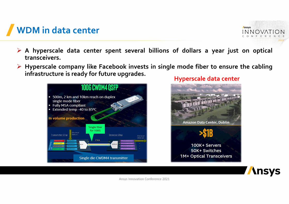
WDM in data center
A hyperscale data center spent several billions of dollars a year just on opticaltransceivers.
Hyperscale company like Facebook invests in single mode fiber to ensure the cablinginfrastructure is ready for future upgrades.
Hyperscale data center

Conventional optical multiplexing technologies
PLC based WDM (de)multiplexers suffer from high optical transmission loss while theassembly of thin-film based WDM (de)multiplexers requires high precisionaxial/angular positioning.
On-chip WDM (de)multiplexing using photonic integration technology is promising.
T. Saeki et al., SEI Technical Review, 2016.

Advantages of photonic integration
Integrating the same photonic functions with easier assembly!

MACOM CDRGe/Si PD
TIA
PLC DeMUX
FiberArray
Optical isolatorSi Lens arraySi
MUXSi MZI modMod Driver
InP/Si Hybrid Laser
Inside Intel’s 100G CWDM4 optical transceiver
InP/Si Hybrid Laser
Si MZI mod 1
Si MZI mod 2
Si MZI mod 3
Si MZI mod 4
RF Pads DC Pads
Echelle grating MUX
Spot size converter

Optical transceiver based on CWDM8
Intel released CWDM8 400 Gbps optical transceivers based on 8-channel CWDM technology.
Wavelength (nm)
12711411 nm
J. B. Driscoll et al., IEEE GFP, 2018.

Roadblock for on-chip WDM (de)multiplexers
(A Blessing and A Curse) Silicon photonics waveguide• Sub-micrometer dimensions• Small bend radius• High-density photonics• Every nm3 matters
Significant filter performance variation across the wafer evenwith advanced CMOS fabrication technology
W. Bogaerts et al., IEEE JSTQE, 2019. (IMEC)

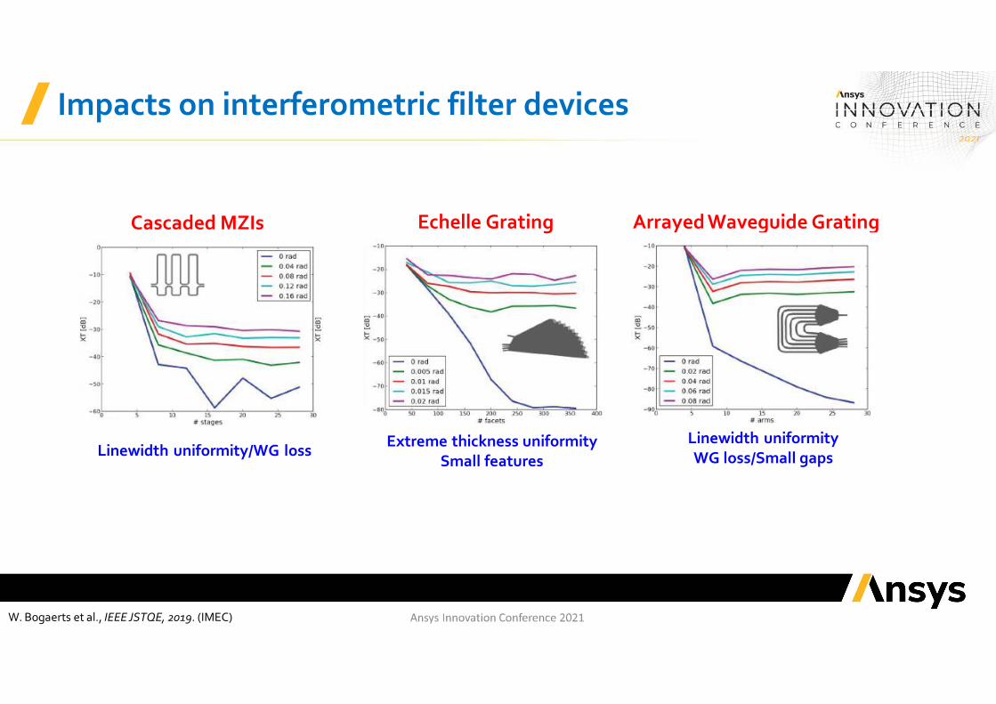
Impacts on interferometric filter devices
W. Bogaerts et al., IEEE JSTQE, 2019. (IMEC)
Cascaded MZIs Arrayed Waveguide GratingEchelle Grating
Linewidth uniformity/WG lossExtreme thickness uniformity
Small featuresLinewidth uniformityWG loss/Small gaps
Impacts on interferometric filter devices
W. Bogaerts et al., IEEE JSTQE, 2019. (IMEC)
Cascaded MZIs Arrayed Waveguide Grating
Linewidth uniformity/WG lossLinewidth uniformityWG loss/Small gaps
Extreme thickness uniformitySmall features
Echelle Grating

Poor device yield in cascaded MZIs
Linewidth variation leads to serious peak wavelength drift of MZIs. Only ~10% device yield !
S.-H. Jeong et al., JOSAB, 2020. (PETRA) W. Bogaerts et al., IEEE JSTQE, 2019. (IMEC)

Outline
Motivations
Fabrication-tolerant MZI design
Cascaded MZIs for WDM (de)multiplexers
Conclusions

The impact of WG dimensional variation
Local (intra-chip) and global (inter-chip) linewidth variation
300-mm SOI wafer demonstrated a thickness variation (3s) of 2.5 nm. Resultant SOI WGsexhibit a linewidth variation (3s) of 7.65 nm.
A wider WG width could effectively reduce the impact of linewidth variation, but this issue cannot be completely eliminated.
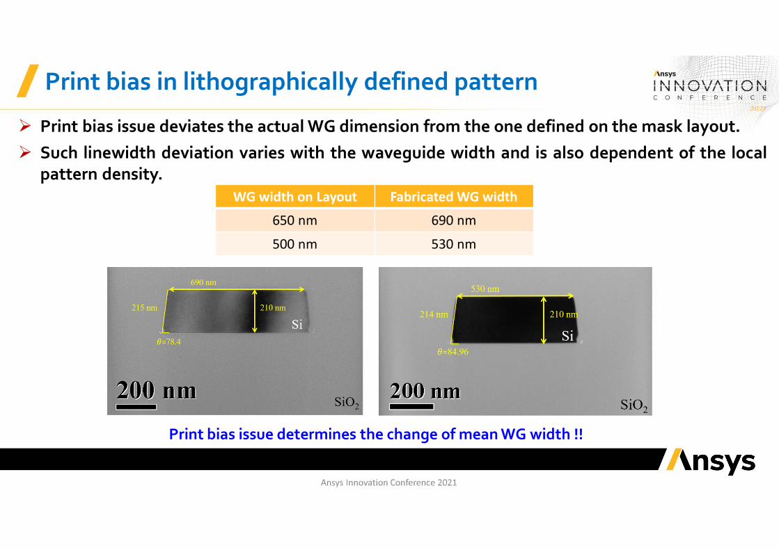
Print bias in lithographically defined pattern
WG width on Layout Fabricated WG width
650 nm 690 nm
500 nm 530 nm
Print bias issue determines the change of mean WG width !!
Print bias issue deviates the actual WG dimension from the one defined on the mask layout. Such linewidth deviation varies with the waveguide width and is also dependent of the local
pattern density.
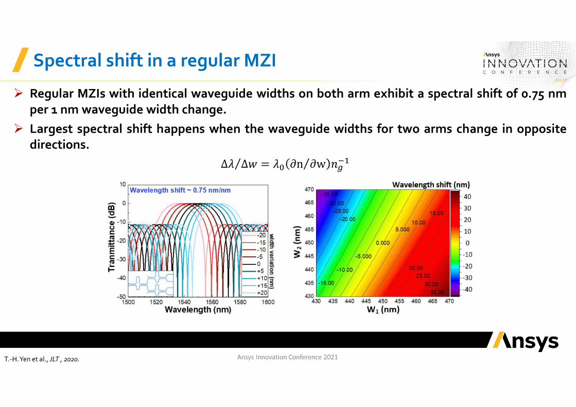
Spectral shift in a regular MZI
Regular MZIs with identical waveguide widths on both arm exhibit a spectral shift of 0.75 nmper 1 nm waveguide width change.
Largest spectral shift happens when the waveguide widths for two arms change in oppositedirections.
∆휆 ∆푤⁄ = 휆 휕n 휕w⁄ 푛
T.-H. Yen et al., JLT , 2020.

The proposed fabrication-tolerant MZI design
This approach allows the cancellation of the effective index change to the waveguide widthvariation in a MZI by combining narrow and wide waveguides on two different arms.
∆휆 ∆푤⁄ = 휆휕푛휕푤 퐿 −
휕푛휕푤 퐿 푛 퐿 − 푛 퐿
Waveguide width dependent spectral shift in a MZI
푛 , = 푛 , − , 휆
∆휆 ∆푤⁄ = 휆 휕n 휕w⁄ 푛
퐿 − 퐿 =0
δλ = 휆 푛 , 퐿 − 푛 , 퐿
Fabrication tolerant MZI design:
T.-H. Yen et al., JLT , 2020.

Spectral shift in a fabrication-tolerant MZI
Spectral shift in a fabrication-tolerant MZI can be relaxed when the waveguide width of twoarms are changed simultaneously with the print bias value.
퐿 − 퐿 =0
δλ = 휆 푛 , 퐿 − 푛 , 퐿
T.-H. Yen et al., JLT , 2020.

Outline
Motivations
Fabrication-tolerant MZI design
Cascaded MZIs for WDM (de)multiplexers
Conclusions

Four-channel CWDM (de)multiplexer – design
T.-H. Yen et al., JLT , 2020.
Four-stage cascaded MZIs 21 fabrication-tolerant MZIs DCs with 5 different coupling ratios Designed for 1510, 1530, 1550, and 1570 nm of wavelengths

Four-channel CWDM (de)multiplexer – experiments
193-nm DUV lithography Edge coupler pair for optical I/Os Footprint: 1.68x0.87 mm (further reduced by smaller bends) W1/W2 = 650/450 nm; L1/L2 = 23.25/8.014 mm
Regular MZIs Fabrication-tolerant MZIs
T.-H. Yen et al., JLT , 2020.

Four-channel CWDM (de)multiplexer – device yield
Regular MZIs
Fabrication-tolerant MZIs
T.-H. Yen et al., JLT , 2020.

Four-channel CWDM (de)multiplexer – performance
T.-H. Yen et al., JLT , 2020.
Precise alignment to the defined wavelength grids leads to lower insertion loss and channelcrosstalk in fabrication-tolerant MZIs.
Degraded channel crosstalk in CH1 is attributed to the narrowband spectral response ofdirectional couplers. The coupling coefficient at CH1 wavelength deviates from the one atdesigned wavelength.

Roadblocks for dense WDM (de)multiplexer
Large device footprint for dense WDM (de)multiplexer Implementing multiple cascaded MZI stages is not practical.
Channel spacing = 4.5 nm
Channel spacing = 0.8 nm
1-1 Regular MZIs
1-1 Compensated MZIs
Channel spacing = 0.08 nm
1-1 Regular MZIs
1-1 Compensated MZIs
1-1 Regular MZIs
1-1 Compensated MZIs
3-2 Regular MZIs
3-2 Compensated MZIs
T.-H. Yen et al., Proc. OECC 2020.

Measured spectral responses (fabrication-tolerant MZIs)
1-1 cascaded MZIs (FSR = 4.5 nm) 1-1 cascaded MZIs (FSR = 0.8 nm) 1-1 cascaded MZIs (FSR = 0.08 nm)
Wavelength (nm)
Opt
ical
tran
smis
sion
(dB)
Wavelength (nm)
Opt
ical
tran
smis
sion
(dB)
Wavelength (nm)
Opt
ical
tran
smis
sion
(dB)
1-1 cascaded MZIs does not provide box-like filter response. No active phase tuning is employed. So process variation induced spectral shift affects the
ultimate optical crosstalk.
T.-H. Yen et al., Proc. OECC 2020.
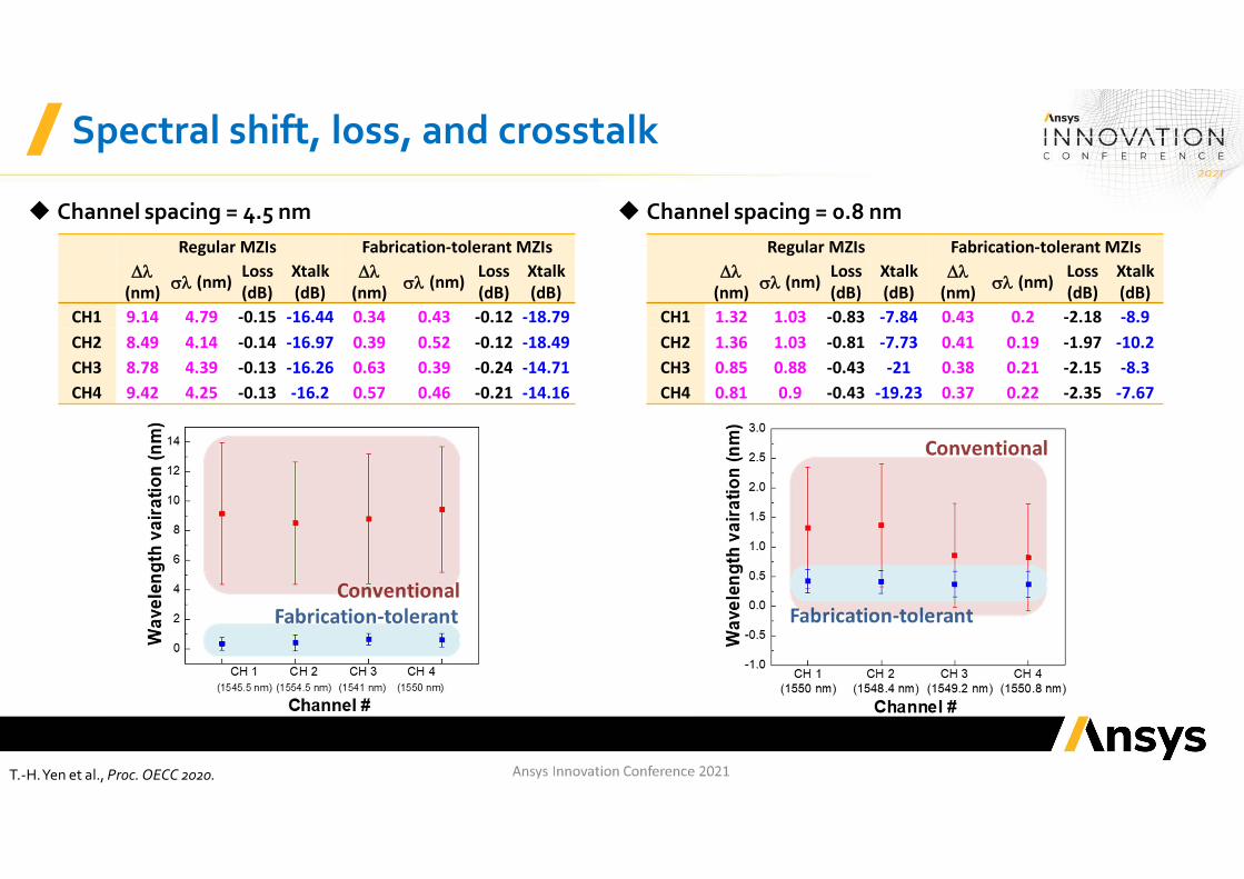
Spectral shift, loss, and crosstalk
T.-H. Yen et al., Proc. OECC 2020.
Regular MZIs Fabrication-tolerant MZIsDl
(nm) sl (nm) Loss (dB)
Xtalk(dB)
Dl(nm) sl (nm) Loss
(dB)Xtalk(dB)
CH1 9.14 4.79 -0.15 -16.44 0.34 0.43 -0.12 -18.79CH2 8.49 4.14 -0.14 -16.97 0.39 0.52 -0.12 -18.49CH3 8.78 4.39 -0.13 -16.26 0.63 0.39 -0.24 -14.71CH4 9.42 4.25 -0.13 -16.2 0.57 0.46 -0.21 -14.16
Regular MZIs Fabrication-tolerant MZIsDl
(nm) sl (nm) Loss (dB)
Xtalk(dB)
Dl(nm) sl (nm) Loss
(dB)Xtalk(dB)
CH1 1.32 1.03 -0.83 -7.84 0.43 0.2 -2.18 -8.9CH2 1.36 1.03 -0.81 -7.73 0.41 0.19 -1.97 -10.2CH3 0.85 0.88 -0.43 -21 0.38 0.21 -2.15 -8.3CH4 0.81 0.9 -0.43 -19.23 0.37 0.22 -2.35 -7.67
Channel spacing = 4.5 nm Channel spacing = 0.8 nm

Actively-tuned cascaded MZIs for dense WDM
Fabrication-tolerant MZI design can reduce the spectral shift to the order of sub-nm. This approach is promising for coarse WDM applications. However, for dense WDM (de)multiplexing we still need active phase tuning to precisely align
each MZI for optimal optical crosstalk.
FSR = 0.083 nm
10.5 dB
1549.7 1549.8 1549.9 1550.0 1550.1 1550.2 1550.3-45
-40
-35
-30
-25
-20
-15
-10
-5
0 1549.921549.96 1550.04
1550
Opt
ical
tran
smis
sion
(dB)
Wavelength (nm)
Ch. 1 (1V) Ch. 3 (2.1V) Ch. 2 (1V) Ch. 3 (2.1V)
FSR = 0.038 nm
11.1 dB
1549.8 1550.0 1550.2-45
-40
-35
-30
-25
-20
-15
-10
-5
0T = 25.3℃
1549.841549.92 1550.08
1550O
ptic
al tr
ansm
issi
on (d
B)
Ch. 1 (1.05V) Ch. 2 (1.05V) Ch. 3 (1.78V) Ch. 4 (1.78V)
1549.7 1549.8 1549.9 1550.0 1550.1 1550.2 1550.3-45
Wavelength (nm)
Outline
Motivations
Fabrication-tolerant MZI design
Cascaded MZIs for WDM (de)multiplexers
Conclusions

Conclusions
T.-H. Yen et al., Proc. OECC 2020.
Due to the manufacturing linewidth variability, serious spectral drift happens in as-fabricated MZIs on silicon-on-insulator.
A fabrication-tolerant MZI design methodology is demonstrated to solve this issue byoptimizing the waveguide widths/lengths of two arms.
Four-channel CWDM (de)multiplexer based on fabrication-tolerant cascaded MZIsexhibit lower insertion loss (< -3dB) and channel crosstalk (< -20 dB) with its spectralresponses well aligned to the defined wavelength grids.
The same design concept can be applied for dense WDM, but cascaded MZIs exhibithigher channel crosstalk and larger device footprint.
Actively optical phase tuning may be required for dense WDM (de)multiplexing.

Acknowledgements
Funding agencies:
Fabrication support:
Software supports:

Thank you for your attention!