Embed Size (px)
Citation preview
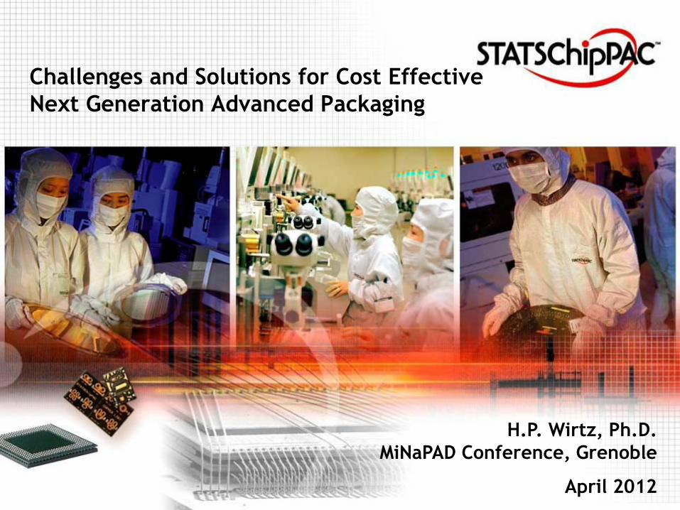
H.P. Wirtz, Ph.D.
MiNaPAD Conference, Grenoble
April 2012
Challenges and Solutions for Cost Effective
Next Generation Advanced Packaging
Confidential
2 2
Outline
•Next Generation Package Requirements
•eWLB (Fan-Out Wafer Level package)
– Introduction to eWLB
– Innovations in eWLB platform
– eWLB Status at STATS ChipPAC
• fcCuBE
•Summary
Confidential
3 3
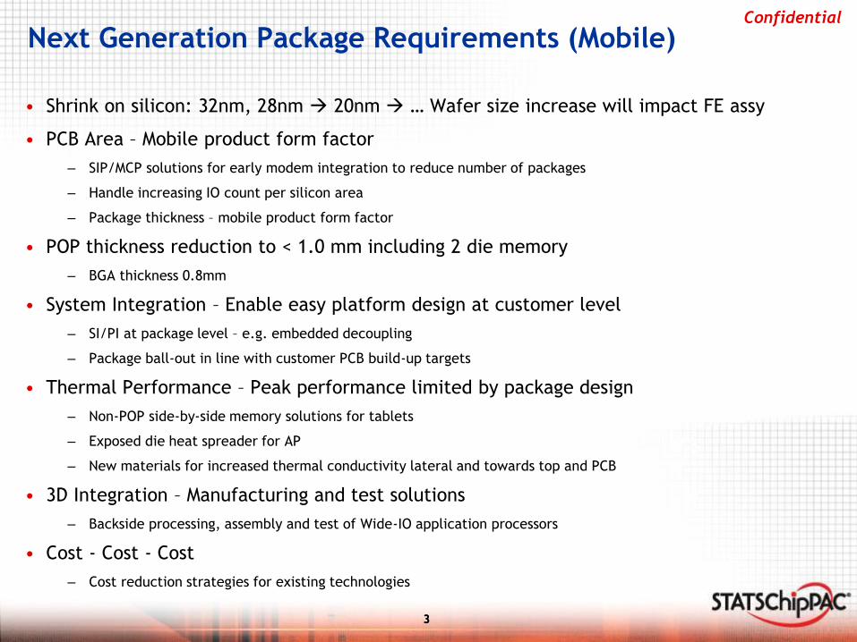
Next Generation Package Requirements (Mobile)
• Shrink on silicon: 32nm, 28nm 20nm … Wafer size increase will impact FE assy
• PCB Area – Mobile product form factor
– SIP/MCP solutions for early modem integration to reduce number of packages
– Handle increasing IO count per silicon area
– Package thickness – mobile product form factor
• POP thickness reduction to < 1.0 mm including 2 die memory
– BGA thickness 0.8mm
• System Integration – Enable easy platform design at customer level
– SI/PI at package level – e.g. embedded decoupling
– Package ball-out in line with customer PCB build-up targets
• Thermal Performance – Peak performance limited by package design
– Non-POP side-by-side memory solutions for tablets
– Exposed die heat spreader for AP
– New materials for increased thermal conductivity lateral and towards top and PCB
• 3D Integration – Manufacturing and test solutions
– Backside processing, assembly and test of Wide-IO application processors
• Cost - Cost - Cost
– Cost reduction strategies for existing technologies
Confidential
4 4
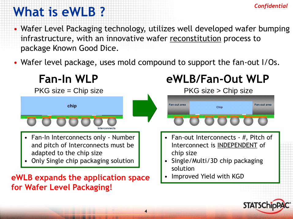
What is eWLB ? • Wafer Level Packaging technology, utilizes well developed wafer bumping
infrastructure, with an innovative wafer reconstitution process to
package Known Good Dice.
• Wafer level package, uses mold compound to support the fan-out I/Os.
• Fan-In Interconnects only - Number
and pitch of Interconnects must be
adapted to the chip size
• Only Single chip packaging solution
• Fan-out Interconnects - #, Pitch of
Interconnect is INDEPENDENT of
chip size
• Single/Multi/3D chip packaging
solution
• Improved Yield with KGD
Fan-In WLP eWLB/Fan-Out WLP PKG size = Chip size PKG size > Chip size
chip
eWLB expands the application space
for Wafer Level Packaging!
Confidential
5 5
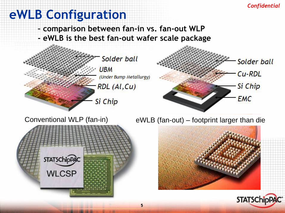
eWLB Configuration
– comparison between fan-in vs. fan-out WLP
- eWLB is the best fan-out wafer scale package
Conventional WLP (fan-in) eWLB (fan-out) – footprint larger than die
Confidential
6 6
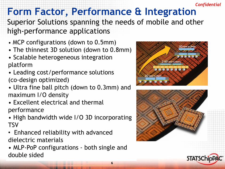
Form Factor, Performance & Integration Superior Solutions spanning the needs of mobile and other
high-performance applications
• MCP configurations (down to 0.5mm)
• The thinnest 3D solution (down to 0.8mm)
• Scalable heterogeneous integration
platform
• Leading cost/performance solutions
(co-design optimized)
• Ultra fine ball pitch (down to 0.3mm) and
maximum I/O density
• Excellent electrical and thermal
performance
• High bandwidth wide I/O 3D incorporating
TSV
• Enhanced reliability with advanced
dielectric materials
• MLP-PoP configurations - both single and
double sided
Confidential
7 7
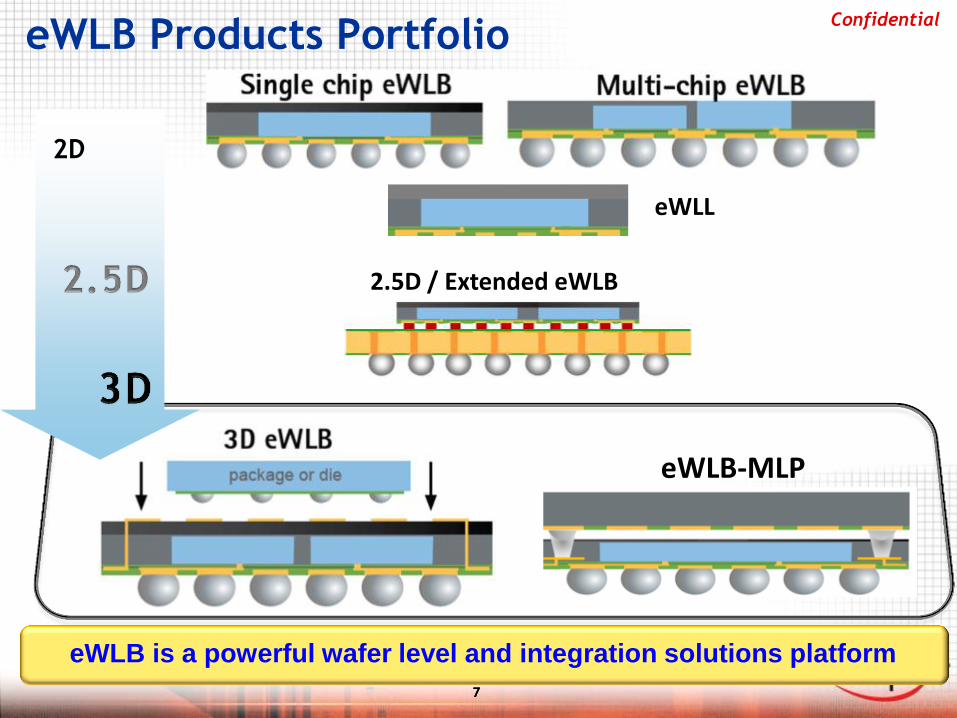
eWLB Products Portfolio
eWLB-MLP
2.5D / Extended eWLB
2D
eWLL
eWLB is a powerful wafer level and integration solutions platform
Confidential
8 8
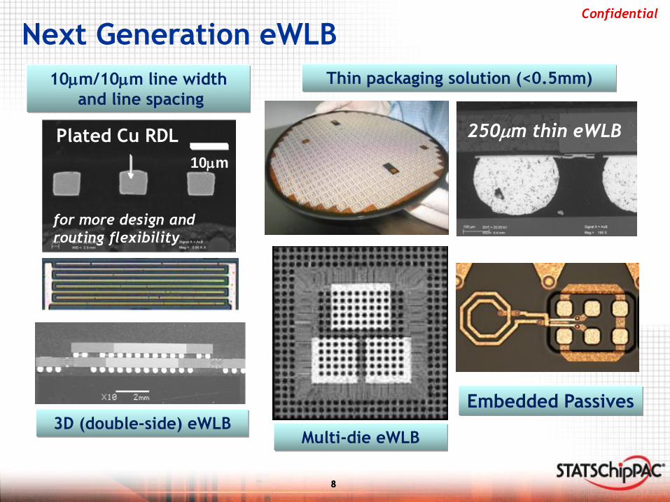
Thin packaging solution (<0.5mm)
Embedded Passives
Multi-die eWLB
Plated Cu RDL
10mm
for more design and
routing flexibility
10mm/10mm line width
and line spacing
3D (double-side) eWLB
250mm thin eWLB
Next Generation eWLB
Confidential
9 9
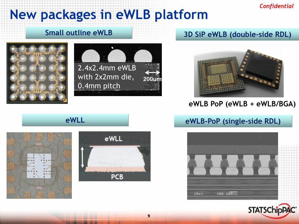
Small outline eWLB
New packages in eWLB platform
200um
eWLL
2.4x2.4mm eWLB
with 2x2mm die,
0.4mm pitch
3D SiP eWLB (double-side RDL)
eWLB PoP (eWLB + eWLB/BGA)
eWLB-PoP (single-side RDL)
Confidential
10 10
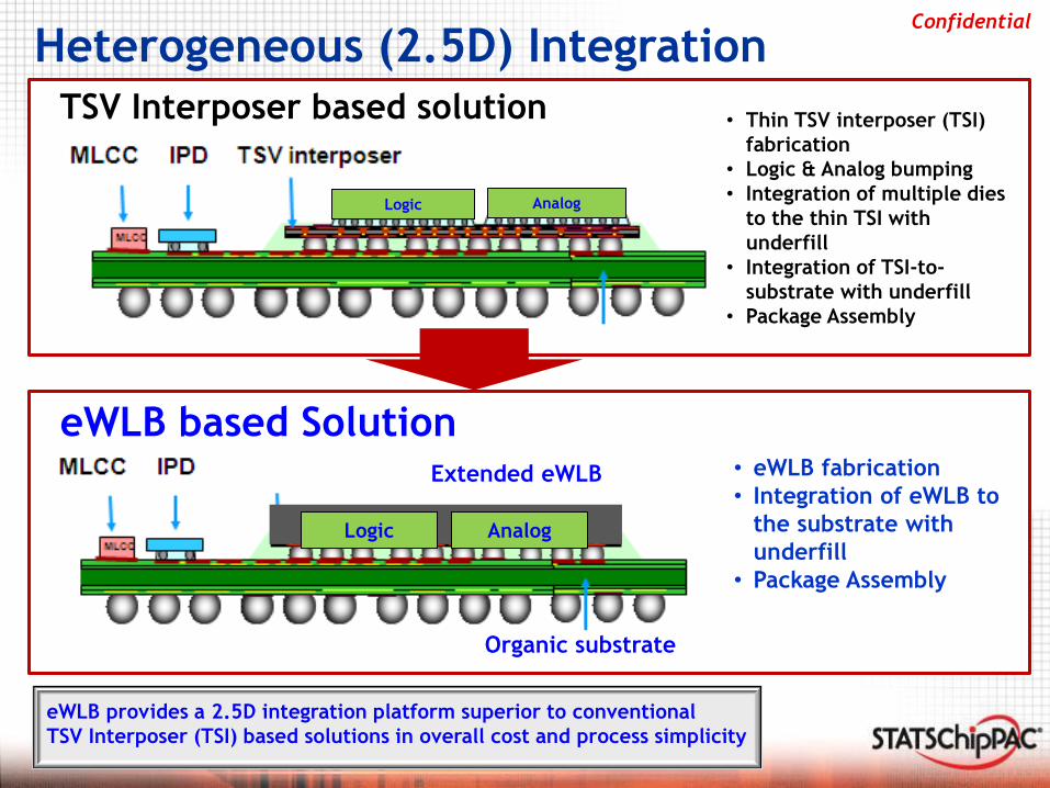
Heterogeneous (2.5D) Integration
Logic Analog
TSV Interposer based solution • Thin TSV interposer (TSI)
fabrication
• Logic & Analog bumping
• Integration of multiple dies
to the thin TSI with
underfill
• Integration of TSI-to-
substrate with underfill
• Package Assembly
eWLB provides a 2.5D integration platform superior to conventional
TSV Interposer (TSI) based solutions in overall cost and process simplicity
Extended eWLB
Logic Analog
eWLB based Solution • eWLB fabrication
• Integration of eWLB to
the substrate with
underfill
• Package Assembly
Organic substrate
Confidential
11 11
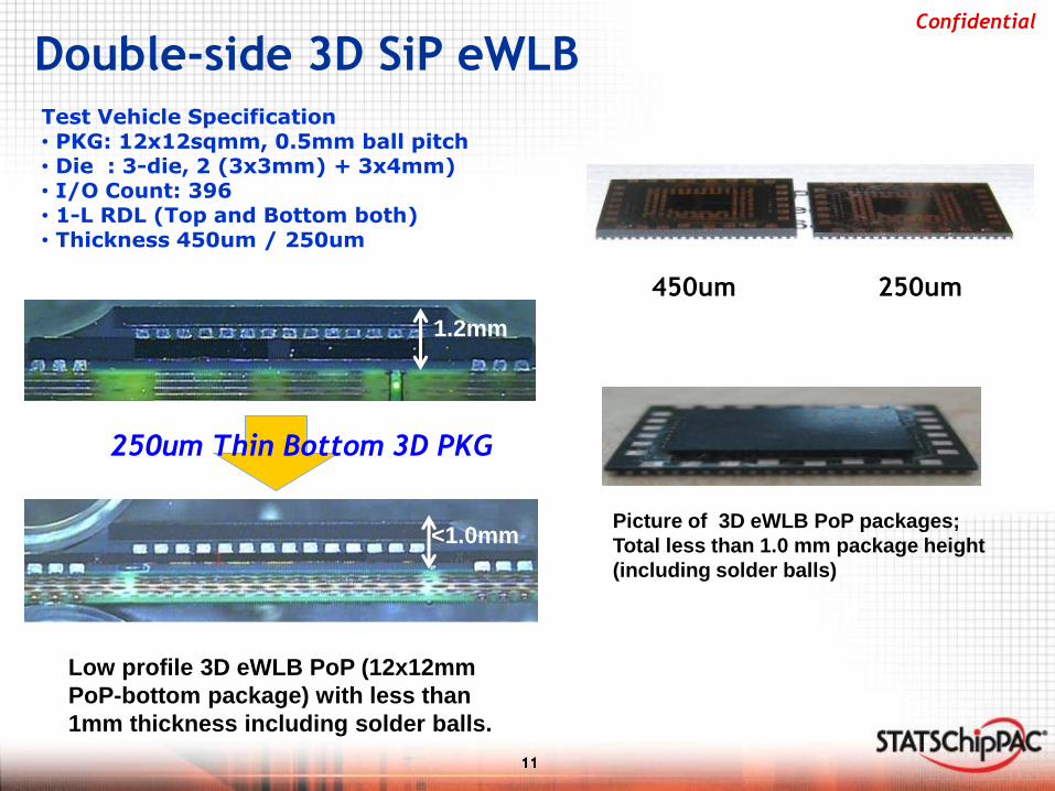
Double-side 3D SiP eWLB Test Vehicle Specification • PKG: 12x12sqmm, 0.5mm ball pitch • Die : 3-die, 2 (3x3mm) + 3x4mm) • I/O Count: 396 • 1-L RDL (Top and Bottom both) • Thickness 450um / 250um
450um 250um
Low profile 3D eWLB PoP (12x12mm
PoP-bottom package) with less than
1mm thickness including solder balls.
1.2mm
<1.0mm
250um Thin Bottom 3D PKG
Picture of 3D eWLB PoP packages;
Total less than 1.0 mm package height
(including solder balls)
Confidential
12 12
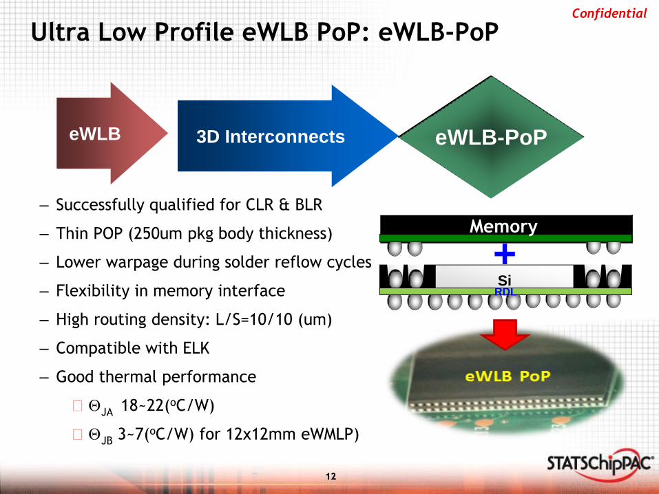
Ultra Low Profile eWLB PoP: eWLB-PoP
– Successfully qualified for CLR & BLR
– Thin POP (250um pkg body thickness)
– Lower warpage during solder reflow cycles
– Flexibility in memory interface
– High routing density: L/S=10/10 (um)
– Compatible with ELK
– Good thermal performance
QJA 18~22(oC/W)
QJB 3~7(oC/W) for 12x12mm eWMLP)
Si RDL
3D Interconnects eWLB
eWLB-PoP
+ Memory
Confidential
13 13
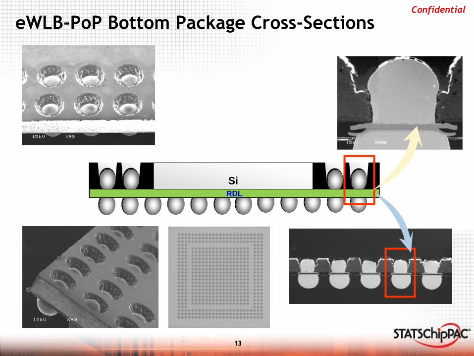
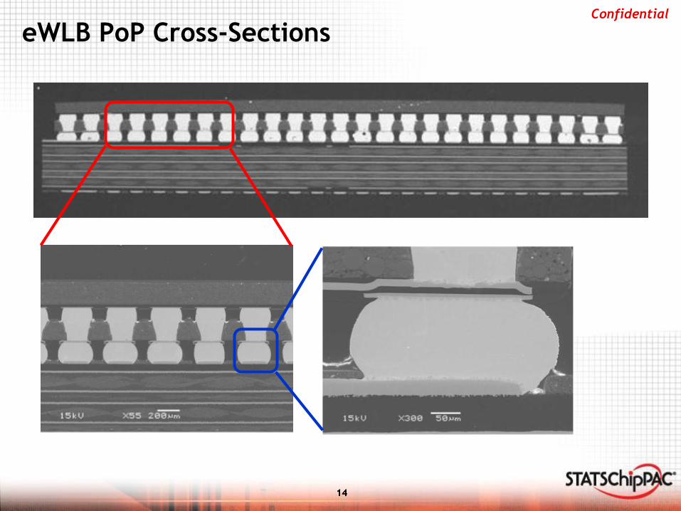
Si RDL
eWLB-PoP Bottom Package Cross-Sections
Confidential
14 14
eWLB PoP Cross-Sections
Confidential
15 15
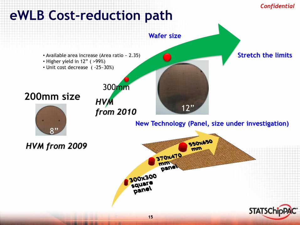
eWLB Cost-reduction path
New Technology (Panel, size under investigation)
300mm
Wafer size
200mm size
8”
HVM from 2009
HVM
from 2010
Stretch the limits • Available area increase (Area ratio ~ 2.35)
• Higher yield in 12” ( >99%)
• Unit cost decrease ( -25~30%)
12”
Confidential
16 16
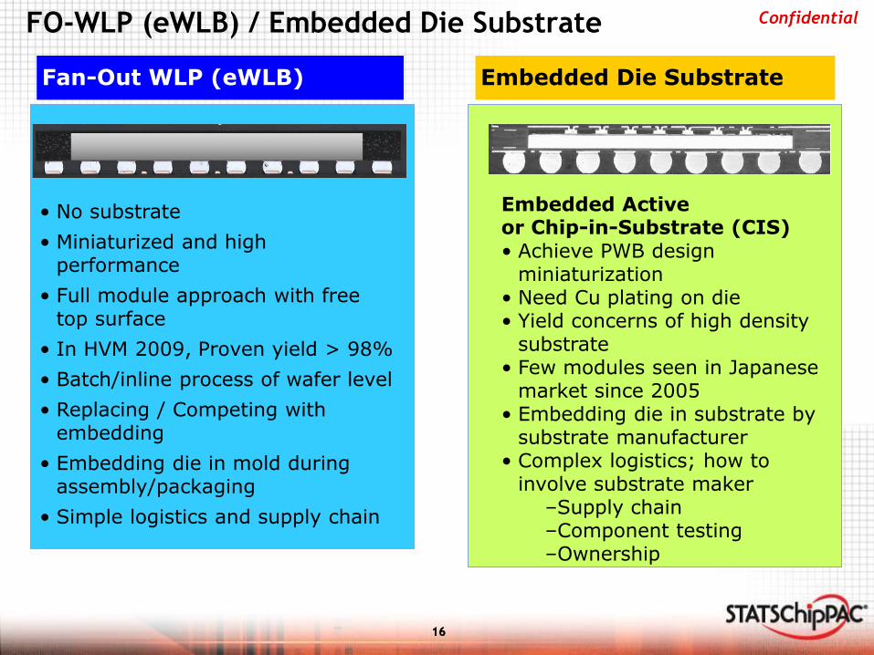
FO-WLP (eWLB) / Embedded Die Substrate
Fan-Out WLP (eWLB) Embedded Die Substrate
• No substrate
• Miniaturized and high performance
• Full module approach with free top surface
• In HVM 2009, Proven yield > 98%
• Batch/inline process of wafer level
• Replacing / Competing with embedding
• Embedding die in mold during assembly/packaging
• Simple logistics and supply chain
Embedded Active or Chip-in-Substrate (CIS)
• Achieve PWB design miniaturization
• Need Cu plating on die • Yield concerns of high density
substrate • Few modules seen in Japanese
market since 2005 • Embedding die in substrate by
substrate manufacturer • Complex logistics; how to
involve substrate maker –Supply chain –Component testing –Ownership
Confidential
17 17
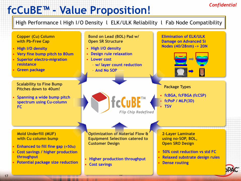
fcCuBE™ - Value Proposition!
2-Layer Laminate
using no-SOP, BOL,
Open SRO Design
Copper (Cu) Column
with Pb-Free Cap
Optimization of Material Flow &
Equipment Selection catered to
Customer Design
TM
Flip Chip Redefined
Scalability to Fine Bump
Pitches down to 40um! Package Types
Bond on Lead (BOL) Pad w/
Open SR Structure
Elimination of ELK/ULK
Damage on Advanced Si
Nodes (40/28nm) -> 20N
High Performance l High I/O Density l ELK/ULK Reliability l Fab Node Compatibility
• High I/O density
• Very fine bump pitch to 80um
• Superior electro-migration
resistance
• Green package
• 50% cost reduction vs std FC
• Relaxed substrate design rules
• Dense routing
• Higher production throughput
• Cost savings
• High I/O density
• Design rule relaxation
• Lower cost
– w/ layer count reduction
– And No SOP
17
• Spanning a wide bump pitch
spectrum using Cu-column
FC
• fcBGA, fcFBGA (fcCSP)
• fcPoP / MLP(3D)
• TSV
• Enhanced to fill fine gap (<50u)
• Cost savings / higher production
throughput
• Potential package size reduction
Mold Underfill (MUF)
with Cu column bump
Confidential
18 18
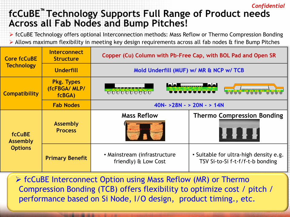
fcCuBE™ Technology Supports Full Range of Product needs Across all Fab Nodes and Bump Pitches!
Core fcCuBE
Technology
Interconnect
Structure Copper (Cu) Column with Pb-Free Cap, with BOL Pad and Open SR
Underfill Mold Underfill (MUF) w/ MR & NCP w/ TCB
Compatibility
Pkg. Types
(fcFBGA/ MLP/
fcBGA)
Fab Nodes 40N- >28N - > 20N - > 14N
fcCuBE
Assembly
Options
Assembly
Process
Mass Reflow (fcCuBE-MF)
Thermo Compression Bonding (fcCuBE-TCB)
Primary Benefit • Mainstream (infrastructure
friendly) & Low Cost
• Suitable for ultra-high density e.g.
TSV Si-to-Si f-t-f/f-t-b bonding
fcCuBE Technology offers optional Interconnection methods: Mass Reflow or Thermo Compression Bonding
Allows maximum flexibility in meeting key design requirements across all fab nodes & fine Bump Pitches
80
fcCuBE Interconnect Option using Mass Reflow (MR) or Thermo
Compression Bonding (TCB) offers flexibility to optimize cost / pitch /
performance based on Si Node, I/O design, product timing., etc.
Confidential
19 19
Summary
• Wafer level packaging is a key technology enabler for future heterogeneous integration with improved electrical performance in the thinnest 3D solution available.
• STATS ChipPAC started 200mm eWLB HVM in 2009.
• Started world’s first 300mm eWLB HVM in 2010 and currently with yield at 99.8%
• Shipped over 600K (8” & 12”) carriers to major mobile OEMs.
• Expanding capacity to meet strong market needs
• eWLB has an aggressive cost reduction path with aggressive annual cost reduction rate from an already competitive cost structure.
• Expand eWLB application area beyond mobile applications 2.5D, 3D, Interposer
• fcCuBE: Powerful, cost-effective Flip Chip solutions platform with design optimizing flexibility
Confidential
20 20
END of Presentation – Thank You!
Heinz-Peter Wirtz, Ph.D. Product & Technology Marketing
Direct: +41 56 535 72 73 Mobile: +41 78 9 111 487