Embed Size (px)
Citation preview
ceg3420 L6 Cost.1 Fa 1998 UCB
CEG3420Computer Design
Lecture 6: Cost and Design Process
ceg3420 L6 Cost.2 Fa 1998 UCB
Administrative Matters
° Review complete
° Read Chapter 4: ALU, Multiply, Divide, FP Mult
° Load balance of discussion sections
ceg3420 L6 Cost.3 Fa 1998 UCB
Year
Perform
ance
0.1
1
10
100
1000
1965 1970 1975 1980 1985 1990 1995 2000
Microprocessors
Minicomputers
Mainframes
Supercomputers
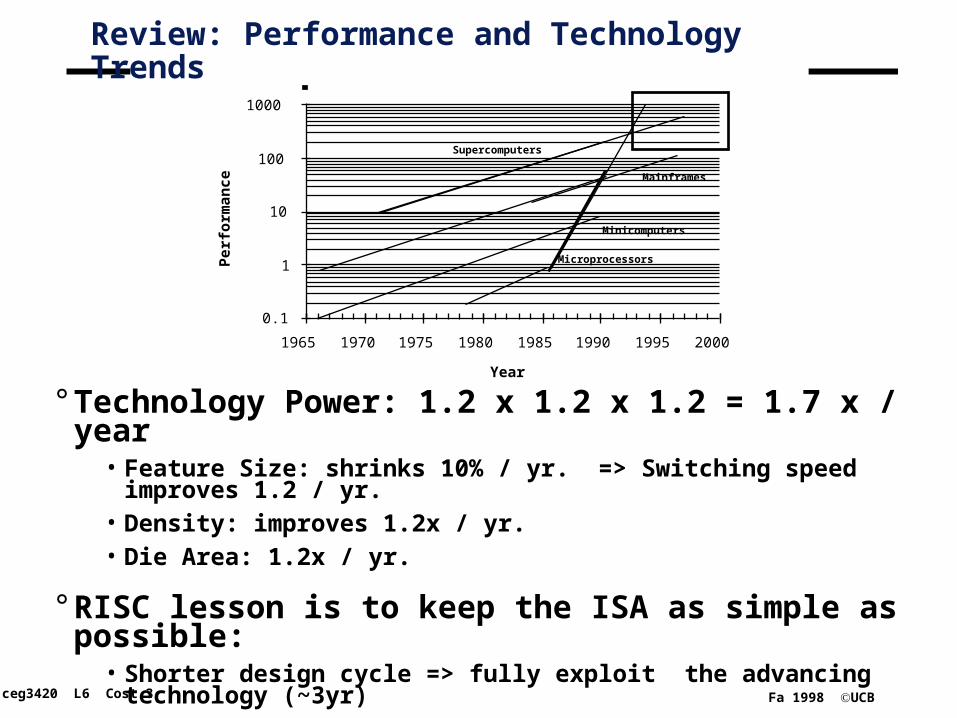
Review: Performance and Technology Trends
° Technology Power: 1.2 x 1.2 x 1.2 = 1.7 x / year• Feature Size: shrinks 10% / yr. => Switching speed improves 1.2 / yr.• Density: improves 1.2x / yr.• Die Area: 1.2x / yr.
° RISC lesson is to keep the ISA as simple as possible:• Shorter design cycle => fully exploit the advancing technology (~3yr)• Advanced branch prediction and pipeline techniques• Bigger and more sophisticated on-chip caches
ceg3420 L6 Cost.4 Fa 1998 UCB
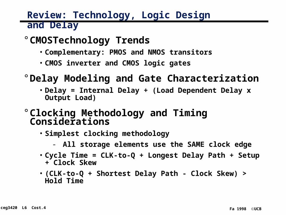
Review: Technology, Logic Design and Delay
° CMOSTechnology Trends• Complementary: PMOS and NMOS transitors
• CMOS inverter and CMOS logic gates
° Delay Modeling and Gate Characterization• Delay = Internal Delay + (Load Dependent Delay x Output Load)
° Clocking Methodology and Timing Considerations• Simplest clocking methodology
- All storage elements use the SAME clock edge
• Cycle Time = CLK-to-Q + Longest Delay Path + Setup + Clock Skew
• (CLK-to-Q + Shortest Delay Path - Clock Skew) > Hold Time
ceg3420 L6 Cost.5 Fa 1998 UCB
Overview: Cost and Design Process
° Cost and Price
° Design process
ceg3420 L6 Cost.6 Fa 1998 UCB
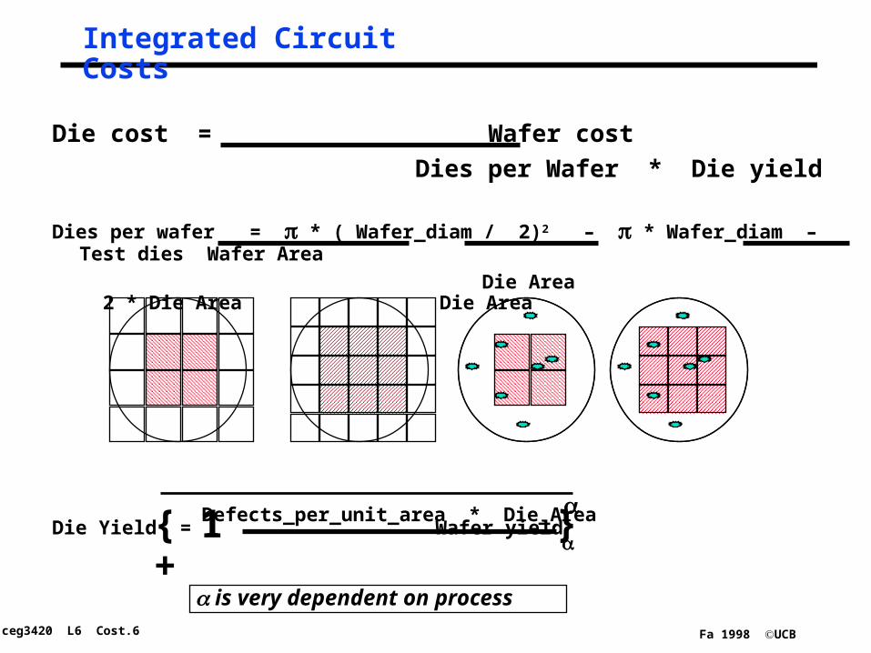
Integrated Circuit Costs
Die cost = Wafer cost
Dies per Wafer * Die yield
Dies per wafer = * ( Wafer_diam / 2)2 – * Wafer_diam – Test dies Wafer Area
Die Area 2 * Die Area Die Area
Die Yield = Wafer yield
is very dependent on process
{ 1+}Defects_per_unit_area * Die_Area
ceg3420 L6 Cost.7 Fa 1998 UCB
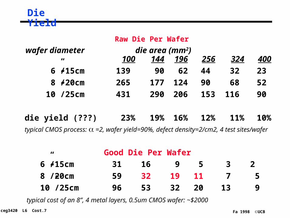
Die Yield
Raw Die Per Wafer
wafer diameter die area (mm2)100 144 196 256 324 400
6”/15cm 139 90 62 44 32 23
8”/20cm 265 177 124 90 68 52
10”/25cm 431 290 206 153 116 90
die yield (???) 23% 19% 16% 12% 11% 10%typical CMOS process: =2, wafer yield=90%, defect density=2/cm2, 4 test sites/wafer
Good Die Per Wafer
6”/15cm 31 16 9 5 3 2
8”/20cm 59 32 19 11 7 5
10”/25cm 96 53 32 20 13 9
typical cost of an 8”, 4 metal layers, 0.5um CMOS wafer: ~$2000
ceg3420 L6 Cost.8 Fa 1998 UCB
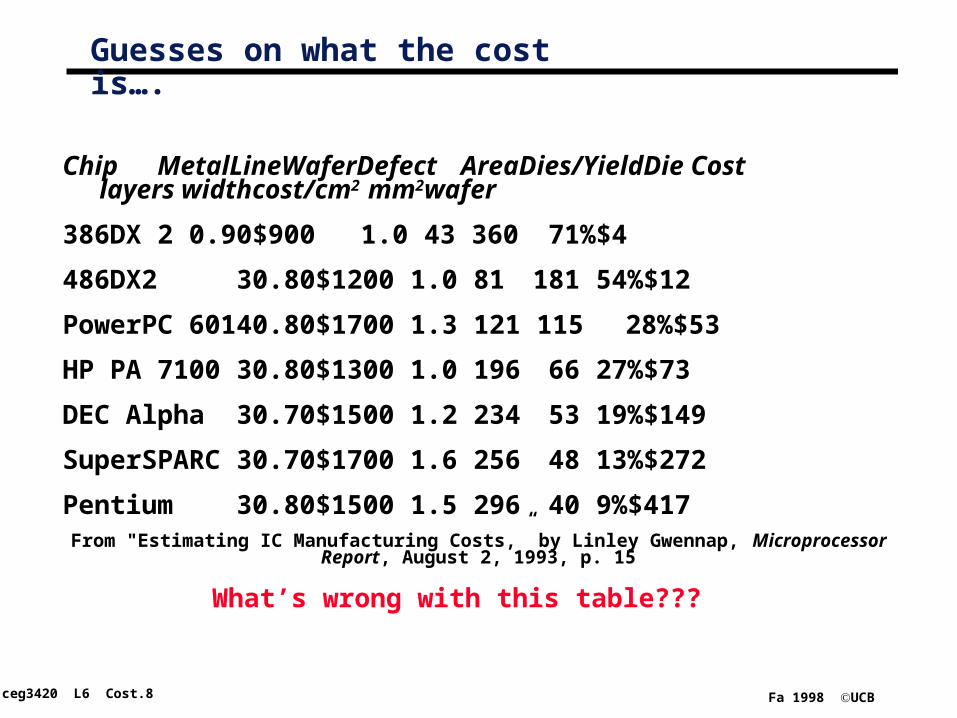
Guesses on what the cost is….
Chip Metal Line Wafer Defect Area Dies/ Yield Die Costlayers width cost /cm2 mm2 wafer
386DX 2 0.90 $900 1.0 43 360 71% $4
486DX2 3 0.80 $1200 1.0 81 181 54% $12
PowerPC 601 4 0.80 $1700 1.3 121 115 28% $53
HP PA 7100 3 0.80 $1300 1.0 196 66 27% $73
DEC Alpha 3 0.70 $1500 1.2 234 53 19% $149
SuperSPARC 3 0.70 $1700 1.6 256 48 13% $272
Pentium 3 0.80 $1500 1.5 296 40 9% $417 From "Estimating IC Manufacturing Costs,” by Linley Gwennap, Microprocessor Report,
August 2, 1993, p. 15
What’s wrong with this table???
ceg3420 L6 Cost.9 Fa 1998 UCB
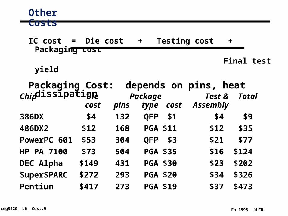
IC cost = Die cost + Testing cost + Packaging cost
Final test yield
Packaging Cost: depends on pins, heat dissipation
Other Costs
Chip Die Package Test & Totalcost pins type cost Assembly
386DX $4 132 QFP $1 $4 $9
486DX2 $12 168 PGA $11 $12 $35
PowerPC 601 $53 304 QFP $3 $21 $77
HP PA 7100 $73 504 PGA $35 $16 $124
DEC Alpha $149 431 PGA $30 $23 $202
SuperSPARC $272 293 PGA $20 $34 $326
Pentium $417 273 PGA $19 $37 $473
ceg3420 L6 Cost.10 Fa 1998 UCB
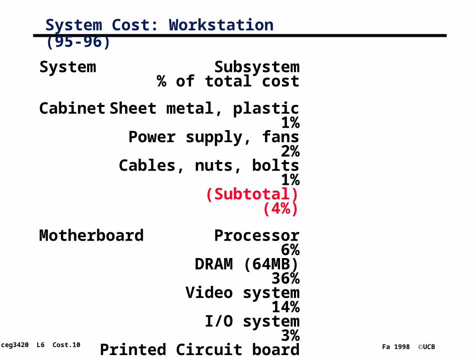
System Cost: Workstation (95-96)
System Subsystem% of total cost
Cabinet Sheet metal, plastic1%
Power supply, fans2%
Cables, nuts, bolts1%
(Subtotal)(4%)
Motherboard Processor6%
DRAM (64MB)36%
Video system14%
I/O system3%
Printed Circuit board1%
(Subtotal)(60%)
I/O Devices Keyboard, mouse1%
Monitor22%
Hard disk (1 GB)7%
Tape drive (DAT)6%
(Subtotal)(36%)
ceg3420 L6 Cost.11 Fa 1998 UCB
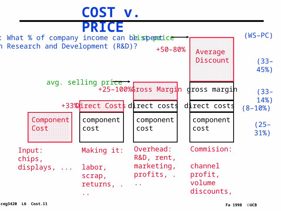
COST v. PRICE
ComponentCost
componentcost
Direct Costs
componentcost
direct costs
Gross Margin
componentcost
direct costs
gross margin
AverageDiscount
list price
avg. selling price
Input: chips, displays, ...
Making it: labor, scrap, returns, ...
Overhead: R&D, rent, marketing, profits, ...
Commision: channel profit, volume discounts,
+33%
+25–100%
+50–80%
(25–31%)
(33–45%)
(8–10%)
(33–14%)
(WS–PC)Q: What % of company income can be spenton Research and Development (R&D)?
ceg3420 L6 Cost.12 Fa 1998 UCB
Cost Summary
° Integrated circuits driving computer industry
° Die cost a strong function of die area
° Economics ($$$) is the ultimate driver for performance!
ceg3420 L6 Cost.13 Fa 1998 UCB
The Design Process
"To Design Is To Represent"
Design activity yields description/representation of an object
-- Traditional craftsman does not distinguish between the conceptualization and the artifact
-- Separation comes about because of complexity
-- The concept is captured in one or more representation languages
-- This process IS design
Design Begins With Requirements
-- Functional Capabilities: what it will do
-- Performance Characteristics: Speed, Power, Area, Cost, . . .
ceg3420 L6 Cost.14 Fa 1998 UCB
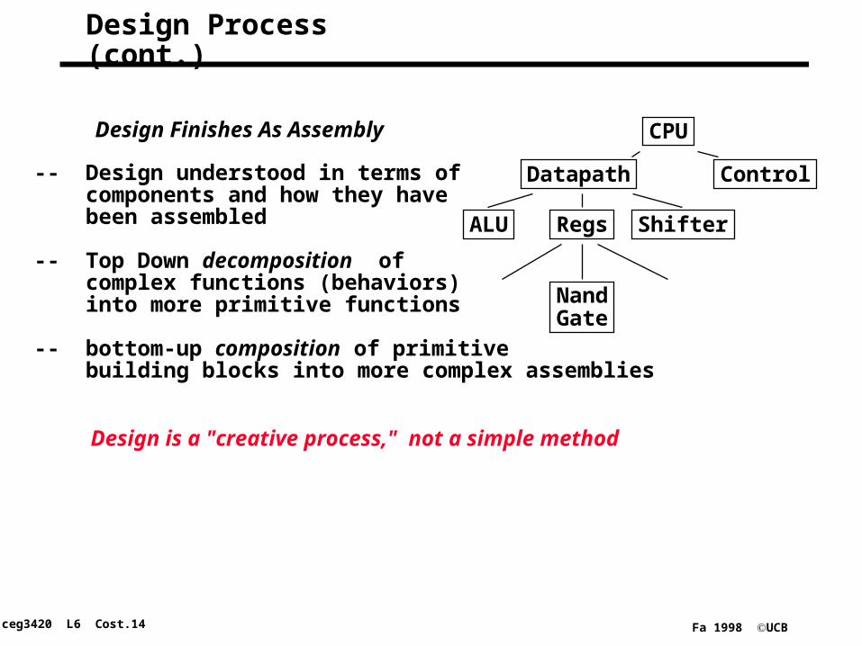
Design Process (cont.)
Design Finishes As Assembly
-- Design understood in terms of components and how they have been assembled
-- Top Down decomposition of complex functions (behaviors) into more primitive functions
-- bottom-up composition of primitive building blocks into more complex assemblies
CPU
Datapath Control
ALU Regs Shifter
NandGate
Design is a "creative process," not a simple method
ceg3420 L6 Cost.15 Fa 1998 UCB
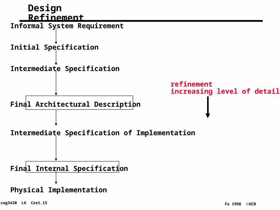
Design Refinement
Informal System Requirement
Initial Specification
Intermediate Specification
Final Architectural Description
Intermediate Specification of Implementation
Final Internal Specification
Physical Implementation
refinementincreasing level of detail
ceg3420 L6 Cost.16 Fa 1998 UCB
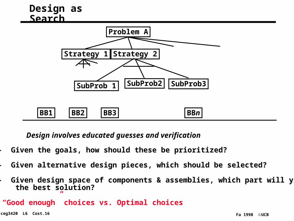
Design as Search
Design involves educated guesses and verification
-- Given the goals, how should these be prioritized?
-- Given alternative design pieces, which should be selected?
-- Given design space of components & assemblies, which part will yield the best solution?
“Good enough” choices vs. Optimal choices
Problem A
Strategy 1 Strategy 2
SubProb 1 SubProb2 SubProb3
BB1 BB2 BB3 BBn
ceg3420 L6 Cost.17 Fa 1998 UCB
Problem: Design a “fast” ALU for the MIPS ISA
° Requirements?
° Must support the Arithmetic / Logic operations
° Tradeoffs of cost and speed based on frequency of occurrence, hardware budget
ceg3420 L6 Cost.18 Fa 1998 UCB
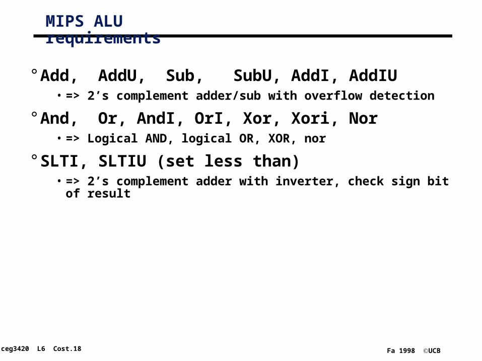
MIPS ALU requirements
° Add, AddU, Sub, SubU, AddI, AddIU • => 2’s complement adder/sub with overflow detection
° And, Or, AndI, OrI, Xor, Xori, Nor• => Logical AND, logical OR, XOR, nor
° SLTI, SLTIU (set less than)• => 2’s complement adder with inverter, check sign bit of result
ceg3420 L6 Cost.19 Fa 1998 UCB
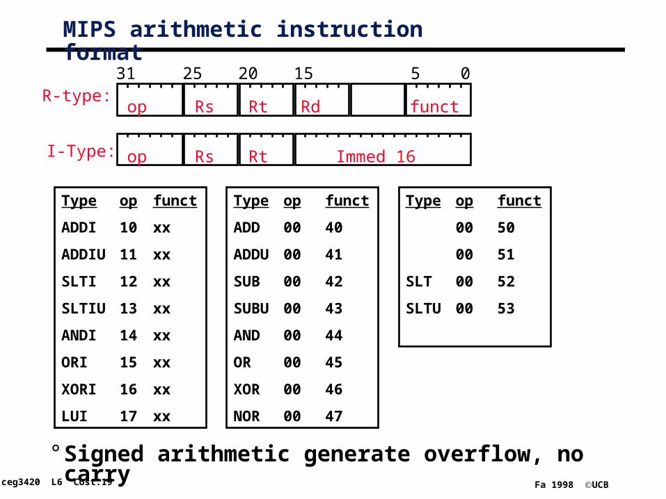
MIPS arithmetic instruction format
° Signed arithmetic generate overflow, no carry
R-type:
I-Type:
31 25 20 15 5 0
op Rs Rt Rd funct
op Rs Rt Immed 16
Type op funct
ADDI 10 xx
ADDIU 11 xx
SLTI 12 xx
SLTIU 13 xx
ANDI 14 xx
ORI 15 xx
XORI 16 xx
LUI 17 xx
Type op funct
ADD 00 40
ADDU 00 41
SUB 00 42
SUBU 00 43
AND 00 44
OR 00 45
XOR 00 46
NOR 00 47
Type op funct
00 50
00 51
SLT 00 52
SLTU 00 53
ceg3420 L6 Cost.20 Fa 1998 UCB
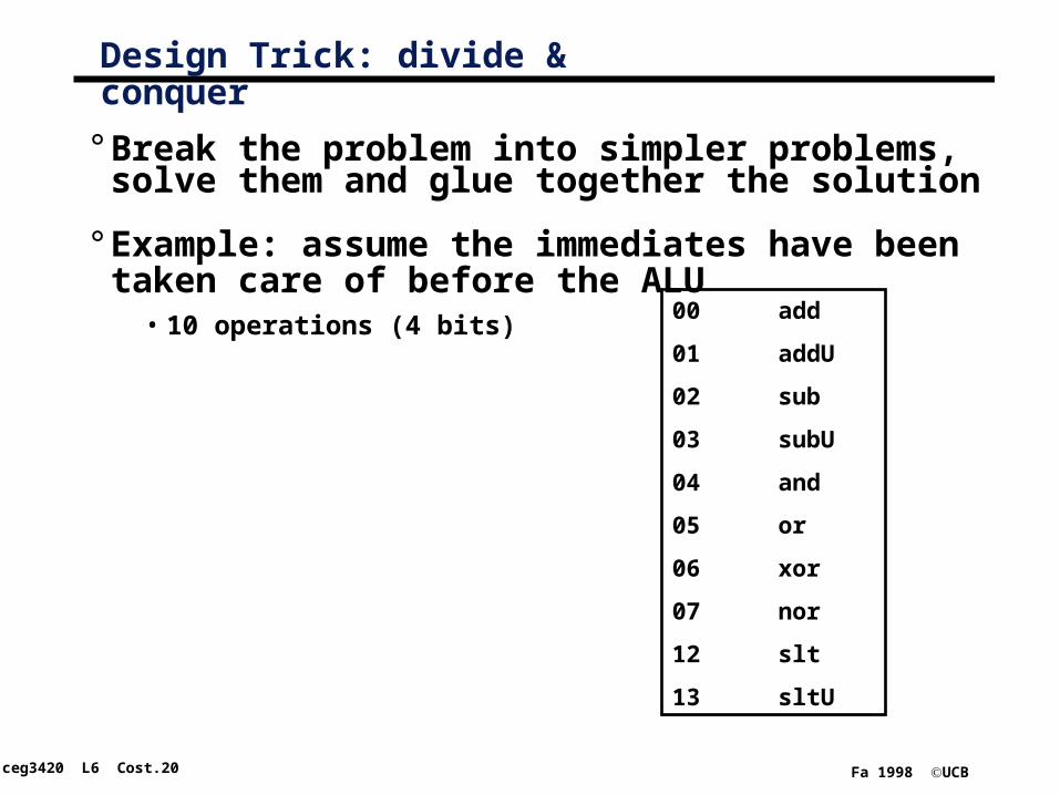
Design Trick: divide & conquer
° Break the problem into simpler problems, solve them and glue together the solution
° Example: assume the immediates have been taken care of before the ALU
• 10 operations (4 bits)00 add
01 addU
02 sub
03 subU
04 and
05 or
06 xor
07 nor
12 slt
13 sltU
ceg3420 L6 Cost.21 Fa 1998 UCB
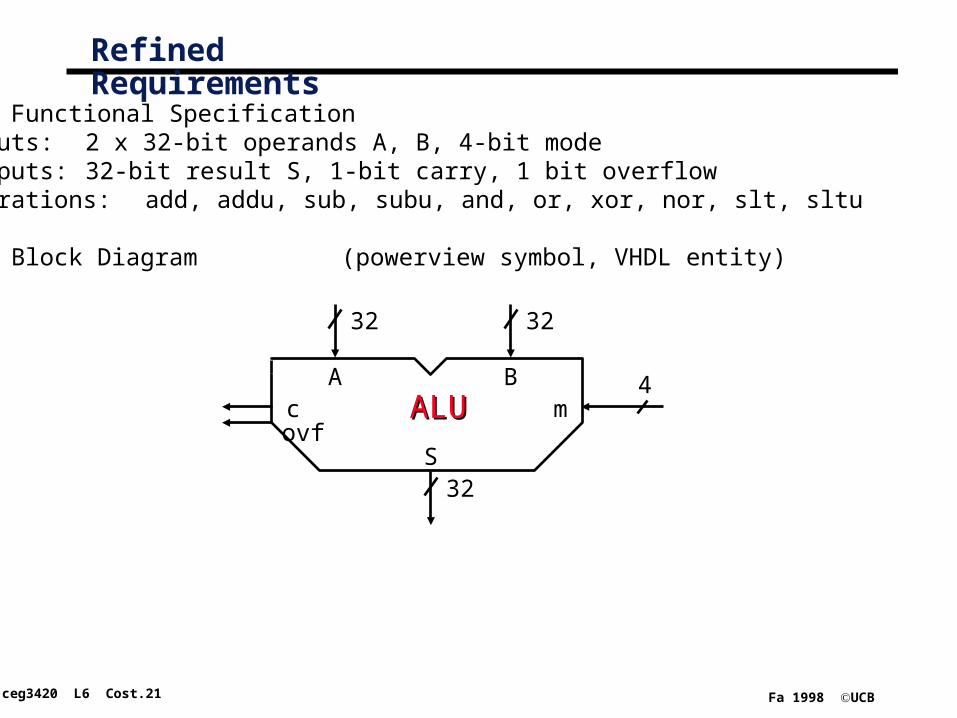
Refined Requirements
(1) Functional Specificationinputs: 2 x 32-bit operands A, B, 4-bit modeoutputs: 32-bit result S, 1-bit carry, 1 bit overflowoperations: add, addu, sub, subu, and, or, xor, nor, slt, sltu
(2) Block Diagram (powerview symbol, VHDL entity)
ALUALUA B
movf
S
32 32
32
4c
ceg3420 L6 Cost.22 Fa 1998 UCB
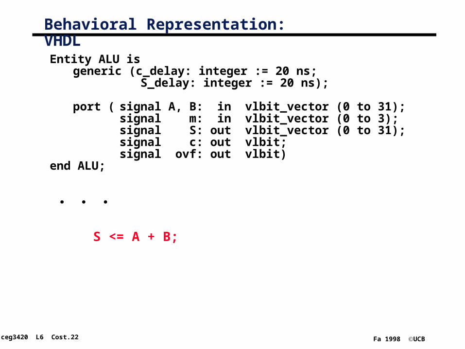
Behavioral Representation: VHDL
Entity ALU isgeneric (c_delay: integer := 20 ns;
S_delay: integer := 20 ns);
port ( signal A, B: in vlbit_vector (0 to 31);signal m: in vlbit_vector (0 to 3);signal S: out vlbit_vector (0 to 31);signal c: out vlbit;signal ovf: out vlbit)
end ALU;
. . .
S <= A + B;

ceg3420 L6 Cost.23 Fa 1998 UCB
Design Decisions
° Simple bit-slice• big combinational problem
• many little combinational problems
• partition into 2-step problem
° Bit slice with carry look-ahead
° . . .
ALU
bit slice
7-to-2 C/L 7 3-to-2 C/L
PLD Gates muxCL0 CL6
ceg3420 L6 Cost.24 Fa 1998 UCB
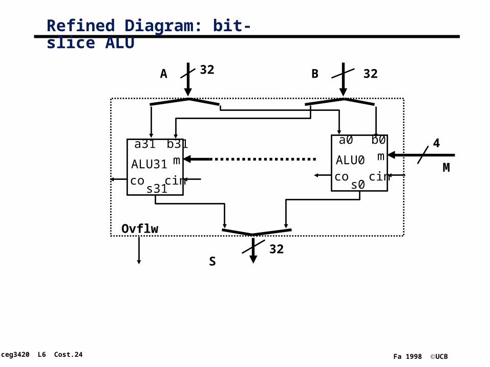
Refined Diagram: bit-slice ALU
A B
M
S
32 32
32
4
Ovflw
ALU0
a0 b0m
cincos0
ALU31
a31 b31m
cincos31
ceg3420 L6 Cost.25 Fa 1998 UCB
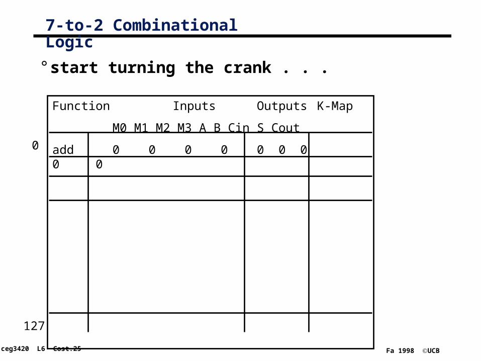
7-to-2 Combinational Logic
° start turning the crank . . .
Function Inputs Outputs K-Map
M0 M1 M2 M3 A B Cin S Cout
add 0 0 0 0 0 0 0 0 00
127
ceg3420 L6 Cost.26 Fa 1998 UCB
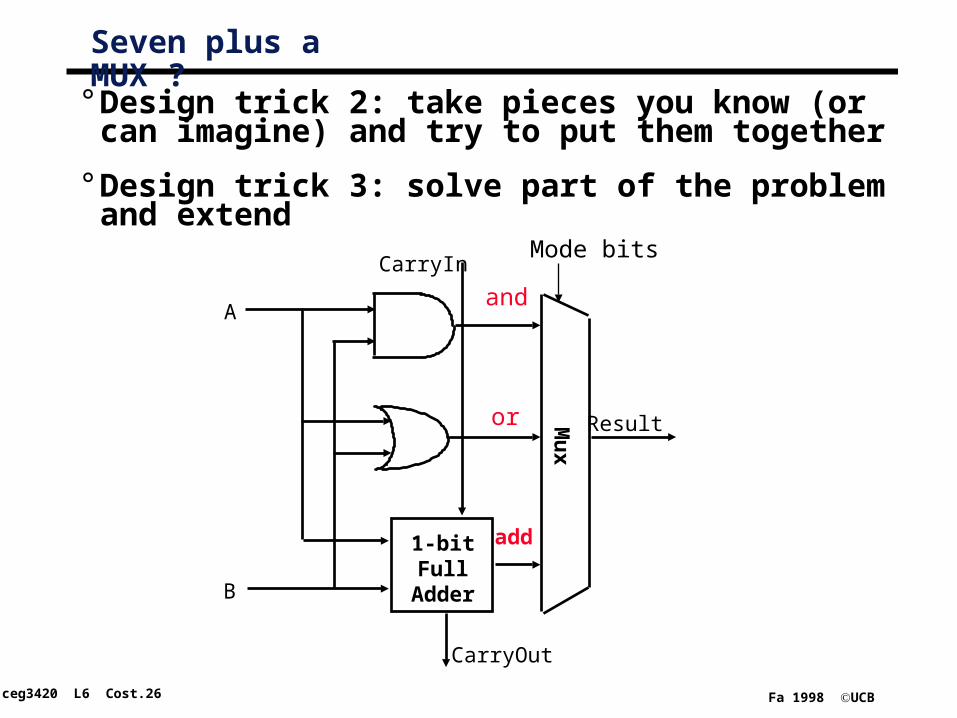
Seven plus a MUX ?
A
B
1-bitFull
Adder
CarryOut
Mu
x
CarryIn
Result
° Design trick 2: take pieces you know (or can imagine) and try to put them together
° Design trick 3: solve part of the problem and extend
add
and
or
Mode bits

ceg3420 L6 Cost.27 Fa 1998 UCB
Additional operations
° A - B = A + (– B)• form two complement by invert and add one
A
B
1-bitFull
Adder
CarryOut
Mu
x
CarryIn
Result
add
and
or
Mode bitsinvert
ceg3420 L6 Cost.28 Fa 1998 UCB
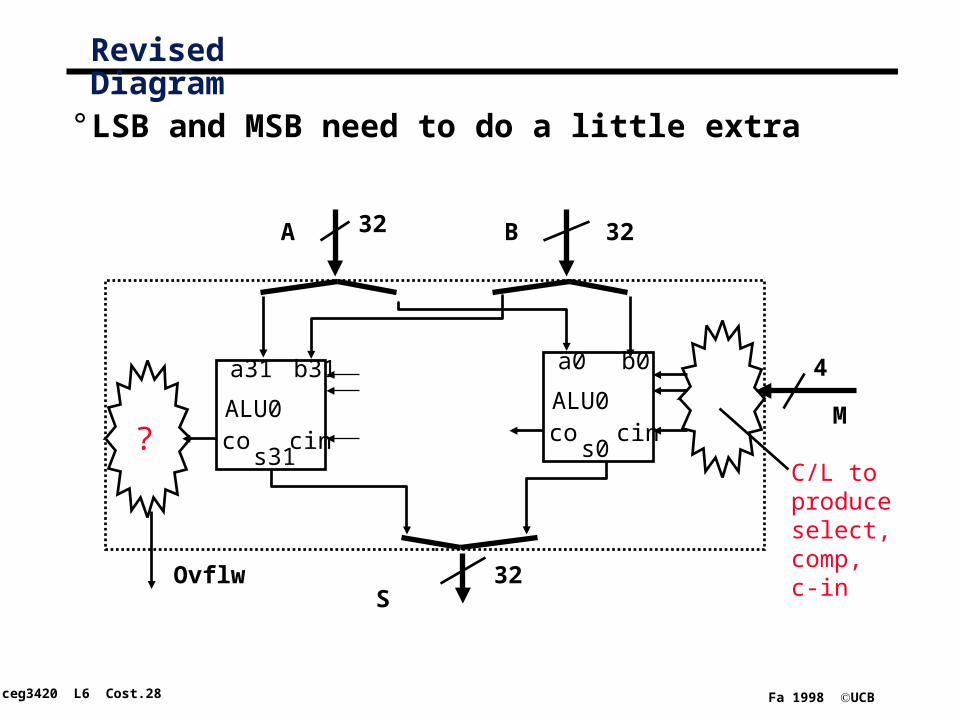
Revised Diagram
° LSB and MSB need to do a little extra
A B
M
S
32 32
32
4
Ovflw
ALU0
a0 b0
cincos0
ALU0
a31 b31
cincos31
C/L toproduceselect,comp,c-in
?
ceg3420 L6 Cost.29 Fa 1998 UCB
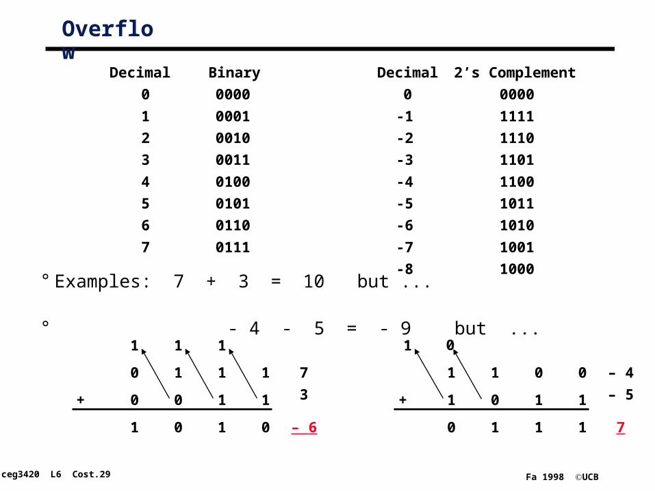
Overflow
° Examples: 7 + 3 = 10 but ...
° - 4 - 5 = - 9 but ...
2’s ComplementBinaryDecimal
0 0000
1 0001
2 0010
3 0011
0000
1111
1110
1101
Decimal
0
-1
-2
-3
4 0100
5 0101
6 0110
7 0111
1100
1011
1010
1001
-4
-5
-6
-7
1000-8
0 1 1 1
0 0 1 1+
1 0 1 0
1
1 1 0 0
1 0 1 1+
0 1 1 1
11 0
7
3
1
– 6
– 4
– 5
7
ceg3420 L6 Cost.30 Fa 1998 UCB
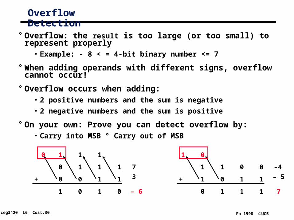
Overflow Detection
° Overflow: the result is too large (or too small) to represent properly
• Example: - 8 < = 4-bit binary number <= 7
° When adding operands with different signs, overflow cannot occur!
° Overflow occurs when adding:• 2 positive numbers and the sum is negative
• 2 negative numbers and the sum is positive
° On your own: Prove you can detect overflow by:• Carry into MSB ° Carry out of MSB
0 1 1 1
0 0 1 1+
1 0 1 0
1
1 1 0 0
1 0 1 1+
0 1 1 1
110
7
3
1
– 6
–4
– 5
7
0
ceg3420 L6 Cost.31 Fa 1998 UCB
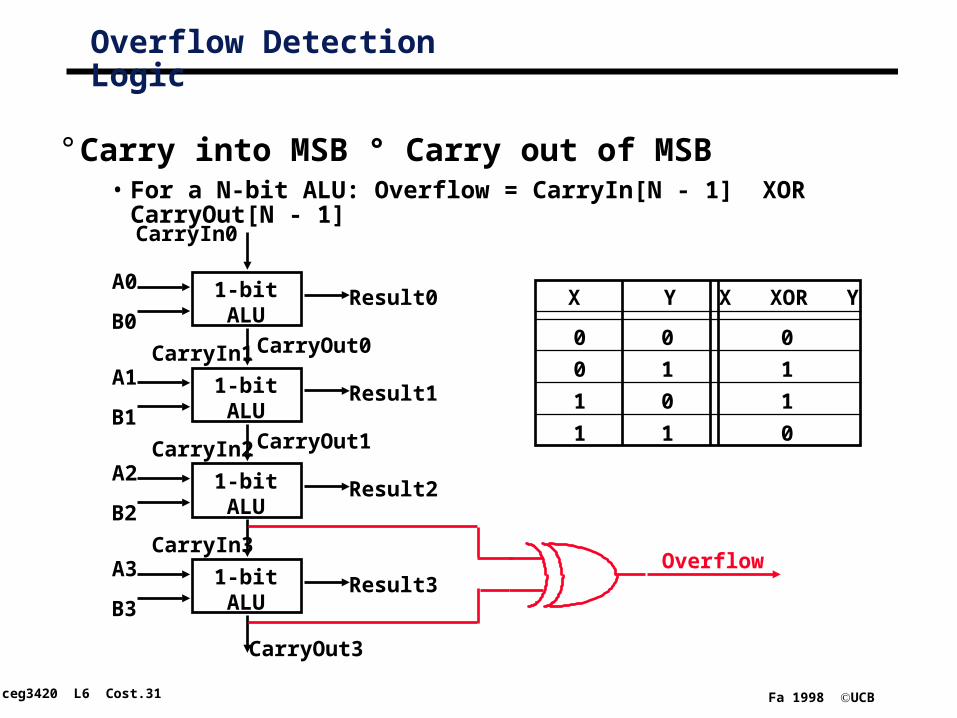
Overflow Detection Logic
° Carry into MSB ° Carry out of MSB• For a N-bit ALU: Overflow = CarryIn[N - 1] XOR CarryOut[N - 1]
A0
B0
1-bitALU
Result0
CarryIn0
CarryOut0
A1
B1
1-bitALU
Result1
CarryIn1
CarryOut1
A2
B2
1-bitALU
Result2
CarryIn2
A3
B3
1-bitALU
Result3
CarryIn3
CarryOut3
Overflow
X Y X XOR Y
0 0 0
0 1 1
1 0 1
1 1 0
ceg3420 L6 Cost.32 Fa 1998 UCB
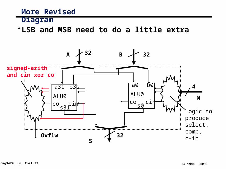
More Revised Diagram
° LSB and MSB need to do a little extra
A B
M
S
32 32
32
4
Ovflw
ALU0
a0 b0
cincos0
ALU0
a31 b31
cincos31
Logic toproduceselect,comp,c-in
signed-arithand cin xor co

ceg3420 L6 Cost.33 Fa 1998 UCB
But What about Performance?
° Critical Path of n-bit Rippled-carry adder is n*CP
A0
B0
1-bitALU
Result0
CarryIn0
CarryOut0
A1
B1
1-bitALU
Result1
CarryIn1
CarryOut1
A2
B2
1-bitALU
Result2
CarryIn2
CarryOut2
A3
B3
1-bitALU
Result3
CarryIn3
CarryOut3
Design Trick: throw hardware at it
ceg3420 L6 Cost.34 Fa 1998 UCB
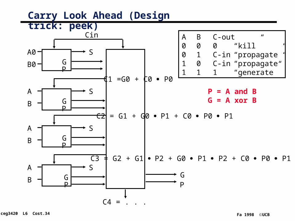
Carry Look Ahead (Design trick: peek)
A B C-out0 0 0 “kill”0 1 C-in “propagate”1 0 C-in “propagate”1 1 1 “generate”
A0
B0
SGP
P = A and BG = A xor B
A
B
SGP
A
B
SGP
A
B
SGP
Cin
C1 =G0 + C0 P0
C2 = G1 + G0 P1 + C0 P0 P1
C3 = G2 + G1 P2 + G0 P1 P2 + C0 P0 P1 P2
G
C4 = . . .
P
ceg3420 L6 Cost.35 Fa 1998 UCB
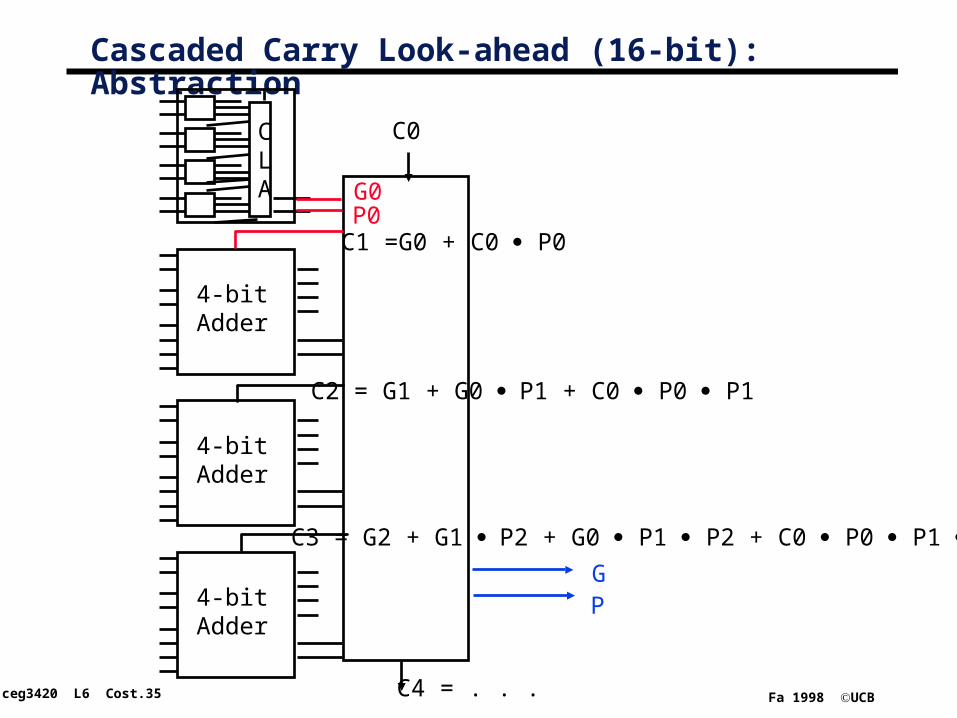
Cascaded Carry Look-ahead (16-bit): Abstraction
CLA
4-bitAdder
4-bitAdder
4-bitAdder
C1 =G0 + C0 P0
C2 = G1 + G0 P1 + C0 P0 P1
C3 = G2 + G1 P2 + G0 P1 P2 + C0 P0 P1 P2
GP
G0P0
C4 = . . .
C0
ceg3420 L6 Cost.36 Fa 1998 UCB
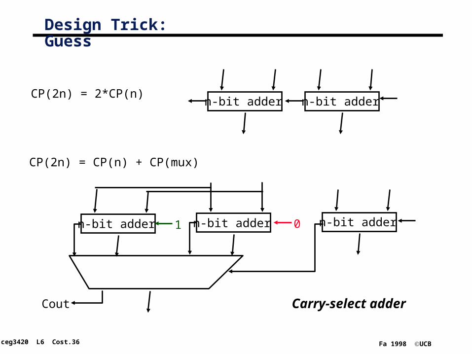
Design Trick: Guess
n-bit adder n-bit adderCP(2n) = 2*CP(n)
n-bit adder n-bit addern-bit adder 1 0
Cout
CP(2n) = CP(n) + CP(mux)
Carry-select adder
ceg3420 L6 Cost.37 Fa 1998 UCB
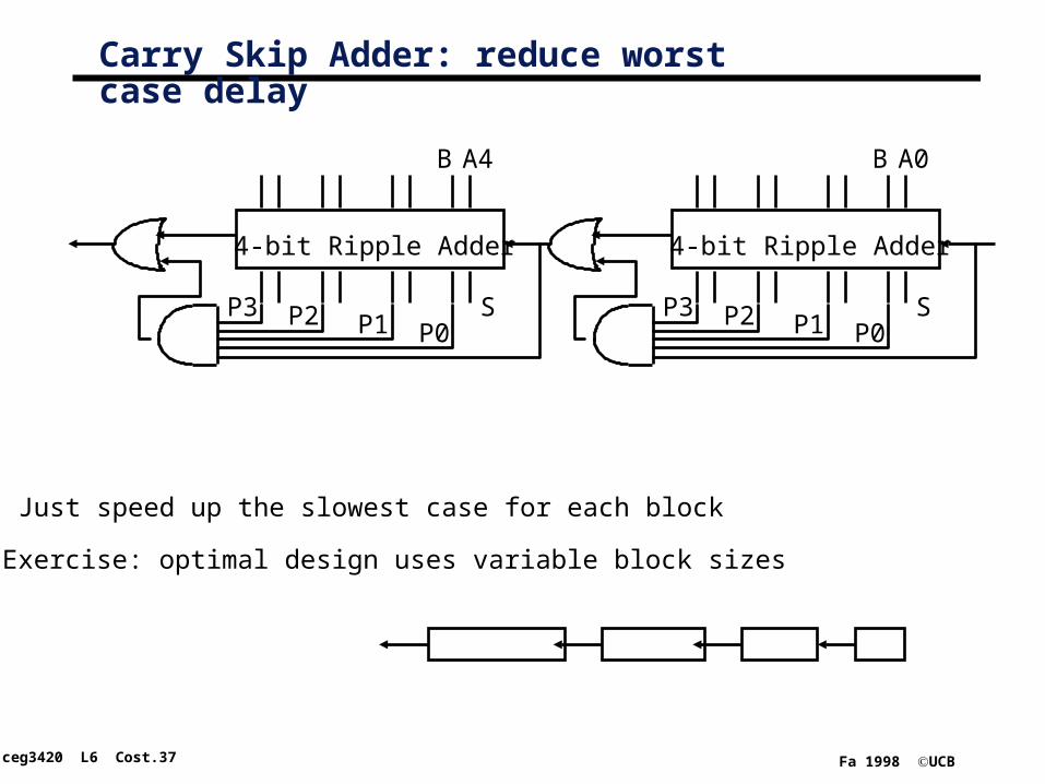
Carry Skip Adder: reduce worst case delay
4-bit Ripple Adder
A0B
SP0P1P2P3
4-bit Ripple Adder
A4B
SP0P1P2P3
Exercise: optimal design uses variable block sizes
Just speed up the slowest case for each block
ceg3420 L6 Cost.38 Fa 1998 UCB
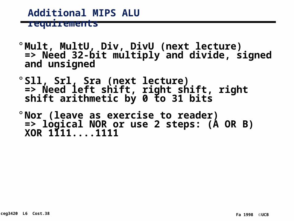
Additional MIPS ALU requirements
° Mult, MultU, Div, DivU (next lecture)=> Need 32-bit multiply and divide, signed and unsigned
° Sll, Srl, Sra (next lecture)=> Need left shift, right shift, right shift arithmetic by 0 to 31 bits
° Nor (leave as exercise to reader)=> logical NOR or use 2 steps: (A OR B) XOR 1111....1111
ceg3420 L6 Cost.39 Fa 1998 UCB
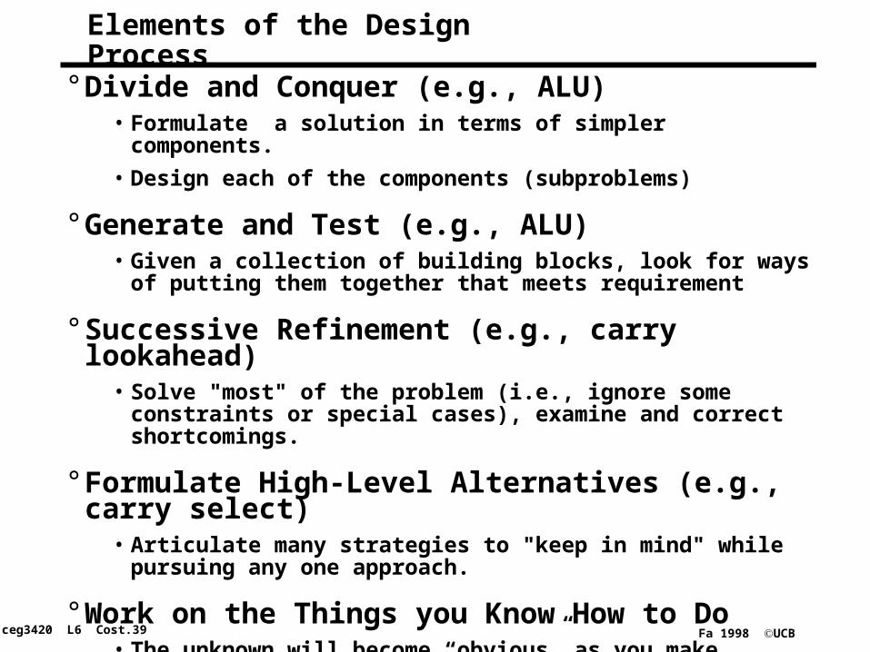
Elements of the Design Process
° Divide and Conquer (e.g., ALU)• Formulate a solution in terms of simpler components.
• Design each of the components (subproblems)
° Generate and Test (e.g., ALU)• Given a collection of building blocks, look for ways of putting
them together that meets requirement
° Successive Refinement (e.g., carry lookahead)• Solve "most" of the problem (i.e., ignore some constraints or
special cases), examine and correct shortcomings.
° Formulate High-Level Alternatives (e.g., carry select)• Articulate many strategies to "keep in mind" while pursuing any
one approach.
° Work on the Things you Know How to Do• The unknown will become “obvious” as you make progress.
ceg3420 L6 Cost.40 Fa 1998 UCB
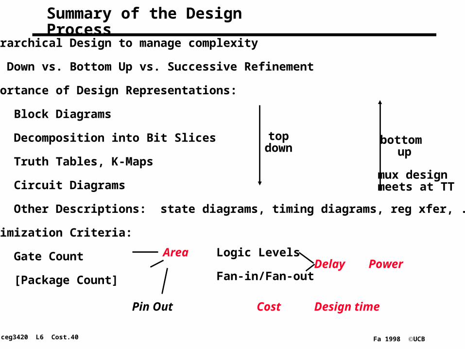
Summary of the Design Process
Hierarchical Design to manage complexity
Top Down vs. Bottom Up vs. Successive Refinement
Importance of Design Representations:
Block Diagrams
Decomposition into Bit Slices
Truth Tables, K-Maps
Circuit Diagrams
Other Descriptions: state diagrams, timing diagrams, reg xfer, . . .
Optimization Criteria:
Gate Count
[Package Count]
Logic Levels
Fan-in/Fan-outPower
topdown
bottom up
AreaDelay
mux designmeets at TT
Cost Design timePin Out
ceg3420 L6 Cost.41 Fa 1998 UCB
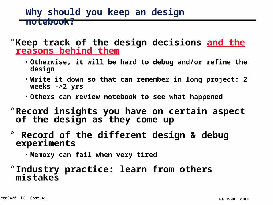
Why should you keep an design notebook?
° Keep track of the design decisions and the reasons behind them
• Otherwise, it will be hard to debug and/or refine the design
• Write it down so that can remember in long project: 2 weeks ->2 yrs
• Others can review notebook to see what happened
° Record insights you have on certain aspect of the design as they come up
° Record of the different design & debug experiments• Memory can fail when very tired
° Industry practice: learn from others mistakes
ceg3420 L6 Cost.42 Fa 1998 UCB
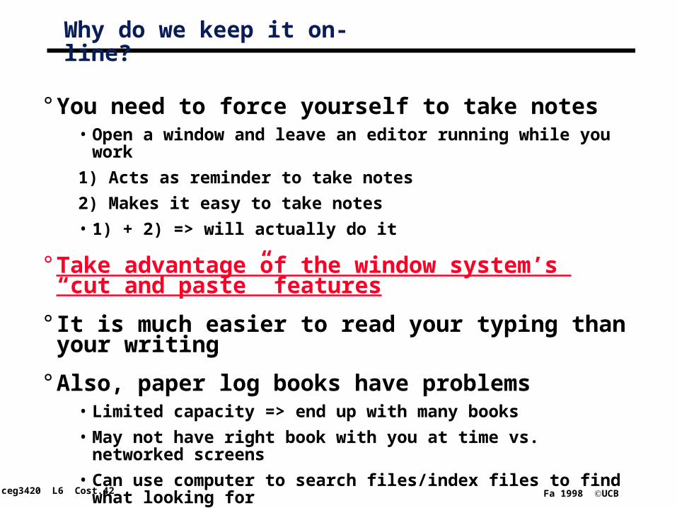
Why do we keep it on-line?
° You need to force yourself to take notes• Open a window and leave an editor running while you work
1) Acts as reminder to take notes
2) Makes it easy to take notes
• 1) + 2) => will actually do it
° Take advantage of the window system’s “cut and paste” features
° It is much easier to read your typing than your writing
° Also, paper log books have problems• Limited capacity => end up with many books
• May not have right book with you at time vs. networked screens
• Can use computer to search files/index files to find what looking for
ceg3420 L6 Cost.43 Fa 1998 UCB
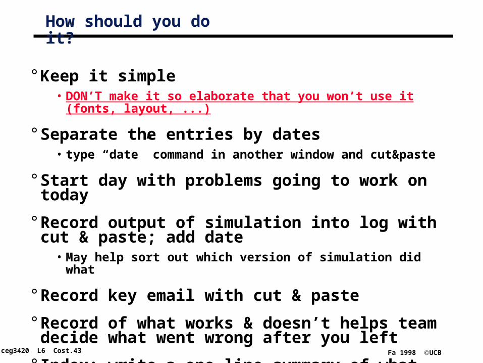
How should you do it?
° Keep it simple• DON’T make it so elaborate that you won’t use it (fonts, layout, ...)
° Separate the entries by dates• type “date” command in another window and cut&paste
° Start day with problems going to work on today
° Record output of simulation into log with cut & paste; add date
• May help sort out which version of simulation did what
° Record key email with cut & paste
° Record of what works & doesn’t helps team decide what went wrong after you left
° Index: write a one-line summary of what you did at end of each day
ceg3420 L6 Cost.44 Fa 1998 UCB
On-line Notebook Example
° Refer to the handout “Example of On-Line Log Book” on cs 152 home page
ceg3420 L6 Cost.45 Fa 1998 UCB
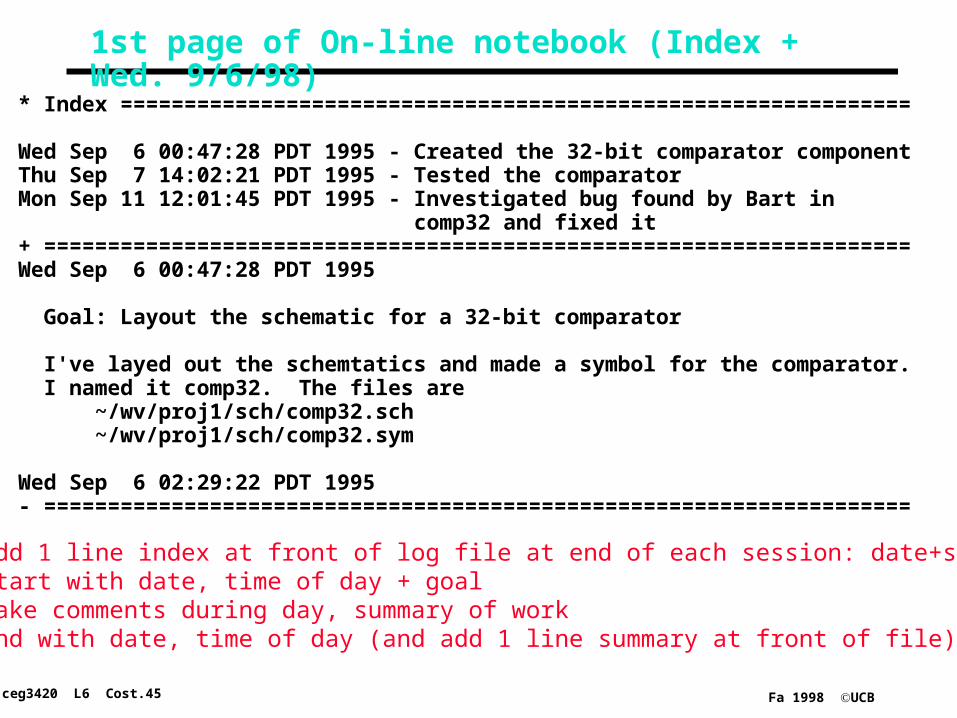
1st page of On-line notebook (Index + Wed. 9/6/98)
* Index ==============================================================
Wed Sep 6 00:47:28 PDT 1995 - Created the 32-bit comparator componentThu Sep 7 14:02:21 PDT 1995 - Tested the comparatorMon Sep 11 12:01:45 PDT 1995 - Investigated bug found by Bart in comp32 and fixed it+ ====================================================================Wed Sep 6 00:47:28 PDT 1995
Goal: Layout the schematic for a 32-bit comparator
I've layed out the schemtatics and made a symbol for the comparator. I named it comp32. The files are ~/wv/proj1/sch/comp32.sch ~/wv/proj1/sch/comp32.sym
Wed Sep 6 02:29:22 PDT 1995- ====================================================================
• Add 1 line index at front of log file at end of each session: date+summary• Start with date, time of day + goal• Make comments during day, summary of work• End with date, time of day (and add 1 line summary at front of file)
ceg3420 L6 Cost.46 Fa 1998 UCB
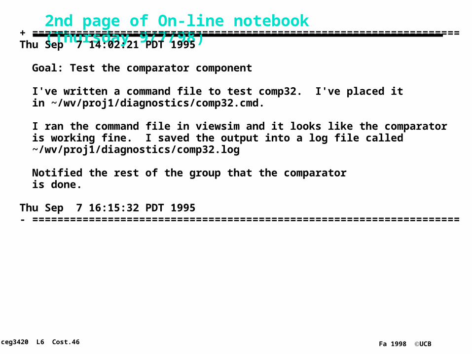
2nd page of On-line notebook (Thursday 9/7/98)+ ====================================================================
Thu Sep 7 14:02:21 PDT 1995
Goal: Test the comparator component
I've written a command file to test comp32. I've placed it in ~/wv/proj1/diagnostics/comp32.cmd.
I ran the command file in viewsim and it looks like the comparator is working fine. I saved the output into a log file called ~/wv/proj1/diagnostics/comp32.log
Notified the rest of the group that the comparator is done.
Thu Sep 7 16:15:32 PDT 1995- ====================================================================
ceg3420 L6 Cost.47 Fa 1998 UCB
3rd page of On-line notebook (Monday 9/11/98)
Mon Sep 11 12:01:45 PDT 1995
Goal: Investigate bug discovered in comp32 and hopefully fix it
Bart found a bug in my comparator component. He left the following e-mail.
-------------------From [email protected] Sun Sep 10 01:47:02 1995Received: by wayne.manor (NX5.67e/NX3.0S) id AA00334; Sun, 10 Sep 95 01:47:01 -0800Date: Wed, 10 Sep 95 01:47:01 -0800From: Bart Simpson <[email protected]>To: [email protected], old_man@gokuraku, hojo@sanctuarySubject: [cs152] bug in comp32Status: R
Hey Bruce,I think there's a bug in your comparator. The comparator seems to think that ffffffff and fffffff7 are equal.
Can you take a look at this?Bart----------------
ceg3420 L6 Cost.48 Fa 1998 UCB
4th page of On-line notebook (9/11/98 contd)
(equal should be 0 instead of 1)------------------SIM>stepsize 10nsSIM>v a_in A[31:0]SIM>v b_in B[31:0]SIM>w a_in b_in equalSIM>a a_in ffffffff\hSIM>a b_in fffffff7\hSIM>simtime = 10.0ns A_IN=FFFFFFFF\H B_IN=FFFFFFF7\H EQUAL=1 Simulation stopped at 10.0ns.-------------------
Ah. I've discovered the bug. I mislabeled the 4th net in the comp32 schematic.
I corrected the mistake and re-checked all the other labels, just in case.
I re-ran the old diagnostic test file and tested it against the bug Bart found. It seems to be working fine. hopefully there aren’t any more bugs:)
ceg3420 L6 Cost.49 Fa 1998 UCB
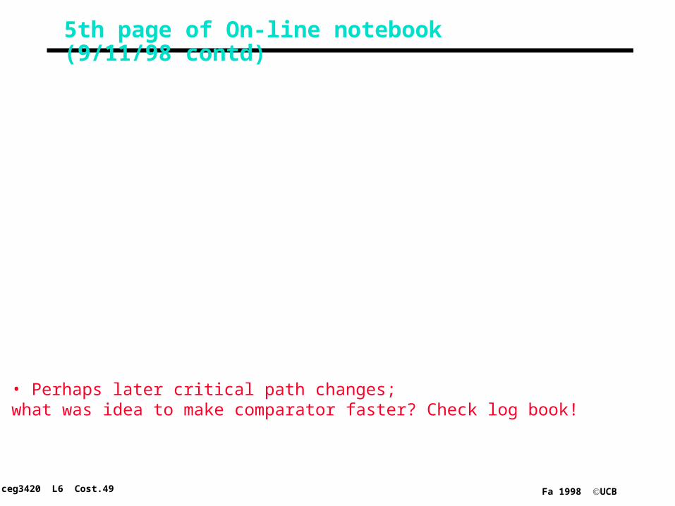
5th page of On-line notebook (9/11/98 contd)
remove one level of gates in the design and make it go faster. But who cares! the comparator is not in the critical path right now. the delay through the ALU is dominating the critical path. so unless the ALU gets a lot faster, we can live with a less than optimal comparator.
I e-mailed the group that the bug has been fixed
Mon Sep 11 14:03:41 PDT 1995- ====================================================================
• Perhaps later critical path changes; what was idea to make comparator faster? Check log book!
ceg3420 L6 Cost.50 Fa 1998 UCB
Lecture Summary
° Cost and Price• Die size determines chip cost: cost die size( +1)
• Cost v. Price: business model of company, pay for engineers
• R&D must return $8 to $14 for every $1 invested
° An Overview of the Design Process• Design is an iterative process, multiple approaches to get started
• Do NOT wait until you know everything before you start
° Example: Instruction Set drives the ALU design
° On-line Design Notebook• Open a window and keep an editor running while you work;cut&paste
• Refer to the handout as an example
• Former CS 152 students (and TAs) say they use on-line notebook for programming as well as hardware design; one of the most valuable skills