Embed Size (px)
Citation preview

CDWs in ARPESA momentum space picture of Fermi surface instabilities in
crystalline solids
Physics 250, UC Davis
Inna Vishik

Goals of this lecture
• Review CDW concepts from previous lecture
• Practice interpreting ARPES data via ‘textbook’ CDW (RTe3)• Many different types of experiments are required to
truly confirm/understand a phenomenon
• Fermi surface nesting
• Complex order parameter and spectral gaps
• Time permitting: Kohn Anomaly
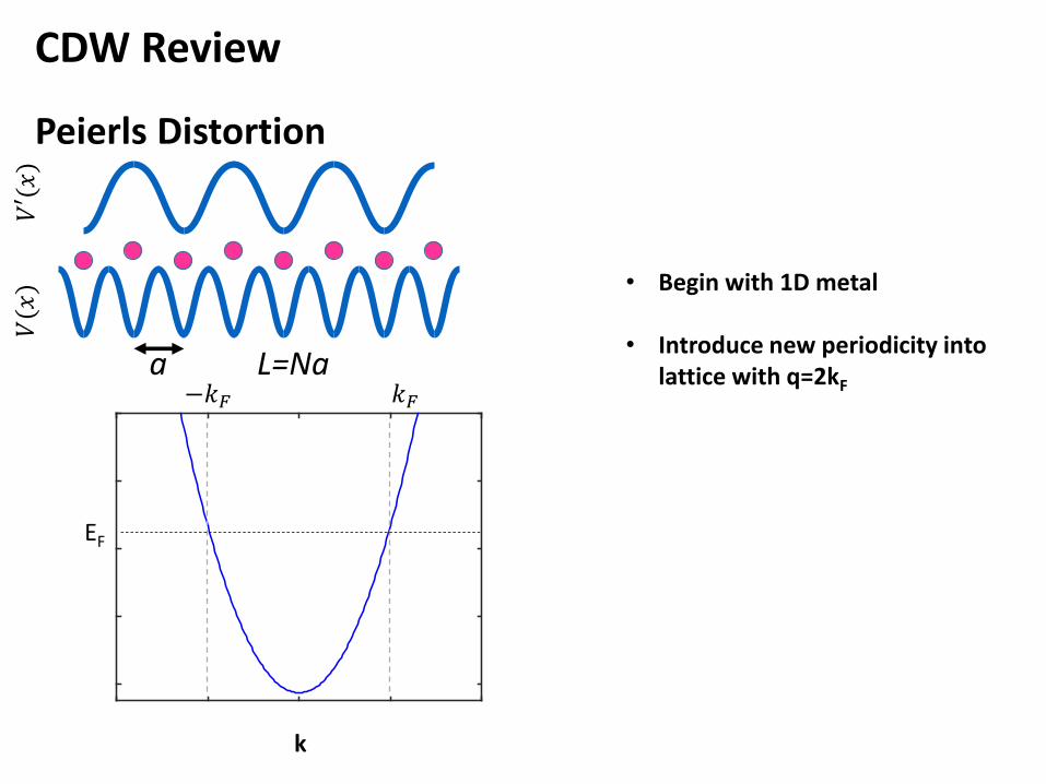
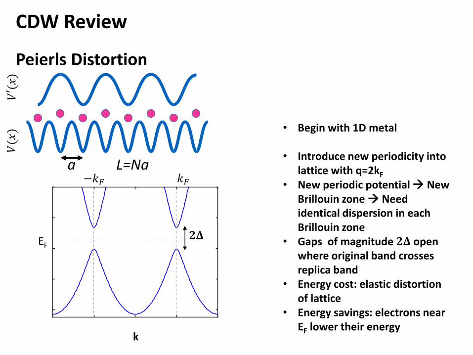
CDW Review
• Begin with 1D metal
• Introduce new periodicity into lattice with q=2kF
a
Peierls Distortion
𝑘𝐹−𝑘𝐹
𝑉(𝑥
)𝑉′(𝑥)
L=Na
k
EF

CDW Review
a
Peierls Distortion
𝑘𝐹−𝑘𝐹
𝑉(𝑥
)𝑉′(𝑥)
L=Na
k
EF
• Begin with 1D metal
• Introduce new periodicity into lattice with q=2kF
• New periodic potential New Brillouin zone Need identical dispersion in each Brillouin zone
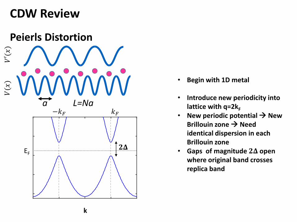
CDW Review
a
Peierls Distortion
𝑘𝐹−𝑘𝐹
𝑉(𝑥
)𝑉′(𝑥)
L=Na
• Begin with 1D metal
• Introduce new periodicity into lattice with q=2kF
• New periodic potential New Brillouin zone Need identical dispersion in each Brillouin zone
• Gaps of magnitude 𝟐𝚫 open where original band crosses replica band
𝟐𝚫
k
EF
CDW Review
a
Peierls Distortion
𝑘𝐹−𝑘𝐹
𝑉(𝑥
)𝑉′(𝑥)
L=Na
• Begin with 1D metal
• Introduce new periodicity into lattice with q=2kF
• New periodic potential New Brillouin zone Need identical dispersion in each Brillouin zone
• Gaps of magnitude 𝟐𝚫 open where original band crosses replica band
• Energy cost: elastic distortion of lattice
• Energy savings: electrons near EF lower their energy
𝟐𝚫
k
EF
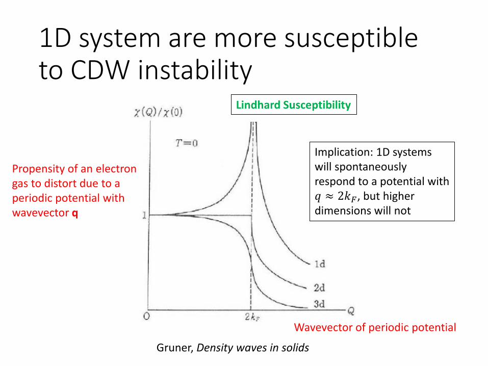
1D system are more susceptible to CDW instability
Gruner, Density waves in solids
Propensity of an electron gas to distort due to a periodic potential with wavevector q
Wavevector of periodic potential
Lindhard Susceptibility
Implication: 1D systems will spontaneously respond to a potential with 𝑞 ≈ 2𝑘𝐹, but higher dimensions will not

Nesting: how higher dimensional Fermi surfaces can effectively look 1D
1D FS in 1D space
k+kF
-kF
1D FS in 2D space
kx
ky
1D FS in 3D space
kx
ky
kz
Good candidates for electronically driven CDW have portions of FS which form parallel lines or sheets (i.e. are nested)
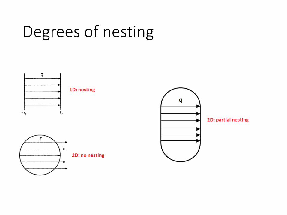
Degrees of nesting

Quick review of ARPES
k
EF
𝑘𝐹−𝑘𝐹
E-E F
Every electron in band structure has crystal momentum (k) and binding energy (𝐸𝐵)
k
|𝐸𝐵|Photon gives electron energy kick (ℎ𝜈) and negligible (for this course) momentum kick
(photo)electron loses work function (𝜙) worth of energy upon exiting material
Kinetic energy (𝐸𝑘𝑖𝑛) of photoelectron is detected, encoding original binding energy
𝐸𝑘𝑖𝑛 = ℎ𝜈 − 𝜙 − |𝐸𝐵|
Emission angle (𝜃) of photoelectron is simultaneously measured, encoding crystal momentum that electron had inside sample
ℏ𝒌 = 𝟐𝒎𝒆𝑬𝒌𝒊𝒏𝒔𝒊𝒏𝜽

ARPES resources
• Campuzano, Norman, Randeria. Photoemission in the high-Tc superconductors. https://arxiv.org/pdf/cond-mat/0209476.pdf Good for: matrix elements
• Damascelli, Hussain, Shen. Angle-resolved photoemission studies of the cuprate superconductors. Rev. Mod. Phys. 75 473 (2003)Good for: short review of formalism
• Damascelli. Probing the Electronic Structure of Complex Systems by ARPES. Physica Scripta. Vol. T109, 61–74, 2004 (https://www.cuso.ch/fileadmin/physique/document/Damascelli_ARPES_CUSO_2011_Lecture_Notes.pdf)Good for: information about kz and quantifying quasiparticle lifetimes
• Hufner, Photoelectron Spectroscopy, Springer (2003)Good for: Historical overview; formalism; broad review of technique

Case study: RTe3 (R=Tm, Er, Ho, Dy, Tb, Gd)
Ru et al. PRB 78, 012410 (2008)
Some members have two CDWs and some become superconducting under pressure
N. Ru thesishttp://web.stanford.edu/group/fisher/people/Nancy_Ru_thesis.pdf

How are CDWs usually discovered?
Ru et al. PRB 77, 035114 (2008)
(not the first resistivity measurement on this material)
Often discovered by transport
Why does resistivity show upturn just below TCDW?
Why is there metallic resistivity at low temperature?
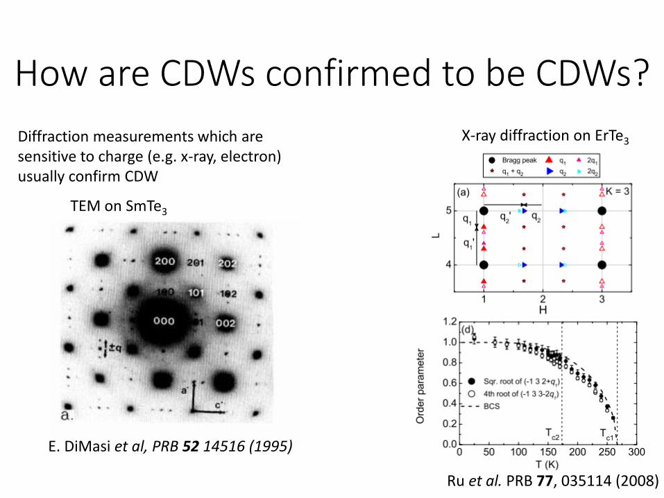
How are CDWs confirmed to be CDWs?
Diffraction measurements which are sensitive to charge (e.g. x-ray, electron) usually confirm CDW
TEM on SmTe3
E. DiMasi et al, PRB 52 14516 (1995)
X-ray diffraction on ErTe3
Ru et al. PRB 77, 035114 (2008)

What else is there to learn about CDW?• What causes it? (structurally or electronically
driven?)
• How does it nucleate?
• How much of the Fermi surface is involved?
• How large is the gap?
• What are its collective excitations?

A tale of two CDWs in ErTe3 (+ more practice reading ARPES data)
Moore et al. PRB 81, 073102 (2010)
kz
kx
Bright regions: remaining Fermi surface
Dark regions formerly occupied by Fermi surface: gapped out by CDW
Nesting wavevector
Fermi surface map produced by taking many parallel slices (E vs k), integrating over small energy window near EF, and interpolating slices together

What does the original FS look like?Good approximation can be achieved via tight-binding model(Tight binding model: electronic band structure approximated from overlap of atomic orbital on adjacent atoms)
Brouet et al. PRB 77, 235104 (2008)
• Fermi surface originates from Te p-orbitals and is almost 1D (small buckling because 𝑡⊥ ≠ 0
Yao et al. PRB 74, 245126 (2006)

What does the original FS look like?
• R/Te slab has lower symmetry than Te layer, making a larger unit cell (smaller Brillouin zone)
Folded FS
LTMO band structure calcRu et al. PRB 77, 035114 (2008)
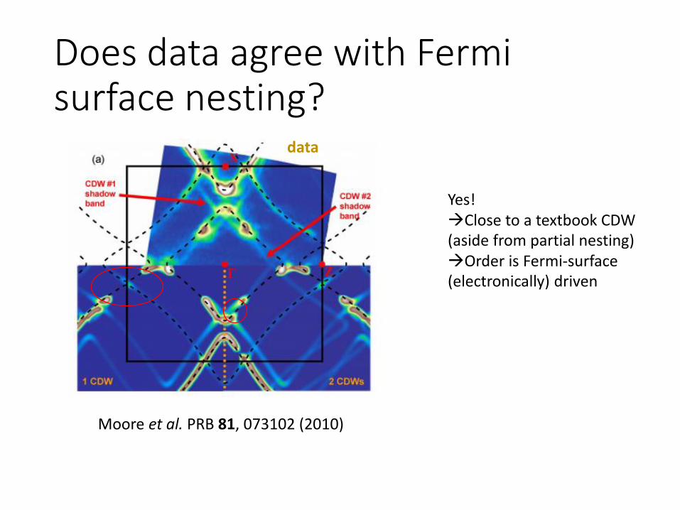
Does data agree with Fermi surface nesting?
Moore et al. PRB 81, 073102 (2010)
data
Yes!Close to a textbook CDW (aside from partial nesting)Order is Fermi-surface (electronically) driven

CDW order parameter
Complex order parameter:
Ψ~Δ𝑒𝑖𝜙
A
Image source: Torchinsky et al, Nat. Mater. (2013)
Amplitude (Δ)
Phase (𝜙)
What is an order parameter?The measure of the degree of order of a given phase. Typically zero above the ordering temperature
What measured/calculated quantities are related to the CDW order parameter?• Amount of lattice distortion• Amount of charge involved• Amplitude of satellite Bragg
peak• Magnitude of gap

Order parameter in ErTe3 (visualizing gaps in ARPES)
Method 1: Disappearance of intensity in fermi surface map (only works if gap opens at EF)
Method 2: Energy vs k dispersion
Method 2.5: Energy distribution curve (EDC) + reasonable definition of gap edge
Moore et al. PRB 81, 073102 (2010)

Extracting spectral gaps
1. Get rid of Fermi-Dirac cutoff by dividing by Fermi-Dirac distribution or symmetrizing (only if there is e-h symmetry)
2. Plot energy distribution curves (EDCs): intensity vs energy at fixed momentum
3. Quantify gap in reasonable way• Peak-to EF• Leading edge gap
(LEG)• Fit to model
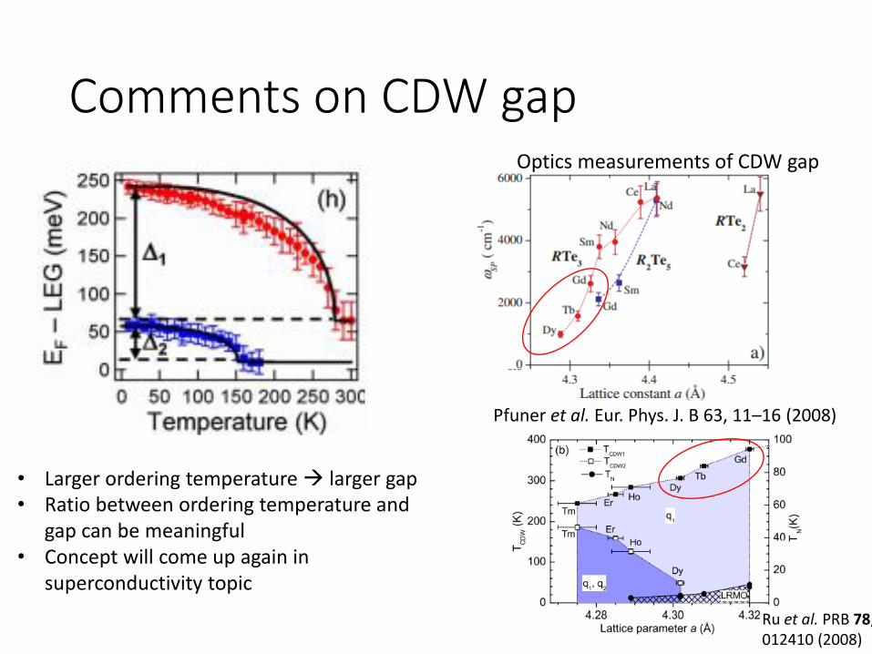
Comments on CDW gap
• Larger ordering temperature larger gap• Ratio between ordering temperature and
gap can be meaningful• Concept will come up again in
superconductivity topic
Optics measurements of CDW gap
Pfuner et al. Eur. Phys. J. B 63, 11–16 (2008)
Ru et al. PRB 78, 012410 (2008)

Another example: TbTe3
Schmitt et al, Science 321 (2008)
A. Fang et al. PRL 99, 046401 (2007)
Is there a gap here?-8
00
meV
-20
0 m
eV+2
00
meV

Consequences of imperfect nesting
Brouet et al. PRL 93 (2004)
Terminology:• Folded = extra bands from
larger 3D unit cell• Shadow = band from new
periodicity introduced by CDW (often called folded band in literature)
Perfect nesting
imperfect nesting
• If a portion of the FS is poorly nested, original band and ‘shadow’ band will intersect away from EF
• Gap will open at band crossing, but it will not be centered at EF
Density wave without nesting: gap not centered at EF

From “Density Waves in Solids” by George Gruner - 1994.
• The lattice vibrations at 𝑞𝐶𝐷𝑊 =
2𝑘𝐹 freeze in (also called softening)• This type of distortion is called a
Kohn anomaly• Electron-phonon coupling is
important to charge order if the lattice is involved in any way (leading, following, simultaneous)
What kind of phonon branch is this?
Electron-phonon coupling
Image source: https://en.wikipedia.org/wiki/Phonon

Kohn Anomaly in ZrTe3TCDW~63K
(Different crystal structure from RTe3 discussed thus far)
How to measure acoustic phonon branch?• Neutron scattering• Diffuse x-ray scattering
• Phonon softening at qCDW begins T>>TCDW
• Intensity of satellite Bragg peak begins to increase at the same q a bit above TCDW
Hoesch et al. PRL 102, 086402 (2009)
phonons electrons
From “Density Waves in Solids” by George Gruner - 1994.
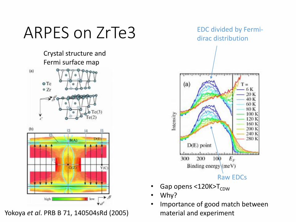
ARPES on ZrTe3Crystal structure and Fermi surface map
Raw EDCs
EDC divided by Fermi-dirac distribution
Yokoya et al. PRB B 71, 140504sRd (2005)
• Gap opens <120K>TCDW
• Why?• Importance of good match between
material and experiment
Resources on CDWs
• General overview of everything: Gruner, Density waves in solids (1994)
• Energetic of Peierls instability: Kittel, Solid State Physics, Ch14
• Recent review: P. Monceau, https://arxiv.org/pdf/1307.0929.pdf