Embed Size (px)
Citation preview
IEEE TRANSACTIONS ON POWER ELECTRONICS, VOL. 27, NO. 4, APRIL 2012 2067
Cascade Dual Buck Inverter With Phase-Shift ControlPengwei Sun, Student Member, IEEE, Chuang Liu, Student Member, IEEE, Jih-Sheng Lai, Fellow, IEEE,
and Chien-Liang Chen, Member, IEEE
Abstract—This paper presents a new type of cascade inverterbased on dual buck topology and phase-shift control scheme. Theproposed cascade dual buck inverter with phase-shift control in-herits all the merits of dual buck type inverters and overcomes someof their drawbacks. Compared to traditional cascade inverters, ithas much enhanced system reliability thanks to no shoot-throughproblems and lower switching loss with the help of using powerMOSFETs. With phase-shift control, it theoretically eliminates theinherent current zero-crossing distortion of the single-unit dualbuck type inverter. In addition, phase-shift control and cascadetopology can greatly reduce the ripple current or cut down thesize of passive components by increasing the equivalent switchingfrequency. A cascade dual buck inverter has been designed andtested to demonstrate the feasibility and advantages of the sys-tem by comparing single-unit dual buck inverter, 2-unit and 3-unitcascade dual buck inverters at the same 1 kW, 120 V ac outputconditions.
Index Terms—Cascade inverter, dual buck inverter, phase-shiftcontrol.
I. INTRODUCTION
AMONG various multilevel voltage-source inverters, themost commonly used and commercially available ones
are the neutral-point-clamped inverter, flying capacitor inverter,and cascade H-bridge inverter [1]–[4]. The cascade type in-verters are capable of reaching higher output voltage level byusing commercially standard lower voltage devices and compo-nents. They also feature a modular design concept which makesmaintenance less burdensome [1]–[10]. The cascade invertersare well suited for utility interface of various renewable en-ergy sources, such as photovoltaics, fuel cells, battery energystorage, and electric vehicle drives, where separate dc sourcesnaturally exist [11]–[21]. However, because most current cas-cade inverters are based on a series connection of several singlevoltage source inverters (VSI) with two active devices in oneleg, they suffer from shoot-through problems, the most domi-nating failure of VSI. In addition, for the hard-switched cascadeinverters operating at higher dc bus voltage, they lose the ben-efit of using power MOSFETs as the active switching devicesfor efficiency improvement and fast switching speed when theyare available at certain voltage and power level. For example,when the cell dc bus voltage goes up to 300 V to 600 V, high
Manuscript received March 11, 2011; revised June 22, 2011 and August 8,2011; accepted September 14, 2011. Date of current version February 20, 2012.Recommended for publication by Associate Editor S. Choi.
P. Sun, J.-S. Lai, and C.-L. Chen are with Virginia Tech, Blacksburg, VA24060 USA (e-mail: [email protected]; [email protected]; [email protected]).
C. Liu is with the Harbin Institute of Technology, Harbin 150001, China(e-mail: [email protected]).
Color versions of one or more of the figures in this paper are available onlineat http://ieeexplore.ieee.org.
Digital Object Identifier 10.1109/TPEL.2011.2169282
voltage power MOSFETs (600 V to 900 V level, like CoolMOSor MDmesh series) cannot be adopted to work at hard-switchedsituations like traditional cascade H-bridge inverters because ofthe reverse recovery issues of the body diode [34]–[38] unlesssoft-switching techniques are employed [39]–[41].
This paper proposes a new cascade dual buck inverter basedon single dual buck inverter topology to better address the issuesmentioned above. The dual buck type inverters are still VSI, butwith the unique topology and operation, they do not have theshoot-through worries, which leads to greatly enhanced relia-bility [22]–[24]. Thanks to the lack of shoot-through worries ofeach building block, the cascade dual buck inverter features im-proved system reliability compared to other cascade inverters. Inaddition, the cascade dual buck inverter does not have the deadtime related issues of conventional VSI-based cascade inverters,which can easily push the duty cycle to the theoretical limit andfully transfer the energy to load through total PWM. In addition,the cascade dual buck inverter can be hard-switched while uti-lizing the benefits of power MOSFETs at certain power levels.
Phase-shift control is widely used for cascade inverters be-cause it is easy to implement with digital controllers and itequivalently increases the switching frequency by the numberof cascade units, which reduces the output voltage and currentripple [25]–[27]. For the cascade dual buck inverter, phase-shift control is adopted as well. Besides the common benefits, itsolves another problem for this unique cascade topology. One ofthe inherent drawbacks of single dual buck inverters is the cur-rent zero-crossing distortion, which will be explained in detailin Section III. Fortunately, with the help of phase-shift control,cascade dual buck inverter theoretically eliminates the zero-crossing distortion from zero to full load conditions.
The paper first shows different topologies of the proposedcascade dual buck inverters and their operation principles. Thispaper takes single-phase cascade dual buck half-bridge inverteras the analytical and design subject to demonstrate the feasibilityand advantages of cascade dual buck inverters. The phase-shiftcontrol scheme is analyzed by comparing single-unit dual buckinverter and 2-unit cascade dual buck inverter. The closed-loopcontrol for cascade dual buck inverter has been designed andimplemented. A 1 kW, 120 V ac output cascade dual buckinverter system has been built to validate the proposed topologyand control by comparing the experimental test results of single-unit dual buck inverter, 2-unit and 3-unit cascade dual buckinverters.
II. TOPOLOGY AND OPERATION PRINCIPLE
The single-unit dual buck inverter has two basic forms, dualbuck half-bridge inverter [22], [24] and dual buck full-bridgeinverter [23]. The proposed cascade dual buck inverter has
0885-8993/$26.00 © 2011 IEEE
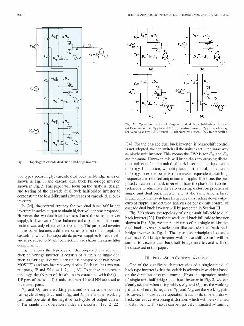
2068 IEEE TRANSACTIONS ON POWER ELECTRONICS, VOL. 27, NO. 4, APRIL 2012
Fig. 1. Topology of cascade dual buck half-bridge inverter.
two types accordingly: cascade dual buck half-bridge inverter,shown in Fig. 1, and cascade dual buck full-bridge inverter,shown in Fig. 3. This paper will focus on the analysis, design,and testing of the cascade dual buck half-bridge inverter todemonstrate the feasibility and advantages of cascade dual buckinverters.
In [24], the control strategy for two dual buck half-bridgeinverters in series output to obtain higher voltage was proposed.However, the two dual buck inverters shared the same dc powersupply, had two sets of filter inductor and capacitor, and the con-nection was only effective for two units. The proposed inverterin this paper features a different series connection concept, thecascading, which has separate dc power supplies for each cell,and is extended to N unit connection, and shares the same filtercomponents.
Fig. 1 shows the topology of the proposed cascade dualbuck half-bridge inverter. It consists of N units of single dualbuck half-bridge inverter. Each unit is composed of two powerMOSFETs and two fast recovery diodes. Each unit has two out-put ports, iP and iN (i = 1, 2, . . . , N ). To realize the cascadetopology, the iN port of the ith unit is connected with the (i +1)P port of the (i + 1)th unit, and port 1P and NN are used asthe output ports.
Sip and Dip are a working pair, and operate at the positivehalf-cycle of output current i. Sin and Din are another workingpair, and operate at the negative half-cycle of output currenti. The single unit operation modes are shown in Fig. 2 [22],
Fig. 2. Operation modes of single-unit dual buck half-bridge inverter.(a) Positive current, S1p turned ON. (b) Positive current, D1p free-wheeling.(c) Negative current, S1n turned ON. (d) Negative current, D1n free-wheeling.
[24]. For the cascade dual buck inverter, if phase-shift controlis not adopted, we can switch all the units exactly the same wayas single-unit inverter. This means the PWMs for Sip and Sinare the same. However, this will bring the zero-crossing distor-tion problem of single-unit dual buck inverters into the cascadetopology. In addition, without phase-shift control, the cascadetopology loses the benefits of increased equivalent switchingfrequency and reduced output current ripple. Therefore, the pro-posed cascade dual buck inverter utilizes the phase-shift controltechnique to eliminate the zero-crossing distortion problem ofsingle unit dual buck inverter and at the same time achievehigher equivalent switching frequency thus cutting down outputcurrent ripple. The detailed analysis of phase-shift control ofcascade dual buck inverter will be presented in Section III.
Fig. 3(a) shows the topology of single-unit full-bridge dualbuck inverter [23]. For the cascade dual buck full-bridge invertershown in Fig. 3(b), we can put N units of this single full-bridgedual buck inverter in series just like cascade dual buck half-bridge inverter in Fig. 1. The operation principle of cascadedual buck full-bridge inverter with phase-shift control will besimilar to cascade dual buck half-bridge inverter, and will notbe discussed in this paper.
III. PHASE-SHIFT CONTROL ANALYSIS
One of the significant characteristics of a single-unit dualbuck type inverter is that the switch is selectively working basedon the direction of output current. From the operation modesof single-unit half-bridge dual buck inverter in Fig. 2, we canclearly see that when i1 is positive, S1p and D1p are the workingpair, and when i1 is negative, S1n and D1n are the working pair.However, this distinctive operation leads to its inherent draw-back, current zero-crossing distortion, which will be explainedin detail below. This issue can be passively mitigated by turning
SUN et al.: CASCADE DUAL BUCK INVERTER WITH PHASE-SHIFT CONTROL 2069
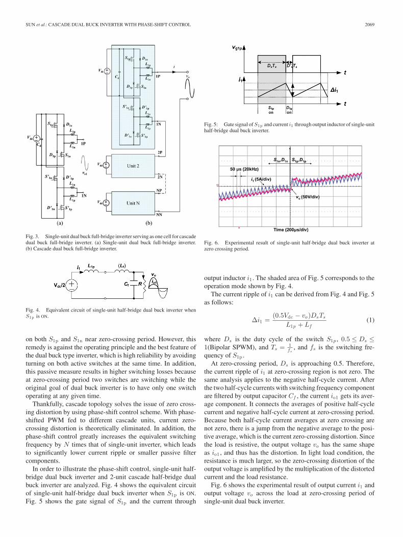
Fig. 3. Single-unit dual buck full-bridge inverter serving as one cell for cascadedual buck full-bridge inverter. (a) Single-unit dual buck full-bridge inverter.(b) Cascade dual buck full-bridge inverter.
Fig. 4. Equivalent circuit of single-unit half-bridge dual buck inverter whenS1p is ON.
on both S1p and S1n near zero-crossing period. However, thisremedy is against the operating principle and the best feature ofthe dual buck type inverter, which is high reliability by avoidingturning on both active switches at the same time. In addition,this passive measure results in higher switching losses becauseat zero-crossing period two switches are switching while theoriginal goal of dual buck inverter is to have only one switchoperating at any given time.
Thankfully, cascade topology solves the issue of zero cross-ing distortion by using phase-shift control scheme. With phase-shifted PWM fed to different cascade units, current zero-crossing distortion is theoretically eliminated. In addition, thephase-shift control greatly increases the equivalent switchingfrequency by N times that of single-unit inverter, which leadsto significantly lower current ripple or smaller passive filtercomponents.
In order to illustrate the phase-shift control, single-unit half-bridge dual buck inverter and 2-unit cascade half-bridge dualbuck inverter are analyzed. Fig. 4 shows the equivalent circuitof single-unit half-bridge dual buck inverter when S1p is ON.Fig. 5 shows the gate signal of S1p and the current through
Fig. 5: Gate signal of S1p and current i1 through output inductor of single-unithalf-bridge dual buck inverter.
Fig. 6. Experimental result of single-unit half-bridge dual buck inverter atzero crossing period.
output inductor i1 . The shaded area of Fig. 5 corresponds to theoperation mode shown by Fig. 4.
The current ripple of i1 can be derived from Fig. 4 and Fig. 5as follows:
Δi1 =(0.5Vdc − vo)DsTs
L1p + Lf(1)
where Ds is the duty cycle of the switch S1p , 0.5 ≤ Ds ≤1(Bipolar SPWM), and Ts = 1
fs, and fs is the switching fre-
quency of S1p .At zero-crossing period, Ds is approaching 0.5. Therefore,
the current ripple of i1 at zero-crossing region is not zero. Thesame analysis applies to the negative half-cycle current. Afterthe two half-cycle currents with switching frequency componentare filtered by output capacitor Cf , the current io1 gets its aver-age component. It connects the averages of positive half-cyclecurrent and negative half-cycle current at zero-crossing period.Because both half-cycle current averages at zero crossing arenot zero, there is a jump from the negative average to the posi-tive average, which is the current zero-crossing distortion. Sincethe load is resistive, the output voltage vo has the same shapeas io1 , and thus has the distortion. In light load condition, theresistance is much larger, so the zero-crossing distortion of theoutput voltage is amplified by the multiplication of the distortedcurrent and the load resistance.
Fig. 6 shows the experimental result of output current i1 andoutput voltage vo across the load at zero-crossing period ofsingle-unit dual buck inverter.
2070 IEEE TRANSACTIONS ON POWER ELECTRONICS, VOL. 27, NO. 4, APRIL 2012
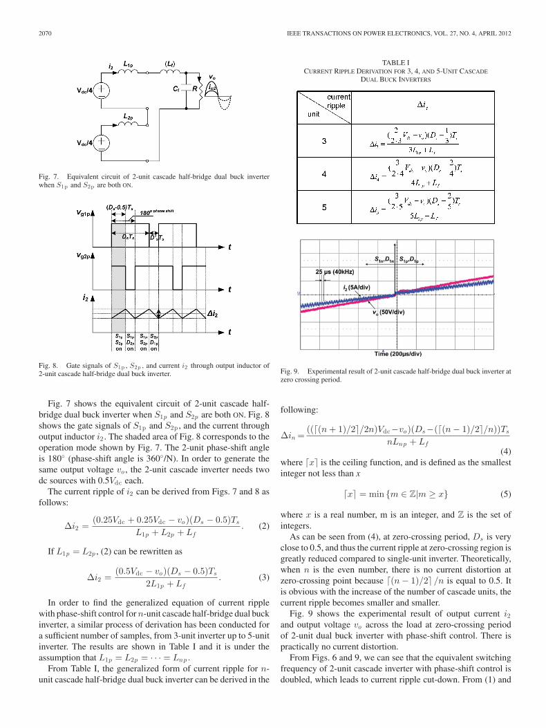
Fig. 7. Equivalent circuit of 2-unit cascade half-bridge dual buck inverterwhen S1p and S2p are both ON.
Fig. 8. Gate signals of S1p , S2p , and current i2 through output inductor of2-unit cascade half-bridge dual buck inverter.
Fig. 7 shows the equivalent circuit of 2-unit cascade half-bridge dual buck inverter when S1p and S2p are both ON. Fig. 8shows the gate signals of S1p and S2p , and the current throughoutput inductor i2 . The shaded area of Fig. 8 corresponds to theoperation mode shown by Fig. 7. The 2-unit phase-shift angleis 180◦ (phase-shift angle is 360◦/N). In order to generate thesame output voltage vo , the 2-unit cascade inverter needs twodc sources with 0.5Vdc each.
The current ripple of i2 can be derived from Figs. 7 and 8 asfollows:
Δi2 =(0.25Vdc + 0.25Vdc − vo)(Ds − 0.5)Ts
L1p + L2p + Lf. (2)
If L1p = L2p , (2) can be rewritten as
Δi2 =(0.5Vdc − vo)(Ds − 0.5)Ts
2L1p + Lf. (3)
In order to find the generalized equation of current ripplewith phase-shift control for n-unit cascade half-bridge dual buckinverter, a similar process of derivation has been conducted fora sufficient number of samples, from 3-unit inverter up to 5-unitinverter. The results are shown in Table I and it is under theassumption that L1p = L2p = · · · = Lnp .
From Table I, the generalized form of current ripple for n-unit cascade half-bridge dual buck inverter can be derived in the
TABLE ICURRENT RIPPLE DERIVATION FOR 3, 4, AND 5-UNIT CASCADE
DUAL BUCK INVERTERS
Fig. 9. Experimental result of 2-unit cascade half-bridge dual buck inverter atzero crossing period.
following:
Δin =((�(n + 1)/2�/2n)Vdc−vo)(Ds−(�(n − 1)/2�/n))Ts
nLnp + Lf
(4)where �x� is the ceiling function, and is defined as the smallestinteger not less than x
�x� = min {m ∈ Z|m ≥ x} (5)
where x is a real number, m is an integer, and Z is the set ofintegers.
As can be seen from (4), at zero-crossing period, Ds is veryclose to 0.5, and thus the current ripple at zero-crossing region isgreatly reduced compared to single-unit inverter. Theoretically,when n is the even number, there is no current distortion atzero-crossing point because �(n − 1)/2� /n is equal to 0.5. Itis obvious with the increase of the number of cascade units, thecurrent ripple becomes smaller and smaller.
Fig. 9 shows the experimental result of output current i2and output voltage vo across the load at zero-crossing periodof 2-unit dual buck inverter with phase-shift control. There ispractically no current distortion.
From Figs. 6 and 9, we can see that the equivalent switchingfrequency of 2-unit cascade inverter with phase-shift control isdoubled, which leads to current ripple cut-down. From (1) and
SUN et al.: CASCADE DUAL BUCK INVERTER WITH PHASE-SHIFT CONTROL 2071
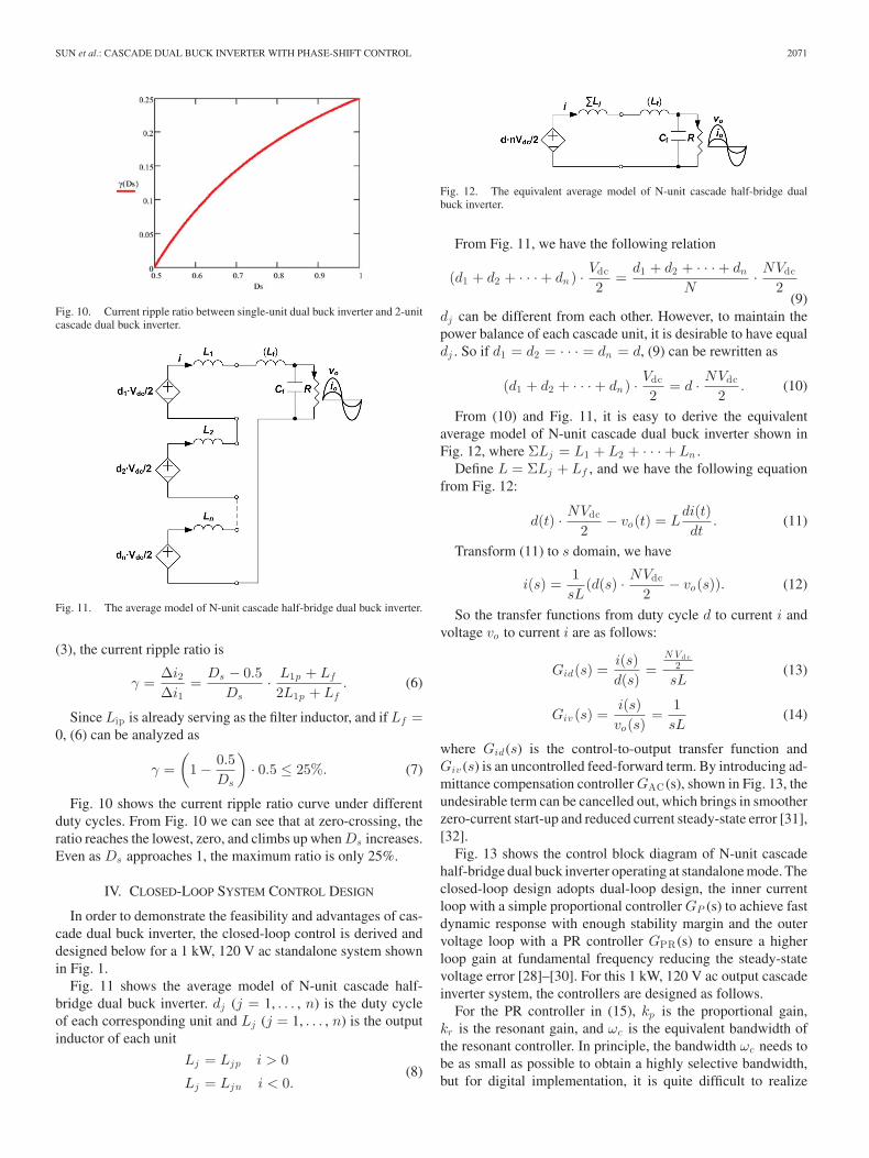
Fig. 10. Current ripple ratio between single-unit dual buck inverter and 2-unitcascade dual buck inverter.
Fig. 11. The average model of N-unit cascade half-bridge dual buck inverter.
(3), the current ripple ratio is
γ =Δi2Δi1
=Ds − 0.5
Ds· L1p + Lf
2L1p + Lf. (6)
Since Lip is already serving as the filter inductor, and if Lf =0, (6) can be analyzed as
γ =(
1 − 0.5Ds
)· 0.5 ≤ 25%. (7)
Fig. 10 shows the current ripple ratio curve under differentduty cycles. From Fig. 10 we can see that at zero-crossing, theratio reaches the lowest, zero, and climbs up when Ds increases.Even as Ds approaches 1, the maximum ratio is only 25%.
IV. CLOSED-LOOP SYSTEM CONTROL DESIGN
In order to demonstrate the feasibility and advantages of cas-cade dual buck inverter, the closed-loop control is derived anddesigned below for a 1 kW, 120 V ac standalone system shownin Fig. 1.
Fig. 11 shows the average model of N-unit cascade half-bridge dual buck inverter. dj (j = 1, . . . , n) is the duty cycleof each corresponding unit and Lj (j = 1, . . . , n) is the outputinductor of each unit
Lj = Ljp i > 0
Lj = Ljn i < 0.(8)
Fig. 12. The equivalent average model of N-unit cascade half-bridge dualbuck inverter.
From Fig. 11, we have the following relation
(d1 + d2 + · · · + dn ) · Vdc
2=
d1 + d2 + · · · + dn
N· NVdc
2(9)
dj can be different from each other. However, to maintain thepower balance of each cascade unit, it is desirable to have equaldj . So if d1 = d2 = · · · = dn = d, (9) can be rewritten as
(d1 + d2 + · · · + dn ) · Vdc
2= d · NVdc
2. (10)
From (10) and Fig. 11, it is easy to derive the equivalentaverage model of N-unit cascade dual buck inverter shown inFig. 12, where ΣLj = L1 + L2 + · · · + Ln .
Define L = ΣLj + Lf , and we have the following equationfrom Fig. 12:
d(t) · NVdc
2− vo(t) = L
di(t)dt
. (11)
Transform (11) to s domain, we have
i(s) =1sL
(d(s) · NVdc
2− vo(s)). (12)
So the transfer functions from duty cycle d to current i andvoltage vo to current i are as follows:
Gid(s) =i(s)d(s)
=N Vd c
2
sL(13)
Giv (s) =i(s)vo(s)
=1sL
(14)
where Gid (s) is the control-to-output transfer function andGiv (s) is an uncontrolled feed-forward term. By introducing ad-mittance compensation controller GAC (s), shown in Fig. 13, theundesirable term can be cancelled out, which brings in smootherzero-current start-up and reduced current steady-state error [31],[32].
Fig. 13 shows the control block diagram of N-unit cascadehalf-bridge dual buck inverter operating at standalone mode. Theclosed-loop design adopts dual-loop design, the inner currentloop with a simple proportional controller GP (s) to achieve fastdynamic response with enough stability margin and the outervoltage loop with a PR controller GPR (s) to ensure a higherloop gain at fundamental frequency reducing the steady-statevoltage error [28]–[30]. For this 1 kW, 120 V ac output cascadeinverter system, the controllers are designed as follows.
For the PR controller in (15), kp is the proportional gain,kr is the resonant gain, and ωc is the equivalent bandwidth ofthe resonant controller. In principle, the bandwidth ωc needs tobe as small as possible to obtain a highly selective bandwidth,but for digital implementation, it is quite difficult to realize
2072 IEEE TRANSACTIONS ON POWER ELECTRONICS, VOL. 27, NO. 4, APRIL 2012
Fig. 13. Control block diagram of N-unit cascade half-bridge dual buck inverter operating at standalone mode.
a small ωc . The controller gain at fundamental frequency canbe increased by increasing either kp or kr . On the other hand,kp and kr cannot be too high because this will impair systemstability [29], [30], [42]. With all the considerations above, theparameters for PR controller in this design have been chosen as
GPR(s) = kp +2ωckrs
s2 + 2ωcs + ω21
(15)
where kp = 0.02, kr = 12, ωc = 10.A current loop in a dual-loop system is designed to have a
high loop bandwidth with enough stability margin rather thanto reduce the current steady-state error by providing a highgain at fundamental frequency [42]. In this design, a simpleproportional controller will meet the requirement
GP (s) = 0.05. (16)
In [32], the equivalent dc bus voltage is Vdc for single unitinverter system, and thus the outcome of admittance compensa-tion term is the reciprocal of Vdc . From Fig. 13, we can clearlysee that the equivalent dc bus voltage for the cascade dual-buckinverter is NVdc/2. Therefore, the admittance compensationtransfer function is obtained as follows:
GAC(s) =1
NVdc/2(17)
In order to close the outer voltage loop, shown in Fig. 13,Gvi(s) is derived below based on the model in Fig. 12
Gvi(s) =1
sCf + 1/R. (18)
GLPF (s) is second-order low pass filter with cut-off frequency5 kHz and a damping ratio 0.7.
With the designed controllers above, the Bode plot of bothcompensated inner current loop gain and compensated outervoltage loop gain is shown in Fig. 14. As can be seen, thecurrent loop has the cross-over frequency 1.2 kHz with gainmargin 15.3 dB and phase margin 70.7◦. The voltage loop hasthe cross-over frequency 209 Hz with phase margin 87.2◦, andat 60 Hz fundamental frequency it has a gain of 35.5 dB to rejectthe steady state error.
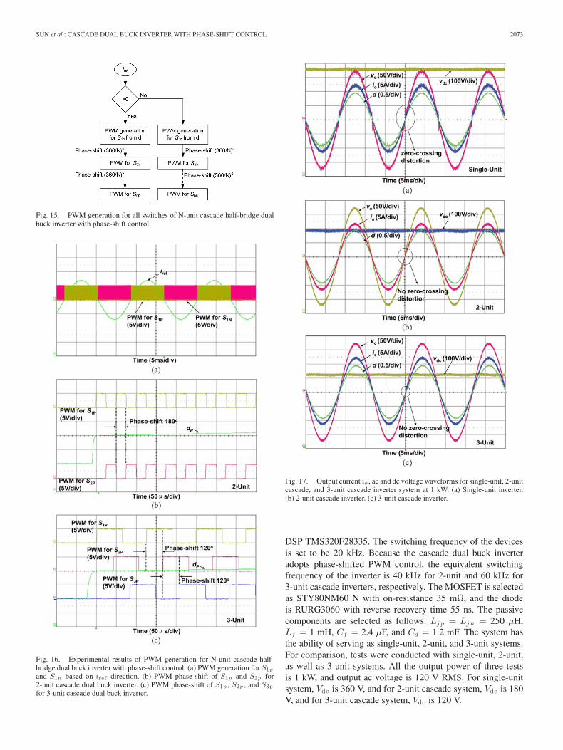
Fig. 15 shows the PWM generation flow chart based on thecurrent reference signal from Fig. 13. Fig. 16 shows the experi-mental results for PWM generation based on the sequence fromFig. 15. It can be seen that the PWMs for Sip and Sin neveroverlap, which means this cascade dual buck inverter is shoot-
Fig. 14. Bode plot of compensated inner current loop gain and outer voltageloop gain. (a) Bode plot of compensated current loop gain. (b) Bode plot ofcompensated voltage loop gain.
through free. The phase-shifted PWMs are simple to implementby digital controller by just adding an incremental angle to theadjacent cascade unit.
V. COMPARATIVE EXPERIMENTAL RESULTS
To prove the viability and merits of the proposed cascadedual buck inverter with phase-shift control, a 1 kW, 120 V acoutput cascade dual buck half-bridge inverter system in stan-dalone operation was designed and tested. The system structureof the experiment is the same as in Fig. 1, and the controlscheme applied is shown in Figs. 13 and 15. The system con-troller and PWM generation are conducted by TI floating point
SUN et al.: CASCADE DUAL BUCK INVERTER WITH PHASE-SHIFT CONTROL 2073
Fig. 15. PWM generation for all switches of N-unit cascade half-bridge dualbuck inverter with phase-shift control.
Fig. 16. Experimental results of PWM generation for N-unit cascade half-bridge dual buck inverter with phase-shift control. (a) PWM generation for S1p
and S1n based on iref direction. (b) PWM phase-shift of S1p and S2p for2-unit cascade dual buck inverter. (c) PWM phase-shift of S1p , S2p , and S3pfor 3-unit cascade dual buck inverter.
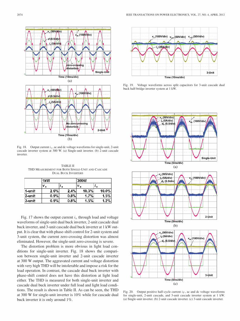
Fig. 17. Output current io , ac and dc voltage waveforms for single-unit, 2-unitcascade, and 3-unit cascade inverter system at 1 kW. (a) Single-unit inverter.(b) 2-unit cascade inverter. (c) 3-unit cascade inverter.
DSP TMS320F28335. The switching frequency of the devicesis set to be 20 kHz. Because the cascade dual buck inverteradopts phase-shifted PWM control, the equivalent switchingfrequency of the inverter is 40 kHz for 2-unit and 60 kHz for3-unit cascade inverters, respectively. The MOSFET is selectedas STY80NM60 N with on-resistance 35 mΩ, and the diodeis RURG3060 with reverse recovery time 55 ns. The passivecomponents are selected as follows: Lj p = Lj n = 250 μH,Lf = 1 mH, Cf = 2.4 μF, and Cd = 1.2 mF. The system hasthe ability of serving as single-unit, 2-unit, and 3-unit systems.For comparison, tests were conducted with single-unit, 2-unit,as well as 3-unit systems. All the output power of three testsis 1 kW, and output ac voltage is 120 V RMS. For single-unitsystem, Vdc is 360 V, and for 2-unit cascade system, Vdc is 180V, and for 3-unit cascade system, Vdc is 120 V.
2074 IEEE TRANSACTIONS ON POWER ELECTRONICS, VOL. 27, NO. 4, APRIL 2012
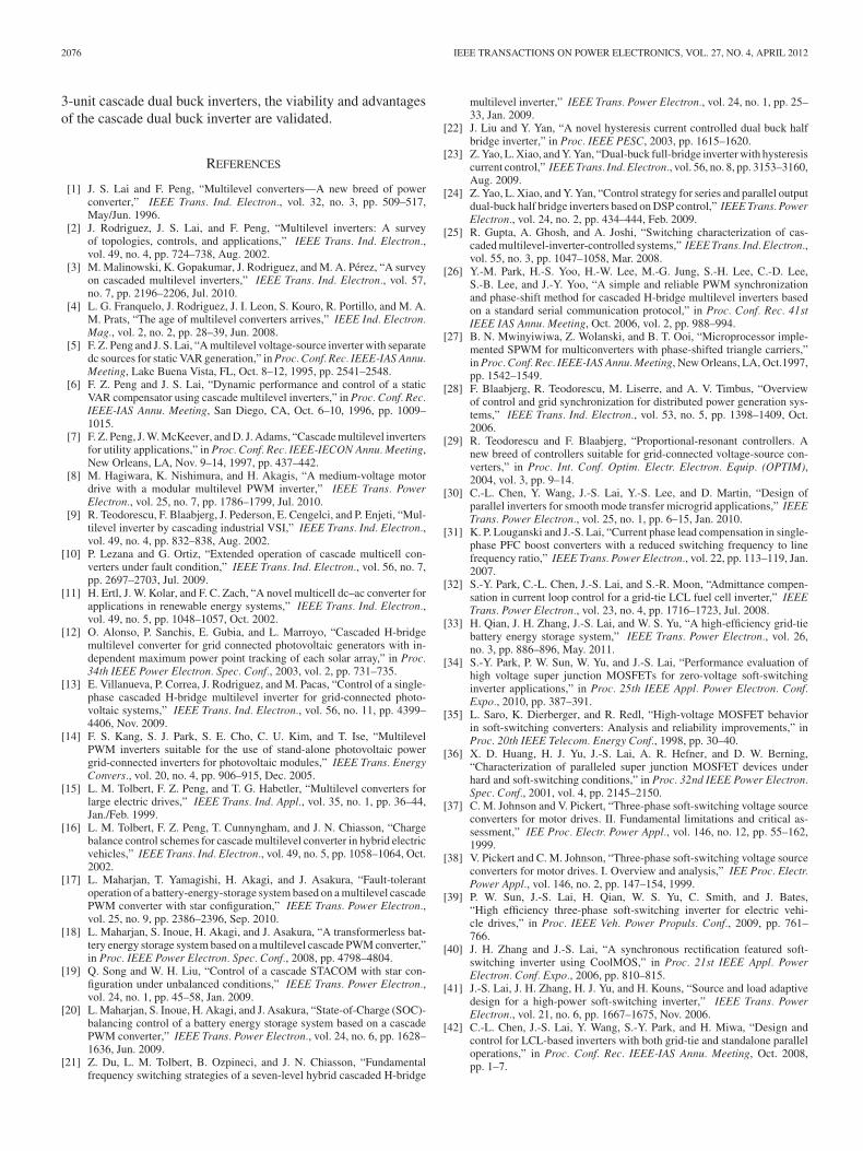
Fig. 18. Output current io , ac and dc voltage waveforms for single-unit, 2-unitcascade inverter system at 300 W. (a) Single-unit inverter. (b) 2-unit cascadeinverter.
TABLE IITHD MEASUREMENT FOR BOTH SINGLE-UNIT AND CASCADE
DUAL BUCK INVERTERS
Fig. 17 shows the output current io through load and voltagewaveforms of single-unit dual buck inverter, 2-unit cascade dualbuck inverter, and 3-unit cascade dual buck inverter at 1 kW out-put. It is clear that with phase-shift control for 2-unit system and3-unit system, the current zero-crossing distortion was almosteliminated. However, the single-unit zero-crossing is severe.
The distortion problem is more obvious in light load con-ditions for single-unit inverter. Fig. 18 shows the compari-son between single-unit inverter and 2-unit cascade inverterat 300 W output. The aggravated current and voltage distortionwith very high THD will be intolerable and impose a risk for theload operation. In contrast, the cascade dual buck inverter withphase-shift control does not have this distortion at light loadeither. The THD is measured for both single-unit inverter andcascade dual buck inverter under full load and light load condi-tions. The result is shown in Table II. As can be seen, the THDat 300 W for single-unit inverter is 10% while for cascade dualbuck inverter it is only around 1%.
Fig. 19. Voltage waveforms across split capacitors for 3-unit cascade dualbuck half-bridge inverter system at 1 kW.
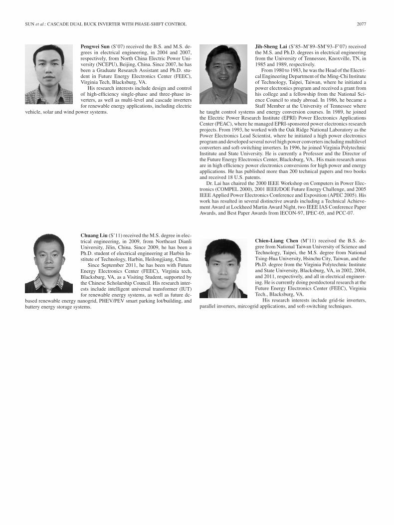
Fig. 20. Output positive half-cycle current iP , ac and dc voltage waveformsfor single-unit, 2-unit cascade, and 3-unit cascade inverter system at 1 kW.(a) Single-unit inverter. (b) 2-unit cascade inverter. (c) 3-unit cascade inverter.

SUN et al.: CASCADE DUAL BUCK INVERTER WITH PHASE-SHIFT CONTROL 2075
Fig. 21. Load step-up and step-down tests for single-unit inverter and 3-unitcascade inverter system. (a) Load step-up test for single-unit inverter. (b) Loadstep-down test for single-unit inverter. (c) Load step-up test for 3-unit cascadeinverter. (d) Load step-down test for 3-unit cascade inverter.
Fig. 19 shows the voltage vcd1 and vcd2 across the split ca-pacitors from one cell of 3-unit cascade dual buck half-bridgeinverter. For the cascade dual buck half-bridge inverter, the splitcapacitors are needed for each cascade unit. It can be seen that
Fig. 22. Efficiency measurement under different power output conditions.
the voltage of the capacitors is naturally balanced. In some cases,if the voltage across the capacitors is unbalanced, due to use ofdifferent types of capacitors, different ESR or other factors, avoltage balance compensator might be considered [33] to solvethe issue. The cascade dual buck full-bridge inverter is a bet-ter alternative to save two split capacitors and totally avoid theissue.
Fig. 20 shows the positive half cycle output current ipthrough inductor and voltage waveforms of single-unit dual buckinverter, 2-unit cascade dual buck inverter and 3-unit cascadedual buck inverter. dp is the duty cycle for current positive half-cycle. This shows the unique operating feature of single-unitdual buck inverter is inherited by cascade dual buck inverter.Every dual buck unit in the cascade system maintains the no-shoot-through characteristic, and thus leads to a more robust andreliable cascade inverter system than traditional voltage sourcebased cascade inverter.
Fig. 21 shows the output current and voltage waveforms ofsingle-unit inverter and 3-unit cascade dual buck inverter underload step conditions. Load step-up and step-down tests weredone to show the fast dynamics and good stability of the de-signed control system for cascade dual buck inverter. Eventhough single-unit system can withstand load change, its in-herent zero-crossing distortion will affect the control systemand be harmful to the load.
Fig. 22 shows the measured efficiency curve under differ-ent power output conditions for cascade dual buck half-bridgeinverter.
VI. CONCLUSION
A new series of cascade dual buck inverters has been proposedbased on single-unit dual buck inverters. The cascade dual buckinverter has all the merits of traditional cascade inverters, andimproves on its reliability by eliminating shoot-through wor-ries and dead-time concerns. With the adoption of phase-shiftcontrol, the cascade dual buck inverter solves the inherent cur-rent zero-crossing distortion problem of single-unit dual buckinverter.
To prove the effectiveness of the proposed topology and con-trol scheme, a cascade dual buck half-bridge inverter systemoperating at standalone mode with 1 kW, 120 V ac output ca-pability has been designed and tested. By comparison of exper-imental results of single-unit dual buck inverter with 2-unit and
2076 IEEE TRANSACTIONS ON POWER ELECTRONICS, VOL. 27, NO. 4, APRIL 2012
3-unit cascade dual buck inverters, the viability and advantagesof the cascade dual buck inverter are validated.
REFERENCES
[1] J. S. Lai and F. Peng, “Multilevel converters—A new breed of powerconverter,” IEEE Trans. Ind. Electron., vol. 32, no. 3, pp. 509–517,May/Jun. 1996.
[2] J. Rodriguez, J. S. Lai, and F. Peng, “Multilevel inverters: A surveyof topologies, controls, and applications,” IEEE Trans. Ind. Electron.,vol. 49, no. 4, pp. 724–738, Aug. 2002.
[3] M. Malinowski, K. Gopakumar, J. Rodriguez, and M. A. Perez, “A surveyon cascaded multilevel inverters,” IEEE Trans. Ind. Electron., vol. 57,no. 7, pp. 2196–2206, Jul. 2010.
[4] L. G. Franquelo, J. Rodriguez, J. I. Leon, S. Kouro, R. Portillo, and M. A.M. Prats, “The age of multilevel converters arrives,” IEEE Ind. Electron.Mag., vol. 2, no. 2, pp. 28–39, Jun. 2008.
[5] F. Z. Peng and J. S. Lai, “A multilevel voltage-source inverter with separatedc sources for static VAR generation,” in Proc. Conf. Rec. IEEE-IAS Annu.Meeting, Lake Buena Vista, FL, Oct. 8–12, 1995, pp. 2541–2548.
[6] F. Z. Peng and J. S. Lai, “Dynamic performance and control of a staticVAR compensator using cascade multilevel inverters,” in Proc. Conf. Rec.IEEE-IAS Annu. Meeting, San Diego, CA, Oct. 6–10, 1996, pp. 1009–1015.
[7] F. Z. Peng, J. W. McKeever, and D. J. Adams, “Cascade multilevel invertersfor utility applications,” in Proc. Conf. Rec. IEEE-IECON Annu. Meeting,New Orleans, LA, Nov. 9–14, 1997, pp. 437–442.
[8] M. Hagiwara, K. Nishimura, and H. Akagis, “A medium-voltage motordrive with a modular multilevel PWM inverter,” IEEE Trans. PowerElectron., vol. 25, no. 7, pp. 1786–1799, Jul. 2010.
[9] R. Teodorescu, F. Blaabjerg, J. Pederson, E. Cengelci, and P. Enjeti, “Mul-tilevel inverter by cascading industrial VSI,” IEEE Trans. Ind. Electron.,vol. 49, no. 4, pp. 832–838, Aug. 2002.
[10] P. Lezana and G. Ortiz, “Extended operation of cascade multicell con-verters under fault condition,” IEEE Trans. Ind. Electron., vol. 56, no. 7,pp. 2697–2703, Jul. 2009.
[11] H. Ertl, J. W. Kolar, and F. C. Zach, “A novel multicell dc–ac converter forapplications in renewable energy systems,” IEEE Trans. Ind. Electron.,vol. 49, no. 5, pp. 1048–1057, Oct. 2002.
[12] O. Alonso, P. Sanchis, E. Gubia, and L. Marroyo, “Cascaded H-bridgemultilevel converter for grid connected photovoltaic generators with in-dependent maximum power point tracking of each solar array,” in Proc.34th IEEE Power Electron. Spec. Conf., 2003, vol. 2, pp. 731–735.
[13] E. Villanueva, P. Correa, J. Rodriguez, and M. Pacas, “Control of a single-phase cascaded H-bridge multilevel inverter for grid-connected photo-voltaic systems,” IEEE Trans. Ind. Electron., vol. 56, no. 11, pp. 4399–4406, Nov. 2009.
[14] F. S. Kang, S. J. Park, S. E. Cho, C. U. Kim, and T. Ise, “MultilevelPWM inverters suitable for the use of stand-alone photovoltaic powergrid-connected inverters for photovoltaic modules,” IEEE Trans. EnergyConvers., vol. 20, no. 4, pp. 906–915, Dec. 2005.
[15] L. M. Tolbert, F. Z. Peng, and T. G. Habetler, “Multilevel converters forlarge electric drives,” IEEE Trans. Ind. Appl., vol. 35, no. 1, pp. 36–44,Jan./Feb. 1999.
[16] L. M. Tolbert, F. Z. Peng, T. Cunnyngham, and J. N. Chiasson, “Chargebalance control schemes for cascade multilevel converter in hybrid electricvehicles,” IEEE Trans. Ind. Electron., vol. 49, no. 5, pp. 1058–1064, Oct.2002.
[17] L. Maharjan, T. Yamagishi, H. Akagi, and J. Asakura, “Fault-tolerantoperation of a battery-energy-storage system based on a multilevel cascadePWM converter with star configuration,” IEEE Trans. Power Electron.,vol. 25, no. 9, pp. 2386–2396, Sep. 2010.
[18] L. Maharjan, S. Inoue, H. Akagi, and J. Asakura, “A transformerless bat-tery energy storage system based on a multilevel cascade PWM converter,”in Proc. IEEE Power Electron. Spec. Conf., 2008, pp. 4798–4804.
[19] Q. Song and W. H. Liu, “Control of a cascade STACOM with star con-figuration under unbalanced conditions,” IEEE Trans. Power Electron.,vol. 24, no. 1, pp. 45–58, Jan. 2009.
[20] L. Maharjan, S. Inoue, H. Akagi, and J. Asakura, “State-of-Charge (SOC)-balancing control of a battery energy storage system based on a cascadePWM converter,” IEEE Trans. Power Electron., vol. 24, no. 6, pp. 1628–1636, Jun. 2009.
[21] Z. Du, L. M. Tolbert, B. Ozpineci, and J. N. Chiasson, “Fundamentalfrequency switching strategies of a seven-level hybrid cascaded H-bridge
multilevel inverter,” IEEE Trans. Power Electron., vol. 24, no. 1, pp. 25–33, Jan. 2009.
[22] J. Liu and Y. Yan, “A novel hysteresis current controlled dual buck halfbridge inverter,” in Proc. IEEE PESC, 2003, pp. 1615–1620.
[23] Z. Yao, L. Xiao, and Y. Yan, “Dual-buck full-bridge inverter with hysteresiscurrent control,” IEEE Trans. Ind. Electron., vol. 56, no. 8, pp. 3153–3160,Aug. 2009.
[24] Z. Yao, L. Xiao, and Y. Yan, “Control strategy for series and parallel outputdual-buck half bridge inverters based on DSP control,” IEEE Trans. PowerElectron., vol. 24, no. 2, pp. 434–444, Feb. 2009.
[25] R. Gupta, A. Ghosh, and A. Joshi, “Switching characterization of cas-caded multilevel-inverter-controlled systems,” IEEE Trans. Ind. Electron.,vol. 55, no. 3, pp. 1047–1058, Mar. 2008.
[26] Y.-M. Park, H.-S. Yoo, H.-W. Lee, M.-G. Jung, S.-H. Lee, C.-D. Lee,S.-B. Lee, and J.-Y. Yoo, “A simple and reliable PWM synchronizationand phase-shift method for cascaded H-bridge multilevel inverters basedon a standard serial communication protocol,” in Proc. Conf. Rec. 41stIEEE IAS Annu. Meeting, Oct. 2006, vol. 2, pp. 988–994.
[27] B. N. Mwinyiwiwa, Z. Wolanski, and B. T. Ooi, “Microprocessor imple-mented SPWM for multiconverters with phase-shifted triangle carriers,”in Proc. Conf. Rec. IEEE-IAS Annu. Meeting, New Orleans, LA, Oct.1997,pp. 1542–1549.
[28] F. Blaabjerg, R. Teodorescu, M. Liserre, and A. V. Timbus, “Overviewof control and grid synchronization for distributed power generation sys-tems,” IEEE Trans. Ind. Electron., vol. 53, no. 5, pp. 1398–1409, Oct.2006.
[29] R. Teodorescu and F. Blaabjerg, “Proportional-resonant controllers. Anew breed of controllers suitable for grid-connected voltage-source con-verters,” in Proc. Int. Conf. Optim. Electr. Electron. Equip. (OPTIM),2004, vol. 3, pp. 9–14.
[30] C.-L. Chen, Y. Wang, J.-S. Lai, Y.-S. Lee, and D. Martin, “Design ofparallel inverters for smooth mode transfer microgrid applications,” IEEETrans. Power Electron., vol. 25, no. 1, pp. 6–15, Jan. 2010.
[31] K. P. Louganski and J.-S. Lai, “Current phase lead compensation in single-phase PFC boost converters with a reduced switching frequency to linefrequency ratio,” IEEE Trans. Power Electron., vol. 22, pp. 113–119, Jan.2007.
[32] S.-Y. Park, C.-L. Chen, J.-S. Lai, and S.-R. Moon, “Admittance compen-sation in current loop control for a grid-tie LCL fuel cell inverter,” IEEETrans. Power Electron., vol. 23, no. 4, pp. 1716–1723, Jul. 2008.
[33] H. Qian, J. H. Zhang, J.-S. Lai, and W. S. Yu, “A high-efficiency grid-tiebattery energy storage system,” IEEE Trans. Power Electron., vol. 26,no. 3, pp. 886–896, May. 2011.
[34] S.-Y. Park, P. W. Sun, W. Yu, and J.-S. Lai, “Performance evaluation ofhigh voltage super junction MOSFETs for zero-voltage soft-switchinginverter applications,” in Proc. 25th IEEE Appl. Power Electron. Conf.Expo., 2010, pp. 387–391.
[35] L. Saro, K. Dierberger, and R. Redl, “High-voltage MOSFET behaviorin soft-switching converters: Analysis and reliability improvements,” inProc. 20th IEEE Telecom. Energy Conf., 1998, pp. 30–40.
[36] X. D. Huang, H. J. Yu, J.-S. Lai, A. R. Hefner, and D. W. Berning,“Characterization of paralleled super junction MOSFET devices underhard and soft-switching conditions,” in Proc. 32nd IEEE Power Electron.Spec. Conf., 2001, vol. 4, pp. 2145–2150.
[37] C. M. Johnson and V. Pickert, “Three-phase soft-switching voltage sourceconverters for motor drives. II. Fundamental limitations and critical as-sessment,” IEE Proc. Electr. Power Appl., vol. 146, no. 12, pp. 55–162,1999.
[38] V. Pickert and C. M. Johnson, “Three-phase soft-switching voltage sourceconverters for motor drives. I. Overview and analysis,” IEE Proc. Electr.Power Appl., vol. 146, no. 2, pp. 147–154, 1999.
[39] P. W. Sun, J.-S. Lai, H. Qian, W. S. Yu, C. Smith, and J. Bates,“High efficiency three-phase soft-switching inverter for electric vehi-cle drives,” in Proc. IEEE Veh. Power Propuls. Conf., 2009, pp. 761–766.
[40] J. H. Zhang and J.-S. Lai, “A synchronous rectification featured soft-switching inverter using CoolMOS,” in Proc. 21st IEEE Appl. PowerElectron. Conf. Expo., 2006, pp. 810–815.
[41] J.-S. Lai, J. H. Zhang, H. J. Yu, and H. Kouns, “Source and load adaptivedesign for a high-power soft-switching inverter,” IEEE Trans. PowerElectron., vol. 21, no. 6, pp. 1667–1675, Nov. 2006.
[42] C.-L. Chen, J.-S. Lai, Y. Wang, S.-Y. Park, and H. Miwa, “Design andcontrol for LCL-based inverters with both grid-tie and standalone paralleloperations,” in Proc. Conf. Rec. IEEE-IAS Annu. Meeting, Oct. 2008,pp. 1–7.
SUN et al.: CASCADE DUAL BUCK INVERTER WITH PHASE-SHIFT CONTROL 2077
Pengwei Sun (S’07) received the B.S. and M.S. de-grees in electrical engineering, in 2004 and 2007,respectively, from North China Electric Power Uni-versity (NCEPU), Beijing, China. Since 2007, he hasbeen a Graduate Research Assistant and Ph.D. stu-dent in Future Energy Electronics Center (FEEC),Virginia Tech, Blacksburg, VA.
His research interests include design and controlof high-efficiency single-phase and three-phase in-verters, as well as multi-level and cascade invertersfor renewable energy applications, including electric
vehicle, solar and wind power systems.
Chuang Liu (S’11) received the M.S. degree in elec-trical engineering, in 2009, from Northeast DianliUniversity, Jilin, China. Since 2009, he has been aPh.D. student of electrical engineering at Harbin In-stitute of Technology, Harbin, Heilongjiang, China.
Since September 2011, he has been with FutureEnergy Electronics Center (FEEC), Virginia tech,Blacksburg, VA, as a Visiting Student, supported bythe Chinese Scholarship Council. His research inter-ests include intelligent universal transformer (IUT)for renewable energy systems, as well as future dc-
based renewable energy nanogrid, PHEV/PEV smart parking lot/building, andbattery energy storage systems.
Jih-Sheng Lai (S’85–M’89–SM’93–F’07) receivedthe M.S. and Ph.D. degrees in electrical engineeringfrom the University of Tennessee, Knoxville, TN, in1985 and 1989, respectively.
From 1980 to 1983, he was the Head of the Electri-cal Engineering Department of the Ming-Chi Instituteof Technology, Taipei, Taiwan, where he initiated apower electronics program and received a grant fromhis college and a fellowship from the National Sci-ence Council to study abroad. In 1986, he became aStaff Member at the University of Tennessee where
he taught control systems and energy conversion courses. In 1989, he joinedthe Electric Power Research Institute (EPRI) Power Electronics ApplicationsCenter (PEAC), where he managed EPRI-sponsored power electronics researchprojects. From 1993, he worked with the Oak Ridge National Laboratory as thePower Electronics Lead Scientist, where he initiated a high power electronicsprogram and developed several novel high power converters including multilevelconverters and soft-switching inverters. In 1996, he joined Virginia PolytechnicInstitute and State University. He is currently a Professor and the Director ofthe Future Energy Electronics Center, Blacksburg, VA.. His main research areasare in high efficiency power electronics conversions for high power and energyapplications. He has published more than 200 technical papers and two booksand received 18 U.S. patents.
Dr. Lai has chaired the 2000 IEEE Workshop on Computers in Power Elec-tronics (COMPEL 2000), 2001 IEEE/DOE Future Energy Challenge, and 2005IEEE Applied Power Electronics Conference and Exposition (APEC 2005). Hiswork has resulted in several distinctive awards including a Technical Achieve-ment Award at Lockheed Martin Award Night, two IEEE IAS Conference PaperAwards, and Best Paper Awards from IECON-97, IPEC-05, and PCC-07.
Chien-Liang Chen (M’11) received the B.S. de-gree from National Taiwan University of Science andTechnology, Taipei, the M.S. degree from NationalTsing-Hua University, Hsinchu City, Taiwan, and thePh.D. degree from the Virginia Polytechnic Instituteand State University, Blacksburg, VA, in 2002, 2004,and 2011, respectively, and all in electrical engineer-ing. He is currently doing postdoctoral research at theFuture Energy Electronics Center (FEEC), VirginiaTech., Blacksburg, VA.
His research interests include grid-tie inverters,parallel inverters, mircogrid applications, and soft-switching techniques.


![4-Unit Cascade Dual Buck Inverter Using Control Systemsiosrjournals.org/iosr-jeee/Papers/Vol9-issue5/... · cascade units, which reduces the output voltage and current ripple [25-27]](https://img.pdfslide.us/doc/110x75/5f01b61f7e708231d400ac78/4-unit-cascade-dual-buck-inverter-using-control-cascade-units-which-reduces-the.jpg)