Embed Size (px)
Citation preview

Cambridge Integrated Knowledge CentreAdvanced Manufacturing Technologies for Photonics and Electronics – Exploiting Molecular and Macromolecular Materials
Final Report


1
The Cambridge IKC in Advanced Manufacturing Technologies for Photonics and Electronics– Exploiting Molecular and Macromolecular Materials
I t is a pleasure to introduce this brochure describing the work of Cambridge Integrated Knowledge Centre (CIKC) in Advanced Manufacturing
Technologies for Photonics and Electronics, a Centre which was originally proposed in 2006 in recognition of the advances in electronics and photonics which have led to major improvements in computer technologies, displays and communication systems in recent decades. At the time of CIKC’s instigation, there was a realisation that a transformation of these fields was occurring with the introduction of a wide range of new low cost, flexible materials into electronics and photonics. These materials, which encompass polymers, advanced liquid crystals, and nanostructures, including carbon and silicon nanowires, had begun to have a disruptive impact on a wide range of current products which use conventional inorganic
Introduction
Chris Rider, Director CIKC
Professor Ian White, Principal Investigator CIKC
semiconductors, not only because of their cost/performance advantages, but also because they could be manufactured in more flexible ways, suitable for a growing range of applications.
At that time, research into molecular and macromolecular materials was fully established in Cambridge, with a range of world-leading research results having been achieved and, indeed, in some cases exploited. However, it was becoming increasingly apparent that while much progress had been made on developing new device concepts, there was a need for complementary advanced manufacturing technologies and there was a lack of infrastructure suitable for the development of processes that could be scaled for production. Exploitation also needed expertise in a range of new flexible materials, to establish what the best solution for a given materials requirement was.
In response, as a result of generous support from the Engineering and Physical Sciences Research Council (EPSRC) in collaboration with a range of industrial partners, CIKC was formed in January 2007, with the aim of exploiting this strategically important research work, in part through the development of a portfolio of commercially focussed technology projects, in close cooperation with industry. The Centre, involving members of the Departments of Physics, the Electrical Division of the Engineering Department, the Judge Business School, the Institute for Manufacturing and the Centre for Business Research, was designed to allow embedded industrialists and academics to be co-located, and for professional knowledge transfer activities to be carried out. In short, CIKC had four core activities: (i) A managed university/industrial interface, (ii) Expert evaluation of opportunities and roadmapping, (iii) Consultancy and training, and (iv) The provision of new manufacturing process development lines including some with roll-to-roll capability.
It has been a pleasure to observe the progress that CIKC has made, resulting in new companies, a range of industrial licencing agreements and numerous projects involving academics and industrialists embedded in the Centre. As hoped for at the outset, the Centre has embraced a breadth and multiplicity of applications and markets that will benefit potentially from the electronics and photonics technologies developed within CIKC, and it has risen to the challenge of identifying prime opportunities.
CIKC is resourced to continue in its role as a facilitator of the commercial exploitation of advanced manufacturing technologies in photonics and electronics. We hope that you enjoy reading this report which summarises our progress to date and describes some of the successes we’ve enjoyed along the way. We welcome enquiries related to any aspect of the report and especially to recent scientific and technical developments in this field emerging from the University of Cambridge.

2 CIKC Final Report
T he Engineering and Physical Sciences Research Council (EPSRC) has provided £6.65 million over six years for the core
funding of Cambridge Integrated Knowledge Centre (CIKC), from 2007 to 2012.
A total of six IKCs have now been set up within UK universities to provide an environment that supports knowledge exploitation in order to increase the economic impact of EPSRC research and postgraduate training, by bringing together skilled professionals from academia and industry. IKCs achieve this through the provision of funding to service and develop the knowledge transfer interface with business, which is strongly tied to a programme of collaborative research and postgraduate training.
CIKC brings together research activities in molecular and macromolecular materials in the Electrical Engineering Division within the University of Cambridge’s Department of Engineering and the Department of Physics, with the commercialisation expertise of the Judge Business School, the Institute for Manufacturing (IfM) and the Centre for Business Research
About CIKC
CIKC has pioneered a new approach to the exploitation of research by:
Integrating skilled professionals from academia and business within a University to leverage world class research
Investment in small-scale tooling to enable the development of scalable manufacturing processes for small and large companies to partner innovatively
Enabling flexible transition of ideas, activities and people between Universities and Industry
Nurturing an entrepreneurial environment
(CBR), to create innovative knowledge exchange activities spanning business research, training and technology exploitation.
The collectively owned core of capital equipment within CIKC, which complements current facilities, enables the development of manufacturing processes which can be scaled for pilot production.
CIKC’s objectivesCIKC is focused on electronic and photonic devices that incorporate a broad set of advanced materials, including polymers, liquid crystals, metal oxides and nanomaterials. The devices exploit new manufacturing techniques and low temperature processing enabling, in many cases, the fabrication of electronic and photonic devices on flexible plastic substrates, as well as the processing of advanced liquid crystal materials on active substrates. The research supported by CIKC opens up new and significant market opportunities in organic photovoltaics (OPV), reflective and projection displays, smart windows, diagnostics and sensor systems, optical interconnection and distribution, anti-counterfeiting and transparent microelectronics. Industries set to benefit from distributed electronics and photonics technologies developed within CIKC include renewable energy, construction, healthcare, advertising, packaging and security printing, automotive and ICT.
What is distinctive about CIKC?CIKC is building partnerships between science and industry. It is doing this by strengthening links with existing industrial partners, such as Dow Corning, as well as forging new partnerships with manufacturers, like DeLaRue, and SMEs, such as PragmatIC Printing. CIKC has supported investments in tools and equipment so that demonstrators can be made using manufacturing processes that are scalable. In one instance this has benefited UK SME Plasma Quest, which supplies thin film deposition equipment. ‘Our participation in the HiPZOT project has increased our exposure to new opportunities, and has resulted in the sale of HiTUS sputtering
CIKC is building partnerships between science and industry. It is doing this by strengthening links with existing industrial partners, such as Dow Corning, as well as forging new partnerships with manufacturers like DeLaRue and SMEs such as PragmatIC Printing.
3
systems with a value in excess of £1 million,’ says Mike Thwaites, CEO of the company.
Through its close links with the Judge Business School and participation in projects such as ComLab, CIKC has played a pivotal role in policy initiatives that are aimed at ensuring the UK effectively exploits its world-leading research, by establishing the foundations for industries that could be worth billions of pounds in the coming years. Through its involvement with the IfM, CIKC has been able to use strategic roadmapping tools to help guide promising science towards commercial opportunities and has supported young researchers in entrepreneurship and innovation management.
Sector challengesThe technologies being developed within CIKC encompass a broad range
CIKC-supported research opens up new market opportunities in organic photovoltaics, smart windows, diagnostics and sensor systems, optical interconnection and distribution, anti-counterfeiting and transparent microelectronics of new sets of materials and may include new production techniques based on
additive deposition, such as printing and coating. They often include new device architectures and device fabrication processes, which can entail new testing and analysis techniques and methods. In some projects within CIKC there is the further challenge of bringing together multiple device elements – such as power, logic, sensor and output – into one system and developing a scalable production process for fabricating these systems.
CIKC aids the transfer to industry by developing new manufacturing processes at a pre-pilot scale and so reducing the risk to investors in the next stage of scale-up. CIKC also facilitates the bringing together of value-chain consortia that together have the capabilities to bring more complex system products,
such as smart windows or smart packaging, to market. The scale-up “investment gap” is further mitigated by working closely with downstream partner, the Centre for Process Innovation (CPI) – part of the High Value Manufacturing (HVM) Catapult Centre – that provides pilot production facilities for printed and organic large-area electronics.
The close partnership between CIKC and the CPI further enhances the effectiveness of technology transfer to industry by reducing technical risk and the investment needed for commercialisation.
‘Our participation in the HiPZOT project has increased our exposure to new opportunities, and has resulted in the sale of HiTUS sputtering systems with a value in excess of £1 million.’
Mike Thwaites, CEO Plasma
Quest Ltd
CIKC’s model for commercial exploitation
Commercial Focus
Partnership with industry
Core staff with sector industrial experience
Introduction of underpinning strategic roadmapping
Regular project reviews with stage-gating
Infrastructure
Strategic investment in equipment to enable development of scalable advanced manufacturing technologies
Funding Technology Platform Development at higher TRLs
Development of scalable processes for fabricating demonstrators
Enhanced Skills
Participation by academic researchers in industrial projects and business-related training
4 CIKC Final Report
CIKC outputs
5 technology transfer activitiesLarge-area bi-stable reflective colour displays on plastic (LEAF)
Licensing deal concluded with global materials company (with UK manufacturing plant)
High-speed self-aligned printable organic CMOS transistors (PRIME)
Self-aligned gate & CMOS processes for OTFTs transferred to UK industry partner
Polymer waveguides for optical interconnects (PIES)
Materials partner (with UK manufacturing plant) scaling up to pilot production
Liquid crystal on silicon (LCoS) devices for phase-only holography (PASSBACK)
Commercial support to UK start-up through supply of LCoS device prototypes
Partner scaling to production using University of Cambridge IP and know-how
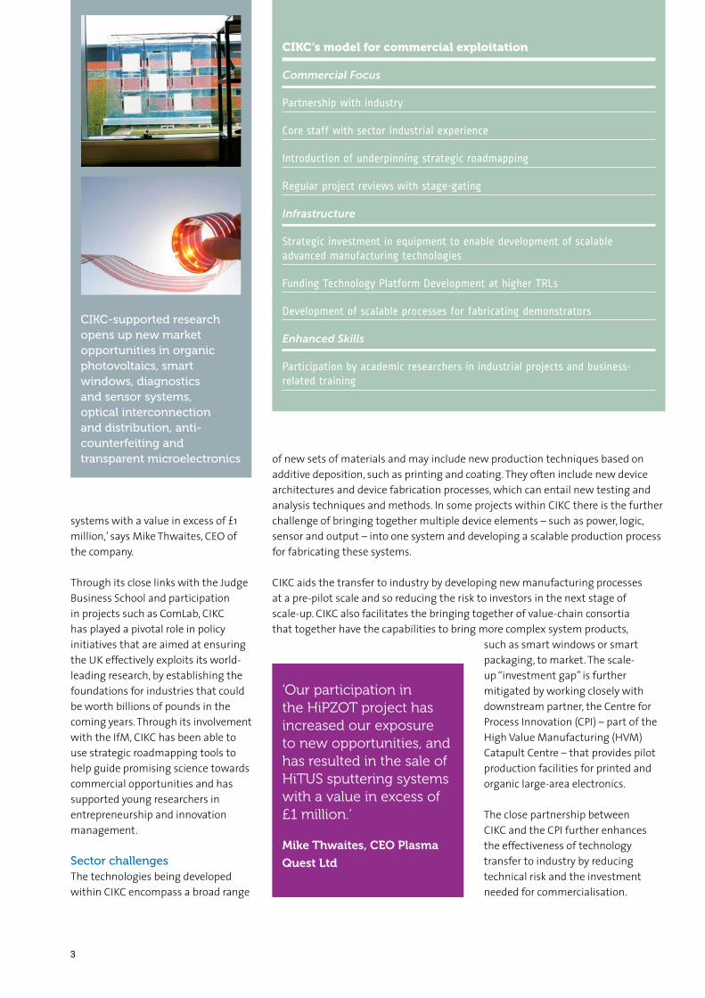
EPSRC Investment – £6.65 million over six years = £1.13 million pa
– 70 FTE years
Outreach
Training
Small Grants
Support Costs
Commercialisation Projects
Equipemnt
Technology Projects
Training£187,360
Technologyprojects£2,664,572
Equipment £1,315,868
Commercialisationresearch
£1,149,130
Supportcosts
£975,428
Small grants£287,860
Outreach£71,672

5
Leveraged funding
Business support 81 companies involved with CIKC projects and follow-on projects
143 companies CIKC has interacted with (meetings, events attended, project participation)
609 person-days use of equipment by industry
Plasma Quest Ltd – £1 million of equipment sales arising from participation in HiPZOT project
Co-locationPragmatIC Printing Limited – 7–10 employees, following small grant/TSB project
3T Technologies – 1 employee and patterning equipment, following small grant project
NanoInk – equipment loan
Dow Corning – 1 employee and 2 years of secondment to CIKC
18 man years of embedded researchers
EPSRC Grant£6,651,890
University of Cambridge income £33,765,663
CIKC £6,651,890
Venture Capitalraised
£4,500,000
Other income£74,668
Industry Income£6,882,262
Other RCs£3,152,000
Other grant income £544,500
EU projects £1,072,501
TSB projects £1,752,417
Other EPSRCgrants
£9,135,424
Total Project size £58,798,273
CIKC £8,022,787
Venture Capitalraised
£4,500,000
Other income £74,668
Industry Income £6,882,262
Other RCs £3,152,000
Other grant income £561,250 EU projects
£16,154,454.40
TSB projects£8,031,571
Other EPSRC grants £11,419,280
2 spinoutsEight19 (2010) from 3PV project
CamLase (2011) from a “Small Grant” project
PLUS 4 others currently under discussion
23 patent applications by end of 2012
84 Papers published
111 Invited talks
81 Students and post-docs contributed to CIKC projects
237 Students attended entrepreneurship courses

6 CIKC Final Report
A characteristic theme running through all CIKC’s technology projects is the use of low-temperature
processes to fabricate electronic and photonic devices. CIKC’s technology scope includes what has now become known as organic and large-area electronics (OLAE) in which low-temperature fabrication processes enable the use of new active materials such as small molecules, polymers and oxides deposited onto flexible substrates such as paper and plastic. Device examples made in this way include transistors, light emitters and detectors, photovoltaics, displays (both emissive and reflective) and sensors. Patterning may be achieved through additive processes, like printing, that can drive lower manufacturing cost. CIKC’s scope also includes the use of organic materials deposited directly onto “active substrates” as in the liquid crystal on silicon (LCoS) process.
CIKC technology portfolio
The initial round of technology projects supported by CIKC funding set up infrastructure for fabricating a range of devices
The initial round of technology projects set up infrastructure for fabricating a variety of devices. This includes a low temperature sputter deposition tool, HiTUS, for reactively sputtering thin films at high rates with exceptional control of material properties. Because the system does not require heating of the substrate it enables the deposition of a wide range of transparent conducting oxides on plastic substrates for flexible electronics.
Other equipment sets include complete bench-top plastic processing techniques for laminating liquid crystal (LC) displays and other devices on plastic, based on hot melt screen printing, roll coating, sheet coating and other processes. CIKC’s equipment portfolio also includes an inkjet printer.
The infrastructure is deployed through Open Access initiatives, a Small Grants programme and through collaborative R&D projects. Researchers can gain access to organic electronics printing facilities within the Cavendish Laboratory. Photolithography and wet benches within a cleanroom facility in the Electrical Engineering Division are also available. Back-end processing on the silicon CMOS platform embraces many aspects of nanotechnology, semiconductor device engineering and optical communications and is a basic resource across much of electronics and photonics. CIKC has also put in place equipment to allow die level assembly of LCoS and related device prototypes.
CIKC’s technology project portfolio comprises six large technology development projects and 16 small grant projects:
High-speed self-aligned printable organic CMOS transistors
Since interest in printed and organic electronics started to build two decades ago, one of the most compelling, albeit challenging, applications has proven to be printable organic transistors. The technology has significant application potential in several markets as it paves the way for simple intelligent devices that can be embedded into clothing, toys, games and everyday items. Smart labels, backplane circuits for next generation flexible displays and transducers for biological or chemical sensors are just some examples of how the technology could be used in the coming years. Once flexible displays, the first generation of polymer electronic products that are now close to industrial production, are validated successfully in the marketplace, the much anticipated market pull for organic transistors in other applications and sectors will intensify.

7
CIKC-FUNDED RESEARCHPrinted polymer transistor technology currently still falls short of the performance requirements of many applications beyond a first generation of applications in flexible, reflective displays. A lot of research in recent years has focussed on improving basic transistor performance through use of novel materials and impressive demonstrations have been made of organic integrated circuits fabricated by conventional lithographic techniques, for example by the Holst Centre in the Netherlands. Professor Henning Sirringhaus, within the Cavendish Laboratory, observes: ‘When incorporating these materials into scalable printing processes, circuit performance is usually found to be much lower. This has prevented the use of organic transistors for applications in smart objects, and companies, such as Plastic Logic, have focused instead on display applications, for which adequate performance has been achievable.’
Sirringhaus’ team developed a scalable, high-performance printing-based manufacturing process for polymer transistor circuits, using an approach for downscaling printed TFTs called self-aligned printing (SAP).
The SAP technology, protected by several patent applications, can
Professor Henning Sirringhaus
A flexible transistor circuit driving an e-paper display
produce high-performance printed thin film transistors (TFTs) operating below 5V. With this technology the group was able to fabricate n-type and p-type self-aligned printed transistors with comparable mobilities, the building blocks for CMOS integrated circuits that are needed for more complex printed logic applications such as radio frequency identification (RFID).
CIKC provided the funding that Sirringhaus and his team needed to take discoveries further and to develop logic capability that industrial partner Plastic Logic is using to develop interactive labels. Recently, the team identified several simple applications in wearable electronics and games and toys that required low cost interactive labels to achieve novel effects.
BENEFIT‘We’ve had more meaningful dialogue and provided Plastic Logic with more relevant technology,’ says Sirringhaus. This has led to a collaborative project, funded by the Technology Strategy Board (TSB), where smart label applications are being developed for commercialisation by CIKC and Plastic Logic with industrial partners. The label components – logic, display and sensors – are made using printable organic inks. The Functional Integrated Plastic Systems (FIPS) project is developing printable electronic labels for brand-enhancement applications, with a
leading fast-moving consumer goods (FMCG) brand owner and the Centre for Process Innovation as well as other partners.
‘CIKC funding has meant that we could establish a team of two to three engineers over a five year duration to develop key manufacturing processes and a practical approach to system integration. This has allowed the group to work on a level that is internationally competitive,’ adds Sirringhaus.
‘CIKC funding has meant that we could establish a team of two to three engineers over a five year duration to develop key manufacturing processes and a practical approach to system integration. This has allowed the group to work on a level that is internationally competitive.’
Professor Henning
Sirringhaus

8 CIKC Final Report
Mike Banach, Research Manager at Plastic Logic, comments: ‘The circuit design and application-specific know-how of Henning’s team created a perfect synergy with our mature transistor technology. Together we can now engage with a new community of end-users for flexible electronics. The collaboration allowed us to tap into expertise that we didn’t have in-house and make progress very quickly.’
Liquid crystal on silicon (LCoS) devices for phase-only holographyHolography based on phase-only liquid crystal on silicon (LCoS) devices opens up a wide range of new display applications, including automotive head-up displays (HUD) and 3D displays.
LCoS technology was initially developed for microdisplays for rear projection video displays, to compete with active matrix liquid crystal displays (AMLCD), and picoprojectors.
Unlike LCD projectors which use transmissive technology, where light is modulated as it passes through the liquid crystal cells, LCoS devices are reflective. In an LCoS device the liquid crystal layer is applied directly to the surface of a silicon CMOS chip and is addressed via arrays of several million pixel electrodes formed in the top layer metallization of the chip, each with its own drive electronics. Typically LCoS devices using amplified modulation are used in video projectors.
Though phase-only LCoS holographic devices are more challenging to manufacture they open up exciting new applications such as the potential for dynamic computer-generated holography. Unlike amplitude modulators, phase-only LCoS holographic devices do not
Professor Daping Chu
absorb or block incident light but instead “redirect” it all into the image. This reduces power consumption and projector size and, more importantly, allows images to be displayed on non-planar surfaces and in 3D.
A hologram may be created in the liquid crystal layer by applying a spatially varying voltage pattern on the pixel electrodes, which when illuminated by laser light, acts to project an image by diffraction. This voltage pattern may be computer-generated in real time and written to the LCoS chip, to produce a video image, creating a high quality display.
CIKC-FUNDED RESEARCHThe Photonics and Sensors Group within the University of Cambridge’s Department of Engineering had established itself as a leader in the development of LCoS technologies and associated manufacturing processes under the leadership of Emeritus Professor Bill Crossland. CIKC funding for the project PASSBACK enabled state-of-the-art facilities for assembling and testing phase-only LCoS devices to be installed at the University. These include equipment for semi-automated cell assembly and for the examination of backplanes and completed LCoS devices.
The funding enables the group to produce high quality LCoS devices at pre-production scale, with repeatability and reliability that is necessary for prototyping commercial products. The main technical challenges to overcome in the assembly process are to ensure that the backplane and the cover-glass are physically parallel and as flat as possible and then to design equipment to perform phase profiling over the chip surface so that any remaining deviations can be compensated for in
Commercial applications for phase-only LCoS holographic devices
Application Market
3D televisions Displays; entertainment, gaming, buildings
Head-up displays Automotive
Biomedical imaging Healthcare and biomedicine and testing
Advanced high precision Industrial tools, such as laser manufacturing maskless lithography
Fibre optic switch Telecoms/internet infrastructure

9
software. Currently, the assembly process achieves better than 50 nm cell gap uniformity over 25 mm die.
BENEFITAs a consequence of the equipment investment made possible by the CIKC funding, the group – now under the leadership of Professor Daping Chu – has developed strong expertise in the custom design of prototype devices and LC materials for phase-only holography, and for telecoms applications as well as displays.
‘This has led to several interesting early-stage commercial developments,’ says Chu. ‘In one instance we supplied LCoS devices for an industry partner’s prototype modules for holographic HUDs for the automotive industry, tested by an automotive OEM.’
As a result, a UK partner, technology start-up Two Trees Photonics based in Milton Keynes, has acquired the rights to use the technology in an HUD application for the automotive market. The group has also fabricated LCoS devices for proof-of-principle prototypes of an advanced optical communications switch and patents have been filed. The unique capabilities of phase-only LCoS to provide software-controllable wavelength separation, beam steering, multicasting and aggregation suggest the technology could play a pivotal role in realising the next generation of optical network components in the
telecommunications industry, such as reconfigurable add/drop multiplexers (ROADMs). Transition to higher data rates, up to 40-Gb/s and ultimately 100-Gb/s, will further propel demand for phase-only LCoS.
Through its continued research programme the group is investigating several other promising applications for phase-only LCoS.
Large-area bistable reflective colour displays on plastic
Reflective displays have attracted more R&D investment and commercial interest in recent years. This is largely due to the success of E Ink, which has enabled the e-reader market with its electrophoretic (‘e-paper’) frontplane laminates.
Like any other e-paper displays Smectic A (SmA) liquid crystal (LC) devices have low power consumption and good readability in bright light. But the technology also has distinct advantages over competing technologies, including high brightness, perfectly clear transparent state and full-colour in a stacked architecture with subtractive colour modulation (like cyan, magenta and yellow inks in printing systems) without the use of filters and increased optical efficiency due to operation on both light polarisations. Simple passive matrix drive is also possible for many applications.
Developing all-plastic SmA e-paper, compatible with high volume large-area roll-to-roll (R2R) techniques, can produce durable rugged low-cost devices for a range of commercial applications that include outdoor signage and advertising, retail electronic shelf displays, passenger/public information screens, as well as smart glass for radiation control in buildings.
CIKC-FUNDED RESEARCHEarlier projects by the Photonics and Sensors Group in the Department of Engineering at the University of
‘In one instance we supplied LCoS devices for an industry partner’s prototype modules for holographic HUDs for the automotive industry, tested by an automotive OEM.’
Professor Daping Chu
A phase-only holographic colour image projection system
Laser light spot diffracted from a test pattern on an LCoS chip
10 CIKC Final Report
Advantages of SmA liquid crystal technology
Bistable; displays have very low power consumption
Multilevel greyscale response has been demonstrated
Good white state
Excellent transmittance in the clear state
Applications and markets
Outdoor advertising and signage
Public information screens
Electronic shelf labels for retail
Smart windows for control of solar gain in buildings
Smart skins and cladding for buildings
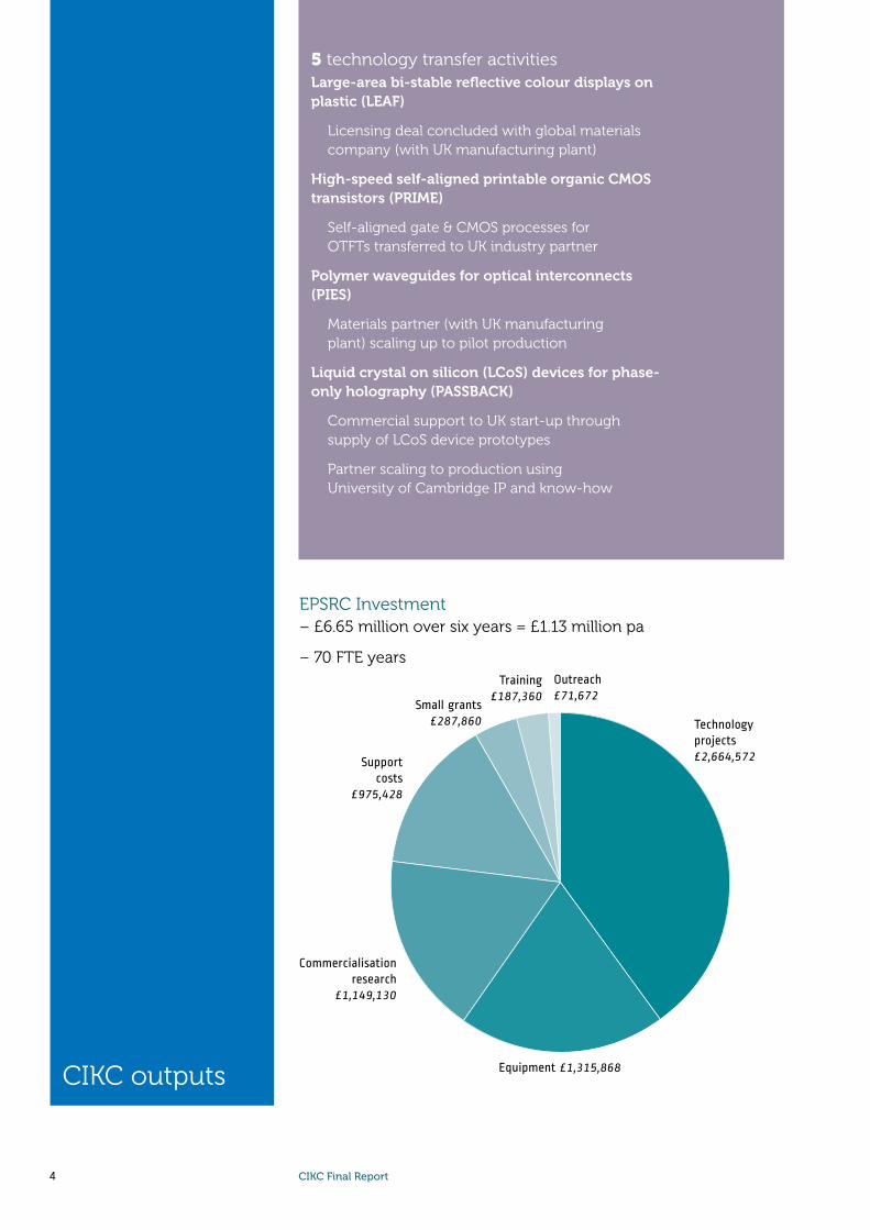
The TSB-funded PICWIN project, which followed on from the CIKC-funded LEAF project, enabled the production of large size demonstrators
Cambridge developed good quality black and white displays on glass using SmA LC materials supplied by industrial partner Dow Corning. With CIKC funding the group, led by Professor Daping Chu, was able to develop a process for producing reflective displays on plastic substrates for the first time by setting up a lamination facility to encapsulate the SmA LC materials between two plastic sheets to produce a laminated electro-active foil (LEAF). The basic lamination technology and processing conditions
‘CIKC’s projects are aligned with Dow Corning’s own R&D activities, and have helped further support our customers’ innovation in areas such as big data computing and sustainable urban development.’
Dr Terry Clapp
were then further optimised. The LEAF project resulted in the demonstration of passive matrix displays with large area single pixels based on SmA LC materials on A5 size plastic substrates by lamination. The project also demonstrated full colour displays, using stacked layers of colour dyed cells in yellow, magenta and cyan. Since SmA LC devices are transparent in one of their optical states much brighter images can be produced. The dyes, made from customised black dye mixtures, can withstand millions of switching operations that are required for commercial applications.
BENEFITDuring the course of the project other potential applications, for the construction industry, were also identified. These include switchable window laminates for solar radiation control to improve energy efficiency in buildings by alleviating air-conditioning use in the summer time.
Chu says: ‘While we began this work initially with display applications in mind, through our roadmapping meetings additional opportunities in the construction industry became clear. Our industrial partner, Dow Corning, is very interested in these as the company is already a supplier to the construction industry. Furthermore, in building applications, the LEAF technology can also be used for retro-fitting existing buildings, a market which is substantially larger than new construction.’
Dow Corning participated in the establishment of the CIKC and seconded an employee, Dr Terry Clapp, as Director for the first two years of the Centre. He says: ‘The Centre’s projects are aligned with Dow Corning’s own R&D activities, and have helped further support our customers’ innovation in areas such as big data computing and sustainable urban development.’
DEMONSTRATORThe Technology Strategy Board (TSB)-funded PICWIN (Picture Window) project enabled the production of large size demonstrators for a controllable optical film for the built environment, able to provide solar radiation control and to provide low

11
resolution digital display of information. Partners included the Centre for Process Innovation (CPI), Timsons Ltd, DuPont Teijin Films and Vector Foiltec, which makes lightweight cladding for buildings using ethylene tetra fluoro ethylene (ETFE) films.
The team is working with several industrial partners and a technology transfer agreement concerning some of the technology developed in the LEAF project has recently been signed between the University of Cambridge and a global company to explore this technology in the smart window market.
Printed organic photovoltaics fabricated using R2R printing processesThe printing and coating of functional inks to manufacture ‘organic photovoltaics’ (OPV) has the potential to reduce the cost of solar electricity generation, opening up many new market opportunities for the technology. IDTechEx estimates that the OPV market today worth is $4.6 million and forecasts that it will rise to $630 million in 2022.
When scaled, fabrication of OPV modules over large area plastic substrates can reduce production costs considerably. However, a key benefit of OPV technologies is their potential for integration with other materials and products, opening up new applications for electricity generation and energy harvesting from a renewable resource. For example OPV films can be laminated, or coated, onto substrates and components as part of steps in production and manufacturing.
CIKC-FUNDED RESEARCHFunding enabled the research team, led by Professor Neil Greenham, to focus on taking previously discovered
materials to develop a process for manufacturing OPV devices using large-area R2R production techniques within the Printed Polymer Photovoltaics (3PV) project.
The project investigated the process steps required to pattern plastic substrates, deposit active semiconductor layers over large areas and interconnect the cells. In establishing the steps and translating cell fabrication to large-area R2R production techniques, while maintaining higher efficiencies achieved in lab results, Greenham’s team generated fundamental process IP that is applicable to a range of materials sets.
3PV resulted in the development of processes for device fabrication that could be scaled for full production, taking into account the anticipated advances in OPV efficiencies and other performance criteria, thereby taking research closer to market.
The funding from CIKC was instrumental in the University of Cambridge’s negotiations with stakeholder Carbon Trust
Professor Neil Greenham
The CIKC-funded project 3PV resulted in the development of processes for OPV device fabrication that could be scaled for full production
3PV PROJECT ACHIEVEMENTS
Demonstration of printing processes for coating the OPV layers
Specification, procurement and commissioning of large-scale print equipment
Demonstration of flexible PV modules with printed active layers
Development of a patented patterning process
Transfer of the technology to a spinout (Eight19)
12 CIKC Final Report
to launch the Advanced Photovoltaic Research Accelerator. The Accelerator resulted in the spin-out of Eight19 in September 2010, with £4.5 million in funding from Carbon Trust and European specialty chemicals company Rhodia.
BENEFITBased in premises on the Cambridge Science Park, Eight19 employs the four University of Cambridge researchers originally working on 3PV, a CEO and additional staff. In January 2012 the company installed a printing facility that includes a multi-station R2R machine able to deposit and pattern liquid active layers for solar modules at a peak linear speed of over 3.6 km an hour.
In addition to developing a production process for printed polymer solar cell technology, early on Eight19 identified a commercial application and product, a portable pay-as-you-go (PAYG) solar-powered lamp and phone charger for off-grid markets where millions are without access to electricity, opening up potential markets for the company’s OPV modules in future. The product, called Indigo, is made from commercially available silicon modules and LEDs.
‘CIKC funding has allowed us to take our OPV research programme a step closer to manufacturing than our normal funding sources would have allowed. Transferring the technology to a company that is focused on taking it to market is exactly what we wanted to achieve.’
Professor Neil Greenham
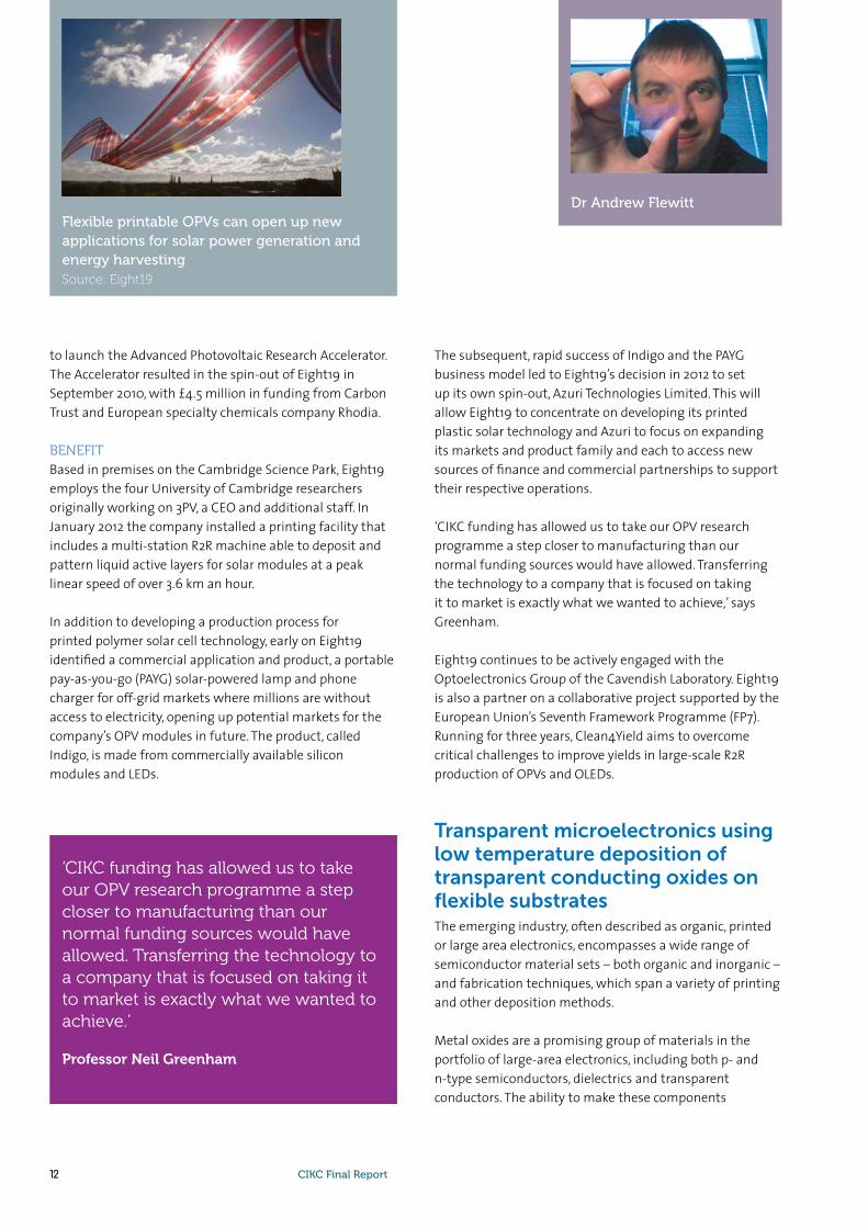
Flexible printable OPVs can open up new applications for solar power generation and energy harvesting Source: Eight19
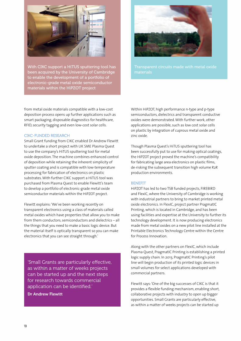
Dr Andrew Flewitt
The subsequent, rapid success of Indigo and the PAYG business model led to Eight19’s decision in 2012 to set up its own spin-out, Azuri Technologies Limited. This will allow Eight19 to concentrate on developing its printed plastic solar technology and Azuri to focus on expanding its markets and product family and each to access new sources of finance and commercial partnerships to support their respective operations.
‘CIKC funding has allowed us to take our OPV research programme a step closer to manufacturing than our normal funding sources would have allowed. Transferring the technology to a company that is focused on taking it to market is exactly what we wanted to achieve,’ says Greenham.
Eight19 continues to be actively engaged with the Optoelectronics Group of the Cavendish Laboratory. Eight19 is also a partner on a collaborative project supported by the European Union’s Seventh Framework Programme (FP7). Running for three years, Clean4Yield aims to overcome critical challenges to improve yields in large-scale R2R production of OPVs and OLEDs.
Transparent microelectronics using low temperature deposition of transparent conducting oxides on flexible substratesThe emerging industry, often described as organic, printed or large area electronics, encompasses a wide range of semiconductor material sets – both organic and inorganic – and fabrication techniques, which span a variety of printing and other deposition methods.
Metal oxides are a promising group of materials in the portfolio of large-area electronics, including both p- and n-type semiconductors, dielectrics and transparent conductors. The ability to make these components
13
from metal oxide materials compatible with a low-cost deposition process opens up further applications such as smart packaging, disposable diagnostics for healthcare, RFID, security tagging and even low-cost solar cells.
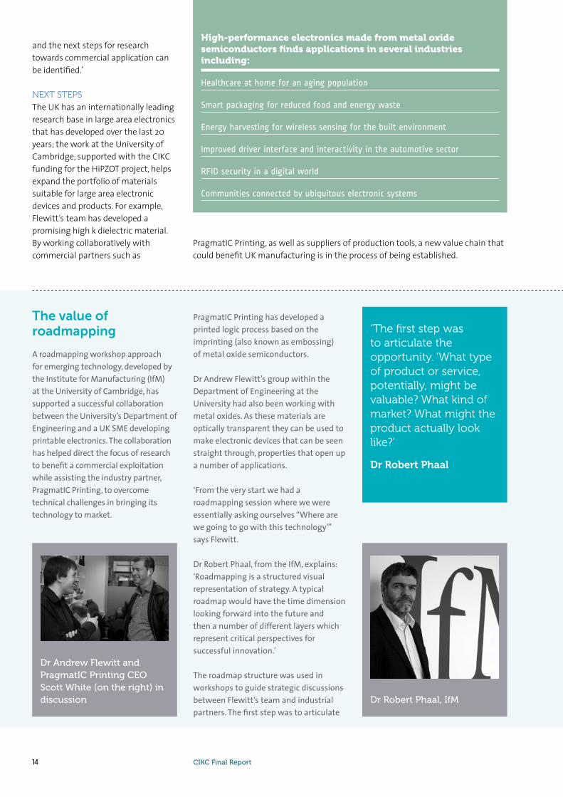
CIKC-FUNDED RESEARCHSmall Grant funding from CIKC enabled Dr Andrew Flewitt to undertake a short project with UK SME Plasma Quest to use the company’s HiTUS sputtering tool for metal oxide deposition. The machine combines enhanced control of deposition while retaining the inherent simplicity of sputter coating and is compatible with low-temperature processing for fabrication of electronics on plastic substrates. With further CIKC support a HiTUS tool was purchased from Plasma Quest to enable Flewitt’s team to develop a portfolio of electronic-grade metal oxide semiconductor materials within the HiPZOT project.
Flewitt explains: ‘We’ve been working recently on transparent electronics using a class of materials called metal oxides which have properties that allow you to make from them conductors, semiconductors and dielectrics – all the things that you need to make a basic logic device. But the material itself is optically transparent so you can make electronics that you can see straight through.’
Within HiPZOT, high performance n-type and p-type semiconductors, dielectrics and transparent conductive oxides were demonstrated. With further work, other applications are possible, such as low cost solar cells on plastic by integration of cuprous metal oxide and zinc oxide.
Though Plasma Quest’s HiTUS sputtering tool has been successfully put to use for making optical coatings, the HiPZOT project proved the machine’s compatibility for fabricating large area electronics on plastic films, de-risking the subsequent transition high volume R2R production environments.
BENEFITHiPZOT has led to two TSB funded projects, FIREBIRD and FlexIC, where the University of Cambridge is working with industrial partners to bring to market printed metal oxide electronics. In FlexIC, project partner PragmatIC Printing, which is located in Cambridge, and has been using facilities and expertise at the University to further its technology development. It is now producing electronics made from metal oxides on a new pilot line installed at the Printable Electronics Technology Centre within the Centre for Process Innovation.
Along with the other partners on FlexIC, which include Plasma Quest, PragmatIC Printing is establishing a printed logic supply chain. In 2013, PragmatIC Printing’s pilot line will begin production of its printed logic devices in small volumes for select applications developed with commercial partners.
Flewitt says: ‘One of the big successes of CIKC is that it provides a flexible funding mechanism, enabling short, collaborative projects with industry to open up bigger opportunities. Small Grants are particularly effective, as within a matter of weeks projects can be started up
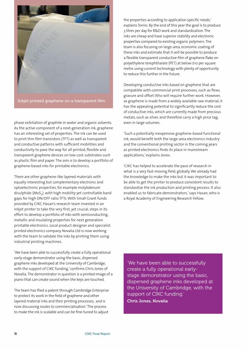
Transparent circuits made with metal oxide materials
With CIKC support a HiTUS sputtering tool has been acquired by the University of Cambridge to enable the development of a portfolio of electronic-grade metal oxide semiconductor materials within the HiPZOT project
‘Small Grants are particularly effective, as within a matter of weeks projects can be started up and the next steps for research towards commercial application can be identified.’
Dr Andrew Flewitt
14 CIKC Final Report
and the next steps for research towards commercial application can be identified.’
NEXT STEPSThe UK has an internationally leading research base in large area electronics that has developed over the last 20 years; the work at the University of Cambridge, supported with the CIKC funding for the HiPZOT project, helps expand the portfolio of materials suitable for large area electronic devices and products. For example, Flewitt’s team has developed a promising high k dielectric material. By working collaboratively with commercial partners such as
The value of roadmapping
A roadmapping workshop approach for emerging technology, developed by the Institute for Manufacturing (IfM) at the University of Cambridge, has supported a successful collaboration between the University’s Department of Engineering and a UK SME developing printable electronics. The collaboration has helped direct the focus of research to benefit a commercial exploitation while assisting the industry partner, PragmatIC Printing, to overcome technical challenges in bringing its technology to market.
PragmatIC Printing has developed a printed logic process based on the imprinting (also known as embossing) of metal oxide semiconductors.
Dr Andrew Flewitt’s group within the Department of Engineering at the University had also been working with metal oxides. As these materials are optically transparent they can be used to make electronic devices that can be seen straight through, properties that open up a number of applications.
‘From the very start we had a roadmapping session where we were essentially asking ourselves “Where are we going to go with this technology”’ says Flewitt.
Dr Robert Phaal, from the IfM, explains: ‘Roadmapping is a structured visual representation of strategy. A typical roadmap would have the time dimension looking forward into the future and then a number of different layers which represent critical perspectives for successful innovation.’
The roadmap structure was used in workshops to guide strategic discussions between Flewitt’s team and industrial partners. The first step was to articulate
Dr Andrew Flewitt and PragmatIC Printing CEO Scott White (on the right) in discussion Dr Robert Phaal, IfM
‘The first step was to articulate the opportunity. ‘What type of product or service, potentially, might be valuable? What kind of market? What might the product actually look like?’
Dr Robert Phaal
High-performance electronics made from metal oxide semiconductors finds applications in several industries including:
Healthcare at home for an aging population
Smart packaging for reduced food and energy waste
Energy harvesting for wireless sensing for the built environment
Improved driver interface and interactivity in the automotive sector
RFID security in a digital world
Communities connected by ubiquitous electronic systems
PragmatIC Printing, as well as suppliers of production tools, a new value chain that could benefit UK manufacturing is in the process of being established.

15
Polymer waveguides for optical interconnects
In-system bandwidth densities driven by interconnect speeds and scalable input/output (I/O) within data storage and server enclosures will continue to increase over the coming years, thereby severely impacting cost and performance in future data centre systems. This is fuelling the migration of optical connectivity into the system enclosure itself and will need to be addressed by disruptive new embedded optical interconnect technologies.
Electro-optical printed circuit boards based on polymer waveguides and supporting technologies can provide the cost viable embedded optical interconnect ‘eco-system’ to mitigate this impending bottleneck. In addition the technology could have a wide range of other potential applications in several large markets such as vehicle wiring looms and data distribution for displays and consumer goods.
‘Our industrial partner Dow Corning believed that its siloxane materials could be used to make polymer waveguides but wanted the materials to be proven in this application,’ explains Professor Richard Penty in the Centre for Photonic Systems in the Department of Engineering.
Siloxane polymers exhibit stable optical performance with very low loss maintained over long lifetimes and
at high temperatures. The materials can be formed into waveguides using simple photolithography/wet chemical and embossing processes and potentially with printing. The polymer material can be processed at low temperature, in contrast to the more conventional high temperature processing required for the formation of glass waveguides. Unlike other polymers, the siloxane system is compatible with high temperature lead-free soldering processes so it can be used in standard printed circuit board processes.
CIKC-FUNDED RESEARCHFunding enabled Penty and his team to demonstrate high quality basic building blocks, including waveguides, bends, couplers and crossings, with excellent performance.
The team was then able to build the first Terabit/s capacity passive router, with 100 waveguides, with up to 90 crossings (which remains world leading in terms of passive router functionality).
An optical waveguide layer on one side of a standard circuit board and electronic components on the other was combined by developing a simple ‘L connector’ where surface-emitting lasers and photodiodes are slotted through the circuit board and connected to both the electronic components and the waveguides. This enabled the demonstration of a 10Gb/s ONU transceiver circuit with error free operation in Tx and Rx modes and the realisation
The second part of the workshop – the core of the exercise – was identifying a set of logical steps towards that value. This enables a group working on a new technology to identify the key opportunities that they see in the future and the routes to capture that value.
It became clear that PragmatIC’s focus aligned with the area of logic on plastic that Flewitt’s team identified in the roadmapping. This led to an initial Small Grant project, IZONANO, looking at the specific metal oxides that the Cambridge team had been working on and applying these to PragmatIC’s device architectures.
The collaboration intensified with employees of PragmatIC working side by side with the post-docs and PhD students in Flewitt’s research group.
‘My message from PragmatIC to other SMEs looking at collaborating with the Engineering Department at Cambridge would be that it is well worth the effort. This is something that can be highly beneficial both from a financial perspective and in terms of getting access to expertise that really is world-class,’ says White.
Electronics on a bottle label
‘It’s not just every six months that PragmatIC gets some dry report from us, it is a day-by-day evolving collaboration.’ Dr Andrew Flewitt
the opportunity. ‘What type of product or service, potentially, might be valuable? What kind of market? What might the product actually look like?’ says Phaal.

16 CIKC Final Report
of an on-board 4x10Gb/s parallel interconnect.
A multi-channel scalable waveguide layout comprising a wide range of passive multimode components was then designed and implemented with Dow Corning’s materials on low-cost FR4 substrates. As a proof-of-principle, 4-channel 3-card optical bus modules have been fabricated and interconnected via a prototype 4 x 10 Gb/s opto-electronic 3R (reamplifying, reshaping and retiming) regenerator.
Professor Richard Penty
The 4x10Gb/s optical bus demonstrator shows how light is guided using polymer waveguides, opening up potential application for board-level optical interconnects
‘We see the optical waveguide PCB activities being carried out at the CIKC as a very strong contender to satisfy the requirements of next generation system embedded optical interconnect solutions, given the disruptive optical design activities, successful deployment into hybrid electro-optical PCB and the quality of the Dow Corning optical polymer itself.’
Richard Pitwon, Xyratex
The final step of the project integrated polymer waveguides, electronics and optoelectronics onto a standard circuit board using a low cost interconnect technology with integrated transceivers operating at data rates up to 10Gb/s.
BENEFITThe main outcome of the work, to date, has been the development of a low-cost manufacturing approach using materials compatible with the high temperature steps in conventional circuit board manufacture and a novel solution for high performance computer interconnect interfacing issues, which has also led to new photonic systems concepts. The next step is to take the technology to the stage where it can be readily transferred to production.
‘We see the optical waveguide PCB activities being carried out at the CIKC as a very strong contender to satisfy the requirements of next generation system embedded optical interconnect solutions, given the disruptive optical design activities, successful deployment into hybrid electro-optical PCB and the quality of the Dow Corning optical polymer itself,’ says Richard Pitwon, lead photonics engineer at Xyratex, a global supplier of data storage technologies with facilities in Havant, Southampton.
Xyratex is leading a collaborative project bid for EU funding to develop such an embedded optical ‘eco-system’, which includes companies in the PCB, transceiver and connector industry.
Small Grant projects
CIKC has operated a mechanism for providing seed funding, known as a “Small Grant” to researchers wishing to test the feasibility of brand new concepts within CIKC’s scope of operation. It is intended that the small projects should be designed so that, if successful, they produce results which can be used as the basis for much larger projects. Small Grant funding has been used to test the feasibility of a blue-sky idea, a new manufacturing process and built first demonstrators of new application ideas. Here are two examples:
Portable laser demonstrator for printable liquid crystal laser materials
Tuneable laser systems, such as Ti:sapphire and dye lasers, are large, fixed, complex and expensive. A research team at the University of Cambridge had developed a method to print lasers made from LC materials using inkjet printing equipment.

17
Typically lasers are made from materials which require expensive manufacturing processes and only work on certain surfaces.
The printable laser materials are made from cholesteric LCs, which are aligned by the application of standard polyvinyl acetate (PVA) polymer on a substrate, such as glass, using a simple bar-coating method. The laser deposits, each less than 500 microns in width, are then printed onto the polymer. The colour of the laser emission is controlled by a chiral additive and fluorescent dye. The printed LC lasers can emit light anywhere in the 400 to 850 nm range. The research team at the Centre of Molecular Materials for Photonics and Electronics (CMMPE), working under the EPSRC
‘Having a portable prototype is really important as it means we can show a working demonstrator to potential investors, customers and development partners, so they can see how simply it can be utilised or deployed.’
Dr Damian Gardiner
funded COSMOS project, collaborated with the Inkjet Centre at the IfM, both in the Department of Engineering at the University of Cambridge.
The discovery could lead to a low-cost and compact alternative to existing tuneable laser technology enabling a host of new applications for lasers, such as functionalising large area surfaces to create displays on walls. The technology also promises a low-cost method for making bioassay arrays for detecting viruses and pathogens, which could benefit healthcare and other sectors. Brand protection and security printing could also benefit from the technology as the lasers can be deposited on a range of coated substrates, including plastic film and even paper.
In order to demonstrate the potential of this promising technology for the security industry, the research team used a small grant from the CIKC to build a compact, A4 footprint, portable demonstrator to probe printed laser films.
Dr Damian Gardiner, who worked on the project, explains: ‘CIKC funding in the Portable Printable Laser Demonstrator (PORTALS) project has been used to bridge the gap between fundamental research and making a prototype detector to “read” the light emission from the printed LC lasers and confirm laser operation. Having a portable prototype is really important as it means we can show a working demonstrator to potential investors, customers and development partners, so they can see how simply it can be utilised or deployed.’
After completion of the project, Gardiner and his colleagues worked with the University’s organisation i-Teams, which takes PhD students and post-docs and exposes them to a new technology or invention and examines potential applications. He also engaged with Cambridge Enterprise, the University’s technology transfer arm, to formulate commercial exploitation opportunities and ideas. Gardiner recently secured a Royal Academy of Engineering Enterprise Fellowship to pursue commercialisation routes currently under discussion.
Inkjet printing of graphene and 2D materials: a new platform for cheap, flexible and transparent electronics
Researchers at the University of Cambridge have developed solution processable graphene functional inks for printed and large area electronics applications.
The team, which includes Dr Tawfique Hasan, Felice Torrisi and Prof Andrea Ferrari of Cambridge Graphene Centre recently produced a graphene-based ink by liquid
Dr Damian Gardiner Exciting laser action in a coated liquid crystal film on paper
18 CIKC Final Report
phase exfoliation of graphite in water and organic solvents. As the active component of a next-generation ink, graphene has an interesting set of properties. The ink can be used to print thin film transistors (TFT) as well as transparent and conductive patterns with sufficient mobilities and conductivity to pave the way for all-printed, flexible and transparent graphene devices on low-cost substrates such as plastic film and paper. The aim is to develop a portfolio of graphene-based inks for printable electronics.
There are other graphene-like layered materials with equally interesting but complementary electronic and optoelectronic properties, for example molybdenum disulphide (MoS2), with high mobility yet controllable band gaps for high ON/OFF ratio TFTs. With Small Grant funds provided by CIKC Hasan’s research team invested in an inkjet printer to take the very first, yet crucial, steps in its effort to develop a portfolio of inks with semiconducting, metallic and insulating properties for next generation printable electronics. Local product designer and specialist printed electronics company Novalia Ltd is now working with the team to validate the inks by printing them using industrial printing machines.
‘We have been able to successfully create a fully operational early-stage demonstrator using the basic, dispersed graphene inks developed at the University of Cambridge, with the support of CIKC funding,’ confirms Chris Jones of Novalia. The demonstrator in question is a printed image of a piano that can create sound when the keys are touched.
The team has filed a patent through Cambridge Enterprise to protect its work in the field of graphene and other layered material inks and their printing processes, and is now discussing routes to commercialisation. ‘The process to make the ink is scalable and can be fine-tuned to adjust
Inkjet printed graphene on a transparent film
the properties according to application specific needs,’ explains Torrisi. By the end of this year the goal is to produce 3 litres per day for R&D work and standardization. The inks are cheap and have superior stability and electronic properties compared to existing organic polymers. The team is also focusing on large-area, economic coating of these inks and estimate that it will be possible to produce a flexible transparent conductive film of graphene flake on polyethylene terephthalate (PET) at below £10 per square metre using current technology with plenty of opportunity to reduce this further in the future.
Developing conductive inks based on graphene that are compatible with commercial print processes, such as flexo, gravure and offset litho will require further work. However, as graphene is made from a widely available raw material, it has the appealing potential to significantly reduce the cost of conductive inks, which are currently made from precious metals, such as silver, and therefore carry a high price tag, even in large volumes.
‘Such a potentially inexpensive graphene-based functional ink, would benefit both the large-area electronics industry and the conventional printing sector in the coming years as printed electronics finds its place in mainstream applications,’ explains Jones.
‘CIKC has helped to accelerate the pace of research in what is a very fast-moving field, globally. We already had the knowledge to make the inks but it was important to be able to get the printer to produce consistent results to standardize the ink production and printing process. It also enabled us to fabricate demonstrators,’ says Hasan, who is a Royal Academy of Engineering Research Fellow.
‘We have been able to successfully create a fully operational early-stage demonstrator using the basic, dispersed graphene inks developed at the University of Cambridge, with the support of CIKC funding.’Chris Jones, Novalia

19
ComLabThe Commercialisation Laboratory (ComLab) project undertaken by the CBR at the University of Cambridge provided the researchers with the opportunity to observe over a four-year period, how the different technology projects evolved. Traditionally, collaborative research projects tend to focus on addressing a specific problem or challenge. CIKC enables projects that are more focused on commercialisation because of the ability of the centre to switch resources more quickly. This facilitates a dynamic environment in which to accelerate commercially promising research. The differences between the individual CIKC projects, in terms of focus, scope, size and brevity, provided the ComLab team with invaluable insight into resources, barriers and constraints, opportunities, behaviours and expectations that occur along the path towards commercialisation.
Research on innovation processes at the CIKC has had a significant impact on the evolution of innovation policy in the UK, influencing a major new policy initiative of creating institutions that bridge the gap that exists between public sector funding of research and private sector funding of the further development and commercialisation activities that are needed to bring promising technology to market.
The ComLab researchers investigated international models for comparison, including Industrial Technology Research Institute (ITRI), in Taiwan, Holst Centre in the Netherlands and several of the institutes within Germany’s Fraunhofer network. The comparative policy work, based on site visits to these institutes and their equivalents in Japan, South Korea, Belgium and the USA, led to a paper titled ‘Models of Technology Development in Intermediate Research Organisations’, authored by Dr Andrea Mina, Mr David Connell and ComLab leader Professor Alan Hughes.
The paper identified and discussed the characteristics, operating mechanisms and strategic positions of important innovation intermediaries working at the public-private interface. The project’s findings fed directly into ‘The Current and Future Role of Technology
IntroductionThe CIKC commercialisation programme comprised six research projects and involved researchers from the Judge Business School, the Institute for Manufacturing (IfM) and the Centre for Business Research (CBR) working closely with the technology projects. It had four key objectives:
❖ to improve the speed and effectiveness with which CIKC projects move to commercialisation and facilitate access to commercial and funding partners.
❖ to deliver practical, evidence-based policy recommendations to Government, EPSRC, and the University, on how the UK science base can best be exploited for the benefit of the UK economy.
❖ to develop a set of best practice outcome and impact metrics to enable CIKC to be a leader in this area.
❖ to make a significant contribution to the academic literature on technology commercialisation.
Professor Alan Hughes
Commercialisation research
Strategic roadmapping workshop

20 CIKC Final Report
and Innovation Centres in the UK’, a report produced by UK entrepreneur Hermann Hauser presented to Lord Mandelson on April 25, 2010. The CBR team also submitted evidence to the HM Treasury and BIS consultation document ‘Financing a Private Sector Recovery’ in December 2010.
CatapultsBased on the recommendations of the Hauser Report, the UK Technology Strategy Board (TSB), sponsored by the Department for Business Innovation and Skills (BIS), has established a network of seven technology and innovation centres – Catapults – all of which will be open for business in 2013 and will be supported with an investment of around £1 billion in the coming few years. The centres are:
❖ Cell therapy ❖ Connected digital economy ❖ Future cities
❖ High-value manufacturing ❖ Offshore renewable energy ❖ Satellite applications ❖ Transport systems
The potential global market that could be accessed by UK businesses through each of the Catapult centres is likely to be worth billions of pounds annually.
The CIKC-funded HiPZOT project, which has supported the development of a promising class of materials for making transparent electronics, has enabled UK SME PragmatIC Printing to advance its technology to the point where the company is leasing a pilot line at the Centre for Process Innovation (CPI) – a partner in the High Value Manufacturing Catapult – to produce printed logic devices in small volumes with commercial partners.
The project portfolio included:
Capability development for Open Innovation (COIN) Letizia Mortara, Tim Minshall (IfM)
Developing an approach for assessing the operational capabilities/skills required to implement successfully an open innovation strategy within an industry underpinned by new technologies
A Dynamic Evaluation of Value Chain Architecture Rowena Wang, Matthias Holweg (JBS)
Developing an understanding of how value chains evolve in emerging technologies
Funding models for technology breakthrough Samantha Sharpe, David Connell, Andy Cosh (CBR) businesses (FTB)
Designing funding pathways for commercial success in early stage technologies
IKCCL Alvaro Figueredo, Arnoud De Meyer (JBS)
Participant observation of the commercialisation process embedded within CIKC technology projects
Commercialisation Laboratory (ComLab) Andrea Mina, David Connell, Alan Hughes (CBR)
International comparison of policy frameworks
Best practice metrics for knowledge exchange
Investigation of innovation dynamics and facilitation of the commercialisation process in CIKC technology projects
Managing International Networks for Jag Srai, Tomas Harrington, Mike Gregory (IfM) Emerging Technologies (MIN)
The design, formation and configuration of industrial networks which can provide routes to capture value from innovative technologies
21
T raining has been a significant part of CIKC’s activities, providing technical and business skills for postdoc researchers.
During the course of the CIKC, training programmes included a six day intensive course, Ignite, delivered by the Centre for Entrepreneurial Learning (CfEL); an evening lecture
Training
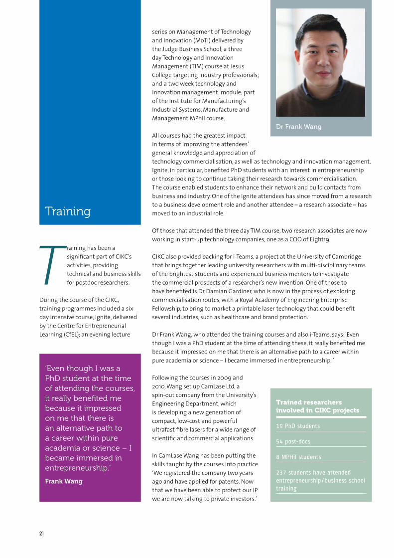
Dr Frank Wang
‘Even though I was a PhD student at the time of attending the courses, it really benefited me because it impressed on me that there is an alternative path to a career within pure academia or science – I became immersed in entrepreneurship.’
Frank Wang
series on Management of Technology and Innovation (MoTI) delivered by the Judge Business School; a three day Technology and Innovation Management (TIM) course at Jesus College targeting industry professionals; and a two week technology and innovation management module; part of the Institute for Manufacturing’s Industrial Systems, Manufacture and Management MPhil course.
All courses had the greatest impact in terms of improving the attendees’ general knowledge and appreciation of technology commercialisation, as well as technology and innovation management. Ignite, in particular, benefited PhD students with an interest in entrepreneurship or those looking to continue taking their research towards commercialisation. The course enabled students to enhance their network and build contacts from business and industry. One of the Ignite attendees has since moved from a research to a business development role and another attendee – a research associate – has moved to an industrial role.
Of those that attended the three day TIM course, two research associates are now working in start-up technology companies, one as a COO of Eight19.
CIKC also provided backing for i-Teams, a project at the University of Cambridge that brings together leading university researchers with multi-disciplinary teams of the brightest students and experienced business mentors to investigate the commercial prospects of a researcher’s new invention. One of those to have benefited is Dr Damian Gardiner, who is now in the process of exploring commercialisation routes, with a Royal Academy of Engineering Enterprise Fellowship, to bring to market a printable laser technology that could benefit several industries, such as healthcare and brand protection.
Dr Frank Wang, who attended the training courses and also i-Teams, says: ‘Even though I was a PhD student at the time of attending these, it really benefited me because it impressed on me that there is an alternative path to a career within pure academia or science – I became immersed in entrepreneurship. ’
Following the courses in 2009 and 2010, Wang set up CamLase Ltd, a spin-out company from the University’s Engineering Department, which is developing a new generation of compact, low-cost and powerful ultrafast fibre lasers for a wide range of scientific and commercial applications.
In CamLase Wang has been putting the skills taught by the courses into practice. ‘We registered the company two years ago and have applied for patents. Now that we have been able to protect our IP we are now talking to private investors.’
Trained researchers involved in CIKC projects
19 PhD students
54 post-docs
8 MPHil students
237 students have attended entrepreneurship/business school training
22 CIKC Final Report
CIKC seminars and other eventsTo raise awareness of the projects supported with CIKC funding and their potential commercial relevance, the Centre has organised a series of events, held in Cambridge. The most recent, titled Large Area Electronics: addressing the applications challenge, was held in December 2012, where CIKC hosted a showcase of recent progress towards the commercial application of large-area electronics. At this one-day seminar, leading speakers from industry and academia described the challenges and opportunities for new low temperature manufacturing techniques in photonics and electronics as these are translated from the laboratory to the marketplace.
Lead researchers on each of the CIKC projects, including the small grant funded projects, gave
Outreach
presentations. Plastic Logic, PragmatIC Printing and Novalia, all local SMEs bringing printed electronics technology to market by very different approaches also gave presentations and discussed their collaborations with the University of Cambridge which have been made possible with CIKC funding. The Centre for Process Innovation (CPI) also presented. The CPI is part of the UK’s High Value Manufacturing Catapult Centre and plays a critical role in the manufacturing scale-up of some of the CIKC-supported breakthroughs.
This presentation line-up was important for showing how promising but high-risk R&D, in the field of printable large area electronics is progressing towards the marketplace.
The event was very successful with 130 delegates attending from 50 different companies and universities. Trade and specialist press covered the event in magazines and online, while the presentations from the day were made available to view on the CIKC website to support dissemination.
In addition to organising its own events the CIKC has also participated in international shows and conferences, including Printed Electronics Europe, as well as UK forums such as Innovate etc. CIKC investigators have presented 108 invited talks at conferences and produced 84 peer reviewed papers.
NetworksCIKC has also formed close relationships with other academic institutions and industry partners though a range of local, national and international networks:

23
COLAEIn 2011 many of Europe’s leading R&D organisations active in the sector united to form Commercialisation of Organic and Large Area Electronics (COLAE), a network project funded under the EU-supported Seventh Framework Programme (FP7) that is designed to simplify and accelerate the commercialisation and adoption of organic electronics technology through the creation of industry clusters.
COLAE aims to raise awareness of the diverse range of applications that can potentially use OLAE technology and to reduce the delivery time to market of these products. One of the key aspects that make OLAE technologies so exciting and important – their multiplicity of applications spanning many sectors – is also what has made this collective of technologies so challenging to convert into industrial supply chains and penetrate the market. COLAE aims to demonstrate the major business opportunities that can be explored and exploited, especially for SMEs across Europe.
As the organic and large area electronics market continues to grow and evolve at speed through the promise of new products, developed with lower cost, low energy processes using environmentally friendly materials, COLAE will provide European organisations access to an unparalleled knowledge base and the know-how to implement OLAE technology. It is doing this by harnessing the resources and expertise of its project partners and making these available to both the existing OLAE industry and new organisations entering the market.
Representing the UK in COLAE are the CIKC and the National Centre for Printable Electronics at CPI. CIKC is leading COLAE’s training work package aimed at end users, designers, scientists and engineers to help them understand and appreciate OLAE technology, its capabilities and commercial value across a diverse range of markets. The training programme combines expert technical support with entrepreneurial guidance.
CIKC investigators have presented 111 invited talks at conferences and produced 84 peer reviewed papers.
CIKC has hosted its own events in Cambridge to raise awareness among academia and industry of the projects it has supported and their commercial relevance
PECoEThe Printed Electronics Centre of Excellence (PECoE) network is comprised of the Centre for Plastic Electronics (CPE) at Imperial College London, the Organic Materials Innovation Centre (OMIC) at Manchester University, the Welsh Centre for Printing and Coating (WCPC) at Swansea University, the Cambridge Integrated Knowledge Centre (CIKC) at the University of Cambridge and the CPI Printable Electronics Centre.
The five centres have a Memorandum of Understanding to provide a focused cluster for technology development and prototyping, aiming to translate UK strengths into the industries of the future. This combination of Centres of Excellence provides the UK with a world-class infrastructure that will play a vital role in securing the UK’s position in the global industry in the future.
Cambridge LAE clusterCIKC facilitates the Cambridge LAE cluster group involving 13 companies from the Cambridge region who are involved in research, development or production of large area electronics. The network now meets every quarter to discuss current progress and future opportunities for large area electronics.
COLAECommercialising Organic and Large Area Electronics

24 CIKC Final Report
CIKC Future
C IKC will continue to facilitate the commercial exploitation of the investments it has already made in its major technology portfolio and of new research arising in its technology field, through:
CIKC is open for business
❖ formation of consortia and development of proposals for publicly-funded projects
❖ encouraging the launch of new start-ups where appropriate
❖ continuing to act as a front-door to the wider University and especially to companies within its technology field
❖ promoting networking between University groups and local companies active in the sector
❖ promoting the development of the whole UK sector through participation in the BIS sponsored plastic electronics leadership group
As part of the EU COLAE network CIKC will continue to support the commercialisation of organic electronics technology through provision of appropriate technical and entrepreneurial training.
The CIKC will be strongly involved with the new EPSRC Centre for Innovative Manufacturing in Large-Area Electronics together with the three other partner Universities through the leadership of CIKC Director Chris Rider who is also the Principal Investigator and Director of the new Centre.
For more information contact:Mark LeadbeaterCIKC Programme ManagerElectrical Engineering DivisionUniversity of Cambridge9 JJ Thomson AvenueCambridgeCB3 0FATelephone +44 (0)1223 748370Fax: +44 (0)1223 748342email: [email protected] : www.cikc.org.uk
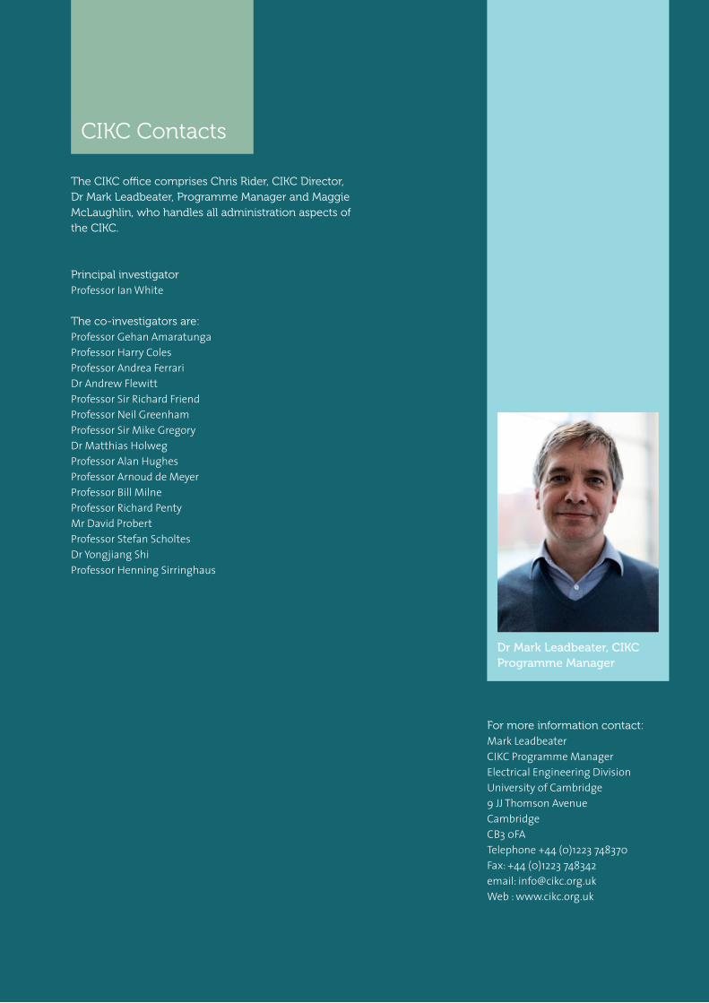
The CIKC office comprises Chris Rider, CIKC Director, Dr Mark Leadbeater, Programme Manager and Maggie McLaughlin, who handles all administration aspects of the CIKC.
Principal investigatorProfessor Ian White
The co-investigators are:Professor Gehan AmaratungaProfessor Harry ColesProfessor Andrea FerrariDr Andrew FlewittProfessor Sir Richard FriendProfessor Neil GreenhamProfessor Sir Mike GregoryDr Matthias HolwegProfessor Alan HughesProfessor Arnoud de MeyerProfessor Bill MilneProfessor Richard PentyMr David ProbertProfessor Stefan ScholtesDr Yongjiang ShiProfessor Henning Sirringhaus
CIKC Contacts
Dr Mark Leadbeater, CIKC Programme Manager

Final Report