Embed Size (px)
Citation preview
ORIGINAL ARTICLE
Broadband optical absorption measurement of silicon nanowiresfor photovoltaic solar cell applications
Md Ali Asgar • Mehedhi Hasan • Md Fazlul Huq •
Zahid Hasan Mahmood
Received: 9 March 2013 / Accepted: 4 December 2013 / Published online: 28 March 2014
� The Author(s) 2014. This article is published with open access at Springerlink.com
Abstract The broadband optical absorption properties of
silicon nanowire films fabricated by electroless metal
deposition technique followed by HF/Fe(NO3)3 solution-
based chemical etching at room temperature on p-type
silicon substrates have been measured and found absorp-
tion higher than that of the solid thin films of equivalent
thickness. The observed behavior is effectively explained
by light scattering and light trapping though some of the
observed absorption is due to a high density of surface
states in the nanowires films. Synthesized structures
absorbed more than 82 % of incident radiation in case of
Cu-deposited silicon nanowires, whereas for Ag it was
maximum 83 %, which is much greater than that of the
bulk silicon as they absorbed maximum 43 % of the
radiation.
Keywords Silicon nanowires (SiNWs) � Electroless
metal deposition (EMD) � Photovoltaic (PV) � Optical
absorption
Abbreviations
SiNW Silicon nanowire
EMD Electroless metal deposition
PV Photovoltaic
HF Hydrogen fluride
SEM Scanning electron micrograph
UV Ultra violet
Introduction
To date, the catastrophic environmental pollution arising
from burning fossil fuels has discriminating public con-
cern, and thus the increasing dependence on renewable
clean energy alternatively. Amongst the alternative energy
sources, solar energy represents one of the most sustain-
able, environmentally acceptable and technologically
promising renewable clean energy sources [1, 2]. Since the
invention of solar cells in the 1950s [3], the solid-state
junction photovoltaic solar cell devices have dominated
photovoltaic solar energy converters. The most common
material used in solar cells is silicon. Silicon accounts for
more than 98 % of the solar cell market [4]. This is pri-
marily because of silicon is earth abundant, highly effi-
cient, and air stable. Crystalline silicon solar cells have
achieved efficiencies approaching 25 % in the laboratory
and 20 % commercially [5]. Much attention has been
drawn on the investigation of solar cells for decades.
A potential candidate for the next generation of solar
cells is silicon nanowires (SiNWs) and have already found
application as antireflective layers [6] and as active
M. A. Asgar
Department of Electronics and Communication Engineering,
Jatiya Kabi Kazi Nazrul Islam University, Trishal, Mymensingh,
Bangladesh
M. Hasan
Department of Electrical and Electronic Engineering, Shahjalal
University of Science and Technology, Kumargaon, Sylhet 3114,
Bangladesh
M. F. Huq (&)
Department of Nuclear Engineering, University of Dhaka,
Dhaka 1000, Bangladesh
e-mail: [email protected]
Z. H. Mahmood
Department of Applied Physics Electronics and Communication
Engineering, University of Dhaka, Dhaka 1000, Bangladesh
123
Int Nano Lett (2014) 4:101
DOI 10.1007/s40089-014-0101-z
elements in organic [7], dye-sensitized [8], quantum-dot
sensitized [9], liquid-junction [10, 11], and inorganic solid-
state devices [6]. SiNWs are 1D material and there has
been interest to incorporate them into photovoltaic cell
design due to the wide availability of the material and
existing processing infrastructure and direct path for charge
transport afforded by the geometry. In addition to that
SiNWs have higher absorption capability, nearly 70 %,
which is much greater than that of bulk silicon [12, 13].
SiNWs show higher absorption since when the SiNW
arrays are placed in orthogonal direction to light absorption
and charge separation by fabricating radial p–n junctions, it
enables efficient carrier collection and light trapping in
optically thick nanowire arrays, even when minority carrier
diffusion lengths are shorter than the optical absorption
length [14–16]. SiNWs arrays also show comparatively
low reflection losses than planner semiconductor [14]
which definitely leads to higher absorption also. The
advantage of using nanowires is that, like quantum dots we
can tune the band gap to a specific part of the solar spec-
trum by simply controlling the chemical composition and
the coverage density of the wire surface. Significant
shrinking of band gap occurs if halogens such as Cl, Br,
and I are used instead of H as surface passivation elements
without changing the characteristics of semiconductor
nanowires [17, 18]. In this paper, we have measured the
optical absorption of SiNWs of different dimensions syn-
thesized by electroless metal deposition (EMD) over the
range or 200–1,000 nm. Our finding shows that the
absorption of SiNWs has greatly modified than that of the
bulk silicon.
Methods
SiNWs array was grown by an aqueous electroless etching
method by depositing noble metal nanoparticle like silver
and copper. The fabrication process of SiNWs composed of
three steps: (1) cleaning of the silicon wafers with ultra-
sonic bath, (2) electroplating the films of metal nanopar-
ticles onto the cleaned silicon surface, and (3) immersion
of the nanoparticle-deposited silicon wafers into HF-based
aqueous chemical etching solutions. All the processes were
conducted in Teflon lined autoclave.
For silver nanoparticle deposition, the concentration of
AgNO3 was 0.02 M with deposition time varied from 60 to
75 s. In case of copper nanoparticle deposition, concen-
tration of Cu(NO3)2 was 0.02 and 0.05 M with deposition
time varied from 60 to 120 s. In both the cases, concen-
tration of HF was 5.0 M. After the electroless deposition of
the silver and copper nanoparticle, the silver/copper metal
covered Si substrate which was confirmed by scanning
electron microscopy (SEM). Then, those metal (Ag/Cu)
deposited Si samples were immersed in an aqueous HF/
Fe(NO3)3 solution for etching. The concentration of HF
and Fe(NO3)3 was 5 and 0.02 M, respectively. Etching was
performed at room temperature for 30–75 min in case of
Ag-treated Si samples and 60–120 min for Cu-deposited Si
samples. Then after the preparation process, the obtained
samples were rinsed copiously in deionized water and dried
at room temperature.
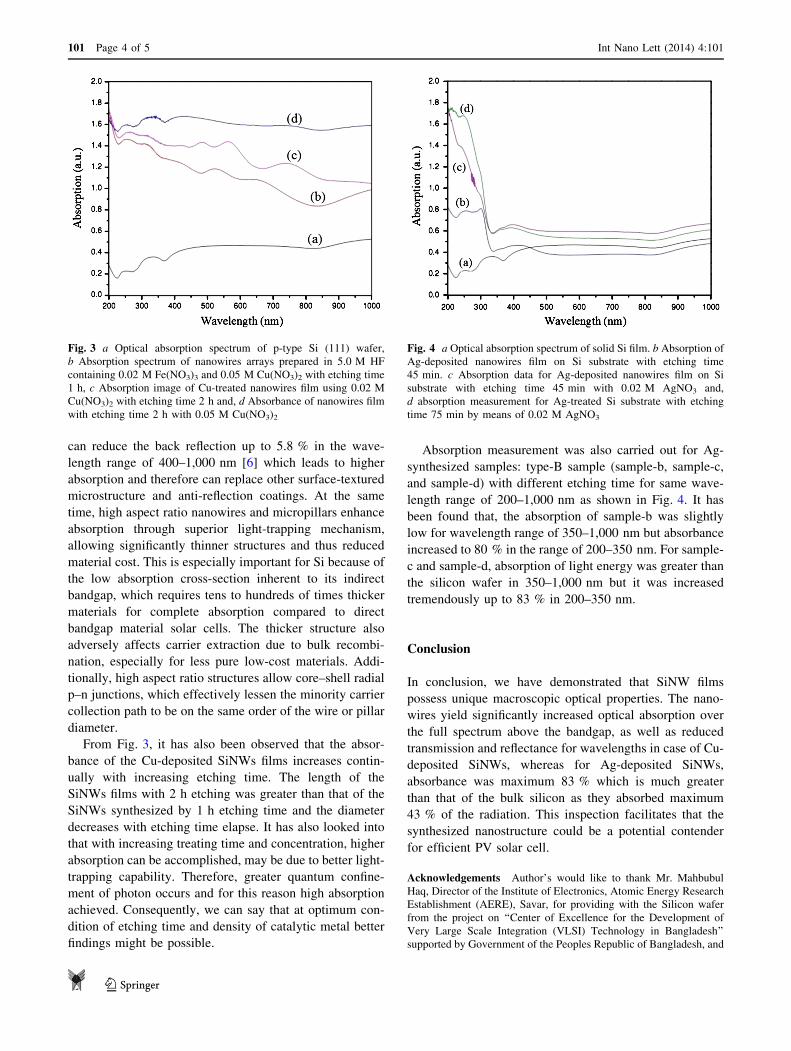
Figure 1 shows a schematic picture of top view of SEM
image and Fig. 2 shows a schematic picture of side view of
SEM image of SiNWs array fabricated on p-type Si sub-
strate. From the SEM micrograph, it has been seen that
SiNWs have formed with excellent vertical alignment,
uniformity, and packing density, with about 50 % area
density. The typical wire diameter from the SEM ranges
from 45 to 300 nm having length from 2 to 4 lm long.
Optical absorption spectra were obtained on a UV-1700
spectrophotometer employing halogen lamps, and equip-
ped to measure wavelength range from 200 to 1,000 nm.
The effective absorption (A) in the films was defined as
A = 1 - (T ? R) without any correction for thin film
effects or other possible losses, since comparisons of
samples on the same types of transparent substrate were
made.
Results and discussion
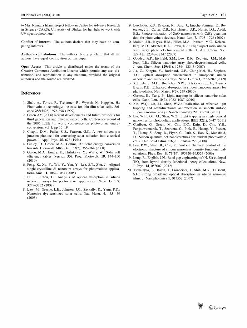
The absorption measurement was carried out over a range
of wavelengths 200 to 1,000 nm, which covers most of the
spectrum that is useful for SiNWs-based solar cells. Fig-
ure 3 shows typical total optical absorption spectra of Cu-
treated samples: type-A sample (sample-b, sample-c and
sample-d) along with absorption of bulk silicon (sample-a).
The absorbance of the solid silicon film shows typical
behavior as expected for silicon shown by Run et al. [19].
Here, we have noted that Si film’s absorption begin to
increase at 400 nm and remain almost steady up to
1,000 nm and might be decreased somewhere around
1,100 nm because of back-reflected loss for long wave-
length from top surface [20]. Si absorbs maximum of 47 %
of incident radiation, whereas absorption of SiNWs for Cu-
treated samples (sample-b, sample-c and sample-d of
Fig. 3) was maximum of 78 %. For sample-b, etching time
was 1 h and concentration of Cu(NO3)2 was 0.05 M.
Whereas for sample-c and sample-d, treating time was 2 h
with 0.02 and 0.05 M Cu(NO3)2.
From the above, we have observed that, absorption of
bulk Si film is much smaller than that of SiNWs array over
the same wavelength range. This is because by precisely
controlling the orientation (vertical vs. slanted), size (nano
vs. micro-scale), density and length of SiNWs reflectivity
can be reduced. It is also well known that, porous SiNWs
101 Page 2 of 5 Int Nano Lett (2014) 4:101
123
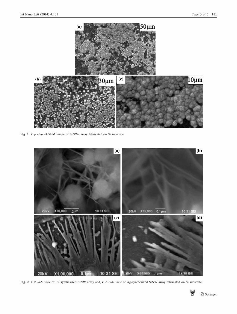
Fig. 1 Top view of SEM image of SiNWs array fabricated on Si substrate
Fig. 2 a, b Side view of Cu synthesized SiNW array and, c, d Side view of Ag-synthesized SiNW array fabricated on Si substrate
Int Nano Lett (2014) 4:101 Page 3 of 5 101
123
can reduce the back reflection up to 5.8 % in the wave-
length range of 400–1,000 nm [6] which leads to higher
absorption and therefore can replace other surface-textured
microstructure and anti-reflection coatings. At the same
time, high aspect ratio nanowires and micropillars enhance
absorption through superior light-trapping mechanism,
allowing significantly thinner structures and thus reduced
material cost. This is especially important for Si because of
the low absorption cross-section inherent to its indirect
bandgap, which requires tens to hundreds of times thicker
materials for complete absorption compared to direct
bandgap material solar cells. The thicker structure also
adversely affects carrier extraction due to bulk recombi-
nation, especially for less pure low-cost materials. Addi-
tionally, high aspect ratio structures allow core–shell radial
p–n junctions, which effectively lessen the minority carrier
collection path to be on the same order of the wire or pillar
diameter.
From Fig. 3, it has also been observed that the absor-
bance of the Cu-deposited SiNWs films increases contin-
ually with increasing etching time. The length of the
SiNWs films with 2 h etching was greater than that of the
SiNWs synthesized by 1 h etching time and the diameter
decreases with etching time elapse. It has also looked into
that with increasing treating time and concentration, higher
absorption can be accomplished, may be due to better light-
trapping capability. Therefore, greater quantum confine-
ment of photon occurs and for this reason high absorption
achieved. Consequently, we can say that at optimum con-
dition of etching time and density of catalytic metal better
findings might be possible.
Absorption measurement was also carried out for Ag-
synthesized samples: type-B sample (sample-b, sample-c,
and sample-d) with different etching time for same wave-
length range of 200–1,000 nm as shown in Fig. 4. It has
been found that, the absorption of sample-b was slightly
low for wavelength range of 350–1,000 nm but absorbance
increased to 80 % in the range of 200–350 nm. For sample-
c and sample-d, absorption of light energy was greater than
the silicon wafer in 350–1,000 nm but it was increased
tremendously up to 83 % in 200–350 nm.
Conclusion
In conclusion, we have demonstrated that SiNW films
possess unique macroscopic optical properties. The nano-
wires yield significantly increased optical absorption over
the full spectrum above the bandgap, as well as reduced
transmission and reflectance for wavelengths in case of Cu-
deposited SiNWs, whereas for Ag-deposited SiNWs,
absorbance was maximum 83 % which is much greater
than that of the bulk silicon as they absorbed maximum
43 % of the radiation. This inspection facilitates that the
synthesized nanostructure could be a potential contender
for efficient PV solar cell.
Acknowledgements Author’s would like to thank Mr. Mahbubul
Haq, Director of the Institute of Electronics, Atomic Energy Research
Establishment (AERE), Savar, for providing with the Silicon wafer
from the project on ‘‘Center of Excellence for the Development of
Very Large Scale Integration (VLSI) Technology in Bangladesh’’
supported by Government of the Peoples Republic of Bangladesh, and
Fig. 3 a Optical absorption spectrum of p-type Si (111) wafer,
b Absorption spectrum of nanowires arrays prepared in 5.0 M HF
containing 0.02 M Fe(NO3)3 and 0.05 M Cu(NO3)2 with etching time
1 h, c Absorption image of Cu-treated nanowires film using 0.02 M
Cu(NO3)2 with etching time 2 h and, d Absorbance of nanowires film
with etching time 2 h with 0.05 M Cu(NO3)2
Fig. 4 a Optical absorption spectrum of solid Si film. b Absorption of
Ag-deposited nanowires film on Si substrate with etching time
45 min. c Absorption data for Ag-deposited nanowires film on Si
substrate with etching time 45 min with 0.02 M AgNO3 and,
d absorption measurement for Ag-treated Si substrate with etching
time 75 min by means of 0.02 M AgNO3
101 Page 4 of 5 Int Nano Lett (2014) 4:101
123
to Mrs. Rumana Islam, project fellow in Centre for Advance Research
in Science (CARS), University of Dhaka, for her help to work with
UV spectrophotometer.
Conflict of interest The authors declare that they have no com-
peting interests.
Author’s contributions The authors clearly proclaim that all the
authors have equal contribution on this paper
Open Access This article is distributed under the terms of the
Creative Commons Attribution License which permits any use, dis-
tribution, and reproduction in any medium, provided the original
author(s) and the source are credited.
References
1. Shah, A., Torres, P., Tscharner, R., Wyrsch, N., Keppner, H.:
Photovoltaic technology: the case for thin-film solar cells. Sci-
ence 285(5428), 692–698 (1999)
2. Green AM (2006) Recent developments and future prospects for
third generation and other advanced cells. Conference record of
the 2006 IEEE 4th world conference on photovoltaic energy
conversion, vol 1. pp 15–19
3. Chapin, D.M., Fuller, C.S., Pearson, G.S.: A new silicon p-n
junction photocell for converting solar radiation into electrical
power. J. Appl. Phys. 25, 676 (1954)
4. Ginley, D., Green, M.A., Collins, R.: Solar energy conversion
towards 1 terawatt. MRS Bull. 33(2), 355–364 (2008)
5. Green, M.A., Emery, K., Hishikawa, Y., Warta, W.: Solar cell
efficiency tables (version 35). Prog. Photovolt. 18, 144–150
(2010)
6. Peng, K., Xu, Y., Wu, Y., Yan, Y., Lee, S.T., Zhu, J.: Aligned
single-crystalline Si nanowire arrays for photovoltaic applica-
tions. Small 1, 1062–1067 (2005)
7. Hu, L., Chen, G.: Analysis of optical absorption in silicon
nanowire arrays for photovoltaic applications. Nano. Lett. 7,
3249–3252 (2007)
8. Law, M., Greene, L.E., Johnson, J.C., Saykally, R., Yang, P.D.:
Nanowire dye-sensitized solar cells. Nat. Mater. 4, 455–459
(2005)
9. Leschkies, K.S., Divakar, R., Basu, J., Enache-Pommer, E., Bo-
ercker, J.E., Carter, C.B., Kortshagen, U.R., Norris, D.J., Aydil,
E.S.: Photosensitization of ZnO nanowires with CdSe quantum
dots for photovoltaic devices. Nano. Lett. 7, 1793–1798 (2007)
10. Maiolo, J.R., Kayes, B.M., Filler, M.A., Putnam, M.C., Kelzen-
berg, M.D., Atwater, H.A., Lewis, N.S.: High aspect ratio silicon
wire array photo electrochemical cells. J. Am. Chem. Soc.
129(41), 12346–12347 (2007)
11. Goodey, A.P., Eichfeld, S.M., Lew, K.K., Redwing, J.M., Mal-
louk, T.E.: Silicon nanowire array photoelectrochemical cells.
J. Am. Chem. Soc. 129(41), 12344–12345 (2007)
12. Jia, Z., Zongfu, Y., Burkhard, G.F., Ching-Mei, H., Stephen,
T.C.: Optical absorption enhancement in amorphous silicon
nanowire and nanocone arrays. Nano. Lett. 9(1), 279–282 (2009)
13. Kelzenberg, M.D., Boettcher, S.W., Petykiewicz, J.A., Turner-
Evans, D.B.: Enhanced absorption in silicon nanocone arrays for
photovoltaics. Nat. Mater. 9(3), 239 (2010)
14. Garnett, E., Yang, P.: Light trapping in silicon nanowire solar
cells. Nano. Lett. 10(3), 1082–1087 (2010)
15. Xie, W.Q., Oh, J.I., Shen, W.Z.: Realization of effective light
trapping and omnidirectional antireflection in smooth surface
silicon nanowire arrays. Nanotechnology 22, 065704 (2011)
16. Liu, W.F., Oh, J.I., Shen, W.Z.: Light trapping in single coaxial
nanowires for photovoltaic applications. IEEE 32(1), 5–47 (2011)
17. Conibeer, G., Green, M., Cho, E.C., Knig, D., Cho, Y.H.,
Fangsuwannarak, T., Scardera, G., Pink, E., Huang, Y., Puzzer,
T., Huang, S., Song, D., Flynn, C., Park, S., Hao, X., Mansfield,
D.: Silicon quantum dot nanostructures for tandem photovoltaic
cells. Thin Solid Films 516(20), 6748–6756 (2008)
18. Leu, P.W., Shan, B., Cho, K.: Surface chemical control of the
electronic structure of silicon nanowires: density functional cal-
culations. Phys. Rev. B. 73(19), 195320–195324 (2006)
19. Long, R., English, J.N.: Band gap engineering of (N, Si)-codoped
TiO2 from hybrid density functional theory calculations. New.
J. Phys. 14, 053007 (2012)
20. Tsakalakos, L., Balch, J., Fronheiser, J., Shih, M.Y., LeBoeuf,
S.F.: Strong broadband optical absorption in silicon nanowire
films. J. Nanophotonics 1, 013552 (2007)
Int Nano Lett (2014) 4:101 Page 5 of 5 101
123